JP4575647B2 - Method and apparatus for batch processing wafers in a furnace - Google Patents
Method and apparatus for batch processing wafers in a furnaceDownload PDFInfo
- Publication number
- JP4575647B2 JP4575647B2JP2003072732AJP2003072732AJP4575647B2JP 4575647 B2JP4575647 B2JP 4575647B2JP 2003072732 AJP2003072732 AJP 2003072732AJP 2003072732 AJP2003072732 AJP 2003072732AJP 4575647 B2JP4575647 B2JP 4575647B2
- Authority
- JP
- Japan
- Prior art keywords
- wafer
- support mechanism
- substrate support
- substrate
- cassette
- Prior art date
- Legal status (The legal status is an assumption and is not a legal conclusion. Google has not performed a legal analysis and makes no representation as to the accuracy of the status listed.)
- Expired - Lifetime
Links
Images


Classifications
- H—ELECTRICITY
- H01—ELECTRIC ELEMENTS
- H01L—SEMICONDUCTOR DEVICES NOT COVERED BY CLASS H10
- H01L21/00—Processes or apparatus adapted for the manufacture or treatment of semiconductor or solid state devices or of parts thereof
- H01L21/67—Apparatus specially adapted for handling semiconductor or electric solid state devices during manufacture or treatment thereof; Apparatus specially adapted for handling wafers during manufacture or treatment of semiconductor or electric solid state devices or components ; Apparatus not specifically provided for elsewhere
- H01L21/677—Apparatus specially adapted for handling semiconductor or electric solid state devices during manufacture or treatment thereof; Apparatus specially adapted for handling wafers during manufacture or treatment of semiconductor or electric solid state devices or components ; Apparatus not specifically provided for elsewhere for conveying, e.g. between different workstations
- H01L21/67763—Apparatus specially adapted for handling semiconductor or electric solid state devices during manufacture or treatment thereof; Apparatus specially adapted for handling wafers during manufacture or treatment of semiconductor or electric solid state devices or components ; Apparatus not specifically provided for elsewhere for conveying, e.g. between different workstations the wafers being stored in a carrier, involving loading and unloading
- H01L21/67778—Apparatus specially adapted for handling semiconductor or electric solid state devices during manufacture or treatment thereof; Apparatus specially adapted for handling wafers during manufacture or treatment of semiconductor or electric solid state devices or components ; Apparatus not specifically provided for elsewhere for conveying, e.g. between different workstations the wafers being stored in a carrier, involving loading and unloading involving loading and unloading of wafers
- H—ELECTRICITY
- H01—ELECTRIC ELEMENTS
- H01L—SEMICONDUCTOR DEVICES NOT COVERED BY CLASS H10
- H01L21/00—Processes or apparatus adapted for the manufacture or treatment of semiconductor or solid state devices or of parts thereof
- H—ELECTRICITY
- H01—ELECTRIC ELEMENTS
- H01L—SEMICONDUCTOR DEVICES NOT COVERED BY CLASS H10
- H01L21/00—Processes or apparatus adapted for the manufacture or treatment of semiconductor or solid state devices or of parts thereof
- H01L21/67—Apparatus specially adapted for handling semiconductor or electric solid state devices during manufacture or treatment thereof; Apparatus specially adapted for handling wafers during manufacture or treatment of semiconductor or electric solid state devices or components ; Apparatus not specifically provided for elsewhere
- H01L21/67005—Apparatus not specifically provided for elsewhere
- H01L21/67011—Apparatus for manufacture or treatment
- H01L21/67098—Apparatus for thermal treatment
- H—ELECTRICITY
- H01—ELECTRIC ELEMENTS
- H01L—SEMICONDUCTOR DEVICES NOT COVERED BY CLASS H10
- H01L21/00—Processes or apparatus adapted for the manufacture or treatment of semiconductor or solid state devices or of parts thereof
- H01L21/67—Apparatus specially adapted for handling semiconductor or electric solid state devices during manufacture or treatment thereof; Apparatus specially adapted for handling wafers during manufacture or treatment of semiconductor or electric solid state devices or components ; Apparatus not specifically provided for elsewhere
- H01L21/673—Apparatus specially adapted for handling semiconductor or electric solid state devices during manufacture or treatment thereof; Apparatus specially adapted for handling wafers during manufacture or treatment of semiconductor or electric solid state devices or components ; Apparatus not specifically provided for elsewhere using specially adapted carriers or holders; Fixing the workpieces on such carriers or holders
- H01L21/67346—Apparatus specially adapted for handling semiconductor or electric solid state devices during manufacture or treatment thereof; Apparatus specially adapted for handling wafers during manufacture or treatment of semiconductor or electric solid state devices or components ; Apparatus not specifically provided for elsewhere using specially adapted carriers or holders; Fixing the workpieces on such carriers or holders characterized by being specially adapted for supporting a single substrate or by comprising a stack of such individual supports
- H—ELECTRICITY
- H01—ELECTRIC ELEMENTS
- H01L—SEMICONDUCTOR DEVICES NOT COVERED BY CLASS H10
- H01L21/00—Processes or apparatus adapted for the manufacture or treatment of semiconductor or solid state devices or of parts thereof
- H01L21/67—Apparatus specially adapted for handling semiconductor or electric solid state devices during manufacture or treatment thereof; Apparatus specially adapted for handling wafers during manufacture or treatment of semiconductor or electric solid state devices or components ; Apparatus not specifically provided for elsewhere
- H01L21/673—Apparatus specially adapted for handling semiconductor or electric solid state devices during manufacture or treatment thereof; Apparatus specially adapted for handling wafers during manufacture or treatment of semiconductor or electric solid state devices or components ; Apparatus not specifically provided for elsewhere using specially adapted carriers or holders; Fixing the workpieces on such carriers or holders
- H01L21/6735—Closed carriers
- H01L21/67379—Closed carriers characterised by coupling elements, kinematic members, handles or elements to be externally gripped
- H—ELECTRICITY
- H01—ELECTRIC ELEMENTS
- H01L—SEMICONDUCTOR DEVICES NOT COVERED BY CLASS H10
- H01L21/00—Processes or apparatus adapted for the manufacture or treatment of semiconductor or solid state devices or of parts thereof
- H01L21/67—Apparatus specially adapted for handling semiconductor or electric solid state devices during manufacture or treatment thereof; Apparatus specially adapted for handling wafers during manufacture or treatment of semiconductor or electric solid state devices or components ; Apparatus not specifically provided for elsewhere
- H01L21/673—Apparatus specially adapted for handling semiconductor or electric solid state devices during manufacture or treatment thereof; Apparatus specially adapted for handling wafers during manufacture or treatment of semiconductor or electric solid state devices or components ; Apparatus not specifically provided for elsewhere using specially adapted carriers or holders; Fixing the workpieces on such carriers or holders
- H01L21/6735—Closed carriers
- H01L21/67383—Closed carriers characterised by substrate supports
- H—ELECTRICITY
- H01—ELECTRIC ELEMENTS
- H01L—SEMICONDUCTOR DEVICES NOT COVERED BY CLASS H10
- H01L21/00—Processes or apparatus adapted for the manufacture or treatment of semiconductor or solid state devices or of parts thereof
- H01L21/67—Apparatus specially adapted for handling semiconductor or electric solid state devices during manufacture or treatment thereof; Apparatus specially adapted for handling wafers during manufacture or treatment of semiconductor or electric solid state devices or components ; Apparatus not specifically provided for elsewhere
- H01L21/677—Apparatus specially adapted for handling semiconductor or electric solid state devices during manufacture or treatment thereof; Apparatus specially adapted for handling wafers during manufacture or treatment of semiconductor or electric solid state devices or components ; Apparatus not specifically provided for elsewhere for conveying, e.g. between different workstations
- H01L21/67763—Apparatus specially adapted for handling semiconductor or electric solid state devices during manufacture or treatment thereof; Apparatus specially adapted for handling wafers during manufacture or treatment of semiconductor or electric solid state devices or components ; Apparatus not specifically provided for elsewhere for conveying, e.g. between different workstations the wafers being stored in a carrier, involving loading and unloading
- H01L21/67769—Storage means
- H—ELECTRICITY
- H01—ELECTRIC ELEMENTS
- H01L—SEMICONDUCTOR DEVICES NOT COVERED BY CLASS H10
- H01L21/00—Processes or apparatus adapted for the manufacture or treatment of semiconductor or solid state devices or of parts thereof
- H01L21/67—Apparatus specially adapted for handling semiconductor or electric solid state devices during manufacture or treatment thereof; Apparatus specially adapted for handling wafers during manufacture or treatment of semiconductor or electric solid state devices or components ; Apparatus not specifically provided for elsewhere
- H01L21/683—Apparatus specially adapted for handling semiconductor or electric solid state devices during manufacture or treatment thereof; Apparatus specially adapted for handling wafers during manufacture or treatment of semiconductor or electric solid state devices or components ; Apparatus not specifically provided for elsewhere for supporting or gripping
- H01L21/6838—Apparatus specially adapted for handling semiconductor or electric solid state devices during manufacture or treatment thereof; Apparatus specially adapted for handling wafers during manufacture or treatment of semiconductor or electric solid state devices or components ; Apparatus not specifically provided for elsewhere for supporting or gripping with gripping and holding devices using a vacuum; Bernoulli devices
- H—ELECTRICITY
- H01—ELECTRIC ELEMENTS
- H01L—SEMICONDUCTOR DEVICES NOT COVERED BY CLASS H10
- H01L21/00—Processes or apparatus adapted for the manufacture or treatment of semiconductor or solid state devices or of parts thereof
- H01L21/67—Apparatus specially adapted for handling semiconductor or electric solid state devices during manufacture or treatment thereof; Apparatus specially adapted for handling wafers during manufacture or treatment of semiconductor or electric solid state devices or components ; Apparatus not specifically provided for elsewhere
- H01L21/683—Apparatus specially adapted for handling semiconductor or electric solid state devices during manufacture or treatment thereof; Apparatus specially adapted for handling wafers during manufacture or treatment of semiconductor or electric solid state devices or components ; Apparatus not specifically provided for elsewhere for supporting or gripping
- H01L21/687—Apparatus specially adapted for handling semiconductor or electric solid state devices during manufacture or treatment thereof; Apparatus specially adapted for handling wafers during manufacture or treatment of semiconductor or electric solid state devices or components ; Apparatus not specifically provided for elsewhere for supporting or gripping using mechanical means, e.g. chucks, clamps or pinches
- H01L21/68707—Apparatus specially adapted for handling semiconductor or electric solid state devices during manufacture or treatment thereof; Apparatus specially adapted for handling wafers during manufacture or treatment of semiconductor or electric solid state devices or components ; Apparatus not specifically provided for elsewhere for supporting or gripping using mechanical means, e.g. chucks, clamps or pinches the wafers being placed on a robot blade, or gripped by a gripper for conveyance
- Y—GENERAL TAGGING OF NEW TECHNOLOGICAL DEVELOPMENTS; GENERAL TAGGING OF CROSS-SECTIONAL TECHNOLOGIES SPANNING OVER SEVERAL SECTIONS OF THE IPC; TECHNICAL SUBJECTS COVERED BY FORMER USPC CROSS-REFERENCE ART COLLECTIONS [XRACs] AND DIGESTS
- Y10—TECHNICAL SUBJECTS COVERED BY FORMER USPC
- Y10S—TECHNICAL SUBJECTS COVERED BY FORMER USPC CROSS-REFERENCE ART COLLECTIONS [XRACs] AND DIGESTS
- Y10S414/00—Material or article handling
- Y10S414/135—Associated with semiconductor wafer handling
- Y10S414/136—Associated with semiconductor wafer handling including wafer orienting means
Landscapes
- Engineering & Computer Science (AREA)
- Physics & Mathematics (AREA)
- Condensed Matter Physics & Semiconductors (AREA)
- General Physics & Mathematics (AREA)
- Manufacturing & Machinery (AREA)
- Computer Hardware Design (AREA)
- Microelectronics & Electronic Packaging (AREA)
- Power Engineering (AREA)
- Robotics (AREA)
- Container, Conveyance, Adherence, Positioning, Of Wafer (AREA)
Description
Translated fromJapanese【0001】
【発明の属する技術分野】
本発明は、一般に半導体製造に関し、より詳細には、炉内でのバッチ処理のためにウェハを移送して支持するための方法および装置に関する。
【0002】
【従来の技術】
熱に関連する複雑さが、炉内でウェハのバッチを非常に高い温度で扱う、または処理する、例えば最大約1350℃の温度で処理するために一般的なウェハボートを使用することを妨げる可能性がある。例えば、一般的なウェハボートでは、縁部でのみウェハを支持することができる。そのような支持スキームでは、非常に高い温度ではウェハの機械的強度が低減することがあるため、ウェハ自体の重量によって、非常に高い温度でウェハを塑性変形する可能性がある。
【0003】
他の利用可能なウェハボートウェハ支持機構が特許文献1および特許文献2に記載されている。特許文献1は、複数の内側位置でウェハを支持するために複数の内側延在アームを有するウェハ支持機構を有するウェハボートに関するものである。特許文献2は、リング支持機構の円周全体を使用して、中心位置でウェハを支持するウェハボートに関するものである。しかし、これらのウェハボードでの支持機構は、依然として、ウェハの塑性変形および結果として生じる結晶学的すべりを防止するのに十分な支持性を有しない。すべりを防止するために、ウェハを、底面領域の実質的な部分にわたって支持する必要がある。
【0004】
この基準に見合うウェハ支持機構が、単一ウェハシステムに関して知られている。そのようなシステムでは、底面領域全体にわたってウェハを支持するサセプタと、周縁でウェハを支持するために完全な円を形成する支持リングとが従来技術において知られている。しかし、そのようなサセプタ上にウェハを配置するために、またはサセプタからウェハを分離するために特別の措置が必要である。
【0005】
特に、そのような単一ウェハシステムでは、従来技術によるロボットエンドエフェクタを使用するとき、ウェハへのアクセスは通常、底部からなされ、サセプタはプロセスチャンバ内部で定位に留まり、ウェハは直列に装填され、装填解除される。一般的には、ロボットエンドエフェクタは、サセプタの上のレベルで可動ピン上にウェハを配置し、ウェハはサセプタの十分上方に間隔を空けて配置されて、ウェハまたはサセプタにロボットエンドエフェクタが接触することなくロボットエンドエフェクタを引き抜くための十分なクリアランスを可能にする。引抜き後、ピンは下方向に移動して、ウェハをサセプタまで下げる。ウェハを装填解除するためには、これらのステップの逆が行われる。そのようなウェハ装填および支持システムは、単一ウェハ処理に適している一方で、バッチ処理システムに簡単には適用可能でない。これは、可能であったとしても、とりわけ、あらゆる処理位置が可動ピンと、これらのピンを移動するための関連ハードウェアおよび制御システムとを備える必要があるので、そのようなシステムは受け入れられないほど複雑で、扱いにくくなるためである。
【0006】
【特許文献1】
米国特許第5865321号明細書
【特許文献2】
米国特許第5820367号明細書
【0007】
【特許文献3】
米国特許第4407654号明細書
【特許文献4】
米国特許第4770590号明細書
【特許文献5】
米国特許第5162047号明細書
【特許文献6】
米国特許第5192371号明細書
【特許文献7】
米国特許第5219079号明細書
【特許文献8】
米国特許第5310339号明細書
【特許文献9】
米国特許第5316472号明細書
【特許文献10】
米国特許第5334257号明細書
【特許文献11】
米国特許第5407449号明細書
【特許文献12】
米国特許第5482558号明細書
【特許文献13】
米国特許第5482559号明細書
【特許文献14】
米国特許第5492229号明細書
【特許文献15】
米国特許第5556147号明細書
【特許文献16】
米国特許第5556275号明細書
【特許文献17】
米国特許第5858103号明細書
【特許文献18】
米国特許第5897311号明細書
【特許文献19】
米国特許第5931666号明細書
【特許文献20】
米国特許第6099302号明細書
【特許文献21】
米国特許第6203617号明細書
【特許文献22】
米国特許第6287112号明細書
【特許文献23】
米国特許第6321680号明細書
【特許文献24】
米国特許第6341935号明細書
【特許文献25】
米国特許第6361313号明細書
【特許文献26】
米国特許第6390753号明細書
【特許文献27】
米国特許第6464445号明細書
【特許文献28】
欧州特許出願公開第86308980.1号明細書
【特許文献29】
国際公開第00/68977号パンフレット
【特許文献30】
特開昭63−10225号公報
【0008】
【発明が解決しようとする課題】
したがって、本発明の目的は、とりわけ、底面領域の実質的な部分にわたるウェハに関する支持機構を提供し、プロセスチャンバで処理するためのウェハの効率の良い装填および装填解除を可能にするウェハ支持システムをウェハボートに提供することである。
【0009】
【課題を解決するための手段】
本発明の1つの好ましい実施形態によれば、半導体処理のための方法が提供される。この方法は、ウェハ支持機構上にウェハを配置するステップと、その後、ウェハ支持機構上に配置された状態で、ウェハをウェハボート内に輸送するステップと、ウェハボート内で、ウェハがウェハ支持機構上に配置された状態でウェハに半導体製造プロセスを施すステップとを含む。
【0010】
他の好ましい実施形態によれば、処理のためにウェハおよびウェハ支持機構を取り扱うための方法が提供される。この方法は、移送ステーション内でウェハ支持機構上にウェハを装填するステップと、ウェハを、移送ステーションからプロセスチャンバ内に輸送するステップと、プロセスチャンバ内でウェハに半導体製造プロセスを施すステップとを含む。ウェハをプロセスチャンバ内に輸送し、ウェハに半導体製造プロセスを施す間、ウェハはウェハ支持機構上に配置されている。
【0011】
さらに別の好ましい実施形態によれば、基板を処理するためのシステムが提供される。システムは、複数の基板を支持するための複数の基板支持機構を含む。
基板支持機構は、基板の周縁全体を支持し、基板支持ホルダ内に保持され、基板支持ホルダから取り外すこともできる。プロセスチャンバは、基板処理中に基板支持ホルダを収容する。システムはまた、基板支持機構上に基板を装填するように構成された、基板支持ホルダとは異なる基板装填ステーションを備える。
【0012】
別の好ましい実施形態によれば、半導体ウェハカセットが提供される。カセットは、ウェハ支持機構上にウェハを装填するように構成されたウェハ装填ステーションを収容する。
【0013】
本発明は、本発明を例示するためのものであり、制限するためのものではない好ましい実施形態の詳細な説明、および添付図面からより良く理解されよう。
【0014】
【発明の実施の形態】
本発明の好ましい実施形態について以下に図面を参照して説明する。
【0015】
本発明の好ましい実施形態によれば、半導体製造プロセス中にウェハを支持するためのウェハ支持機構が提供される。ウェハ支持機構は、ウェハ支持ホルダの格納収容部に取外し可能に格納することができる。ウェハ支持ホルダは、半導体処理に使用される標準的なウェハボートと同様であり、炉内での処理中にウェハおよびウェハ支持機構を保持する。ウェハ支持機構はまた、ウェハとはわずかに異なる寸法のウェハ支持機構を収容するように適合されている前開き一体形ポッド(FOUP)などウェハ処理カセットの格納収容部内に取外し可能に格納することができる。ウェハ支持機構は、ウェハの周縁全体にわたってウェハを支持することが好ましく、この場合、望ましいことに、ウェハ支持機構は、ウェハの周縁全体の周りに延在しない支持機構に比べてフープ強度が高くなる。ウェハ支持機構がウェハの実質的な部分を支持することがより好ましい。一実施形態では、支持機構が、ウェハの底面全体を支持することができる材料のプレートを備えることができる。他の実施形態では、ウェハ支持機構はリング形状にすることができる。ウェハの「実質的な部分」を支持する際、ウェハ支持機構は、ウェハの底面の約10%よりも多く、好ましくは約50%よりも多く、より好ましくは約90%よりも多くをカバーするようにウェハの下に延在する。
【0016】
本発明の好ましい実施形態によるウェハ支持機構に加えて、ウェハ支持機構上にウェハを配置するため、およびウェハ支持機構からウェハを取り外すために、移送または装填ステーションも提供される。移送ステーションは、第1のレベルにあるウェハ支持機構用の収容部と、第1のレベルよりも上の第2のレベルにあるウェハ用の収容部とを備える。装填中、はじめはそれぞれ第2および第1のレベルにあるウェハおよびウェハ支持機構が接触される。接触時、ウェハはウェハ支持機構上に配置される。装填解除中、はじめは同じレベルにあるウェハとウェハ支持機構が分離され、それぞれ第2および第1のレベルに位置するようになる。
【0017】
本発明の好ましい実施形態によるウェハのバッチを装填して処理するための例示処置の流れ図が、図1に概略的に与えられている。参照番号10によって示されるように、ウェハ支持機構は、ウェハ支持機構格納位置から移送ステーションに輸送される。この移送は、ウェハ輸送のために設計されたロボットエンドエフェクタを使用して行うことができる。ロボットエンドエフェクタは、底部からウェハ支持機構に接触し、ウェハ支持機構を移送ステーションに輸送する。移送ステーションで、ロボットは、ウェハ支持機構を第1のレベルに配置する。
【0018】
参照番号12によって示されるように、ウェハも移送ステーションに輸送される。ウェハは、第1のレベルよりも上にある移送ステーション内の第2のレベルを占める。
【0019】
次いで、参照番号14によって示されるように、依然として移送ステーション内にある状態で、ウェハがウェハ支持機構上に配置される。次いで、参照番号16によって示されるように、ウェハが、そのウェハが配置されているウェハ支持機構と共に、ウェハ支持ホルダまたは「ボート」に輸送される。
【0020】
参照番号18によって示されるステップで、システムが、ウェハのバッチの装填が完了したかどうかチェックする。システムが、示したステップをロボットおよび他のシステム機構を制御することによって行うようにプログラムされたプロセッサおよびメモリを含むことを理解されたい。装填が完了していない場合、ループ24によって示されるように、前の手順が繰り返される。ウェハは、順次に、例えば最上部スロットから最下部スロットに、ウェハ支持ホルダ内に装填されることが好ましい。装填が完了したとき、例えば、好ましくはウェハ支持機構上に支持された完全なウェハのバッチがウェハ支持ホルダ内に装填されたとき、参照番号20によって示されるように、ウェハ支持ホルダが、炉などプロセスチャンバ内に装填される。あるいは、ウェハ/支持機構組合せの装填を、ウェハ支持ホルダがプロセスチャンバ内部に配置された状態でドアを通して行うことができる。
【0021】
参照番号22によって示されるように、プロセスチャンバ内でウェハに処理が施される。有利には、処理は非常に高い温度で、好ましくは約1000℃よりも高い温度で、より好ましくは約1200℃よりも高い温度で、最も好ましくは約1300℃よりも高い温度で行うことができる。処理後、ウェハは逆順で装填解除される(図示せず)。
【0022】
移送ステーション内外へのウェハ支持機構とウェハの移送は、同じロボットおよび同じエンドエフェクタを使用して行われることが好ましい。しかし、ウェハ支持機構およびウェハを移動させるために、様々なロボットおよび/または様々なエンドエフェクタを他の構成で使用することもできることを理解されたい。特に、使用されるウェハ支持機構に応じて、ロボットエンドエフェクタを、縁部でウェハ支持機構とウェハの両方に接触する縁部支持エンドエフェクタにすることも、底面の中心に向けてウェハ支持機構とウェハの両方に接触するより従来型のエンドエフェクタにすることも、これら2つのエンドエフェクタの組合せ、例えば、縁部でウェハ支持機構に接触し、底面の中心に向けてウェハに接触するエンドエフェクタにすることもできる。より一般には、エンドエフェクタは、ウェハ支持機構およびウェハを保持し、本明細書で述べる作用を行うのに適した任意のエンドエフェクタにすることができる。例えば、縁部支持エンドエフェクタはリング形状ウェハ支持機構に特に適しており、一方、プレートであるウェハ支持機構は、ウェハ支持機構の縁部、またはウェハ支持機構の底面のより中心の領域でウェハ支持機構に接触するエンドエフェクタを用いて保持することができる。例示的なエンドエフェクタは、2002年5月2日に出願の米国仮特許出願60/377904号、およびそれに対応する、den Hartogによって2003年2月5日に出願された「TWO LEVEL END EFFECTOR」という名称の米国実用新案出願10/361480号に開示されており、それらの開示を参照により本明細書に組み込むものとする。
【0023】
ウェハを支持するウェハ支持機構は、円形プレート、すなわちその上に配置されるウェハの底面領域全体を支持する構造を備えることが好ましい(図5Aおよび6A、および以下のそれに対応する本文を参照のこと)。ウェハ支持機構は、リングの形状、すなわち中心が空いた構造にすることもできる(図5Bおよび6B、および以下のそれに対応する本文を参照のこと)。支持「リング」は円形状を有することができるが、円形である必要はなく、関連する装置がその形状を受け入れるように構成されている限り、例えば六角形、さらには正方形にすることもできる。
【0024】
一実施形態では、ウェハ支持機構は、処理システム内に永久的に留まることができる。例えば、処理前後にウェハ支持ホルダ内に格納することができる。別の実施形態では、ウェハ支持機構は、カセット内、より詳細には、ウェハ支持機構を収容するように適合されたFOUP内で、処理システム内に格納され、供給される。この適合は、FOUP内部でウェハ支持機構を保持するための支持フレームがFOUPの標準的な構成から変化することのみを必要とする。したがって、FOUPの外面は、その標準的な構成を保つことができる。ウェハ支持機構は、300mmウェハを支持するように構成され、したがって、300mmウェハの直径よりもわずかに大きな直径を有することが好ましい。
【0025】
さらに、1つの好ましい実施形態では、移送ステーションが、ウェハ支持機構を保持するFOUPの一部として提供される。これらの適合されたFOUPは、FOUPドアオープナを備える市販のFOUP受取りステーションを介して処理システムと連結することができる。したがって、この実施形態は、既存のシステムを後付けするように特に良く適合されている。さらに、移送ステーションを、FOUPの上端部と下端部の間の任意の点に、または上端部または下端部のどちらかに位置付けることができる。移送ステーションがFOUPの下端部に位置付けられることが好ましい。
【0026】
好ましくは、ウェハも、カセット内で処理システムに供給される。300mmの直径を有するウェハに関しては、標準的なFOUPが、ウェハを処理システムに提供するために使用されるカセットとして働くことが好ましい。FOUPは、処理システム内に提供されたFOUPドアオープナを備えるFOUPステーションと連結する。したがって、別の実施形態では、ウェハ支持機構を格納するFOUPが移送ステーションを含むことができるのと同様に、ウェハを格納するFOUPも移送ステーションを含むことができる。有利には、処理システム内にウェハ支持機構が永久的に留まる処理システム内で使用されるとき、そのようなFOUPは、例えば個別の移送ステーションを処理システムに有意に後付けする必要性を含まない。さらに別の実施形態では、FOUPがウェハを格納するか、ウェハ支持機構を格納するかに関係なく、移送ステーションが構造内に存在することもできる。
【0027】
移送ステーション内部で、移送ステーション内のウェハおよびウェハ支持機構収容部が、ウェハ支持機構上にウェハを装填し、装填解除するために使用される様々なタイプの支持構造を備えることができる。したがって、ウェハ支持機構上へのウェハの配置は、いくつかの方法で行うことができる。例えば、一実施形態では、ウェハは静止したままで、ウェハ支持機構用の支持構造を垂直方向で可動にすることができる。別の実施形態では、ウェハ用の支持構造を垂直方向で可動にすることができ、ウェハ支持機構は静止したままである。さらに別の実施形態では、ウェハ用の支持機構とウェハ支持機構用の支持構造との両方が可動である。例えば、ウェハ支持機構およびウェハを格納収容部内に配置した後、ウェハ用の支持構造は、ウェハがウェハ支持機構上に位置するまでウェハ支持機構に向けて移動されるように移動することができる(あるいはその逆であり、またはウェハとウェハ支持機構の両方が移動することができる)。ウェハ支持機構が、好ましくは切欠き(例えばスルーホール)を備えて、ウェハ支持機構自体とは関係なく、それら支持構造およびウェハの垂直移動を可能にする。
【0028】
特に単純な他の実施形態では、移送ステーション内の全ての支持構造が静止している。ウェハをウェハ支持機構上に配置するための垂直移動は、ウェハに接触するようにウェハ支持機構を上に向けて輸送するロボットによって行われる。したがって、好ましい実施形態は、有利には、ウェハの周縁全体を含めたウェハの底面領域の実質的な部分を支持するウェハ支持機構上で、ウェハをプロセスチャンバに提供することができる。
【0029】
次に図面を参照する。図面を通して、同じ参照番号が同じ部分を指す。
【0030】
図2および3を参照すると、プロセスチャンバを含む例示的なウェハ処理システムが図示され、一般に参照番号30によって示されている。図2および3の例示システム30は、ハウジング32を備え、一般にはいわゆる「クリーンルーム」内に設置されている。ハウジング32に加えて、隔壁33、34、および35(図を見やすくするために図2からは省かれている)も存在する。ハウジング32は、隔壁33と共に処理チャンバ51の範囲を定める。処理領域51は反応器を備え、反応器はこの場合、垂直炉36、37である。ハウジング32と隔壁33および34とが、ウェハ取扱いセクションまたはチャンバ52を画定する。カセット移送セクションまたはチャンバ53が、ハウジング32と隔壁34および35との間に画定される。システム30内外にカセットを移送するための入出力ステーションが参照番号63によって示されている。
【0031】
ウェハが、入出力ステーション63に配置されているカセット40内に供給される。好ましい実施形態によるFOUPが、好ましくはカセット40として働く。カセット取扱いデバイス61が、入出力ステーション63から閉鎖可能開口64を通して、カセット移送セクション53内に位置付けられたカセットストア38内にカセット40を移送する。カセットストア38は、カセット40が格納される、垂直方向に位置合わせされたいくつかのロータリプラットフォーム57を備える。カセット取扱いデバイス61は、様々なプラットフォーム57に到達することができるように、エレベータ65によって垂直方向に可動である。カセット取扱いデバイス61はカセットエンドエフェクタ62を備え、カセットエンドエフェクタ62は、ロータリプラットフォーム57の一連の切欠き56の寸法よりもわずかに小さい寸法を有する。カセット取扱いデバイス61がストア38内にカセット40を移送するとき、カセット取扱いデバイス61のエンドエフェクタ62を、プラットフォーム57の1つの切欠き56の1つを通して下げて、プラットフォーム57上にカセット40を配置することができる。その後、カセット取扱いデバイス61をカセットストア38から引き抜くことができる。カセット取扱いデバイス61は、入出力ステーション63とストア38の間でカセット40を移送することができるように取り付けられている。デバイス61は、ストア38と回転可能カセット移送プラットフォーム60との間で、または入出力ステーション63と回転可能カセット移送プラットフォーム60との間でカセット40を移送することもできる。
【0032】
回転可能カセット移送プラットフォーム60は、回転時に、カセット移送セクション53とウェハ取扱いセクション52の間の隔壁34に対してカセット40が配置されるように構成されている。隔壁34は、クロージャとクロージャ機構を備え、これらが、参照番号67によって概略的に示される境界面を形成する。
隔壁34での境界面67に対してカセットを配置した後、クロージャ機構が、カセットのクロージャを把持し、ロック解除し、隔壁34のクロージャとカセットのクロージャとを同時に開く。
【0033】
ウェハ取扱いセクション52内部のウェハ取扱いデバイス54が、当該のカセットとウェハ支持ホルダ42との間でウェハを移送する。ウェハ支持ホルダ42は、好ましい実施形態のカセット内に保持することができるウェハよりも多くのウェハ、すなわち、現在標準的なFOUPを使用するときには25枚よりも多くのウェハ、好ましくは50枚よりも多くのウェハ、より好ましくは70枚よりも多くのウェハを収容する。本明細書で述べるように、ウェハ取扱いデバイス54は、個々のウェハを取り扱うように構成されたロボットエンドエフェクタ59を備えることが好ましい。ウェハをウェハ支持ホルダ42内に装填するために、ウェハ取扱いデバイス54はまず、カセット40から、例えばカセット40内に含まれる移送ステーションにウェハを移送し、次いで、例えばウェハ支持ホルダ42内に含まれる格納位置から移送ステーションにウェハ支持機構を移送する。ウェハをウェハ支持機構上に配置した後、ウェハ支持機構上に設置されたウェハが、ウェハ支持ホルダ42内に装填される。ウェハ支持ホルダ42はそれぞれ、ペデスタル上に支持されたウェハボートまたはラックを備えることが好ましい。ドアプレートが、各ペデスタルの下に提供されることが好ましい。
【0034】
ウェハを含むFOUPまたはカセット40内部に移送ステーションが含まれていない場合、個別の移送ステーション(図示せず)がウェハ取扱いセクション52内に提供されることは明らかである。また、別の実施形態では、好ましくはウェハとウェハ支持機構との両方が、各FOUPごとに境界面67にクロージャ(図示せず)を有して、FOUP内で処理システム30に提供されていてもよい。
そのような実施形態では、2つの回転可能なカセットプラットフォーム60が両方のFOUP(図示せず)に向き、それにより前記FOUPがウェハ取扱いセクション52に対して同時に開かれる。
【0035】
ウェハ支持ホルダ42内へのウェハの装填が完了した後、移送アーム46が、好ましくは、ウェハ取扱いチャンバ52から処理チャンバ51内に隔壁33の開放可能クロージャ49を通して、ウェハ支持ホルダ42を支持表面47上に移動する。例示した処理セクション51は、複数のウェハ支持ホルダ42を支持するロータリ移送プラットフォーム41を備える。この場合は炉36、37を備える2つの反応器が処理チャンバ51内に配置されている。炉36、37は、垂直に配置され、ウェハ/ウェハ支持組合せ43を充填されたウェハ支持ホルダ42が下から炉36、37内に垂直に導入される。このために、各炉36、37は、垂直方向で可動な挿入アーム44を有する。ウェハ支持ホルダ42の下のドアプレートは、ウェハ支持ホルダ42が反応器内に持ち上げられたときに、外側処理セクションから反応器を封止する働きをする。
【0036】
多数のウェハの処理は以下のように行うことができる。図2に概略的に示される操作者が、入出力ステーション63にいくつかのカセット40を導入し、制御パネル66で制御操作を行うことによってストア38に装填する。各カセット40が、入出力ステーション63から、カセット取扱いデバイス61を使って、ストア38内にこれらのカセットのために作成された格納コンパートメント39内に、具体的にはスタックロータリプラットフォーム57上に移送される。ストア38の回転およびエレベータ65の使用により、様々なコンパートメントにカセット40を充填することができる。ストア38に充填した後は、この例示自動設置により、さらなる人の干渉は必要ない。
【0037】
次いで、当該のカセット40が、カセット取扱いデバイス61によってストア38から取り外されて、カセット移送プラットフォーム60上に配置される。カセット移送プラットフォーム60は、図2に概略的に示される2つのレベルを備え、各レベルがカセットを受け取ることができ、2つのレベルは、互いに関係なく回転することができる。カセット移送プラットフォーム60の回転後、カセットは隔壁34に対して配置される。有利には、移送ステーションがFOUP内に配置されてプロセスチャンバ51にウェハまたはウェハ支持機構を提供する実施形態では、1つのプラットフォーム60が、ウェハを提供するためのFOUPを収容することができ、他のプラットフォームが、ウェハ支持機構を提供するためのFOUPを収容する。次いで、両方のレベルでのFOUPを、取扱いチャンバ52に同時に開くことができる。任意の場合に、隔壁34のクロージャ67と共にカセットのクロージャを開いた後、ウェハがウェハハンドラ54によって取り外され、移送ステーションに輸送され、ウェハ支持機構上に配置され、ウェハ/支持機構組合せ43がウェハ支持ホルダ42内に配置される。ウェハ支持ホルダ42が充填され、反応器36、37の1つに関して利用可能になった後、隔壁33のクロージャ49が開かれ、ウェハボートまたは支持ホルダ42が、移送アーム46によって移送プラットフォーム41上に配置される。次いで、移送プラットフォーム41は、プロセスチャンバ51内部のウェハ支持ホルダ42を、装填する反応器の下の位置に移動する。次いで、挿入機構またはエレベータ44が、ウェハ支持ホルダ42を反応器36または37内に移動させる。処理されたウェハは、プロセスチャンバ51内部で下げられて冷却された後に、上述したコースを逆順に移動する。
【0038】
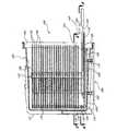
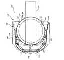
上述したように、ウェハ支持機構は、閉鎖可能FOUPなどカセット内で処理システムに提供することができる。ここで、図4を参照すると、本発明の好ましい実施形態によるFOUPが、参照番号100によってその全体を示されている。FOUP100は、ドア110(図5Aおよび5B)を受け取るために一端にフランジ104を備えるハウジング102を備える。FOUP100の底部に、支持テーブル上にFOUP100を支持するための機械的境界面106が提供されることが好ましい。ハウジング102および底部境界面106を含めたFOUP100の外面は、SEMIスタンダードに従って構成されていることが好ましい。
【0039】
ハウジング102内部に支持構造120が提供される。支持構造120は、ボルト122を用いてハウジングの下側に取り付けられる。
【0040】
ウェハ支持機構140を保持するために表面132および138を備える垂直方向延在支持ビーム130および136が支持構造120に取り付けられている。各表面132が、傾斜付き側面を有する支持リッジ134を備える。支持リッジ134は、ウェハ支持機構140の穴142内に嵌合して、ウェハ支持機構140に関する中心合わせおよび位置決め能力を提供する。ウェハ支持機構140を一体となって収容するための表面132および138、支持リッジ134、ならびにFOUP内部の体積が、格納収容部141を構成する。合計で、ウェハ支持機構140に関する23箇所の格納収容部141が例示されており、その最下部の収容部141は空の状態で示されている。
【0041】
例示したFOUP100とは適合していない形態においては、25枚のウェハ160を収容することができることを理解されたい。しかし、例示したように、25枚のウェハ160を収容するように設計されたカセット内に2箇所の追加の格納収容部141が元々見られるFOUP100の下端部には、代わりに移送ステーション143が提供されることが好ましい。移送ステーション143は、好ましくは3つのピン150を備え、各ピンは、ウェハ支持機構140を支持することができる円錐下端部152と、上にウェハ160を支持することができる円柱形上部153とを備える。好ましくは、ピン150の材料は、PEEK(商標)(ポリエーテルエーテルケトン)、またはTeflon(商標)やポリプロピレンなどウェハに損傷を加えない別の材料である。ピン150の円柱形上部153の通過を可能にするように、各ウェハ支持機構140が3つの穴142を備えることが好ましい。
【0042】
ウェハ支持機構140上にウェハ160を配置するために、ウェハ支持機構140が、FOUP100内の格納収容部141から移送ステーション143に移送される。格納収容部141は、支持機構140の意図していない接触を伴わずに、隣接するウェハ支持機構140間でロボットエンドエフェクタ154が移動することができる十分な高さを有する。ウェハ支持機構140を移送するために、ロボットエンドエフェクタ154は、ウェハ支持機構140にその底部から接触し、ウェハ支持機構140を表面132および138から、かつ支持リッジ134から離す。次いで、ウェハ支持機構140は、エンドエフェクタ154上にある状態で、その格納収容部141から、FOUP100の下端部に提供される移送ステーション143にロボットによって移動される。ロボットは、支持機構の穴142が支持ピンの円柱形上部153にわたって通り、ウェハ支持機構が支持ピン150の円錐部152上に位置するようにウェハ支持機構140を配置する。
【0043】
上述したように、ウェハ支持機構140の位置を、支持リッジ134によって格納収容部141内でロックすることができる。有利には、このロックは、移送ステーション143に輸送されるようにウェハ支持機構140が正確に向けられ、それによりウェハ支持機構140が移送ステーション143に移動されるときにウェハ支持機構140の穴142の位置がピン150の位置と位置合わせされることを保証する。
【0044】
ウェハ支持機構140が移送ステーション143に移送された後、ウェハ160も移送ステーション143に移送され、ピン150の上部に配置される。エンドエフェクタ154が、ウェハ160と接触しないように下がり、次いでウェハ160またはウェハ支持機構140の意図してない接触を伴わずに、ピン150上に支持されたウェハ160の下面とピン150の円錐部152上に支持されたウェハ支持機構140の上面との間で引き抜かれて移動されるのに十分な空間が存在するように、ピン150の上端部は十分に高いことを理解されたい。
【0045】
ウェハ160を下げて、ウェハ160をピン150の上部に配置した後、ロボットがエンドエフェクタ154を引き抜き、ウェハ支持機構140の下面よりも下のレベルに垂直にエンドエフェクタ154を移動させ、次いで再び延ばし、それにより、上述したように、ピン150の円錐部152に配置されているウェハ支持機構140の下にエンドエフェクタ154がこのとき配置される。次に、エンドエフェクタ154は上方向に移動する。その際、エンドエフェクタ154は、ウェハ支持機構140に接触して持ち上げて、ウェハ支持機構140をウェハ160に接触させて持ち上げる。そのように移動することによって、ウェハ支持機構140とウェハ160の両方が、ピン150の上に持ち上げられて、ウェハ160はウェハ支持機構140上に位置する。次いで、ロボットは、ウェハ160と共にウェハ支持機構140をボートまたはウェハ支持ホルダ42(図2)に輸送することができ、ここでウェハ160に半導体製造プロセスが施される。
【0046】
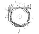
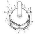
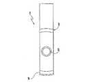
図5Aおよび5Bは、FOUP100の断面上面図を例示し、各図においてFOUP100のドア110が閉じた位置で示されている。図5Aでは、ウェハ支持機構140は円形プレートであり、図5Bでは、ウェハ支持機構140が、円形状および内周または境界146を有するリングである。図5Aおよび5Bそれぞれにおいて、ウェハ支持機構140が、ドア110と反対側で、支持リッジ134によって格納向きでロックされていることは注目に値する。さらに、ウェハ支持機構140は、好ましくは、処理中の余剰熱放射からウェハ160の縁部を遮蔽することができる隆起縁部144(図9)を有する。
【0047】
図6Aおよび6Bは、FOUP100内の移送ステーション143の断面上面図を例示し、図6Aでのウェハ支持機構140は円形プレートであり、図6Bでのウェハ支持機構140は円形リングである。図6Aに例示されるように、エンドエフェクタ154は、ウェハ支持機構140および/またはウェハ160(図示せず)にその底面で、典型的にはその中心で接触することができる。そのような例示エンドエフェクタは、2002年5月2日に出願の米国仮特許出願60/377904号、およびそれに対応する、den Hartogによって2003年2月5日に出願された「TWO LEVEL END EFFECTOR」という名称の米国実用新案出願10/361480号に記載されており、それらの開示を参照により本明細書に組み込む。図6Bで、エンドエフェクタ154は、リングの直径にわたって延在して、ウェハ支持機構140および/またはウェハ160(図示せず)の反対側に接触し、例えば縁部支持エンドエフェクタにすることができる(図6Bおよび7を参照のこと)。そのような例示縁部支持エンドエフェクタも、米国仮特許出願60/377904号、およびden Hartogによって2003年2月5日に出願された「TWO LEVEL ENDEFFECTOR」という名称の米国実用新案出願10/361480号に記述されている。縁部支持エンドエフェクタは、ウェハ支持機構140がプレートであれリングであれ、ウェハ支持機構140と共に使用するのに適していることを理解されたい。
【0048】
図6Aおよび6Bそれぞれにおいて、ウェハ支持機構140はピン150上に位置し、エンドエフェクタ154はウェハ支持機構140の下に存在する。FOUP100の機械側境界面が参照番号108で示されている。ウェハ支持機構140は、移送ステーション143でピン150上に位置した状態で、好ましくは、格納収容部141内に収容されたウェハ支持機構140に対して外方向に移動される。このようにすると、ウェハ支持機構140は、支持ビーム136から十分に離れ、それによりウェハ支持機構140を、ウェハ支持機構140およびウェハ160の装填および装填解除に十分な程度まで垂直に移動することができる。
【0049】
ウェハ支持機構および/またはウェハを輸送するための特に単純な縁部支持エンドエフェクタが図7に例示されている。例示されたエンドエフェクタ154は、縁部でウェハ支持機構140またはウェハ(図示せず)に接触して支持する傾斜付き接触面167を備える。
【0050】
ウェハ支持機構140がリングである場合、ウェハ支持機構140の縁部に沿ってウェハ160および/またはウェハ支持機構140に接触するエンドエフェクタ154に対する代替形態として、別の実施形態では、ウェハ160の底面で、典型的には中心領域でウェハ160に接触するエンドエフェクタ154を使用することができる。この実施形態では、エンドエフェクタ154の長さは、好ましくは、環状ウェハ支持機構140がリングの2つの対向する部分で支持されるのに十分な長さである。そのようなエンドエフェクタの一例が図8に示されている。ウェハ160を支持する接触面は参照番号166によって示され、環状ウェハ支持機構を支持する接触面は参照番号168によって示される。好ましくは、接触面168は、ウェハ160が表面166上に支持された状態でウェハ160に接触することなくウェハ160(図示せず)を収容するのに十分大きな半径を有する。
【0051】
図9Aおよび9Bは、別個に、本発明の1つの好ましい実施形態でウェハ支持機構140上に支持されたウェハ160のそれぞれ斜視図および断面図を示す。
図は必ずしもスケールを合わせて描かれておらず、そのため、例えばウェハ160とウェハ支持機構140の相対厚さ、およびウェハ160とウェハ支持機構140のギャップのサイズは、例示されているものと異なる場合があることを理解されたい。それにもかかわらず、例示されているように、ウェハ支持機構140は、好ましくは、ウェハ160の縁部145が加熱中に余剰熱放射を受け取るのを遮蔽することができる隆起ショルダまたは縁部144を有し、縁部145の過熱を防止する。さらに、ウェハ160を取り囲むことによって、隆起縁部144は、有利には、上にウェハ160を有するウェハ支持機構140の輸送中にウェハ160の水平方向移動を最小限に抑える。
【0052】
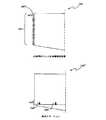
移送ステーション143は、好ましくはFOUPの下端部に提供されるが、他の実施形態では、FOUPの上端部に、またはFOUPの上端部と下端部の間の選択された点に配置することができることを理解されたい。さらに別の実施形態では、移送ステーション143は、処理システム内の別の位置に、例えばFOUP内ではなく固定位置に配置することができる。例えば、図10A〜10Cは、2つの例示代替構成と共に、FOUP100に関する上述の構成を概略的に例示する。
【0053】
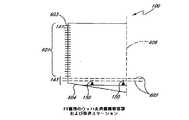
図10Aは、図4〜6に関して上述した構成を例示している。参照番号601は、FOUP100内のウェハ支持機構および/またはウェハに関する全ての格納収容部141を示す。総計23本のストライプ603が示されており、各ストライプ603のすぐ上の空間が、23箇所の格納収納部141の1つを表す。参照番号143が移送ステーションを示す。2つのライン602が、ウェハ支持機構140およびウェハ160のロボット移送に必要な支持ピン150の上の空間を示す。格納収容部141の数を最大にするために、FOUP100の底部での移送ステーション143のピン150は、わずかに外方向にシフトされ、それにより移送ステーション143は、ピン150上にウェハ支持機構140およびウェハ160を収容することができる一方、下側壁604に沿って下方向にシフトすることができる(図6Aおよび6B)。したがって、支持機構140が格納収容部141(図4)内に配置されたときにウェハ支持機構140の穴142と同軸に位置合わせされたピン150に対して、この構成でのピン150は、FOUP100の開口606の方向で外方向にシフトされる。そのような構成では、移送ステーション143でピン150に位置するウェハ支持機構160が、FOUP100から突き出る(図4)。
【0054】
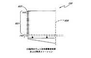
図10Bでは、ウェハ支持機構収容部141の数が21に減り、各ストライプ603のすぐ上の空間が、21箇所の格納収容部141の1つを表す。格納収容部141の数を低減することにより、移送ステーション143を、図10Aに例示される構成に関して内側にシフトすることができ、それにより格納収容部141と同軸に位置合わせして配置することができる。この構成では、ウェハ支持機構140が移送ステーション143に配置されたとき、FOUP100のドア(図示せず)を閉じることができる。
【0055】
図10Cでは、格納機能と移送機能が完全に分離されている。格納収容部141は、1つのFOUP100内に含まれ、移送ステーション143は、FOUP100から完全に離れた個別ステーション100’内に形成される。
【0056】
移送ステーション143を含むFOUPの内部空間内に入る格納収容部141の総数は、利用可能な空間および補助移送ステーション機器によってのみ制限されることを理解されたい。図10A〜10Cに例示される構成では、この数は、0(図10Cのステーション100’の構成)から約23(図10AのFOUP100の構成)の範囲にすることができる。しかし、FOUPの内部空間が増減する場合、例えばFOUPの高さが増減する場合、FOUPは、より多数の、またはより少数の格納収容部141に適合することができる。その結果、例示されたFOUPがウェハ支持機構140に関する特定数の収容部141を提供する一方で、本明細書における教示に従って形成されたカセット内に装填されるウェハ160およびウェハ支持機構140の総数は、本発明の教示によって制限されず、変えることができることを理解されたい。他の実施形態では、ウェハ160およびウェハ支持機構140の数は、25または50、あるいは処理システムによって収容することができる任意の数にすることができる。さらに、他の実施形態では、必要であれば複数のウェハ支持機構140をFOUP内で提供することができる。
【0057】
移送ステーション143内でウェハ160を支持するために支持ピン150が穴を通過することができるように、かつ格納収容部141内で支持ピン150が(典型的には支持リッジ134によって)表面132上にウェハ支持機構140をロックすることができるように同じ穴142(図4)が例示されているが、これらの各位置で、これらの各機能に個別の穴および/または溝を提供することができることも理解されたい。さらに、他の実施形態では、移送ステーション143での支持構造の様々なセットを使用して、それぞれウェハ支持機構140およびウェハ160を支持することができる。例えば、ピン150を使用してウェハ160のみを支持することができ、その一方で、ウェハ支持機構140を、他の支持構造、例えばピン150とは異なる一組のピンによって支持することができる。
【0058】
さらに、ウェハ支持機構140に穴142などの穴を設ける必要はない。例えば、別の実施形態では、ウェハ支持機構140を下面で支持することができ、エンドエフェクタ154の移動が妨げられない限り、ウェハ160を、環状ウェハ支持機構140(例えば図6Bを参照のこと)の中心の開いた領域でピンなどの持上げ構造の上に支持することができる。そのような場合、ウェハ支持機構140に穴142を設ける必要がない。
【0059】
好ましくは、ウェハ支持機構140は石英からなる。別の好ましい実施形態では、高温でのウェハ処理に関連して使用される場合、ウェハ支持機構140は、好ましくは、高温抵抗性をもち、高純度で利用可能な材料から形成される。炭化珪素(SiC)が、そのような材料の一例である。非常に高温での処理の場合、ウェハ支持機構に関する好ましいSiC材料は、いわゆる「フリー・スタンディング」CVD SiCである。これは、はじめは支持材料上に付着され、しかし支持材料の除去を可能にするのに十分な厚さを有するSiCコーティングである。当技術分野で知られているように、支持材料は例えばグラファイトであってよい。「フリー・スタンディング」CVD SiCを有する構造を形成する例示的な方法は、1990年12月18日にMillerに付与された米国特許第4978567号に開示されており、その開示を参照により本明細書に組み込む。
【0060】
有利には、上述したように、好ましい実施形態で、ウェハ160およびウェハ支持機構140を、標準的な炉と共に使用することができるFOUP100などカセット内に格納することができる。したがって、標準のウェハ取扱いロボットを備える標準的な炉は、ハードウェアの大幅な変化を必要とせず、これらの好ましい実施形態に関連して処理を行うように簡単に適合させることができる。さらに、有利には、同時に移送ステーション143を収容する特別なFOUP100内にウェハ支持機構140を提供することは、装填および装填解除中のウェハ支持機構140の移動を最小限に抑えるので特に効率が良い。さらに、ウェハ支持機構140の格納および輸送のためにFOUP100を使用することは、洗浄機器など、FOUPインターフェースを備える他の機器への簡単なアクセスを可能にする。
【0061】
さらに、ウェハ支持機構140を取外し可能にして標準的な設計のスロット付きカセット内に配置することは、ウェハ支持機構140の形状を簡単にし、製造を容易にする。
【0062】
本発明の範囲を逸脱することなく上述したプロセスおよび装置に様々な省略、追加、および修正を加えることができることを当業者は理解されよう。例えば、本明細書で説明した移送ステーションの態様は、開いたカセット内で提供することができ、またはカセットに関連付けられていない個別ステーション内で提供することができる。さらに、様々な構成で、装填解除中にウェハ支持機構からウェハを分離するため、または装填中にウェハ支持機構にウェハを接合するための機構は、例えば、ピン、様々なエンドエフェクトなどの様々なセットまたは向きを使用して、様々な構成を取ることができる。そのような修正および変形は全て、頭記の特許請求の範囲によって定義された本発明の範囲に入るものと意図されている。
【図面の簡単な説明】
【図1】本発明の好ましい実施形態によるウェハのバッチの処理を例示する流れ図である。
【図2】本発明の好ましい実施形態と共に使用するための例示ウェハ処理システムの斜視図である。
【図3】図2のシステムの概略平面図である。
【図4】移送ステーションを備え、本発明の好ましい実施形態に従って構成されたウェハ支持機構格納前開き一体形ポッド(FOUP)の断面図である。
【図5A】FOUPドアが閉じた状態で示された図4の線5−5に沿って取られた図4のウェハ支持機構格納FOUPと、本発明の1つの好ましい実施形態によるウェハ支持機構との断面上面図である。
【図5B】FOUPドアが閉じた状態で示された図4の線5−5に沿って取られた図4のウェハ支持機構格納FOUPと、本発明の別の好ましい実施形態によるウェハ支持機構との断面上面図である。
【図6A】図5Aのウェハ支持機構を保持する移送ステーションを示す、図4の線6−6に沿って取られた図4のウェハ支持機構格納FOUPの断面上面図である。
【図6B】図5Bのウェハ支持機構を保持する移送ステーションを示す、図4の線6−6に沿って取られた図4のウェハ支持機構格納FOUPの断面上面図である。
【図7】本発明の好ましい実施形態と共に使用するための例示縁部支持エンドエフェクタの断面図である。
【図8】本発明の好ましい実施形態と共に使用される例示接触エンドエフェクタの上面図である。
【図9A】本発明の好ましい実施形態によるウェハ支持機構上に支持されたウェハの斜視図である。
【図9B】図9Aのウェハおよびウェハ支持機構の断面図である。
【図10A】本発明の好ましい実施形態によるFOUPに関する例示的な構成を示す概略図である。
【図10B】本発明の好ましい実施形態によるFOUPに関する別の例示的な構成を示す概略図である。
【図10C】本発明の好ましい実施形態によるFOUPに関するさらに別の例示的な構成を示す概略図である。
【符号の説明】
30 ウェハ処理システム
32 ハウジング
33、34、35 隔壁
36、37 垂直炉
38 カセットストア
40 カセット
42 ウェハ支持ホルダ
44 挿入アーム
46 移送アーム
47 支持表面
51 処理領域
52 ウェハ取扱いセクション
53 カセット移送セクション
54 ウェハ取扱いデバイス
100 FOUP
140、160 ウェハ支持機構
141 格納収容部
142 穴
143 移送ステーション
150 ピン
160 ウェハ[0001]
BACKGROUND OF THE INVENTION
The present invention relates generally to semiconductor manufacturing, and more particularly to a method and apparatus for transporting and supporting wafers for batch processing in a furnace.
[0002]
[Prior art]
Thermal related complexity can prevent the use of a typical wafer boat to handle or process batches of wafers at very high temperatures in a furnace, for example, at temperatures up to about 1350 ° C. There is sex. For example, in a general wafer boat, wafers can be supported only at the edge. In such a support scheme, the mechanical strength of the wafer may be reduced at very high temperatures, and the weight of the wafer itself can cause plastic deformation of the wafer at very high temperatures.
[0003]
Other available wafer boat wafer support mechanisms are described in US Pat. Patent Document 1 relates to a wafer boat having a wafer support mechanism having a plurality of inner extending arms for supporting wafers at a plurality of inner positions. Patent Document 2 relates to a wafer boat that supports a wafer at a central position using the entire circumference of a ring support mechanism. However, the support mechanisms on these wafer boards still do not have sufficient support to prevent plastic deformation of the wafer and the resulting crystallographic slip. In order to prevent slipping, the wafer needs to be supported over a substantial portion of the bottom region.
[0004]
Wafer support mechanisms that meet this criteria are known for single wafer systems. In such systems, a susceptor that supports the wafer over the entire bottom area and a support ring that forms a complete circle to support the wafer at the periphery are known in the prior art. However, special measures are required to place the wafer on such a susceptor or to separate the wafer from the susceptor.
[0005]
In particular, in such single wafer systems, when using prior art robot end effectors, access to the wafer is usually made from the bottom, the susceptor stays in place inside the process chamber, the wafers are loaded in series, Unloaded. Generally, a robot end effector places a wafer on a movable pin at a level above the susceptor, and the wafer is spaced well above the susceptor so that the robot end effector contacts the wafer or susceptor. Allow sufficient clearance to pull out the robot end effector without. After drawing, the pins move downward to lower the wafer to the susceptor. To unload the wafer, the reverse of these steps is performed. While such wafer loading and support systems are suitable for single wafer processing, they are not easily applicable to batch processing systems. This is unacceptable because, if possible, among other things, every processing position must have movable pins and associated hardware and control systems for moving these pins. It is complicated and difficult to handle.
[0006]
[Patent Document 1]
US Pat. No. 5,865,321
[Patent Document 2]
US Pat. No. 5,820,367
[0007]
[Patent Document 3]
U.S. Pat. No. 4,407,654
[Patent Document 4]
U.S. Pat. No. 4,770,590
[Patent Document 5]
US Pat. No. 5,161,047
[Patent Document 6]
US Pat. No. 5,192,371
[Patent Document 7]
US Pat. No. 5,219,079
[Patent Document 8]
US Pat. No. 5,310,339
[Patent Document 9]
US Pat. No. 5,316,472
[Patent Document 10]
US Pat. No. 5,334,257
[Patent Document 11]
US Pat. No. 5,407,449
[Patent Document 12]
US Pat. No. 5,482,558
[Patent Document 13]
US Pat. No. 5,482,559
[Patent Document 14]
US Pat. No. 5,492,229
[Patent Document 15]
US Pat. No. 5,556,147
[Patent Document 16]
US Pat. No. 5,556,275
[Patent Document 17]
US Pat. No. 5,858,103
[Patent Document 18]
US Pat. No. 5,897,311
[Patent Document 19]
US Pat. No. 5,931,666
[Patent Document 20]
US Pat. No. 6,099,302
[Patent Document 21]
US Pat. No. 6,203,617
[Patent Document 22]
US Pat. No. 6,287,112
[Patent Document 23]
US Pat. No. 6,321,680
[Patent Document 24]
US Pat. No. 6,341,935
[Patent Document 25]
US Pat. No. 6,361,313
[Patent Document 26]
US Pat. No. 6,390,753
[Patent Document 27]
US Pat. No. 6,464,445
[Patent Document 28]
European Patent Application No. 86308980.1
[Patent Document 29]
International Publication No. 00/68797 Pamphlet
[Patent Document 30]
JP 63-10225 A
[0008]
[Problems to be solved by the invention]
Accordingly, it is an object of the present invention to provide a wafer support system that provides, among other things, a support mechanism for the wafer over a substantial portion of the bottom region and allows for efficient loading and unloading of the wafer for processing in the process chamber. To provide to the wafer boat.
[0009]
[Means for Solving the Problems]
According to one preferred embodiment of the present invention, a method for semiconductor processing is provided. The method includes the steps of: placing a wafer on a wafer support mechanism; then, transporting the wafer into the wafer boat in a state of being placed on the wafer support mechanism; and Subjecting the wafer to a semiconductor manufacturing process in a state of being disposed thereon.
[0010]
According to another preferred embodiment, a method for handling a wafer and wafer support mechanism for processing is provided. The method includes loading a wafer onto a wafer support mechanism in a transfer station, transporting the wafer from the transfer station into a process chamber, and subjecting the wafer to a semiconductor manufacturing process in the process chamber. . During transport of the wafer into the process chamber and subjecting the wafer to a semiconductor manufacturing process, the wafer is placed on a wafer support mechanism.
[0011]
According to yet another preferred embodiment, a system for processing a substrate is provided. The system includes a plurality of substrate support mechanisms for supporting a plurality of substrates.
The substrate support mechanism supports the entire periphery of the substrate, is held in the substrate support holder, and can be detached from the substrate support holder. The process chamber contains a substrate support holder during substrate processing. The system also includes a substrate loading station that is configured to load a substrate on the substrate support mechanism, different from the substrate support holder.
[0012]
According to another preferred embodiment, a semiconductor wafer cassette is provided. The cassette contains a wafer loading station configured to load wafers onto the wafer support mechanism.
[0013]
The present invention will be better understood from the following detailed description of the preferred embodiment, which is intended to illustrate the invention and not to limit it, and to the accompanying drawings.
[0014]
DETAILED DESCRIPTION OF THE INVENTION
Preferred embodiments of the present invention will be described below with reference to the drawings.
[0015]
In accordance with a preferred embodiment of the present invention, a wafer support mechanism is provided for supporting a wafer during a semiconductor manufacturing process. The wafer support mechanism can be detachably stored in the storage accommodating portion of the wafer support holder. The wafer support holder is similar to a standard wafer boat used for semiconductor processing and holds the wafer and wafer support mechanism during processing in the furnace. The wafer support mechanism may also be removably stored in a storage receptacle of a wafer processing cassette, such as a front-opening integrated pod (FOUP) that is adapted to receive a wafer support mechanism of slightly different dimensions than the wafer. it can. The wafer support mechanism preferably supports the wafer over the entire periphery of the wafer, and in this case, desirably, the wafer support mechanism has a higher hoop strength compared to a support mechanism that does not extend around the entire periphery of the wafer. . More preferably, the wafer support mechanism supports a substantial portion of the wafer. In one embodiment, the support mechanism can comprise a plate of material that can support the entire bottom surface of the wafer. In other embodiments, the wafer support mechanism can be ring-shaped. In supporting a “substantial portion” of the wafer, the wafer support mechanism covers more than about 10%, preferably more than about 50%, more preferably more than about 90% of the bottom surface of the wafer. So that it extends under the wafer.
[0016]
In addition to the wafer support mechanism according to a preferred embodiment of the present invention, a transfer or loading station is also provided for placing the wafer on the wafer support mechanism and for removing the wafer from the wafer support mechanism. The transfer station comprises a housing for a wafer support mechanism at a first level and a housing for a wafer at a second level above the first level. During loading, initially the wafer and wafer support mechanism at the second and first levels, respectively, are contacted. Upon contact, the wafer is placed on the wafer support mechanism. During unloading, initially the wafer at the same level and the wafer support mechanism are separated and are located at the second and first levels, respectively.
[0017]
A flowchart of an exemplary procedure for loading and processing a batch of wafers according to a preferred embodiment of the present invention is provided schematically in FIG. As indicated by
[0018]
The wafer is also transported to the transfer station, as indicated by
[0019]
The wafer is then placed on the wafer support mechanism, still in the transfer station, as indicated by
[0020]
In the step indicated by
[0021]
As indicated by
[0022]
The wafer support mechanism and wafer transfer into and out of the transfer station are preferably performed using the same robot and the same end effector. However, it should be understood that various robots and / or various end effectors may be used in other configurations to move the wafer support mechanism and wafer. In particular, depending on the wafer support mechanism used, the robot end effector can also be an edge support end effector that contacts both the wafer support mechanism and the wafer at the edge. A more traditional end effector that contacts both of the wafers can also be a combination of these two end effectors, for example, an end effector that contacts the wafer support mechanism at the edge and contacts the wafer toward the center of the bottom surface. You can also More generally, the end effector can be any end effector suitable for holding the wafer support mechanism and the wafer and performing the operations described herein. For example, an edge support end effector is particularly suitable for a ring-shaped wafer support mechanism, while a wafer support mechanism that is a plate supports a wafer at the edge of the wafer support mechanism or at a more central region of the bottom surface of the wafer support mechanism. It can be held using an end effector that contacts the mechanism. Exemplary end effectors include US Provisional Patent Application 60/377904 filed May 2, 2002, and the corresponding “TWO LEVEL END EFFECTOR” filed February 5, 2003 by den Hartog. No. 10/361480, which is hereby incorporated by reference, the disclosures of which are hereby incorporated by reference.
[0023]
The wafer support mechanism that supports the wafer preferably comprises a circular plate, ie, a structure that supports the entire bottom region of the wafer disposed thereon (see FIGS. 5A and 6A, and the corresponding text below). ). The wafer support mechanism can also be in the shape of a ring, i.e., a centered structure (see FIGS. 5B and 6B, and the corresponding text below). The support “ring” can have a circular shape, but need not be circular, and can be, for example, hexagonal or even square as long as the associated device is configured to accept the shape.
[0024]
In one embodiment, the wafer support mechanism can remain permanently in the processing system. For example, it can be stored in a wafer support holder before and after processing. In another embodiment, the wafer support mechanism is stored and supplied within the processing system in a cassette, and more particularly in a FOUP adapted to receive the wafer support mechanism. This adaptation only requires that the support frame for holding the wafer support mechanism inside the FOUP changes from the standard FOUP configuration. Therefore, the outer surface of the FOUP can maintain its standard configuration. The wafer support mechanism is configured to support a 300 mm wafer and therefore preferably has a diameter that is slightly larger than the diameter of the 300 mm wafer.
[0025]
Further, in one preferred embodiment, a transfer station is provided as part of the FOUP that holds the wafer support mechanism. These adapted FOUPs can be coupled to the processing system via a commercial FOUP receiving station with a FOUP door opener. This embodiment is therefore particularly well adapted to retrofit existing systems. Further, the transfer station can be located at any point between the upper and lower ends of the FOUP, or at either the upper or lower end. The transfer station is preferably located at the lower end of the FOUP.
[0026]
Preferably, the wafer is also supplied to the processing system in a cassette. For a wafer having a diameter of 300 mm, a standard FOUP preferably serves as the cassette used to provide the wafer to the processing system. The FOUP connects to a FOUP station that includes a FOUP door opener provided in the processing system. Thus, in another embodiment, a FOUP that stores a wafer can also include a transfer station, just as a FOUP that stores a wafer support mechanism can include a transfer station. Advantageously, when used in a processing system where the wafer support mechanism remains permanently in the processing system, such a FOUP does not include the need to significantly retrofit individual processing stations to the processing system, for example. In yet another embodiment, a transfer station can be present in the structure regardless of whether the FOUP stores a wafer or a wafer support mechanism.
[0027]
Within the transfer station, the wafer and wafer support mechanism receptacle within the transfer station can comprise various types of support structures used to load and unload wafers onto the wafer support mechanism. Thus, the placement of the wafer on the wafer support mechanism can be accomplished in several ways. For example, in one embodiment, the support structure for the wafer support mechanism can be movable in the vertical direction while the wafer remains stationary. In another embodiment, the support structure for the wafer can be movable vertically and the wafer support mechanism remains stationary. In yet another embodiment, both the support mechanism for the wafer and the support structure for the wafer support mechanism are movable. For example, after placing the wafer support mechanism and the wafer in the storage receptacle, the support structure for the wafer can be moved to move toward the wafer support mechanism until the wafer is positioned on the wafer support mechanism ( Or vice versa, or both the wafer and the wafer support mechanism can move). The wafer support mechanism preferably includes notches (eg, through holes) to allow vertical movement of the support structure and the wafer independently of the wafer support mechanism itself.
[0028]
In another particularly simple embodiment, all support structures in the transfer station are stationary. Vertical movement for placing the wafer on the wafer support mechanism is performed by a robot that transports the wafer support mechanism upward so as to contact the wafer. Thus, the preferred embodiment can advantageously provide the wafer to the process chamber on a wafer support mechanism that supports a substantial portion of the bottom surface region of the wafer, including the entire periphery of the wafer.
[0029]
Reference is now made to the drawings. Like reference numerals refer to like parts throughout the drawings.
[0030]
With reference to FIGS. 2 and 3, an exemplary wafer processing system including a process chamber is illustrated and generally indicated by
[0031]
Wafers are supplied into a
[0032]
The rotatable cassette transfer platform 60 is configured such that the
After placing the cassette relative to the
[0033]
A
[0034]
Obviously, if a transfer station is not included within the FOUP or
In such an embodiment, the two rotatable cassette platforms 60 face both FOUPs (not shown), thereby opening the FOUPs simultaneously with respect to the
[0035]
After loading of the wafer into the
[0036]
Multiple wafers can be processed as follows. An operator schematically shown in FIG. 2 introduces
[0037]
The
[0038]
As described above, the wafer support mechanism can be provided to the processing system in a cassette such as a closeable FOUP. Referring now to FIG. 4, a FOUP according to a preferred embodiment of the present invention is indicated generally by the
[0039]
A
[0040]
A vertically extending
[0041]
It should be understood that 25
[0042]
In order to place the
[0043]
As described above, the position of the
[0044]
After the
[0045]
After the
[0046]
5A and 5B illustrate cross-sectional top views of the
[0047]
6A and 6B illustrate cross-sectional top views of
[0048]
In each of FIGS. 6A and 6B, the
[0049]
A wafer support mechanism and / or a particularly simple edge support end effector for transporting a wafer is illustrated in FIG. The
[0050]
If
[0051]
9A and 9B separately show a perspective view and a cross-sectional view, respectively, of a
The figures are not necessarily drawn to scale, so that, for example, the relative thickness of
[0052]
The
[0053]
FIG. 10A illustrates the configuration described above with respect to FIGS.
[0054]
In FIG. 10B, the number of wafer support mechanism accommodation parts 141 is reduced to 21, and the space immediately above each
[0055]
In FIG. 10C, the storage function and the transport function are completely separated. The storage container 141 is included in one
[0056]
It should be understood that the total number of storage receptacles 141 that fall within the interior space of the FOUP that includes the
[0057]
Support pins 150 can pass through the holes to support
[0058]
Further, it is not necessary to provide holes such as the
[0059]
Preferably, the
[0060]
Advantageously, as described above, in a preferred embodiment,
[0061]
Further, detaching the
[0062]
Those skilled in the art will recognize that various omissions, additions, and modifications may be made to the processes and apparatus described above without departing from the scope of the invention. For example, the transfer station aspects described herein can be provided in an open cassette or can be provided in a separate station not associated with the cassette. In addition, in various configurations, mechanisms for separating the wafer from the wafer support mechanism during unloading or bonding the wafer to the wafer support mechanism during loading can include a variety of pins, various end effects, etc. A set or orientation can be used to take various configurations. All such modifications and variations are intended to fall within the scope of the invention as defined by the appended claims.
[Brief description of the drawings]
FIG. 1 is a flow diagram illustrating the processing of a batch of wafers according to a preferred embodiment of the present invention.
FIG. 2 is a perspective view of an exemplary wafer processing system for use with a preferred embodiment of the present invention.
FIG. 3 is a schematic plan view of the system of FIG.
FIG. 4 is a cross-sectional view of a wafer support mechanism open front integral pod (FOUP) comprising a transfer station and constructed in accordance with a preferred embodiment of the present invention.
5A shows the wafer support mechanism storage FOUP of FIG. 4 taken along line 5-5 of FIG. 4 with the FOUP door closed, and a wafer support mechanism according to one preferred embodiment of the present invention. FIG.
5B shows the wafer support mechanism storage FOUP of FIG. 4 taken along line 5-5 of FIG. 4 with the FOUP door closed, and a wafer support mechanism according to another preferred embodiment of the present invention. FIG.
6A is a cross-sectional top view of the wafer support mechanism storage FOUP of FIG. 4 taken along line 6-6 of FIG. 4, showing the transfer station holding the wafer support mechanism of FIG. 5A.
6B is a cross-sectional top view of the wafer support mechanism storage FOUP of FIG. 4 taken along line 6-6 of FIG. 4, showing the transfer station holding the wafer support mechanism of FIG. 5B.
FIG. 7 is a cross-sectional view of an exemplary edge support end effector for use with a preferred embodiment of the present invention.
FIG. 8 is a top view of an exemplary contact end effector used with a preferred embodiment of the present invention.
FIG. 9A is a perspective view of a wafer supported on a wafer support mechanism according to a preferred embodiment of the present invention.
9B is a cross-sectional view of the wafer and wafer support mechanism of FIG. 9A.
FIG. 10A is a schematic diagram illustrating an exemplary configuration for a FOUP according to a preferred embodiment of the present invention.
FIG. 10B is a schematic diagram illustrating another exemplary configuration for FOUPs according to a preferred embodiment of the present invention.
FIG. 10C is a schematic diagram illustrating yet another exemplary configuration for FOUPs according to a preferred embodiment of the present invention.
[Explanation of symbols]
30 Wafer processing system
32 Housing
33, 34, 35 Bulkhead
36, 37 Vertical furnace
38 cassette store
40 cassettes
42 Wafer support holder
44 Insertion arm
46 Transfer arm
47 Support surface
51 processing area
52 Wafer Handling Section
53 Cassette transfer section
54 Wafer handling devices
100 FOUP
140, 160 Wafer support mechanism
141 storage accommodation
142 holes
143 Transfer Station
150 pins
160 wafers
Claims (27)
Translated fromJapanese複数の基板を支持するための複数の基板支持機構であって、基板の周縁全体を支持する基板支持機構と、
前記複数の基板支持機構を保持するように構成された基板支持ホルダであって、前記複数の基板支持機構が、基板が前記基板支持機構上に配置されている状態で前記基板支持ホルダから取外し可能である基板支持ホルダと、
基板処理中に前記基板支持ホルダを収容するように構成された反応器と、
前記基板支持機構上に基板を装填するように構成された基板装填ステーションであって、前記基板支持ホルダから離隔されている基板装填ステーションと、を備え、
前記基板装填ステーションはウェハカセットに収容されるシステム。A system for processing a substrate,
A plurality of substrate support mechanisms for supporting a plurality of substrates, the substrate support mechanism supporting the entire periphery of the substrate;
A substrate support holder configured to hold the plurality of substrate support mechanisms, wherein the plurality of substrate support mechanisms are removable from the substrate support holder in a state where the substrate is disposed on the substrate support mechanism. A substrate support holder which is
A reactor configured to accommodate the substrate support holder during substrate processing;
A structured substrate loading station to be loaded with substrate on the substrate support mechanism, anda substrate loading station that is spaced apart from the substrate support holder,
The substrate loading station is housed in a wafer cassette.
前記各基板支持機構格納スロットが、前記基板支持機構を支持するための複数の横方向延在面を備える請求項11に記載のカセット。A plurality of substrate support mechanism storage slots in the cassette;
Eachsubstrate support mechanism storage slots, cassette according to claim 11 comprising a plurality of laterally extending surface for supportingsaid substrate supporting mechanism.
当該突出部は、前記複数の横方向延在面の1つから垂直に延在し、当該横方向延在面まで傾斜して下がる側面を有し、
前記突出部は、前記基板支持機構の穴内に延在し、前記基板支持機構の回転を伴わないように、前記基板装填ステーション内で複数の支持ピンと位置合わせされるように前記基板支持機構の複数の穴に向かう請求項12に記載のカセット。Eachsubstrate support mechanism storage slot further comprises a protrusion,
The projecting portionhas a side surface that extends vertically from one of the plurality of laterally extending surfaces and slopes down to thelaterally extending surface,
The protrusionextends into the hole of the substrate supporting mechanism, a plurality of the substrates so without rotation of the support mechanism, the substrate support mechanism so as to be aligned with a plurality of support pins in the substrate loading station The cassette according to claim 12, which is directed to the hole.
前記基板支持機構は、前記ウェハ支持ピンの複数のフレア付きベース上に位置し、
前記ウェハ支持ピンの上側延在部が、前記穴を通って前記基板支持機構の上に延在する請求項17に記載のカセット。The plurality of holesin the substrate support mechanism are sized and positioned to allow the plurality of wafer support pins to pass through the substrate support mechanism;
The substrate support mechanism is located on a plurality of flared bases of the wafer support pins;
The cassette according to claim 17, wherein an upper extending portion of the wafer support pin extends on the substrate support mechanism through the hole.
前記エンドエフェクタが、前記基板支持機構または前記ウェハに接触せずに延在する請求項18に記載のカセット。The upper extending portion of each of the plurality of wafer support pins,the end effector between the wafer positioned on the substrate support mechanismand the previous SL plurality of upper extension portion located in said plurality of flared base extends Have enough height to be able to
The cassette of claim 18, wherein the end effector extends without contacting the substrate support mechanism or the wafer.
基板支持機構上にウェハを配置するステップと、
前記基板支持機構上に前記ウェハを配置するステップがウェハカセットの内部で実行され、その後、前記ウェハが前記基板支持機構上に配置された状態で、前記基板支持機構のための1つ以上の収容部を備えるウェハボート内に前記基板支持機構を輸送するステップと、
前記ウェハボート内で、前記ウェハが前記基板支持機構上に配置された状態で前記ウェハに半導体製造プロセスを施すステップと、を含む方法。A method for processing a semiconductor comprising:
Placing a wafer on a substrate support mechanism;
Placing the wafer on said substrate support mechanism is performed within the wafer cassette, then, in a state in which the wafer is disposed on the substrate support mechanism, one or more accommodating forthe substrate supporting mechanism Transporting the substrate support mechanism into a wafer boat comprising a portion;
Wherein in the wafer boat, wherein said wafer includesthe steps of applying a semiconductor manufacturing process to the wafer in a state of being disposed on the substrate support mechanism.
Applications Claiming Priority (4)
| Application Number | Priority Date | Filing Date | Title |
|---|---|---|---|
| US36512202P | 2002-03-15 | 2002-03-15 | |
| US60/365122 | 2002-03-15 | ||
| US37988502P | 2002-05-10 | 2002-05-10 | |
| US60/379885 | 2002-05-10 |
Publications (3)
| Publication Number | Publication Date |
|---|---|
| JP2003332250A JP2003332250A (en) | 2003-11-21 |
| JP2003332250A5 JP2003332250A5 (en) | 2006-05-11 |
| JP4575647B2true JP4575647B2 (en) | 2010-11-04 |
Family
ID=27767605
Family Applications (1)
| Application Number | Title | Priority Date | Filing Date |
|---|---|---|---|
| JP2003072732AExpired - LifetimeJP4575647B2 (en) | 2002-03-15 | 2003-03-17 | Method and apparatus for batch processing wafers in a furnace |
Country Status (4)
| Country | Link |
|---|---|
| US (1) | US6835039B2 (en) |
| EP (1) | EP1345256B1 (en) |
| JP (1) | JP4575647B2 (en) |
| KR (1) | KR100972346B1 (en) |
Families Citing this family (391)
| Publication number | Priority date | Publication date | Assignee | Title |
|---|---|---|---|---|
| US6776849B2 (en)* | 2002-03-15 | 2004-08-17 | Asm America, Inc. | Wafer holder with peripheral lift ring |
| EP1670534B1 (en)* | 2003-07-02 | 2010-01-27 | Cook Incorporated | Coaxial Catheters |
| US7181132B2 (en) | 2003-08-20 | 2007-02-20 | Asm International N.V. | Method and system for loading substrate supports into a substrate holder |
| US20060065634A1 (en)* | 2004-09-17 | 2006-03-30 | Van Den Berg Jannes R | Low temperature susceptor cleaning |
| US20060060145A1 (en)* | 2004-09-17 | 2006-03-23 | Van Den Berg Jannes R | Susceptor with surface roughness for high temperature substrate processing |
| US8118535B2 (en)* | 2005-05-18 | 2012-02-21 | International Business Machines Corporation | Pod swapping internal to tool run time |
| US7748542B2 (en)* | 2005-08-31 | 2010-07-06 | Applied Materials, Inc. | Batch deposition tool and compressed boat |
| US20080105201A1 (en)* | 2006-11-03 | 2008-05-08 | Applied Materials, Inc. | Substrate support components having quartz contact tips |
| US8180594B2 (en)* | 2007-09-06 | 2012-05-15 | Asm International, N.V. | System and method for automated customizable error diagnostics |
| JP2009087972A (en)* | 2007-09-27 | 2009-04-23 | Tokyo Electron Ltd | Substrate-storing structure and semiconductor manufacturing apparatus |
| US8016592B2 (en)* | 2008-01-01 | 2011-09-13 | Dongguan Anwell Digital Machinery Ltd. | Method and system for thermal processing of objects in chambers |
| JP5338335B2 (en)* | 2008-08-13 | 2013-11-13 | 東京エレクトロン株式会社 | Opening / closing device and probe device of transfer container |
| US10378106B2 (en) | 2008-11-14 | 2019-08-13 | Asm Ip Holding B.V. | Method of forming insulation film by modified PEALD |
| US9394608B2 (en) | 2009-04-06 | 2016-07-19 | Asm America, Inc. | Semiconductor processing reactor and components thereof |
| US8802201B2 (en) | 2009-08-14 | 2014-08-12 | Asm America, Inc. | Systems and methods for thin-film deposition of metal oxides using excited nitrogen-oxygen species |
| US8641350B2 (en)* | 2011-02-18 | 2014-02-04 | Asm International N.V. | Wafer boat assembly, loading apparatus comprising such a wafer boat assembly and method for loading a vertical furnace |
| US9312155B2 (en) | 2011-06-06 | 2016-04-12 | Asm Japan K.K. | High-throughput semiconductor-processing apparatus equipped with multiple dual-chamber modules |
| US10364496B2 (en) | 2011-06-27 | 2019-07-30 | Asm Ip Holding B.V. | Dual section module having shared and unshared mass flow controllers |
| US10854498B2 (en) | 2011-07-15 | 2020-12-01 | Asm Ip Holding B.V. | Wafer-supporting device and method for producing same |
| US20130023129A1 (en) | 2011-07-20 | 2013-01-24 | Asm America, Inc. | Pressure transmitter for a semiconductor processing environment |
| CN102254849A (en)* | 2011-08-08 | 2011-11-23 | 上海宏力半导体制造有限公司 | Loading interlocking device in preparation process of semiconductor device |
| US9017481B1 (en) | 2011-10-28 | 2015-04-28 | Asm America, Inc. | Process feed management for semiconductor substrate processing |
| EP2840599B1 (en)* | 2012-04-16 | 2021-03-31 | Rorze Corporation | Accommodating container and wafer stocker using same |
| US9558931B2 (en) | 2012-07-27 | 2017-01-31 | Asm Ip Holding B.V. | System and method for gas-phase sulfur passivation of a semiconductor surface |
| US9659799B2 (en) | 2012-08-28 | 2017-05-23 | Asm Ip Holding B.V. | Systems and methods for dynamic semiconductor process scheduling |
| US9021985B2 (en) | 2012-09-12 | 2015-05-05 | Asm Ip Holdings B.V. | Process gas management for an inductively-coupled plasma deposition reactor |
| US10714315B2 (en) | 2012-10-12 | 2020-07-14 | Asm Ip Holdings B.V. | Semiconductor reaction chamber showerhead |
| US20160376700A1 (en) | 2013-02-01 | 2016-12-29 | Asm Ip Holding B.V. | System for treatment of deposition reactor |
| US9484191B2 (en) | 2013-03-08 | 2016-11-01 | Asm Ip Holding B.V. | Pulsed remote plasma method and system |
| US9589770B2 (en) | 2013-03-08 | 2017-03-07 | Asm Ip Holding B.V. | Method and systems for in-situ formation of intermediate reactive species |
| US9349643B2 (en)* | 2013-04-01 | 2016-05-24 | Brewer Science Inc. | Apparatus and method for thin wafer transfer |
| US8993054B2 (en) | 2013-07-12 | 2015-03-31 | Asm Ip Holding B.V. | Method and system to reduce outgassing in a reaction chamber |
| US9240412B2 (en) | 2013-09-27 | 2016-01-19 | Asm Ip Holding B.V. | Semiconductor structure and device and methods of forming same using selective epitaxial process |
| US9605343B2 (en) | 2013-11-13 | 2017-03-28 | Asm Ip Holding B.V. | Method for forming conformal carbon films, structures conformal carbon film, and system of forming same |
| US10683571B2 (en) | 2014-02-25 | 2020-06-16 | Asm Ip Holding B.V. | Gas supply manifold and method of supplying gases to chamber using same |
| US10167557B2 (en) | 2014-03-18 | 2019-01-01 | Asm Ip Holding B.V. | Gas distribution system, reactor including the system, and methods of using the same |
| US11015245B2 (en) | 2014-03-19 | 2021-05-25 | Asm Ip Holding B.V. | Gas-phase reactor and system having exhaust plenum and components thereof |
| CN104037110B (en)* | 2014-05-20 | 2019-12-06 | 上海申和热磁电子有限公司 | Semiconductor silicon wafer stripping shovel |
| TWI506702B (en)* | 2014-07-28 | 2015-11-01 | Powerchip Technology Corp | Dispatch control method for furnace process |
| US10858737B2 (en) | 2014-07-28 | 2020-12-08 | Asm Ip Holding B.V. | Showerhead assembly and components thereof |
| US9543180B2 (en)* | 2014-08-01 | 2017-01-10 | Asm Ip Holding B.V. | Apparatus and method for transporting wafers between wafer carrier and process tool under vacuum |
| US9890456B2 (en) | 2014-08-21 | 2018-02-13 | Asm Ip Holding B.V. | Method and system for in situ formation of gas-phase compounds |
| US9657845B2 (en) | 2014-10-07 | 2017-05-23 | Asm Ip Holding B.V. | Variable conductance gas distribution apparatus and method |
| US10941490B2 (en) | 2014-10-07 | 2021-03-09 | Asm Ip Holding B.V. | Multiple temperature range susceptor, assembly, reactor and system including the susceptor, and methods of using the same |
| KR102300403B1 (en) | 2014-11-19 | 2021-09-09 | 에이에스엠 아이피 홀딩 비.브이. | Method of depositing thin film |
| KR102263121B1 (en) | 2014-12-22 | 2021-06-09 | 에이에스엠 아이피 홀딩 비.브이. | Semiconductor device and manufacuring method thereof |
| US10529542B2 (en) | 2015-03-11 | 2020-01-07 | Asm Ip Holdings B.V. | Cross-flow reactor and method |
| US10276355B2 (en) | 2015-03-12 | 2019-04-30 | Asm Ip Holding B.V. | Multi-zone reactor, system including the reactor, and method of using the same |
| US10458018B2 (en) | 2015-06-26 | 2019-10-29 | Asm Ip Holding B.V. | Structures including metal carbide material, devices including the structures, and methods of forming same |
| US10600673B2 (en) | 2015-07-07 | 2020-03-24 | Asm Ip Holding B.V. | Magnetic susceptor to baseplate seal |
| US10043661B2 (en) | 2015-07-13 | 2018-08-07 | Asm Ip Holding B.V. | Method for protecting layer by forming hydrocarbon-based extremely thin film |
| US10083836B2 (en) | 2015-07-24 | 2018-09-25 | Asm Ip Holding B.V. | Formation of boron-doped titanium metal films with high work function |
| US10087525B2 (en) | 2015-08-04 | 2018-10-02 | Asm Ip Holding B.V. | Variable gap hard stop design |
| US9647114B2 (en) | 2015-08-14 | 2017-05-09 | Asm Ip Holding B.V. | Methods of forming highly p-type doped germanium tin films and structures and devices including the films |
| CN106469671A (en)* | 2015-08-19 | 2017-03-01 | 英属开曼群岛商精曜有限公司 | Mechanical bearing arm and the method for carrying of wafer |
| US9960072B2 (en) | 2015-09-29 | 2018-05-01 | Asm Ip Holding B.V. | Variable adjustment for precise matching of multiple chamber cavity housings |
| US10211308B2 (en) | 2015-10-21 | 2019-02-19 | Asm Ip Holding B.V. | NbMC layers |
| US10322384B2 (en) | 2015-11-09 | 2019-06-18 | Asm Ip Holding B.V. | Counter flow mixer for process chamber |
| US9627221B1 (en) | 2015-12-28 | 2017-04-18 | Asm Ip Holding B.V. | Continuous process incorporating atomic layer etching |
| US11139308B2 (en) | 2015-12-29 | 2021-10-05 | Asm Ip Holding B.V. | Atomic layer deposition of III-V compounds to form V-NAND devices |
| US10468251B2 (en) | 2016-02-19 | 2019-11-05 | Asm Ip Holding B.V. | Method for forming spacers using silicon nitride film for spacer-defined multiple patterning |
| US10529554B2 (en) | 2016-02-19 | 2020-01-07 | Asm Ip Holding B.V. | Method for forming silicon nitride film selectively on sidewalls or flat surfaces of trenches |
| US10501866B2 (en) | 2016-03-09 | 2019-12-10 | Asm Ip Holding B.V. | Gas distribution apparatus for improved film uniformity in an epitaxial system |
| US10343920B2 (en) | 2016-03-18 | 2019-07-09 | Asm Ip Holding B.V. | Aligned carbon nanotubes |
| US9892913B2 (en) | 2016-03-24 | 2018-02-13 | Asm Ip Holding B.V. | Radial and thickness control via biased multi-port injection settings |
| US10087522B2 (en) | 2016-04-21 | 2018-10-02 | Asm Ip Holding B.V. | Deposition of metal borides |
| US10190213B2 (en) | 2016-04-21 | 2019-01-29 | Asm Ip Holding B.V. | Deposition of metal borides |
| US10865475B2 (en) | 2016-04-21 | 2020-12-15 | Asm Ip Holding B.V. | Deposition of metal borides and silicides |
| US10032628B2 (en) | 2016-05-02 | 2018-07-24 | Asm Ip Holding B.V. | Source/drain performance through conformal solid state doping |
| US10367080B2 (en) | 2016-05-02 | 2019-07-30 | Asm Ip Holding B.V. | Method of forming a germanium oxynitride film |
| KR102592471B1 (en) | 2016-05-17 | 2023-10-20 | 에이에스엠 아이피 홀딩 비.브이. | Method of forming metal interconnection and method of fabricating semiconductor device using the same |
| US11453943B2 (en) | 2016-05-25 | 2022-09-27 | Asm Ip Holding B.V. | Method for forming carbon-containing silicon/metal oxide or nitride film by ALD using silicon precursor and hydrocarbon precursor |
| US10388509B2 (en) | 2016-06-28 | 2019-08-20 | Asm Ip Holding B.V. | Formation of epitaxial layers via dislocation filtering |
| US10612137B2 (en) | 2016-07-08 | 2020-04-07 | Asm Ip Holdings B.V. | Organic reactants for atomic layer deposition |
| US9859151B1 (en) | 2016-07-08 | 2018-01-02 | Asm Ip Holding B.V. | Selective film deposition method to form air gaps |
| US9793135B1 (en) | 2016-07-14 | 2017-10-17 | ASM IP Holding B.V | Method of cyclic dry etching using etchant film |
| US10714385B2 (en) | 2016-07-19 | 2020-07-14 | Asm Ip Holding B.V. | Selective deposition of tungsten |
| KR102354490B1 (en) | 2016-07-27 | 2022-01-21 | 에이에스엠 아이피 홀딩 비.브이. | Method of processing a substrate |
| US9812320B1 (en) | 2016-07-28 | 2017-11-07 | Asm Ip Holding B.V. | Method and apparatus for filling a gap |
| KR102532607B1 (en) | 2016-07-28 | 2023-05-15 | 에이에스엠 아이피 홀딩 비.브이. | Substrate processing apparatus and method of operating the same |
| US10395919B2 (en) | 2016-07-28 | 2019-08-27 | Asm Ip Holding B.V. | Method and apparatus for filling a gap |
| US10177025B2 (en) | 2016-07-28 | 2019-01-08 | Asm Ip Holding B.V. | Method and apparatus for filling a gap |
| US9887082B1 (en) | 2016-07-28 | 2018-02-06 | Asm Ip Holding B.V. | Method and apparatus for filling a gap |
| US10090316B2 (en) | 2016-09-01 | 2018-10-02 | Asm Ip Holding B.V. | 3D stacked multilayer semiconductor memory using doped select transistor channel |
| US10410943B2 (en) | 2016-10-13 | 2019-09-10 | Asm Ip Holding B.V. | Method for passivating a surface of a semiconductor and related systems |
| US10643826B2 (en) | 2016-10-26 | 2020-05-05 | Asm Ip Holdings B.V. | Methods for thermally calibrating reaction chambers |
| US11532757B2 (en) | 2016-10-27 | 2022-12-20 | Asm Ip Holding B.V. | Deposition of charge trapping layers |
| US10643904B2 (en) | 2016-11-01 | 2020-05-05 | Asm Ip Holdings B.V. | Methods for forming a semiconductor device and related semiconductor device structures |
| US10714350B2 (en) | 2016-11-01 | 2020-07-14 | ASM IP Holdings, B.V. | Methods for forming a transition metal niobium nitride film on a substrate by atomic layer deposition and related semiconductor device structures |
| US10229833B2 (en) | 2016-11-01 | 2019-03-12 | Asm Ip Holding B.V. | Methods for forming a transition metal nitride film on a substrate by atomic layer deposition and related semiconductor device structures |
| US10435790B2 (en) | 2016-11-01 | 2019-10-08 | Asm Ip Holding B.V. | Method of subatmospheric plasma-enhanced ALD using capacitively coupled electrodes with narrow gap |
| US10134757B2 (en) | 2016-11-07 | 2018-11-20 | Asm Ip Holding B.V. | Method of processing a substrate and a device manufactured by using the method |
| KR102546317B1 (en) | 2016-11-15 | 2023-06-21 | 에이에스엠 아이피 홀딩 비.브이. | Gas supply unit and substrate processing apparatus including the same |
| US10340135B2 (en) | 2016-11-28 | 2019-07-02 | Asm Ip Holding B.V. | Method of topologically restricted plasma-enhanced cyclic deposition of silicon or metal nitride |
| KR102762543B1 (en) | 2016-12-14 | 2025-02-05 | 에이에스엠 아이피 홀딩 비.브이. | Substrate processing apparatus |
| US11581186B2 (en) | 2016-12-15 | 2023-02-14 | Asm Ip Holding B.V. | Sequential infiltration synthesis apparatus |
| US9916980B1 (en) | 2016-12-15 | 2018-03-13 | Asm Ip Holding B.V. | Method of forming a structure on a substrate |
| US11447861B2 (en) | 2016-12-15 | 2022-09-20 | Asm Ip Holding B.V. | Sequential infiltration synthesis apparatus and a method of forming a patterned structure |
| KR102700194B1 (en) | 2016-12-19 | 2024-08-28 | 에이에스엠 아이피 홀딩 비.브이. | Substrate processing apparatus |
| US10269558B2 (en) | 2016-12-22 | 2019-04-23 | Asm Ip Holding B.V. | Method of forming a structure on a substrate |
| US10867788B2 (en) | 2016-12-28 | 2020-12-15 | Asm Ip Holding B.V. | Method of forming a structure on a substrate |
| US11390950B2 (en) | 2017-01-10 | 2022-07-19 | Asm Ip Holding B.V. | Reactor system and method to reduce residue buildup during a film deposition process |
| US10655221B2 (en) | 2017-02-09 | 2020-05-19 | Asm Ip Holding B.V. | Method for depositing oxide film by thermal ALD and PEALD |
| US10468261B2 (en) | 2017-02-15 | 2019-11-05 | Asm Ip Holding B.V. | Methods for forming a metallic film on a substrate by cyclical deposition and related semiconductor device structures |
| US10283353B2 (en) | 2017-03-29 | 2019-05-07 | Asm Ip Holding B.V. | Method of reforming insulating film deposited on substrate with recess pattern |
| US10529563B2 (en) | 2017-03-29 | 2020-01-07 | Asm Ip Holdings B.V. | Method for forming doped metal oxide films on a substrate by cyclical deposition and related semiconductor device structures |
| US10103040B1 (en) | 2017-03-31 | 2018-10-16 | Asm Ip Holding B.V. | Apparatus and method for manufacturing a semiconductor device |
| USD830981S1 (en) | 2017-04-07 | 2018-10-16 | Asm Ip Holding B.V. | Susceptor for semiconductor substrate processing apparatus |
| KR102457289B1 (en) | 2017-04-25 | 2022-10-21 | 에이에스엠 아이피 홀딩 비.브이. | Method for depositing a thin film and manufacturing a semiconductor device |
| US10770286B2 (en) | 2017-05-08 | 2020-09-08 | Asm Ip Holdings B.V. | Methods for selectively forming a silicon nitride film on a substrate and related semiconductor device structures |
| US10892156B2 (en) | 2017-05-08 | 2021-01-12 | Asm Ip Holding B.V. | Methods for forming a silicon nitride film on a substrate and related semiconductor device structures |
| US10446393B2 (en) | 2017-05-08 | 2019-10-15 | Asm Ip Holding B.V. | Methods for forming silicon-containing epitaxial layers and related semiconductor device structures |
| US10504742B2 (en) | 2017-05-31 | 2019-12-10 | Asm Ip Holding B.V. | Method of atomic layer etching using hydrogen plasma |
| US10886123B2 (en) | 2017-06-02 | 2021-01-05 | Asm Ip Holding B.V. | Methods for forming low temperature semiconductor layers and related semiconductor device structures |
| US12040200B2 (en) | 2017-06-20 | 2024-07-16 | Asm Ip Holding B.V. | Semiconductor processing apparatus and methods for calibrating a semiconductor processing apparatus |
| US11306395B2 (en) | 2017-06-28 | 2022-04-19 | Asm Ip Holding B.V. | Methods for depositing a transition metal nitride film on a substrate by atomic layer deposition and related deposition apparatus |
| US10685834B2 (en) | 2017-07-05 | 2020-06-16 | Asm Ip Holdings B.V. | Methods for forming a silicon germanium tin layer and related semiconductor device structures |
| KR20190009245A (en) | 2017-07-18 | 2019-01-28 | 에이에스엠 아이피 홀딩 비.브이. | Methods for forming a semiconductor device structure and related semiconductor device structures |
| US11374112B2 (en) | 2017-07-19 | 2022-06-28 | Asm Ip Holding B.V. | Method for depositing a group IV semiconductor and related semiconductor device structures |
| US11018002B2 (en) | 2017-07-19 | 2021-05-25 | Asm Ip Holding B.V. | Method for selectively depositing a Group IV semiconductor and related semiconductor device structures |
| US10541333B2 (en) | 2017-07-19 | 2020-01-21 | Asm Ip Holding B.V. | Method for depositing a group IV semiconductor and related semiconductor device structures |
| US10312055B2 (en) | 2017-07-26 | 2019-06-04 | Asm Ip Holding B.V. | Method of depositing film by PEALD using negative bias |
| US10590535B2 (en) | 2017-07-26 | 2020-03-17 | Asm Ip Holdings B.V. | Chemical treatment, deposition and/or infiltration apparatus and method for using the same |
| US10605530B2 (en) | 2017-07-26 | 2020-03-31 | Asm Ip Holding B.V. | Assembly of a liner and a flange for a vertical furnace as well as the liner and the vertical furnace |
| TWI815813B (en) | 2017-08-04 | 2023-09-21 | 荷蘭商Asm智慧財產控股公司 | Showerhead assembly for distributing a gas within a reaction chamber |
| US10692741B2 (en) | 2017-08-08 | 2020-06-23 | Asm Ip Holdings B.V. | Radiation shield |
| US10770336B2 (en) | 2017-08-08 | 2020-09-08 | Asm Ip Holding B.V. | Substrate lift mechanism and reactor including same |
| US11139191B2 (en) | 2017-08-09 | 2021-10-05 | Asm Ip Holding B.V. | Storage apparatus for storing cassettes for substrates and processing apparatus equipped therewith |
| US11769682B2 (en) | 2017-08-09 | 2023-09-26 | Asm Ip Holding B.V. | Storage apparatus for storing cassettes for substrates and processing apparatus equipped therewith |
| US10249524B2 (en) | 2017-08-09 | 2019-04-02 | Asm Ip Holding B.V. | Cassette holder assembly for a substrate cassette and holding member for use in such assembly |
| US10236177B1 (en) | 2017-08-22 | 2019-03-19 | ASM IP Holding B.V.. | Methods for depositing a doped germanium tin semiconductor and related semiconductor device structures |
| USD900036S1 (en) | 2017-08-24 | 2020-10-27 | Asm Ip Holding B.V. | Heater electrical connector and adapter |
| US11830730B2 (en) | 2017-08-29 | 2023-11-28 | Asm Ip Holding B.V. | Layer forming method and apparatus |
| KR102491945B1 (en) | 2017-08-30 | 2023-01-26 | 에이에스엠 아이피 홀딩 비.브이. | Substrate processing apparatus |
| US11295980B2 (en) | 2017-08-30 | 2022-04-05 | Asm Ip Holding B.V. | Methods for depositing a molybdenum metal film over a dielectric surface of a substrate by a cyclical deposition process and related semiconductor device structures |
| US11056344B2 (en) | 2017-08-30 | 2021-07-06 | Asm Ip Holding B.V. | Layer forming method |
| KR102401446B1 (en) | 2017-08-31 | 2022-05-24 | 에이에스엠 아이피 홀딩 비.브이. | Substrate processing apparatus |
| US10607895B2 (en) | 2017-09-18 | 2020-03-31 | Asm Ip Holdings B.V. | Method for forming a semiconductor device structure comprising a gate fill metal |
| KR102630301B1 (en) | 2017-09-21 | 2024-01-29 | 에이에스엠 아이피 홀딩 비.브이. | Method of sequential infiltration synthesis treatment of infiltrateable material and structures and devices formed using same |
| US10844484B2 (en) | 2017-09-22 | 2020-11-24 | Asm Ip Holding B.V. | Apparatus for dispensing a vapor phase reactant to a reaction chamber and related methods |
| US10658205B2 (en) | 2017-09-28 | 2020-05-19 | Asm Ip Holdings B.V. | Chemical dispensing apparatus and methods for dispensing a chemical to a reaction chamber |
| US10403504B2 (en) | 2017-10-05 | 2019-09-03 | Asm Ip Holding B.V. | Method for selectively depositing a metallic film on a substrate |
| US10319588B2 (en) | 2017-10-10 | 2019-06-11 | Asm Ip Holding B.V. | Method for depositing a metal chalcogenide on a substrate by cyclical deposition |
| US10923344B2 (en) | 2017-10-30 | 2021-02-16 | Asm Ip Holding B.V. | Methods for forming a semiconductor structure and related semiconductor structures |
| KR102443047B1 (en) | 2017-11-16 | 2022-09-14 | 에이에스엠 아이피 홀딩 비.브이. | Method of processing a substrate and a device manufactured by the same |
| US10910262B2 (en) | 2017-11-16 | 2021-02-02 | Asm Ip Holding B.V. | Method of selectively depositing a capping layer structure on a semiconductor device structure |
| US11022879B2 (en) | 2017-11-24 | 2021-06-01 | Asm Ip Holding B.V. | Method of forming an enhanced unexposed photoresist layer |
| CN111344522B (en) | 2017-11-27 | 2022-04-12 | 阿斯莫Ip控股公司 | Including clean mini-environment device |
| WO2019103613A1 (en) | 2017-11-27 | 2019-05-31 | Asm Ip Holding B.V. | A storage device for storing wafer cassettes for use with a batch furnace |
| US10290508B1 (en) | 2017-12-05 | 2019-05-14 | Asm Ip Holding B.V. | Method for forming vertical spacers for spacer-defined patterning |
| US10872771B2 (en) | 2018-01-16 | 2020-12-22 | Asm Ip Holding B. V. | Method for depositing a material film on a substrate within a reaction chamber by a cyclical deposition process and related device structures |
| KR102695659B1 (en) | 2018-01-19 | 2024-08-14 | 에이에스엠 아이피 홀딩 비.브이. | Method for depositing a gap filling layer by plasma assisted deposition |
| TWI799494B (en) | 2018-01-19 | 2023-04-21 | 荷蘭商Asm 智慧財產控股公司 | Deposition method |
| USD903477S1 (en) | 2018-01-24 | 2020-12-01 | Asm Ip Holdings B.V. | Metal clamp |
| US11018047B2 (en) | 2018-01-25 | 2021-05-25 | Asm Ip Holding B.V. | Hybrid lift pin |
| USD880437S1 (en) | 2018-02-01 | 2020-04-07 | Asm Ip Holding B.V. | Gas supply plate for semiconductor manufacturing apparatus |
| US10535516B2 (en) | 2018-02-01 | 2020-01-14 | Asm Ip Holdings B.V. | Method for depositing a semiconductor structure on a surface of a substrate and related semiconductor structures |
| US11081345B2 (en) | 2018-02-06 | 2021-08-03 | Asm Ip Holding B.V. | Method of post-deposition treatment for silicon oxide film |
| WO2019158960A1 (en) | 2018-02-14 | 2019-08-22 | Asm Ip Holding B.V. | A method for depositing a ruthenium-containing film on a substrate by a cyclical deposition process |
| US10896820B2 (en) | 2018-02-14 | 2021-01-19 | Asm Ip Holding B.V. | Method for depositing a ruthenium-containing film on a substrate by a cyclical deposition process |
| US10731249B2 (en) | 2018-02-15 | 2020-08-04 | Asm Ip Holding B.V. | Method of forming a transition metal containing film on a substrate by a cyclical deposition process, a method for supplying a transition metal halide compound to a reaction chamber, and related vapor deposition apparatus |
| US10658181B2 (en) | 2018-02-20 | 2020-05-19 | Asm Ip Holding B.V. | Method of spacer-defined direct patterning in semiconductor fabrication |
| KR102636427B1 (en) | 2018-02-20 | 2024-02-13 | 에이에스엠 아이피 홀딩 비.브이. | Substrate processing method and apparatus |
| US10975470B2 (en) | 2018-02-23 | 2021-04-13 | Asm Ip Holding B.V. | Apparatus for detecting or monitoring for a chemical precursor in a high temperature environment |
| US11473195B2 (en) | 2018-03-01 | 2022-10-18 | Asm Ip Holding B.V. | Semiconductor processing apparatus and a method for processing a substrate |
| US11629406B2 (en) | 2018-03-09 | 2023-04-18 | Asm Ip Holding B.V. | Semiconductor processing apparatus comprising one or more pyrometers for measuring a temperature of a substrate during transfer of the substrate |
| US11114283B2 (en) | 2018-03-16 | 2021-09-07 | Asm Ip Holding B.V. | Reactor, system including the reactor, and methods of manufacturing and using same |
| KR102646467B1 (en) | 2018-03-27 | 2024-03-11 | 에이에스엠 아이피 홀딩 비.브이. | Method of forming an electrode on a substrate and a semiconductor device structure including an electrode |
| US10510536B2 (en) | 2018-03-29 | 2019-12-17 | Asm Ip Holding B.V. | Method of depositing a co-doped polysilicon film on a surface of a substrate within a reaction chamber |
| US11088002B2 (en) | 2018-03-29 | 2021-08-10 | Asm Ip Holding B.V. | Substrate rack and a substrate processing system and method |
| US11230766B2 (en) | 2018-03-29 | 2022-01-25 | Asm Ip Holding B.V. | Substrate processing apparatus and method |
| KR102501472B1 (en) | 2018-03-30 | 2023-02-20 | 에이에스엠 아이피 홀딩 비.브이. | Substrate processing method |
| KR102600229B1 (en) | 2018-04-09 | 2023-11-10 | 에이에스엠 아이피 홀딩 비.브이. | Substrate supporting device, substrate processing apparatus including the same and substrate processing method |
| US12025484B2 (en) | 2018-05-08 | 2024-07-02 | Asm Ip Holding B.V. | Thin film forming method |
| TWI811348B (en) | 2018-05-08 | 2023-08-11 | 荷蘭商Asm 智慧財產控股公司 | Methods for depositing an oxide film on a substrate by a cyclical deposition process and related device structures |
| US12272527B2 (en) | 2018-05-09 | 2025-04-08 | Asm Ip Holding B.V. | Apparatus for use with hydrogen radicals and method of using same |
| KR20190129718A (en) | 2018-05-11 | 2019-11-20 | 에이에스엠 아이피 홀딩 비.브이. | Methods for forming a doped metal carbide film on a substrate and related semiconductor device structures |
| KR102596988B1 (en) | 2018-05-28 | 2023-10-31 | 에이에스엠 아이피 홀딩 비.브이. | Method of processing a substrate and a device manufactured by the same |
| US11718913B2 (en) | 2018-06-04 | 2023-08-08 | Asm Ip Holding B.V. | Gas distribution system and reactor system including same |
| TWI840362B (en) | 2018-06-04 | 2024-05-01 | 荷蘭商Asm Ip私人控股有限公司 | Wafer handling chamber with moisture reduction |
| US11286562B2 (en) | 2018-06-08 | 2022-03-29 | Asm Ip Holding B.V. | Gas-phase chemical reactor and method of using same |
| US10797133B2 (en) | 2018-06-21 | 2020-10-06 | Asm Ip Holding B.V. | Method for depositing a phosphorus doped silicon arsenide film and related semiconductor device structures |
| KR102568797B1 (en) | 2018-06-21 | 2023-08-21 | 에이에스엠 아이피 홀딩 비.브이. | Substrate processing system |
| TWI873894B (en) | 2018-06-27 | 2025-02-21 | 荷蘭商Asm Ip私人控股有限公司 | Cyclic deposition methods for forming metal-containing material and films and structures including the metal-containing material |
| KR102854019B1 (en) | 2018-06-27 | 2025-09-02 | 에이에스엠 아이피 홀딩 비.브이. | Periodic deposition method for forming a metal-containing material and films and structures comprising the metal-containing material |
| KR102686758B1 (en) | 2018-06-29 | 2024-07-18 | 에이에스엠 아이피 홀딩 비.브이. | Method for depositing a thin film and manufacturing a semiconductor device |
| US10612136B2 (en) | 2018-06-29 | 2020-04-07 | ASM IP Holding, B.V. | Temperature-controlled flange and reactor system including same |
| US10755922B2 (en) | 2018-07-03 | 2020-08-25 | Asm Ip Holding B.V. | Method for depositing silicon-free carbon-containing film as gap-fill layer by pulse plasma-assisted deposition |
| US10388513B1 (en) | 2018-07-03 | 2019-08-20 | Asm Ip Holding B.V. | Method for depositing silicon-free carbon-containing film as gap-fill layer by pulse plasma-assisted deposition |
| US10767789B2 (en) | 2018-07-16 | 2020-09-08 | Asm Ip Holding B.V. | Diaphragm valves, valve components, and methods for forming valve components |
| US10483099B1 (en) | 2018-07-26 | 2019-11-19 | Asm Ip Holding B.V. | Method for forming thermally stable organosilicon polymer film |
| US11053591B2 (en) | 2018-08-06 | 2021-07-06 | Asm Ip Holding B.V. | Multi-port gas injection system and reactor system including same |
| US10883175B2 (en) | 2018-08-09 | 2021-01-05 | Asm Ip Holding B.V. | Vertical furnace for processing substrates and a liner for use therein |
| US10829852B2 (en) | 2018-08-16 | 2020-11-10 | Asm Ip Holding B.V. | Gas distribution device for a wafer processing apparatus |
| US11430674B2 (en) | 2018-08-22 | 2022-08-30 | Asm Ip Holding B.V. | Sensor array, apparatus for dispensing a vapor phase reactant to a reaction chamber and related methods |
| US11024523B2 (en) | 2018-09-11 | 2021-06-01 | Asm Ip Holding B.V. | Substrate processing apparatus and method |
| KR102707956B1 (en) | 2018-09-11 | 2024-09-19 | 에이에스엠 아이피 홀딩 비.브이. | Method for deposition of a thin film |
| US11049751B2 (en) | 2018-09-14 | 2021-06-29 | Asm Ip Holding B.V. | Cassette supply system to store and handle cassettes and processing apparatus equipped therewith |
| CN110970344B (en) | 2018-10-01 | 2024-10-25 | Asmip控股有限公司 | Substrate holding apparatus, system comprising the same and method of using the same |
| US11232963B2 (en) | 2018-10-03 | 2022-01-25 | Asm Ip Holding B.V. | Substrate processing apparatus and method |
| KR102592699B1 (en) | 2018-10-08 | 2023-10-23 | 에이에스엠 아이피 홀딩 비.브이. | Substrate support unit and apparatuses for depositing thin film and processing the substrate including the same |
| US10847365B2 (en) | 2018-10-11 | 2020-11-24 | Asm Ip Holding B.V. | Method of forming conformal silicon carbide film by cyclic CVD |
| US10811256B2 (en) | 2018-10-16 | 2020-10-20 | Asm Ip Holding B.V. | Method for etching a carbon-containing feature |
| KR102546322B1 (en) | 2018-10-19 | 2023-06-21 | 에이에스엠 아이피 홀딩 비.브이. | Substrate processing apparatus and substrate processing method |
| KR102605121B1 (en) | 2018-10-19 | 2023-11-23 | 에이에스엠 아이피 홀딩 비.브이. | Substrate processing apparatus and substrate processing method |
| USD948463S1 (en) | 2018-10-24 | 2022-04-12 | Asm Ip Holding B.V. | Susceptor for semiconductor substrate supporting apparatus |
| US10381219B1 (en) | 2018-10-25 | 2019-08-13 | Asm Ip Holding B.V. | Methods for forming a silicon nitride film |
| US12378665B2 (en) | 2018-10-26 | 2025-08-05 | Asm Ip Holding B.V. | High temperature coatings for a preclean and etch apparatus and related methods |
| US11087997B2 (en) | 2018-10-31 | 2021-08-10 | Asm Ip Holding B.V. | Substrate processing apparatus for processing substrates |
| KR102748291B1 (en) | 2018-11-02 | 2024-12-31 | 에이에스엠 아이피 홀딩 비.브이. | Substrate support unit and substrate processing apparatus including the same |
| US11572620B2 (en) | 2018-11-06 | 2023-02-07 | Asm Ip Holding B.V. | Methods for selectively depositing an amorphous silicon film on a substrate |
| US11031242B2 (en) | 2018-11-07 | 2021-06-08 | Asm Ip Holding B.V. | Methods for depositing a boron doped silicon germanium film |
| US10847366B2 (en) | 2018-11-16 | 2020-11-24 | Asm Ip Holding B.V. | Methods for depositing a transition metal chalcogenide film on a substrate by a cyclical deposition process |
| US10818758B2 (en) | 2018-11-16 | 2020-10-27 | Asm Ip Holding B.V. | Methods for forming a metal silicate film on a substrate in a reaction chamber and related semiconductor device structures |
| US10559458B1 (en) | 2018-11-26 | 2020-02-11 | Asm Ip Holding B.V. | Method of forming oxynitride film |
| US12040199B2 (en) | 2018-11-28 | 2024-07-16 | Asm Ip Holding B.V. | Substrate processing apparatus for processing substrates |
| US11217444B2 (en) | 2018-11-30 | 2022-01-04 | Asm Ip Holding B.V. | Method for forming an ultraviolet radiation responsive metal oxide-containing film |
| KR102636428B1 (en) | 2018-12-04 | 2024-02-13 | 에이에스엠 아이피 홀딩 비.브이. | A method for cleaning a substrate processing apparatus |
| US11158513B2 (en) | 2018-12-13 | 2021-10-26 | Asm Ip Holding B.V. | Methods for forming a rhenium-containing film on a substrate by a cyclical deposition process and related semiconductor device structures |
| TWI874340B (en) | 2018-12-14 | 2025-03-01 | 荷蘭商Asm Ip私人控股有限公司 | Method of forming device structure, structure formed by the method and system for performing the method |
| JP7003905B2 (en)* | 2018-12-27 | 2022-01-21 | 株式会社Sumco | Vapor deposition equipment |
| TWI866480B (en) | 2019-01-17 | 2024-12-11 | 荷蘭商Asm Ip 私人控股有限公司 | Methods of forming a transition metal containing film on a substrate by a cyclical deposition process |
| KR102727227B1 (en) | 2019-01-22 | 2024-11-07 | 에이에스엠 아이피 홀딩 비.브이. | Semiconductor processing device |
| CN111524788B (en) | 2019-02-01 | 2023-11-24 | Asm Ip私人控股有限公司 | Method for forming topologically selective films of silicon oxide |
| TWI838458B (en) | 2019-02-20 | 2024-04-11 | 荷蘭商Asm Ip私人控股有限公司 | Apparatus and methods for plug fill deposition in 3-d nand applications |
| TWI845607B (en) | 2019-02-20 | 2024-06-21 | 荷蘭商Asm Ip私人控股有限公司 | Cyclical deposition method and apparatus for filling a recess formed within a substrate surface |
| KR102626263B1 (en) | 2019-02-20 | 2024-01-16 | 에이에스엠 아이피 홀딩 비.브이. | Cyclical deposition method including treatment step and apparatus for same |
| TWI873122B (en) | 2019-02-20 | 2025-02-21 | 荷蘭商Asm Ip私人控股有限公司 | Method of filling a recess formed within a surface of a substrate, semiconductor structure formed according to the method, and semiconductor processing apparatus |
| TWI842826B (en) | 2019-02-22 | 2024-05-21 | 荷蘭商Asm Ip私人控股有限公司 | Substrate processing apparatus and method for processing substrate |
| US11742198B2 (en) | 2019-03-08 | 2023-08-29 | Asm Ip Holding B.V. | Structure including SiOCN layer and method of forming same |
| KR102782593B1 (en) | 2019-03-08 | 2025-03-14 | 에이에스엠 아이피 홀딩 비.브이. | Structure Including SiOC Layer and Method of Forming Same |
| KR102858005B1 (en) | 2019-03-08 | 2025-09-09 | 에이에스엠 아이피 홀딩 비.브이. | Method for Selective Deposition of Silicon Nitride Layer and Structure Including Selectively-Deposited Silicon Nitride Layer |
| JP2020167398A (en) | 2019-03-28 | 2020-10-08 | エーエスエム・アイピー・ホールディング・ベー・フェー | Door openers and substrate processing equipment provided with door openers |
| KR102809999B1 (en) | 2019-04-01 | 2025-05-19 | 에이에스엠 아이피 홀딩 비.브이. | Method of manufacturing semiconductor device |
| KR20200123380A (en) | 2019-04-19 | 2020-10-29 | 에이에스엠 아이피 홀딩 비.브이. | Layer forming method and apparatus |
| KR20200125453A (en) | 2019-04-24 | 2020-11-04 | 에이에스엠 아이피 홀딩 비.브이. | Gas-phase reactor system and method of using same |
| KR20200130121A (en) | 2019-05-07 | 2020-11-18 | 에이에스엠 아이피 홀딩 비.브이. | Chemical source vessel with dip tube |
| US11289326B2 (en) | 2019-05-07 | 2022-03-29 | Asm Ip Holding B.V. | Method for reforming amorphous carbon polymer film |
| KR20200130652A (en) | 2019-05-10 | 2020-11-19 | 에이에스엠 아이피 홀딩 비.브이. | Method of depositing material onto a surface and structure formed according to the method |
| JP7598201B2 (en) | 2019-05-16 | 2024-12-11 | エーエスエム・アイピー・ホールディング・ベー・フェー | Wafer boat handling apparatus, vertical batch furnace and method |
| JP7612342B2 (en) | 2019-05-16 | 2025-01-14 | エーエスエム・アイピー・ホールディング・ベー・フェー | Wafer boat handling apparatus, vertical batch furnace and method |
| USD947913S1 (en) | 2019-05-17 | 2022-04-05 | Asm Ip Holding B.V. | Susceptor shaft |
| USD975665S1 (en) | 2019-05-17 | 2023-01-17 | Asm Ip Holding B.V. | Susceptor shaft |
| USD935572S1 (en) | 2019-05-24 | 2021-11-09 | Asm Ip Holding B.V. | Gas channel plate |
| USD922229S1 (en) | 2019-06-05 | 2021-06-15 | Asm Ip Holding B.V. | Device for controlling a temperature of a gas supply unit |
| KR20200141002A (en) | 2019-06-06 | 2020-12-17 | 에이에스엠 아이피 홀딩 비.브이. | Method of using a gas-phase reactor system including analyzing exhausted gas |
| KR20200141931A (en) | 2019-06-10 | 2020-12-21 | 에이에스엠 아이피 홀딩 비.브이. | Method for cleaning quartz epitaxial chambers |
| KR20200143254A (en) | 2019-06-11 | 2020-12-23 | 에이에스엠 아이피 홀딩 비.브이. | Method of forming an electronic structure using an reforming gas, system for performing the method, and structure formed using the method |
| USD944946S1 (en) | 2019-06-14 | 2022-03-01 | Asm Ip Holding B.V. | Shower plate |
| USD931978S1 (en) | 2019-06-27 | 2021-09-28 | Asm Ip Holding B.V. | Showerhead vacuum transport |
| KR20210005515A (en) | 2019-07-03 | 2021-01-14 | 에이에스엠 아이피 홀딩 비.브이. | Temperature control assembly for substrate processing apparatus and method of using same |
| JP7499079B2 (en) | 2019-07-09 | 2024-06-13 | エーエスエム・アイピー・ホールディング・ベー・フェー | Plasma device using coaxial waveguide and substrate processing method |
| CN112216646A (en) | 2019-07-10 | 2021-01-12 | Asm Ip私人控股有限公司 | Substrate supporting assembly and substrate processing device comprising same |
| KR20210010307A (en) | 2019-07-16 | 2021-01-27 | 에이에스엠 아이피 홀딩 비.브이. | Substrate processing apparatus |
| KR20210010816A (en) | 2019-07-17 | 2021-01-28 | 에이에스엠 아이피 홀딩 비.브이. | Radical assist ignition plasma system and method |
| KR102860110B1 (en) | 2019-07-17 | 2025-09-16 | 에이에스엠 아이피 홀딩 비.브이. | Methods of forming silicon germanium structures |
| US11643724B2 (en) | 2019-07-18 | 2023-05-09 | Asm Ip Holding B.V. | Method of forming structures using a neutral beam |
| KR20210010817A (en) | 2019-07-19 | 2021-01-28 | 에이에스엠 아이피 홀딩 비.브이. | Method of Forming Topology-Controlled Amorphous Carbon Polymer Film |
| TWI839544B (en) | 2019-07-19 | 2024-04-21 | 荷蘭商Asm Ip私人控股有限公司 | Method of forming topology-controlled amorphous carbon polymer film |
| TWI851767B (en) | 2019-07-29 | 2024-08-11 | 荷蘭商Asm Ip私人控股有限公司 | Methods for selective deposition utilizing n-type dopants and/or alternative dopants to achieve high dopant incorporation |
| CN112309900A (en) | 2019-07-30 | 2021-02-02 | Asm Ip私人控股有限公司 | Substrate processing apparatus |
| CN112309899A (en) | 2019-07-30 | 2021-02-02 | Asm Ip私人控股有限公司 | Substrate processing apparatus |
| US12169361B2 (en) | 2019-07-30 | 2024-12-17 | Asm Ip Holding B.V. | Substrate processing apparatus and method |
| US11227782B2 (en) | 2019-07-31 | 2022-01-18 | Asm Ip Holding B.V. | Vertical batch furnace assembly |
| US11587815B2 (en) | 2019-07-31 | 2023-02-21 | Asm Ip Holding B.V. | Vertical batch furnace assembly |
| US11587814B2 (en) | 2019-07-31 | 2023-02-21 | Asm Ip Holding B.V. | Vertical batch furnace assembly |
| CN112323048B (en) | 2019-08-05 | 2024-02-09 | Asm Ip私人控股有限公司 | Liquid level sensor for chemical source container |
| CN112342526A (en) | 2019-08-09 | 2021-02-09 | Asm Ip私人控股有限公司 | Heater assembly including cooling device and method of using same |
| USD965044S1 (en) | 2019-08-19 | 2022-09-27 | Asm Ip Holding B.V. | Susceptor shaft |
| USD965524S1 (en) | 2019-08-19 | 2022-10-04 | Asm Ip Holding B.V. | Susceptor support |
| JP2021031769A (en) | 2019-08-21 | 2021-03-01 | エーエスエム アイピー ホールディング ビー.ブイ. | Production apparatus of mixed gas of film deposition raw material and film deposition apparatus |
| KR20210024423A (en) | 2019-08-22 | 2021-03-05 | 에이에스엠 아이피 홀딩 비.브이. | Method for forming a structure with a hole |
| USD949319S1 (en) | 2019-08-22 | 2022-04-19 | Asm Ip Holding B.V. | Exhaust duct |
| USD940837S1 (en) | 2019-08-22 | 2022-01-11 | Asm Ip Holding B.V. | Electrode |
| USD930782S1 (en) | 2019-08-22 | 2021-09-14 | Asm Ip Holding B.V. | Gas distributor |
| USD979506S1 (en) | 2019-08-22 | 2023-02-28 | Asm Ip Holding B.V. | Insulator |
| KR20210024420A (en) | 2019-08-23 | 2021-03-05 | 에이에스엠 아이피 홀딩 비.브이. | Method for depositing silicon oxide film having improved quality by peald using bis(diethylamino)silane |
| US11286558B2 (en) | 2019-08-23 | 2022-03-29 | Asm Ip Holding B.V. | Methods for depositing a molybdenum nitride film on a surface of a substrate by a cyclical deposition process and related semiconductor device structures including a molybdenum nitride film |
| KR102806450B1 (en) | 2019-09-04 | 2025-05-12 | 에이에스엠 아이피 홀딩 비.브이. | Methods for selective deposition using a sacrificial capping layer |
| KR102733104B1 (en) | 2019-09-05 | 2024-11-22 | 에이에스엠 아이피 홀딩 비.브이. | Substrate processing apparatus |
| US11562901B2 (en) | 2019-09-25 | 2023-01-24 | Asm Ip Holding B.V. | Substrate processing method |
| CN112593212B (en) | 2019-10-02 | 2023-12-22 | Asm Ip私人控股有限公司 | Method for forming topologically selective silicon oxide film by cyclic plasma enhanced deposition process |
| TWI846953B (en) | 2019-10-08 | 2024-07-01 | 荷蘭商Asm Ip私人控股有限公司 | Substrate processing device |
| KR20210042810A (en) | 2019-10-08 | 2021-04-20 | 에이에스엠 아이피 홀딩 비.브이. | Reactor system including a gas distribution assembly for use with activated species and method of using same |
| TW202128273A (en) | 2019-10-08 | 2021-08-01 | 荷蘭商Asm Ip私人控股有限公司 | Gas injection system, reactor system, and method of depositing material on surface of substratewithin reaction chamber |
| TWI846966B (en) | 2019-10-10 | 2024-07-01 | 荷蘭商Asm Ip私人控股有限公司 | Method of forming a photoresist underlayer and structure including same |
| US12009241B2 (en) | 2019-10-14 | 2024-06-11 | Asm Ip Holding B.V. | Vertical batch furnace assembly with detector to detect cassette |
| TWI834919B (en) | 2019-10-16 | 2024-03-11 | 荷蘭商Asm Ip私人控股有限公司 | Method of topology-selective film formation of silicon oxide |
| US11637014B2 (en) | 2019-10-17 | 2023-04-25 | Asm Ip Holding B.V. | Methods for selective deposition of doped semiconductor material |
| KR102845724B1 (en) | 2019-10-21 | 2025-08-13 | 에이에스엠 아이피 홀딩 비.브이. | Apparatus and methods for selectively etching films |
| KR20210050453A (en) | 2019-10-25 | 2021-05-07 | 에이에스엠 아이피 홀딩 비.브이. | Methods for filling a gap feature on a substrate surface and related semiconductor structures |
| US11646205B2 (en) | 2019-10-29 | 2023-05-09 | Asm Ip Holding B.V. | Methods of selectively forming n-type doped material on a surface, systems for selectively forming n-type doped material, and structures formed using same |
| KR20210054983A (en) | 2019-11-05 | 2021-05-14 | 에이에스엠 아이피 홀딩 비.브이. | Structures with doped semiconductor layers and methods and systems for forming same |
| US11501968B2 (en) | 2019-11-15 | 2022-11-15 | Asm Ip Holding B.V. | Method for providing a semiconductor device with silicon filled gaps |
| KR102861314B1 (en) | 2019-11-20 | 2025-09-17 | 에이에스엠 아이피 홀딩 비.브이. | Method of depositing carbon-containing material on a surface of a substrate, structure formed using the method, and system for forming the structure |
| US11450529B2 (en) | 2019-11-26 | 2022-09-20 | Asm Ip Holding B.V. | Methods for selectively forming a target film on a substrate comprising a first dielectric surface and a second metallic surface |
| CN112951697B (en) | 2019-11-26 | 2025-07-29 | Asmip私人控股有限公司 | Substrate processing apparatus |
| CN112885692B (en) | 2019-11-29 | 2025-08-15 | Asmip私人控股有限公司 | Substrate processing apparatus |
| CN120432376A (en) | 2019-11-29 | 2025-08-05 | Asm Ip私人控股有限公司 | Substrate processing apparatus |
| JP7527928B2 (en) | 2019-12-02 | 2024-08-05 | エーエスエム・アイピー・ホールディング・ベー・フェー | Substrate processing apparatus and substrate processing method |
| KR20210070898A (en) | 2019-12-04 | 2021-06-15 | 에이에스엠 아이피 홀딩 비.브이. | Substrate processing apparatus |
| KR20210078405A (en) | 2019-12-17 | 2021-06-28 | 에이에스엠 아이피 홀딩 비.브이. | Method of forming vanadium nitride layer and structure including the vanadium nitride layer |
| KR20210080214A (en) | 2019-12-19 | 2021-06-30 | 에이에스엠 아이피 홀딩 비.브이. | Methods for filling a gap feature on a substrate and related semiconductor structures |
| JP7636892B2 (en) | 2020-01-06 | 2025-02-27 | エーエスエム・アイピー・ホールディング・ベー・フェー | Channeled Lift Pins |
| JP7730637B2 (en) | 2020-01-06 | 2025-08-28 | エーエスエム・アイピー・ホールディング・ベー・フェー | Gas delivery assembly, components thereof, and reactor system including same |
| US11993847B2 (en) | 2020-01-08 | 2024-05-28 | Asm Ip Holding B.V. | Injector |
| KR20210093163A (en) | 2020-01-16 | 2021-07-27 | 에이에스엠 아이피 홀딩 비.브이. | Method of forming high aspect ratio features |
| KR102675856B1 (en) | 2020-01-20 | 2024-06-17 | 에이에스엠 아이피 홀딩 비.브이. | Method of forming thin film and method of modifying surface of thin film |
| TWI889744B (en) | 2020-01-29 | 2025-07-11 | 荷蘭商Asm Ip私人控股有限公司 | Contaminant trap system, and baffle plate stack |
| TW202513845A (en) | 2020-02-03 | 2025-04-01 | 荷蘭商Asm Ip私人控股有限公司 | Semiconductor structures and methods for forming the same |
| KR20210100010A (en) | 2020-02-04 | 2021-08-13 | 에이에스엠 아이피 홀딩 비.브이. | Method and apparatus for transmittance measurements of large articles |
| US11776846B2 (en) | 2020-02-07 | 2023-10-03 | Asm Ip Holding B.V. | Methods for depositing gap filling fluids and related systems and devices |
| KR20210103956A (en) | 2020-02-13 | 2021-08-24 | 에이에스엠 아이피 홀딩 비.브이. | Substrate processing apparatus including light receiving device and calibration method of light receiving device |
| TW202146691A (en) | 2020-02-13 | 2021-12-16 | 荷蘭商Asm Ip私人控股有限公司 | Gas distribution assembly, shower plate assembly, and method of adjusting conductance of gas to reaction chamber |
| TWI855223B (en) | 2020-02-17 | 2024-09-11 | 荷蘭商Asm Ip私人控股有限公司 | Method for growing phosphorous-doped silicon layer |
| CN113410160A (en) | 2020-02-28 | 2021-09-17 | Asm Ip私人控股有限公司 | System specially used for cleaning parts |
| KR20210113043A (en) | 2020-03-04 | 2021-09-15 | 에이에스엠 아이피 홀딩 비.브이. | Alignment fixture for a reactor system |
| KR20210116240A (en) | 2020-03-11 | 2021-09-27 | 에이에스엠 아이피 홀딩 비.브이. | Substrate handling device with adjustable joints |
| US11876356B2 (en) | 2020-03-11 | 2024-01-16 | Asm Ip Holding B.V. | Lockout tagout assembly and system and method of using same |
| KR102775390B1 (en) | 2020-03-12 | 2025-02-28 | 에이에스엠 아이피 홀딩 비.브이. | Method for Fabricating Layer Structure Having Target Topological Profile |
| US12173404B2 (en) | 2020-03-17 | 2024-12-24 | Asm Ip Holding B.V. | Method of depositing epitaxial material, structure formed using the method, and system for performing the method |
| KR102755229B1 (en) | 2020-04-02 | 2025-01-14 | 에이에스엠 아이피 홀딩 비.브이. | Thin film forming method |
| TWI887376B (en) | 2020-04-03 | 2025-06-21 | 荷蘭商Asm Ip私人控股有限公司 | Method for manufacturing semiconductor device |
| TWI888525B (en) | 2020-04-08 | 2025-07-01 | 荷蘭商Asm Ip私人控股有限公司 | Apparatus and methods for selectively etching silcon oxide films |
| US11821078B2 (en) | 2020-04-15 | 2023-11-21 | Asm Ip Holding B.V. | Method for forming precoat film and method for forming silicon-containing film |
| KR20210128343A (en) | 2020-04-15 | 2021-10-26 | 에이에스엠 아이피 홀딩 비.브이. | Method of forming chromium nitride layer and structure including the chromium nitride layer |
| US11996289B2 (en) | 2020-04-16 | 2024-05-28 | Asm Ip Holding B.V. | Methods of forming structures including silicon germanium and silicon layers, devices formed using the methods, and systems for performing the methods |
| KR20210130646A (en) | 2020-04-21 | 2021-11-01 | 에이에스엠 아이피 홀딩 비.브이. | Method for processing a substrate |
| TW202208671A (en) | 2020-04-24 | 2022-03-01 | 荷蘭商Asm Ip私人控股有限公司 | Methods of forming structures including vanadium boride and vanadium phosphide layers |
| KR20210132612A (en) | 2020-04-24 | 2021-11-04 | 에이에스엠 아이피 홀딩 비.브이. | Methods and apparatus for stabilizing vanadium compounds |
| CN113555279A (en) | 2020-04-24 | 2021-10-26 | Asm Ip私人控股有限公司 | Methods of forming vanadium nitride-containing layers and structures comprising the same |
| KR102866804B1 (en) | 2020-04-24 | 2025-09-30 | 에이에스엠 아이피 홀딩 비.브이. | Vertical batch furnace assembly comprising a cooling gas supply |
| KR20210132600A (en) | 2020-04-24 | 2021-11-04 | 에이에스엠 아이피 홀딩 비.브이. | Methods and systems for depositing a layer comprising vanadium, nitrogen, and a further element |
| KR102783898B1 (en) | 2020-04-29 | 2025-03-18 | 에이에스엠 아이피 홀딩 비.브이. | Solid source precursor vessel |
| KR20210134869A (en) | 2020-05-01 | 2021-11-11 | 에이에스엠 아이피 홀딩 비.브이. | Fast FOUP swapping with a FOUP handler |
| JP7726664B2 (en) | 2020-05-04 | 2025-08-20 | エーエスエム・アイピー・ホールディング・ベー・フェー | Substrate processing system for processing a substrate |
| KR102788543B1 (en) | 2020-05-13 | 2025-03-27 | 에이에스엠 아이피 홀딩 비.브이. | Laser alignment fixture for a reactor system |
| TW202146699A (en) | 2020-05-15 | 2021-12-16 | 荷蘭商Asm Ip私人控股有限公司 | Method of forming a silicon germanium layer, semiconductor structure, semiconductor device, method of forming a deposition layer, and deposition system |
| KR20210143653A (en) | 2020-05-19 | 2021-11-29 | 에이에스엠 아이피 홀딩 비.브이. | Substrate processing apparatus |
| KR102795476B1 (en) | 2020-05-21 | 2025-04-11 | 에이에스엠 아이피 홀딩 비.브이. | Structures including multiple carbon layers and methods of forming and using same |
| KR20210145079A (en) | 2020-05-21 | 2021-12-01 | 에이에스엠 아이피 홀딩 비.브이. | Flange and apparatus for processing substrates |
| TWI873343B (en) | 2020-05-22 | 2025-02-21 | 荷蘭商Asm Ip私人控股有限公司 | Reaction system for forming thin film on substrate |
| KR20210146802A (en) | 2020-05-26 | 2021-12-06 | 에이에스엠 아이피 홀딩 비.브이. | Method for depositing boron and gallium containing silicon germanium layers |
| TWI876048B (en) | 2020-05-29 | 2025-03-11 | 荷蘭商Asm Ip私人控股有限公司 | Substrate processing device |
| TW202212620A (en) | 2020-06-02 | 2022-04-01 | 荷蘭商Asm Ip私人控股有限公司 | Apparatus for processing substrate, method of forming film, and method of controlling apparatus for processing substrate |
| TW202208659A (en) | 2020-06-16 | 2022-03-01 | 荷蘭商Asm Ip私人控股有限公司 | Method for depositing boron containing silicon germanium layers |
| TW202218133A (en) | 2020-06-24 | 2022-05-01 | 荷蘭商Asm Ip私人控股有限公司 | Method for forming a layer provided with silicon |
| TWI873359B (en) | 2020-06-30 | 2025-02-21 | 荷蘭商Asm Ip私人控股有限公司 | Substrate processing method |
| US12431354B2 (en) | 2020-07-01 | 2025-09-30 | Asm Ip Holding B.V. | Silicon nitride and silicon oxide deposition methods using fluorine inhibitor |
| TW202202649A (en) | 2020-07-08 | 2022-01-16 | 荷蘭商Asm Ip私人控股有限公司 | Substrate processing method |
| KR20220010438A (en) | 2020-07-17 | 2022-01-25 | 에이에스엠 아이피 홀딩 비.브이. | Structures and methods for use in photolithography |
| TWI878570B (en) | 2020-07-20 | 2025-04-01 | 荷蘭商Asm Ip私人控股有限公司 | Method and system for depositing molybdenum layers |
| KR20220011092A (en) | 2020-07-20 | 2022-01-27 | 에이에스엠 아이피 홀딩 비.브이. | Method and system for forming structures including transition metal layers |
| US12322591B2 (en) | 2020-07-27 | 2025-06-03 | Asm Ip Holding B.V. | Thin film deposition process |
| CN116134596A (en)* | 2020-07-31 | 2023-05-16 | 应用材料公司 | Multiple substrate handling system and method |
| KR20220021863A (en) | 2020-08-14 | 2022-02-22 | 에이에스엠 아이피 홀딩 비.브이. | Method for processing a substrate |
| US12040177B2 (en) | 2020-08-18 | 2024-07-16 | Asm Ip Holding B.V. | Methods for forming a laminate film by cyclical plasma-enhanced deposition processes |
| TW202228863A (en) | 2020-08-25 | 2022-08-01 | 荷蘭商Asm Ip私人控股有限公司 | Method for cleaning a substrate, method for selectively depositing, and reaction system |
| US11725280B2 (en) | 2020-08-26 | 2023-08-15 | Asm Ip Holding B.V. | Method for forming metal silicon oxide and metal silicon oxynitride layers |
| TW202229601A (en) | 2020-08-27 | 2022-08-01 | 荷蘭商Asm Ip私人控股有限公司 | Method of forming patterned structures, method of manipulating mechanical property, device structure, and substrate processing system |
| TW202217045A (en) | 2020-09-10 | 2022-05-01 | 荷蘭商Asm Ip私人控股有限公司 | Methods for depositing gap filing fluids and related systems and devices |
| USD990534S1 (en) | 2020-09-11 | 2023-06-27 | Asm Ip Holding B.V. | Weighted lift pin |
| KR20220036866A (en) | 2020-09-16 | 2022-03-23 | 에이에스엠 아이피 홀딩 비.브이. | Silicon oxide deposition method |
| USD1012873S1 (en) | 2020-09-24 | 2024-01-30 | Asm Ip Holding B.V. | Electrode for semiconductor processing apparatus |
| TWI889903B (en) | 2020-09-25 | 2025-07-11 | 荷蘭商Asm Ip私人控股有限公司 | Semiconductor processing method |
| US12009224B2 (en) | 2020-09-29 | 2024-06-11 | Asm Ip Holding B.V. | Apparatus and method for etching metal nitrides |
| KR20220045900A (en) | 2020-10-06 | 2022-04-13 | 에이에스엠 아이피 홀딩 비.브이. | Deposition method and an apparatus for depositing a silicon-containing material |
| CN114293174A (en) | 2020-10-07 | 2022-04-08 | Asm Ip私人控股有限公司 | Gas supply unit and substrate processing apparatus including the same |
| TW202229613A (en) | 2020-10-14 | 2022-08-01 | 荷蘭商Asm Ip私人控股有限公司 | Method of depositing material on stepped structure |
| TW202232565A (en) | 2020-10-15 | 2022-08-16 | 荷蘭商Asm Ip私人控股有限公司 | Method of manufacturing semiconductor device, and substrate treatment apparatus using ether-cat |
| TW202217037A (en) | 2020-10-22 | 2022-05-01 | 荷蘭商Asm Ip私人控股有限公司 | Method of depositing vanadium metal, structure, device and a deposition assembly |
| TW202223136A (en) | 2020-10-28 | 2022-06-16 | 荷蘭商Asm Ip私人控股有限公司 | Method for forming layer on substrate, and semiconductor processing system |
| TW202229620A (en) | 2020-11-12 | 2022-08-01 | 特文特大學 | Deposition system, method for controlling reaction condition, method for depositing |
| TW202229795A (en) | 2020-11-23 | 2022-08-01 | 荷蘭商Asm Ip私人控股有限公司 | A substrate processing apparatus with an injector |
| TW202235649A (en) | 2020-11-24 | 2022-09-16 | 荷蘭商Asm Ip私人控股有限公司 | Methods for filling a gap and related systems and devices |
| TW202235675A (en) | 2020-11-30 | 2022-09-16 | 荷蘭商Asm Ip私人控股有限公司 | Injector, and substrate processing apparatus |
| US12255053B2 (en) | 2020-12-10 | 2025-03-18 | Asm Ip Holding B.V. | Methods and systems for depositing a layer |
| TW202233884A (en) | 2020-12-14 | 2022-09-01 | 荷蘭商Asm Ip私人控股有限公司 | Method of forming structures for threshold voltage control |
| US11946137B2 (en) | 2020-12-16 | 2024-04-02 | Asm Ip Holding B.V. | Runout and wobble measurement fixtures |
| TW202232639A (en) | 2020-12-18 | 2022-08-16 | 荷蘭商Asm Ip私人控股有限公司 | Wafer processing apparatus with a rotatable table |
| TW202231903A (en) | 2020-12-22 | 2022-08-16 | 荷蘭商Asm Ip私人控股有限公司 | Transition metal deposition method, transition metal layer, and deposition assembly for depositing transition metal on substrate |
| TW202242184A (en) | 2020-12-22 | 2022-11-01 | 荷蘭商Asm Ip私人控股有限公司 | Precursor capsule, precursor vessel, vapor deposition assembly, and method of loading solid precursor into precursor vessel |
| TW202226899A (en) | 2020-12-22 | 2022-07-01 | 荷蘭商Asm Ip私人控股有限公司 | Plasma treatment device having matching box |
| KR20220143222A (en) | 2021-04-15 | 2022-10-25 | 삼성전자주식회사 | Apparatus and method of depositing a thin layer |
| USD980813S1 (en) | 2021-05-11 | 2023-03-14 | Asm Ip Holding B.V. | Gas flow control plate for substrate processing apparatus |
| USD980814S1 (en) | 2021-05-11 | 2023-03-14 | Asm Ip Holding B.V. | Gas distributor for substrate processing apparatus |
| USD981973S1 (en) | 2021-05-11 | 2023-03-28 | Asm Ip Holding B.V. | Reactor wall for substrate processing apparatus |
| USD1023959S1 (en) | 2021-05-11 | 2024-04-23 | Asm Ip Holding B.V. | Electrode for substrate processing apparatus |
| USD1059311S1 (en) | 2021-08-13 | 2025-01-28 | Asm Ip Holding B.V. | Reaction chamber base plate |
| USD990441S1 (en) | 2021-09-07 | 2023-06-27 | Asm Ip Holding B.V. | Gas flow control plate |
| USD1060598S1 (en) | 2021-12-03 | 2025-02-04 | Asm Ip Holding B.V. | Split showerhead cover |
Family Cites Families (66)
| Publication number | Priority date | Publication date | Assignee | Title |
|---|---|---|---|---|
| US4468259A (en)* | 1981-12-04 | 1984-08-28 | Ushio Denki Kabushiki Kaisha | Uniform wafer heating by controlling light source and circumferential heating of wafer |
| US4407654A (en)* | 1982-01-21 | 1983-10-04 | The Potters Supply Company | Handling and support system for kiln fired ware |
| JPS61247678A (en) | 1985-04-23 | 1986-11-04 | 関西ペイント株式会社 | Fertilizing material |
| JPS62222625A (en)* | 1986-03-25 | 1987-09-30 | Shimizu Constr Co Ltd | semiconductor manufacturing equipment |
| US4770590A (en)* | 1986-05-16 | 1988-09-13 | Silicon Valley Group, Inc. | Method and apparatus for transferring wafers between cassettes and a boat |
| US4867629A (en) | 1986-11-20 | 1989-09-19 | Shimizu Construction Co., Ltd. | Dusttight storage cabinet apparatus for use in clean rooms |
| US4781411A (en)* | 1987-04-23 | 1988-11-01 | Kolb James A | Portable sun shield |
| JP2683675B2 (en)* | 1989-01-26 | 1997-12-03 | 東京エレクトロン株式会社 | Transfer device |
| DE3919611A1 (en)* | 1989-06-15 | 1990-12-20 | Wacker Chemitronic | HOLDING DEVICE FOR RECEIVING DISC-SHAPED OBJECTS, IN PARTICULAR SEMICONDUCTOR DISC, AND METHOD FOR THEIR TREATMENT |
| DE69021952T2 (en) | 1989-06-29 | 1996-05-15 | Applied Materials Inc | Device for handling semiconductor wafers. |
| US5110248A (en)* | 1989-07-17 | 1992-05-05 | Tokyo Electron Sagami Limited | Vertical heat-treatment apparatus having a wafer transfer mechanism |
| US5162047A (en)* | 1989-08-28 | 1992-11-10 | Tokyo Electron Sagami Limited | Vertical heat treatment apparatus having wafer transfer mechanism and method for transferring wafers |
| KR0153250B1 (en)* | 1990-06-28 | 1998-12-01 | 카자마 겐쥬 | Vertical Heat Treatment Equipment |
| US5310339A (en)* | 1990-09-26 | 1994-05-10 | Tokyo Electron Limited | Heat treatment apparatus having a wafer boat |
| US5192371A (en)* | 1991-05-21 | 1993-03-09 | Asm Japan K.K. | Substrate supporting apparatus for a CVD apparatus |
| JPH05102056A (en)* | 1991-10-11 | 1993-04-23 | Rohm Co Ltd | Wafer support jig |
| JP3234617B2 (en)* | 1991-12-16 | 2001-12-04 | 東京エレクトロン株式会社 | Substrate support for heat treatment equipment |
| NL9200446A (en)* | 1992-03-10 | 1993-10-01 | Tempress B V | Apparatus for handling microcircuit disks (wafers). |
| JP3100252B2 (en)* | 1992-05-26 | 2000-10-16 | 東京エレクトロン株式会社 | Object boat, method of transferring object using the same, and heat treatment apparatus |
| US5492229A (en)* | 1992-11-27 | 1996-02-20 | Toshiba Ceramics Co., Ltd. | Vertical boat and a method for making the same |
| JP3125199B2 (en)* | 1993-03-18 | 2001-01-15 | 東京エレクトロン株式会社 | Vertical heat treatment equipment |
| JP3348936B2 (en)* | 1993-10-21 | 2002-11-20 | 東京エレクトロン株式会社 | Vertical heat treatment equipment |
| DE69402918T2 (en)* | 1993-07-15 | 1997-08-14 | Applied Materials Inc | Substrate catcher and ceramic sheet for semiconductor processing equipment |
| KR100260120B1 (en)* | 1993-09-30 | 2000-07-01 | 마쓰바 구니유키 | Heat treatment apparatus |
| EP0735573B1 (en)* | 1995-03-28 | 2004-09-08 | BROOKS Automation GmbH | Loading and unloading station for semiconductor treatment installations |
| KR100278731B1 (en)* | 1995-05-05 | 2001-03-02 | 보스트 스티븐 엘. | Slip resistant vertical lathe |
| JP3218164B2 (en)* | 1995-05-31 | 2001-10-15 | 東京エレクトロン株式会社 | Support boat for object to be processed, heat treatment apparatus and heat treatment method |
| JP3215599B2 (en)* | 1995-06-02 | 2001-10-09 | 東芝セラミックス株式会社 | Heat treatment substrate holder, heat treatment method and heat treatment apparatus |
| JPH0992625A (en)* | 1995-09-20 | 1997-04-04 | Tokyo Electron Ltd | Boat for heat treatment |
| JPH09199438A (en)* | 1996-01-12 | 1997-07-31 | Tokyo Electron Ltd | Heat treating jig |
| KR100443415B1 (en)* | 1996-02-23 | 2004-11-03 | 동경 엘렉트론 주식회사 | Heat treatment device |
| JP3388668B2 (en)* | 1996-02-29 | 2003-03-24 | 東京エレクトロン株式会社 | Heat treatment boat and vertical heat treatment equipment |
| JPH09306980A (en)* | 1996-05-17 | 1997-11-28 | Asahi Glass Co Ltd | Vertical wafer boat |
| JPH1053489A (en)* | 1996-08-06 | 1998-02-24 | Super Silicon Kenkyusho:Kk | Susceptor for epitaxial growth furnace and epitaxial growth furnace |
| US5848889A (en) | 1996-07-24 | 1998-12-15 | Applied Materials Inc. | Semiconductor wafer support with graded thermal mass |
| US5983906A (en)* | 1997-01-24 | 1999-11-16 | Applied Materials, Inc. | Methods and apparatus for a cleaning process in a high temperature, corrosive, plasma environment |
| JPH10233426A (en)* | 1997-02-20 | 1998-09-02 | Tokyo Electron Ltd | Automatic teaching method |
| NL1005410C2 (en)* | 1997-02-28 | 1998-08-31 | Advanced Semiconductor Mat | System for loading, handling and unloading substrates mounted on a support. |
| US5879459A (en)* | 1997-08-29 | 1999-03-09 | Genus, Inc. | Vertically-stacked process reactor and cluster tool system for atomic layer deposition |
| US6321680B2 (en)* | 1997-08-11 | 2001-11-27 | Torrex Equipment Corporation | Vertical plasma enhanced process apparatus and method |
| US6257827B1 (en)* | 1997-12-01 | 2001-07-10 | Brooks Automation Inc. | Apparatus and method for transporting substrates |
| JPH11195694A (en)* | 1997-12-26 | 1999-07-21 | Kokusai Electric Co Ltd | Substrate number measurement method and semiconductor manufacturing apparatus |
| US5931666A (en)* | 1998-02-27 | 1999-08-03 | Saint-Gobain Industrial Ceramics, Inc. | Slip free vertical rack design having rounded horizontal arms |
| US6203617B1 (en)* | 1998-03-26 | 2001-03-20 | Tokyo Electron Limited | Conveying unit and substrate processing unit |
| US6280183B1 (en)* | 1998-04-01 | 2001-08-28 | Applied Materials, Inc. | Substrate support for a thermal processing chamber |
| KR20000002833A (en)* | 1998-06-23 | 2000-01-15 | 윤종용 | Semiconductor wafer boat |
| KR20010043979A (en)* | 1998-07-03 | 2001-05-25 | 오노 시게오 | Exposure system, method of manufacture thereof, method of wafer transfer, device and method of manufacture device |
| US6228173B1 (en)* | 1998-10-12 | 2001-05-08 | Tokyo Electron Limited | Single-substrate-heat-treating apparatus for semiconductor process system |
| US6168668B1 (en)* | 1998-11-25 | 2001-01-02 | Applied Materials, Inc. | Shadow ring and guide for supporting the shadow ring in a chamber |
| EP1052692B1 (en)* | 1998-12-02 | 2006-07-12 | Dainichi Shoji K.K. | Container for dust free articles (FOUP) |
| JP2000243804A (en)* | 1999-02-17 | 2000-09-08 | Sumitomo Metal Ind Ltd | Semiconductor wafer transfer method and apparatus |
| JP4003906B2 (en)* | 1999-03-19 | 2007-11-07 | コバレントマテリアル株式会社 | Silicon single crystal semiconductor wafer heat treatment jig and silicon single crystal semiconductor wafer heat treatment apparatus using the same |
| NL1012004C2 (en) | 1999-05-07 | 2000-11-13 | Asm Int | Method for moving wafers as well as ring. |
| TWI250604B (en)* | 1999-07-29 | 2006-03-01 | Ibm | Improved ladder boat for supporting wafers |
| KR100427916B1 (en)* | 1999-09-03 | 2004-04-28 | 미쯔이 죠센 가부시키가이샤 | Wafer holder |
| US6347919B1 (en)* | 1999-12-17 | 2002-02-19 | Eaton Corporation | Wafer processing chamber having separable upper and lower halves |
| JP2001176808A (en)* | 1999-12-21 | 2001-06-29 | Toshiba Ceramics Co Ltd | Wafer carrying method in vapor phase thin film growth apparatus and wafer support member used therefor |
| JP2001210595A (en)* | 2000-01-26 | 2001-08-03 | Nec Corp | Production method of semiconductor thin film and film- forming apparatus |
| JP2001210597A (en)* | 2000-01-28 | 2001-08-03 | Hitachi Kokusai Electric Inc | Semiconductor manufacturing apparatus and semiconductor device manufacturing method |
| JP2001267394A (en)* | 2000-03-23 | 2001-09-28 | Hitachi Kokusai Electric Inc | Substrate processing equipment |
| US6287112B1 (en)* | 2000-03-30 | 2001-09-11 | Asm International, N.V. | Wafer boat |
| US6341935B1 (en)* | 2000-06-14 | 2002-01-29 | Taiwan Semiconductor Manufacturing Company, Ltd. | Wafer boat having improved wafer holding capability |
| JP2002033284A (en) | 2000-07-14 | 2002-01-31 | Mitsui Eng & Shipbuild Co Ltd | Vertical CVD wafer holder |
| JP4653875B2 (en)* | 2000-07-27 | 2011-03-16 | 株式会社日立国際電気 | Substrate processing apparatus and semiconductor device manufacturing method |
| US6464445B2 (en)* | 2000-12-19 | 2002-10-15 | Infineon Technologies Richmond, Lp | System and method for improved throughput of semiconductor wafer processing |
| US6559039B2 (en)* | 2001-05-15 | 2003-05-06 | Applied Materials, Inc. | Doped silicon deposition process in resistively heated single wafer chamber |
- 2003
- 2003-03-13USUS10/390,574patent/US6835039B2/ennot_activeExpired - Lifetime
- 2003-03-14EPEP03251587.6Apatent/EP1345256B1/ennot_activeExpired - Lifetime
- 2003-03-15KRKR1020030016326Apatent/KR100972346B1/ennot_activeExpired - Lifetime
- 2003-03-17JPJP2003072732Apatent/JP4575647B2/ennot_activeExpired - Lifetime
Also Published As
| Publication number | Publication date |
|---|---|
| US6835039B2 (en) | 2004-12-28 |
| EP1345256B1 (en) | 2014-10-01 |
| EP1345256A3 (en) | 2005-07-06 |
| JP2003332250A (en) | 2003-11-21 |
| EP1345256A2 (en) | 2003-09-17 |
| US20030180125A1 (en) | 2003-09-25 |
| KR100972346B1 (en) | 2010-07-26 |
| KR20030074486A (en) | 2003-09-19 |
Similar Documents
| Publication | Publication Date | Title |
|---|---|---|
| JP4575647B2 (en) | Method and apparatus for batch processing wafers in a furnace | |
| US20210050231A1 (en) | Apparatus and method to process wafers | |
| US7033126B2 (en) | Method and apparatus for loading a batch of wafers into a wafer boat | |
| US7570876B2 (en) | Method and system for loading substrate supports into a substrate holder | |
| US20030136515A1 (en) | Processing apparatus | |
| JP4335908B2 (en) | Vertical heat treatment apparatus and vertical heat treatment method | |
| TWI462145B (en) | Vertical type heat processing apparatus and vertical type heat processing method | |
| US11211269B2 (en) | Multi-object capable loadlock system | |
| JP2000150400A (en) | Vertical thermal processing device and boat transportation method | |
| US6158951A (en) | Wafer carrier and method for handling of wafers with minimal contact | |
| CN120048787A (en) | Processing nest enclosure system | |
| EP1084509A1 (en) | Batch end effector for semiconductor wafer handling | |
| US6573198B2 (en) | Earthquake protection for semiconductor processing equipment | |
| KR102669815B1 (en) | Vapor phase growth device | |
| JP3665571B2 (en) | Device for storing objects, in particular for storing disc-shaped objects such as wafers, flat panels or CDs | |
| US20030173790A1 (en) | Two level end effector | |
| WO2021016115A1 (en) | Multi-object capable loadlock system | |
| US7134826B2 (en) | Substrate transfer apparatus, substrate processing apparatus and holding table | |
| JPS6317521A (en) | Wafer boat transport method | |
| KR20150089924A (en) | Substrate heat treatment apparatus, method of installing substrate heat treatment apparatus | |
| KR100515775B1 (en) | Semiconductor manufacturing system for high temperature thermal process | |
| JP2002043389A (en) | Substrate processing equipment |
Legal Events
| Date | Code | Title | Description |
|---|---|---|---|
| A521 | Request for written amendment filed | Free format text:JAPANESE INTERMEDIATE CODE: A523 Effective date:20060315 | |
| A621 | Written request for application examination | Free format text:JAPANESE INTERMEDIATE CODE: A621 Effective date:20060315 | |
| A977 | Report on retrieval | Free format text:JAPANESE INTERMEDIATE CODE: A971007 Effective date:20080930 | |
| A131 | Notification of reasons for refusal | Free format text:JAPANESE INTERMEDIATE CODE: A131 Effective date:20090204 | |
| A601 | Written request for extension of time | Free format text:JAPANESE INTERMEDIATE CODE: A601 Effective date:20090428 | |
| A602 | Written permission of extension of time | Free format text:JAPANESE INTERMEDIATE CODE: A602 Effective date:20090507 | |
| A521 | Request for written amendment filed | Free format text:JAPANESE INTERMEDIATE CODE: A523 Effective date:20090604 | |
| RD02 | Notification of acceptance of power of attorney | Free format text:JAPANESE INTERMEDIATE CODE: A7422 Effective date:20090703 | |
| RD03 | Notification of appointment of power of attorney | Free format text:JAPANESE INTERMEDIATE CODE: A7423 Effective date:20090703 | |
| A521 | Request for written amendment filed | Free format text:JAPANESE INTERMEDIATE CODE: A821 Effective date:20091210 | |
| RD04 | Notification of resignation of power of attorney | Free format text:JAPANESE INTERMEDIATE CODE: A7424 Effective date:20091210 | |
| A131 | Notification of reasons for refusal | Free format text:JAPANESE INTERMEDIATE CODE: A131 Effective date:20100608 | |
| A521 | Request for written amendment filed | Free format text:JAPANESE INTERMEDIATE CODE: A523 Effective date:20100712 | |
| TRDD | Decision of grant or rejection written | ||
| A01 | Written decision to grant a patent or to grant a registration (utility model) | Free format text:JAPANESE INTERMEDIATE CODE: A01 Effective date:20100803 | |
| A01 | Written decision to grant a patent or to grant a registration (utility model) | Free format text:JAPANESE INTERMEDIATE CODE: A01 | |
| A61 | First payment of annual fees (during grant procedure) | Free format text:JAPANESE INTERMEDIATE CODE: A61 Effective date:20100820 | |
| R150 | Certificate of patent or registration of utility model | Ref document number:4575647 Country of ref document:JP Free format text:JAPANESE INTERMEDIATE CODE: R150 Free format text:JAPANESE INTERMEDIATE CODE: R150 | |
| FPAY | Renewal fee payment (event date is renewal date of database) | Free format text:PAYMENT UNTIL: 20130827 Year of fee payment:3 | |
| R250 | Receipt of annual fees | Free format text:JAPANESE INTERMEDIATE CODE: R250 | |
| R250 | Receipt of annual fees | Free format text:JAPANESE INTERMEDIATE CODE: R250 | |
| R250 | Receipt of annual fees | Free format text:JAPANESE INTERMEDIATE CODE: R250 | |
| S802 | Written request for registration of partial abandonment of right | Free format text:JAPANESE INTERMEDIATE CODE: R311802 | |
| R350 | Written notification of registration of transfer | Free format text:JAPANESE INTERMEDIATE CODE: R350 | |
| R250 | Receipt of annual fees | Free format text:JAPANESE INTERMEDIATE CODE: R250 | |
| R250 | Receipt of annual fees | Free format text:JAPANESE INTERMEDIATE CODE: R250 | |
| R250 | Receipt of annual fees | Free format text:JAPANESE INTERMEDIATE CODE: R250 | |
| R250 | Receipt of annual fees | Free format text:JAPANESE INTERMEDIATE CODE: R250 | |
| R250 | Receipt of annual fees | Free format text:JAPANESE INTERMEDIATE CODE: R250 | |
| R250 | Receipt of annual fees | Free format text:JAPANESE INTERMEDIATE CODE: R250 | |
| EXPY | Cancellation because of completion of term |