JP4570659B2 - Remote plasma atomic layer deposition apparatus and method using DC bias - Google Patents
Remote plasma atomic layer deposition apparatus and method using DC biasDownload PDFInfo
- Publication number
- JP4570659B2 JP4570659B2JP2007524731AJP2007524731AJP4570659B2JP 4570659 B2JP4570659 B2JP 4570659B2JP 2007524731 AJP2007524731 AJP 2007524731AJP 2007524731 AJP2007524731 AJP 2007524731AJP 4570659 B2JP4570659 B2JP 4570659B2
- Authority
- JP
- Japan
- Prior art keywords
- remote plasma
- thin film
- bias
- atomic layer
- layer deposition
- Prior art date
- Legal status (The legal status is an assumption and is not a legal conclusion. Google has not performed a legal analysis and makes no representation as to the accuracy of the status listed.)
- Expired - Fee Related
Links
- 238000000231atomic layer depositionMethods0.000titleclaimsdescription40
- 238000000034methodMethods0.000titleclaimsdescription34
- 239000010409thin filmSubstances0.000claimsdescription48
- 238000006243chemical reactionMethods0.000claimsdescription42
- 239000000758substrateSubstances0.000claimsdescription42
- 239000007789gasSubstances0.000claimsdescription34
- 239000012159carrier gasSubstances0.000claimsdescription15
- 150000001875compoundsChemical class0.000claimsdescription13
- 230000015572biosynthetic processEffects0.000claimsdescription12
- 239000010410layerSubstances0.000claimsdescription12
- 150000002500ionsChemical class0.000claimsdescription6
- 238000000151depositionMethods0.000claimsdescription5
- 229910000577Silicon-germaniumInorganic materials0.000claimsdescription4
- 239000013078crystalSubstances0.000claimsdescription4
- JBRZTFJDHDCESZ-UHFFFAOYSA-NAsGaChemical compound[As]#[Ga]JBRZTFJDHDCESZ-UHFFFAOYSA-N0.000claimsdescription3
- VYPSYNLAJGMNEJ-UHFFFAOYSA-NSilicium dioxideChemical compoundO=[Si]=OVYPSYNLAJGMNEJ-UHFFFAOYSA-N0.000claimsdescription3
- XUIMIQQOPSSXEZ-UHFFFAOYSA-NSiliconChemical compound[Si]XUIMIQQOPSSXEZ-UHFFFAOYSA-N0.000claimsdescription3
- LEVVHYCKPQWKOP-UHFFFAOYSA-N[Si].[Ge]Chemical group[Si].[Ge]LEVVHYCKPQWKOP-UHFFFAOYSA-N0.000claimsdescription3
- -1aluminum compoundChemical class0.000claimsdescription3
- 229910052732germaniumInorganic materials0.000claimsdescription3
- GNPVGFCGXDBREM-UHFFFAOYSA-Ngermanium atomChemical compound[Ge]GNPVGFCGXDBREM-UHFFFAOYSA-N0.000claimsdescription3
- 229910052710siliconInorganic materials0.000claimsdescription3
- 239000010703siliconSubstances0.000claimsdescription3
- HBMJWWWQQXIZIP-UHFFFAOYSA-Nsilicon carbideChemical compound[Si+]#[C-]HBMJWWWQQXIZIP-UHFFFAOYSA-N0.000claimsdescription3
- 150000003377silicon compoundsChemical class0.000claimsdescription3
- 229910052814silicon oxideInorganic materials0.000claimsdescription3
- 229910018072Al 2 O 3Inorganic materials0.000claimsdescription2
- 229910001218Gallium arsenideInorganic materials0.000claims2
- 229910052782aluminiumInorganic materials0.000claims2
- 229910010271silicon carbideInorganic materials0.000claims2
- 230000001737promoting effectEffects0.000claims1
- 239000002356single layerSubstances0.000claims1
- 239000010408filmSubstances0.000description4
- 239000000463materialSubstances0.000description4
- 125000002524organometallic groupChemical group0.000description4
- 239000012535impuritySubstances0.000description3
- 239000002245particleSubstances0.000description3
- PXHVJJICTQNCMI-UHFFFAOYSA-NNickelChemical compound[Ni]PXHVJJICTQNCMI-UHFFFAOYSA-N0.000description2
- 238000005229chemical vapour depositionMethods0.000description2
- 238000010586diagramMethods0.000description2
- 238000005516engineering processMethods0.000description2
- 230000004907fluxEffects0.000description2
- 238000005755formation reactionMethods0.000description2
- 150000004820halidesChemical class0.000description2
- 238000002347injectionMethods0.000description2
- 239000007924injectionSubstances0.000description2
- 229910052751metalInorganic materials0.000description2
- 239000002184metalSubstances0.000description2
- 230000008569processEffects0.000description2
- 239000000376reactantSubstances0.000description2
- 239000004065semiconductorSubstances0.000description2
- 238000000427thin-film depositionMethods0.000description2
- 230000004888barrier functionEffects0.000description1
- 230000008859changeEffects0.000description1
- 230000008021depositionEffects0.000description1
- 238000009792diffusion processMethods0.000description1
- 229910052736halogenInorganic materials0.000description1
- 150000002367halogensChemical class0.000description1
- 238000000752ionisation methodMethods0.000description1
- 239000004973liquid crystal related substanceSubstances0.000description1
- 238000004519manufacturing processMethods0.000description1
- 230000007246mechanismEffects0.000description1
- 229910044991metal oxideInorganic materials0.000description1
- 150000004706metal oxidesChemical class0.000description1
- 239000000203mixtureSubstances0.000description1
- 229910052759nickelInorganic materials0.000description1
- 150000004767nitridesChemical class0.000description1
- TWNQGVIAIRXVLR-UHFFFAOYSA-Noxo(oxoalumanyloxy)alumaneChemical compoundO=[Al]O[Al]=OTWNQGVIAIRXVLR-UHFFFAOYSA-N0.000description1
- 230000000737periodic effectEffects0.000description1
- 238000005240physical vapour depositionMethods0.000description1
- 239000002243precursorSubstances0.000description1
- 239000011241protective layerSubstances0.000description1
- 238000004544sputter depositionMethods0.000description1
- 239000000126substanceSubstances0.000description1
- 238000006557surface reactionMethods0.000description1
- 230000001988toxicityEffects0.000description1
- 231100000419toxicityToxicity0.000description1
- 230000009466transformationEffects0.000description1
- 230000032258transportEffects0.000description1
- 238000007740vapor depositionMethods0.000description1
Images


Classifications
- C—CHEMISTRY; METALLURGY
- C23—COATING METALLIC MATERIAL; COATING MATERIAL WITH METALLIC MATERIAL; CHEMICAL SURFACE TREATMENT; DIFFUSION TREATMENT OF METALLIC MATERIAL; COATING BY VACUUM EVAPORATION, BY SPUTTERING, BY ION IMPLANTATION OR BY CHEMICAL VAPOUR DEPOSITION, IN GENERAL; INHIBITING CORROSION OF METALLIC MATERIAL OR INCRUSTATION IN GENERAL
- C23C—COATING METALLIC MATERIAL; COATING MATERIAL WITH METALLIC MATERIAL; SURFACE TREATMENT OF METALLIC MATERIAL BY DIFFUSION INTO THE SURFACE, BY CHEMICAL CONVERSION OR SUBSTITUTION; COATING BY VACUUM EVAPORATION, BY SPUTTERING, BY ION IMPLANTATION OR BY CHEMICAL VAPOUR DEPOSITION, IN GENERAL
- C23C16/00—Chemical coating by decomposition of gaseous compounds, without leaving reaction products of surface material in the coating, i.e. chemical vapour deposition [CVD] processes
- C23C16/44—Chemical coating by decomposition of gaseous compounds, without leaving reaction products of surface material in the coating, i.e. chemical vapour deposition [CVD] processes characterised by the method of coating
- C23C16/455—Chemical coating by decomposition of gaseous compounds, without leaving reaction products of surface material in the coating, i.e. chemical vapour deposition [CVD] processes characterised by the method of coating characterised by the method used for introducing gases into reaction chamber or for modifying gas flows in reaction chamber
- C23C16/45523—Pulsed gas flow or change of composition over time
- C23C16/45525—Atomic layer deposition [ALD]
- C23C16/45527—Atomic layer deposition [ALD] characterized by the ALD cycle, e.g. different flows or temperatures during half-reactions, unusual pulsing sequence, use of precursor mixtures or auxiliary reactants or activations
- C23C16/45536—Use of plasma, radiation or electromagnetic fields
- C23C16/45542—Plasma being used non-continuously during the ALD reactions
- C—CHEMISTRY; METALLURGY
- C23—COATING METALLIC MATERIAL; COATING MATERIAL WITH METALLIC MATERIAL; CHEMICAL SURFACE TREATMENT; DIFFUSION TREATMENT OF METALLIC MATERIAL; COATING BY VACUUM EVAPORATION, BY SPUTTERING, BY ION IMPLANTATION OR BY CHEMICAL VAPOUR DEPOSITION, IN GENERAL; INHIBITING CORROSION OF METALLIC MATERIAL OR INCRUSTATION IN GENERAL
- C23C—COATING METALLIC MATERIAL; COATING MATERIAL WITH METALLIC MATERIAL; SURFACE TREATMENT OF METALLIC MATERIAL BY DIFFUSION INTO THE SURFACE, BY CHEMICAL CONVERSION OR SUBSTITUTION; COATING BY VACUUM EVAPORATION, BY SPUTTERING, BY ION IMPLANTATION OR BY CHEMICAL VAPOUR DEPOSITION, IN GENERAL
- C23C16/00—Chemical coating by decomposition of gaseous compounds, without leaving reaction products of surface material in the coating, i.e. chemical vapour deposition [CVD] processes
- C23C16/44—Chemical coating by decomposition of gaseous compounds, without leaving reaction products of surface material in the coating, i.e. chemical vapour deposition [CVD] processes characterised by the method of coating
- C23C16/448—Chemical coating by decomposition of gaseous compounds, without leaving reaction products of surface material in the coating, i.e. chemical vapour deposition [CVD] processes characterised by the method of coating characterised by the method used for generating reactive gas streams, e.g. by evaporation or sublimation of precursor materials
- C23C16/452—Chemical coating by decomposition of gaseous compounds, without leaving reaction products of surface material in the coating, i.e. chemical vapour deposition [CVD] processes characterised by the method of coating characterised by the method used for generating reactive gas streams, e.g. by evaporation or sublimation of precursor materials by activating reactive gas streams before their introduction into the reaction chamber, e.g. by ionisation or addition of reactive species
- C—CHEMISTRY; METALLURGY
- C23—COATING METALLIC MATERIAL; COATING MATERIAL WITH METALLIC MATERIAL; CHEMICAL SURFACE TREATMENT; DIFFUSION TREATMENT OF METALLIC MATERIAL; COATING BY VACUUM EVAPORATION, BY SPUTTERING, BY ION IMPLANTATION OR BY CHEMICAL VAPOUR DEPOSITION, IN GENERAL; INHIBITING CORROSION OF METALLIC MATERIAL OR INCRUSTATION IN GENERAL
- C23C—COATING METALLIC MATERIAL; COATING MATERIAL WITH METALLIC MATERIAL; SURFACE TREATMENT OF METALLIC MATERIAL BY DIFFUSION INTO THE SURFACE, BY CHEMICAL CONVERSION OR SUBSTITUTION; COATING BY VACUUM EVAPORATION, BY SPUTTERING, BY ION IMPLANTATION OR BY CHEMICAL VAPOUR DEPOSITION, IN GENERAL
- C23C16/00—Chemical coating by decomposition of gaseous compounds, without leaving reaction products of surface material in the coating, i.e. chemical vapour deposition [CVD] processes
- C23C16/44—Chemical coating by decomposition of gaseous compounds, without leaving reaction products of surface material in the coating, i.e. chemical vapour deposition [CVD] processes characterised by the method of coating
- C23C16/455—Chemical coating by decomposition of gaseous compounds, without leaving reaction products of surface material in the coating, i.e. chemical vapour deposition [CVD] processes characterised by the method of coating characterised by the method used for introducing gases into reaction chamber or for modifying gas flows in reaction chamber
- C23C16/45523—Pulsed gas flow or change of composition over time
- C23C16/45525—Atomic layer deposition [ALD]
- C23C16/45544—Atomic layer deposition [ALD] characterized by the apparatus
- C—CHEMISTRY; METALLURGY
- C23—COATING METALLIC MATERIAL; COATING MATERIAL WITH METALLIC MATERIAL; CHEMICAL SURFACE TREATMENT; DIFFUSION TREATMENT OF METALLIC MATERIAL; COATING BY VACUUM EVAPORATION, BY SPUTTERING, BY ION IMPLANTATION OR BY CHEMICAL VAPOUR DEPOSITION, IN GENERAL; INHIBITING CORROSION OF METALLIC MATERIAL OR INCRUSTATION IN GENERAL
- C23C—COATING METALLIC MATERIAL; COATING MATERIAL WITH METALLIC MATERIAL; SURFACE TREATMENT OF METALLIC MATERIAL BY DIFFUSION INTO THE SURFACE, BY CHEMICAL CONVERSION OR SUBSTITUTION; COATING BY VACUUM EVAPORATION, BY SPUTTERING, BY ION IMPLANTATION OR BY CHEMICAL VAPOUR DEPOSITION, IN GENERAL
- C23C16/00—Chemical coating by decomposition of gaseous compounds, without leaving reaction products of surface material in the coating, i.e. chemical vapour deposition [CVD] processes
- C23C16/44—Chemical coating by decomposition of gaseous compounds, without leaving reaction products of surface material in the coating, i.e. chemical vapour deposition [CVD] processes characterised by the method of coating
- C23C16/455—Chemical coating by decomposition of gaseous compounds, without leaving reaction products of surface material in the coating, i.e. chemical vapour deposition [CVD] processes characterised by the method of coating characterised by the method used for introducing gases into reaction chamber or for modifying gas flows in reaction chamber
- C23C16/45563—Gas nozzles
- C23C16/45565—Shower nozzles
- C—CHEMISTRY; METALLURGY
- C23—COATING METALLIC MATERIAL; COATING MATERIAL WITH METALLIC MATERIAL; CHEMICAL SURFACE TREATMENT; DIFFUSION TREATMENT OF METALLIC MATERIAL; COATING BY VACUUM EVAPORATION, BY SPUTTERING, BY ION IMPLANTATION OR BY CHEMICAL VAPOUR DEPOSITION, IN GENERAL; INHIBITING CORROSION OF METALLIC MATERIAL OR INCRUSTATION IN GENERAL
- C23C—COATING METALLIC MATERIAL; COATING MATERIAL WITH METALLIC MATERIAL; SURFACE TREATMENT OF METALLIC MATERIAL BY DIFFUSION INTO THE SURFACE, BY CHEMICAL CONVERSION OR SUBSTITUTION; COATING BY VACUUM EVAPORATION, BY SPUTTERING, BY ION IMPLANTATION OR BY CHEMICAL VAPOUR DEPOSITION, IN GENERAL
- C23C16/00—Chemical coating by decomposition of gaseous compounds, without leaving reaction products of surface material in the coating, i.e. chemical vapour deposition [CVD] processes
- C23C16/44—Chemical coating by decomposition of gaseous compounds, without leaving reaction products of surface material in the coating, i.e. chemical vapour deposition [CVD] processes characterised by the method of coating
- C23C16/455—Chemical coating by decomposition of gaseous compounds, without leaving reaction products of surface material in the coating, i.e. chemical vapour deposition [CVD] processes characterised by the method of coating characterised by the method used for introducing gases into reaction chamber or for modifying gas flows in reaction chamber
- C23C16/45563—Gas nozzles
- C23C16/45574—Nozzles for more than one gas
- C—CHEMISTRY; METALLURGY
- C30—CRYSTAL GROWTH
- C30B—SINGLE-CRYSTAL GROWTH; UNIDIRECTIONAL SOLIDIFICATION OF EUTECTIC MATERIAL OR UNIDIRECTIONAL DEMIXING OF EUTECTOID MATERIAL; REFINING BY ZONE-MELTING OF MATERIAL; PRODUCTION OF A HOMOGENEOUS POLYCRYSTALLINE MATERIAL WITH DEFINED STRUCTURE; SINGLE CRYSTALS OR HOMOGENEOUS POLYCRYSTALLINE MATERIAL WITH DEFINED STRUCTURE; AFTER-TREATMENT OF SINGLE CRYSTALS OR A HOMOGENEOUS POLYCRYSTALLINE MATERIAL WITH DEFINED STRUCTURE; APPARATUS THEREFOR
- C30B25/00—Single-crystal growth by chemical reaction of reactive gases, e.g. chemical vapour-deposition growth
- C30B25/02—Epitaxial-layer growth
- C30B25/10—Heating of the reaction chamber or the substrate
- C30B25/105—Heating of the reaction chamber or the substrate by irradiation or electric discharge
- H—ELECTRICITY
- H01—ELECTRIC ELEMENTS
- H01J—ELECTRIC DISCHARGE TUBES OR DISCHARGE LAMPS
- H01J37/00—Discharge tubes with provision for introducing objects or material to be exposed to the discharge, e.g. for the purpose of examination or processing thereof
- H01J37/32—Gas-filled discharge tubes
- H01J37/32009—Arrangements for generation of plasma specially adapted for examination or treatment of objects, e.g. plasma sources
- H01J37/32082—Radio frequency generated discharge
- H—ELECTRICITY
- H01—ELECTRIC ELEMENTS
- H01J—ELECTRIC DISCHARGE TUBES OR DISCHARGE LAMPS
- H01J37/00—Discharge tubes with provision for introducing objects or material to be exposed to the discharge, e.g. for the purpose of examination or processing thereof
- H01J37/32—Gas-filled discharge tubes
- H01J37/32009—Arrangements for generation of plasma specially adapted for examination or treatment of objects, e.g. plasma sources
- H01J37/32357—Generation remote from the workpiece, e.g. down-stream
- H—ELECTRICITY
- H01—ELECTRIC ELEMENTS
- H01J—ELECTRIC DISCHARGE TUBES OR DISCHARGE LAMPS
- H01J37/00—Discharge tubes with provision for introducing objects or material to be exposed to the discharge, e.g. for the purpose of examination or processing thereof
- H01J37/32—Gas-filled discharge tubes
- H01J37/32431—Constructional details of the reactor
- H01J37/3244—Gas supply means
- H—ELECTRICITY
- H05—ELECTRIC TECHNIQUES NOT OTHERWISE PROVIDED FOR
- H05H—PLASMA TECHNIQUE; PRODUCTION OF ACCELERATED ELECTRICALLY-CHARGED PARTICLES OR OF NEUTRONS; PRODUCTION OR ACCELERATION OF NEUTRAL MOLECULAR OR ATOMIC BEAMS
- H05H3/00—Production or acceleration of neutral particle beams, e.g. molecular or atomic beams
- H05H3/02—Molecular or atomic-beam generation, e.g. resonant beam generation
Landscapes
- Chemical & Material Sciences (AREA)
- Engineering & Computer Science (AREA)
- Metallurgy (AREA)
- Chemical Kinetics & Catalysis (AREA)
- Materials Engineering (AREA)
- General Chemical & Material Sciences (AREA)
- Organic Chemistry (AREA)
- Physics & Mathematics (AREA)
- Mechanical Engineering (AREA)
- Plasma & Fusion (AREA)
- Analytical Chemistry (AREA)
- Spectroscopy & Molecular Physics (AREA)
- Electromagnetism (AREA)
- Crystallography & Structural Chemistry (AREA)
- Chemical Vapour Deposition (AREA)
Description
Translated fromJapanese本発明は薄膜形成装置及び方法に係り、さらに詳細には薄膜を原子層単位で形成する原子層蒸着(Atomic Layer Deposition:ALD)装置及び方法に関する。 The present invention relates to a thin film forming apparatus and method, and more particularly, to an atomic layer deposition (ALD) apparatus and method for forming a thin film in units of atomic layers.
薄膜は、半導体素子の絶縁層及び能動層、液晶表示素子の透明電極、電気発光表示素子の発光層及び保護層のような色々な用途に応用されており、技術の発展によって集積回路、光電子素子及びディスプレイに数nmから数十nmまで厚さの薄膜を一定の厚さに均一に形成することが必要になっている。 Thin films are applied to various applications such as insulating layers and active layers of semiconductor devices, transparent electrodes of liquid crystal display devices, light emitting layers and protective layers of electroluminescent display devices. In addition, it is necessary to uniformly form a thin film having a thickness of several nanometers to several tens of nanometers on the display.
このような薄膜は、一般的に、物理的な蒸着方法であるスパッタリング法、蒸気法及び化学的蒸着方法である化学気相蒸着法、ALD法によって形成される。このうち、ALD法は、各反応物の周期的な供給を通じた化学的置換によって反応物を分解して薄膜を形成する方法であって、既存の他の蒸着法に比べて優秀な段差被覆性と低い不純物含量とが得られ、低温工程が可能であり、膜厚を精密に制御しうる長所を有しており、メモリ用誘電膜、拡散防止膜、ゲート誘電膜のような半導体製造技術の核心的な技術として見なされている。 Such a thin film is generally formed by a sputtering method, which is a physical vapor deposition method, a chemical vapor deposition method, which is a chemical vapor deposition method, or an ALD method. Among these, the ALD method is a method of forming a thin film by decomposing the reactants by chemical replacement through periodic supply of each reactant, and has excellent step coverage compared to other existing vapor deposition methods. Low impurity content, low-temperature processes, and the advantages of precise film thickness control, including semiconductor manufacturing technologies such as memory dielectric films, diffusion barrier films, and gate dielectric films. It is regarded as a core technology.
従来のALD法では、ハライド系統のソースガスが多く使用されていたが、ハライド系列のソースは、装置を腐蝕させ、かつ蒸着速度が遅いという短所があるので、最近には有機金属ソースを使用したALD法が多く研究されている。しかし、有機金属ソースを使用したALD法も不純物含量が多く、かつ薄膜が低い密度を有しているという問題がある。 In the conventional ALD method, a lot of halide source gas is used. However, since the halide source has the disadvantages that it corrodes the apparatus and the deposition rate is slow, an organometallic source has recently been used. Many ALD methods have been studied. However, the ALD method using an organometallic source has a problem that the impurity content is large and the thin film has a low density.
したがって、不純物の除去及び薄膜の密度改善のために、プラズマを使用して表面反応速度を高め、低い温度で反応を起こらせるプラズマ印加ALD法が提示された。しかし、これを実現しようとする従来のALD装置では、プラズマが反応室の内部で直接発生するので、基板と薄膜とに直接的な物理的衝撃を与えて薄膜が損傷される問題がある。また、プラズマのエネルギーを調節する機構を設けるのが容易ではないので、プラズマの不均一による薄膜の不均一が問題となる場合が多く報告されている。 Therefore, a plasma-applied ALD method has been proposed in which plasma is used to increase the surface reaction rate and cause the reaction to occur at a low temperature in order to remove impurities and improve the density of the thin film. However, in the conventional ALD apparatus which attempts to realize this, since plasma is generated directly inside the reaction chamber, there is a problem that the thin film is damaged by giving a direct physical impact to the substrate and the thin film. Further, since it is not easy to provide a mechanism for adjusting the energy of plasma, it has been reported that non-uniformity of a thin film due to non-uniformity of plasma becomes a problem.
本発明が解決しようとする技術的課題は、プラズマによる薄膜の損傷を最小化させ、さらに均一な薄膜を形成しうるプラズマALD装置を提供することである。 The technical problem to be solved by the present invention is to provide a plasma ALD apparatus capable of minimizing plasma damage to the thin film and forming a uniform thin film.
本発明が解決しようとする他の技術的課題は、プラズマによる薄膜の損傷を最小化させ、さらに均一な薄膜を形成しうるプラズマALD方法を提供することである。 Another technical problem to be solved by the present invention is to provide a plasma ALD method capable of minimizing plasma damage to the thin film and forming a more uniform thin film.
前記課題を達成するために、本発明によるプラズマALD装置は、内部空間を有する反応室、前記反応室の内部空間の一側に配置され、薄膜形成のための基板が載置される基板支持台、前記反応室の外側に設置されて前記反応室の内部空間にリモートプラズマを供給するためのリモートプラズマ発生部、前記リモートプラズマのエネルギーを調節しうるDCバイアス部、及び前記反応室の内部に薄膜形成のためのソースガスを供給するソースガス供給部を含むように構成される。 In order to achieve the above object, a plasma ALD apparatus according to the present invention includes a reaction chamber having an internal space, a substrate support that is disposed on one side of the internal space of the reaction chamber and on which a substrate for forming a thin film is placed. A remote plasma generation unit installed outside the reaction chamber for supplying remote plasma to the internal space of the reaction chamber, a DC bias unit capable of adjusting the energy of the remote plasma, and a thin film inside the reaction chamber A source gas supply unit that supplies a source gas for formation is included.
前記他の課題を達成するために、本発明によるプラズマALD方法では、内部空間を有する反応室を提供した後、前記反応室の内部に薄膜形成のための基板を載置する。前記反応室の内部にソースガスを供給し、キャリアガスを供給する。前記反応室の外側でリモートプラズマを発生させ、DCバイアスを利用して前記リモートプラズマエネルギーを調節することによってプラズマのイオン、電子を捕獲または加速させる。このようにエネルギー調節されたリモートプラズマによって、前記ソースガスのラジカル生成を促進させて前記基板上に単原子層化合物の薄膜を成長させる。 In order to achieve the other object, in the plasma ALD method according to the present invention, after providing a reaction chamber having an internal space, a substrate for forming a thin film is placed inside the reaction chamber. A source gas is supplied into the reaction chamber and a carrier gas is supplied. Remote plasma is generated outside the reaction chamber, and DC ions are used to adjust the remote plasma energy to capture or accelerate plasma ions and electrons. The remote plasma controlled in this way promotes radical generation of the source gas and grows a thin film of a monoatomic layer compound on the substrate.
本発明によるプラズマALD装置及び方法は、DCバイアスとリモートプラズマを利用することが大きい特徴であるので、“DCバイアスを利用したところのリモートプラズマALD装置及び方法”と称すことができる。以下、添付した図面を参照して本発明によるDCバイアスを利用したところのリモートプラズマALD装置及び方法に関する望ましい実施例を説明する。しかし、本発明は、下記の実施例に限定されず、相異なる多様な形態に具現され、但し、本実施例は、当業者に本発明の範囲を完全に知らせるために提供されるものであり、本発明は特許請求の範囲のみによって定義される。 The plasma ALD apparatus and method according to the present invention is characterized by the use of a DC bias and remote plasma, and can be referred to as “remote plasma ALD apparatus and method using a DC bias”. Hereinafter, preferred embodiments of a remote plasma ALD apparatus and method using a DC bias according to the present invention will be described with reference to the accompanying drawings. However, the present invention is not limited to the following examples, and may be embodied in various different forms. However, the examples are provided to fully inform the person skilled in the art of the scope of the present invention. The invention is defined solely by the appended claims.
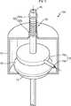
図1は、本発明の実施例によるDCバイアスを利用したリモートプラズマALD装置の概略的な図である。図1を参照するに、本発明の装置100は、大きく薄膜形成のための内部反応室10とプラズマを発生させるためのリモートプラズマ発生部30、リモートプラズマを調節するためのDCバイアス部50及びソースガス供給部70に分けられる。 FIG. 1 is a schematic diagram of a remote plasma ALD apparatus using a DC bias according to an embodiment of the present invention. Referring to FIG. 1, an
まず、本発明の装置100は、薄膜形成反応が起こる内部空間を有する反応室10を含む。反応室10の内部空間の一側には、基板支持台15が配置されており、この基板支持台15に薄膜形成のための基板16が載置される。基板16としては、シリコン(Si)基板を使用し、シリコンゲルマニウム(SiGe)、ゲルマニウム(Ge)、アルミニウム酸化物(Al2O3)、ガリウム砒素(GaAs)、シリコンカーバイド(SiC)基板を使用することもある。First, the
ソースガス供給部70は、反応室10の内部に薄膜形成のためのソースガスを供給する。基板16に成長させる薄膜物質は、シリコン酸化物のようなシリコン化合物であり、これに適したソースガスを供給する。ここで、ソースガス供給部70は、シャワーヘッド70aと、シャワーヘッド70aの一端に連結されてソースガスをシャワーヘッド70aに供給するソースガス供給管70bとより構成された例を図示した。このようにシャワーヘッドを利用する場合、従来のトラベリング方式に比べて基板の全面にわたって薄膜の均一性を確保しうる。しかし、ソースガス供給部70は、リングタイプまたはトラベリング方式でもよく、ここに言及されていない他の方式でも良い。また、当業者に公知されたように、1種類以上のソースガスを供給しなければならない必要がある場合を考慮して、一つ以上のソースガス供給管70bがシャワーヘッド70aに連結されうる。ほとんどの場合、特に、有機金属ソースガスの場合、色々な毒性を含有しうるので、シャワーヘッド70aの寿命を延長させるためには、ソースガスに対する反応抵抗性に優れる物質であるニッケルでシャワーヘッド70aを製作することが望ましい。 The source
本発明の装置100には、反応室10に連結されるキャリアガス供給部25も備えられるが、これは、ソースガスを反応室10の内部空間に流入させるためのキャリアガスの供給を担当する。そして、反応室10の外側にはキャリアガス供給部25と連通されるように、リモートプラズマ発生部30が設置されている。リモートプラズマ発生部30は、反応室10の内部空間にリモートプラズマを供給する。プラズマは、イオン化過程を通じて基板16に活性粒子を運搬して、塗布される薄膜物質の結合性を向上させ、かつ薄膜成長の均一性を増進させる。 The
図1のように、ソースガス供給部70をシャワーヘッドタイプで構成した場合、シャワーヘッド70aから噴射されるソースガスとリモートプラズマとを互いに分離された経路に基板16側に供給させるために、リモートプラズマもシャワーヘッドタイプで提供されるようにシャワーヘッド70aを構成することが望ましい。 As shown in FIG. 1, when the source
例えば、シャワーヘッド70aの概略的な縦断面の形態を示す図2を参照すれば、シャワーヘッド70aでソースガスの経路Sとリモートプラズマの経路Pとが分離されるように構成しうる。このためには、図3に示したように、シャワーヘッド70aの底面にソースガス供給管70bを通じて供給されたソースガスを反応室10の内部に噴射するために、所定直径の噴射ホール72を備えることに加えて、噴射ホール72と別途にリモートプラズマを供給するための貫通ホール74をさらに形成する。次いで、このようなシャワーヘッド70aをキャリアガス供給部25と連結されるように設置する。これにより、リモートプラズマ発生部30から発生したプラズマが経路Pを通じて基板16側に供給されうる。 For example, referring to FIG. 2 showing a schematic vertical cross-sectional form of the
再び、図1を参照して、キャリアガス供給部25にはリモートプラズマのエネルギーを調節しうるDCバイアス部50がさらに設置される。DCバイアス部50は、二つの対向電極50a,50bよりなり、第1電極50aが(+)である場合に第2電極50bが(−)となり、逆に、第1電極50aが(−)である場合に第2電極50bが(+)となる。対向電極50a,50bに加えられる電圧を調節してDCバイアスを調節することによって、窮極的にはプラズマ内の活性粒子フラックスを調節するようになる。したがって、ALD工程に適したプラズマの発生が可能になる。 Referring to FIG. 1 again, the carrier
このように、本発明装置100のDCバイアス部50を利用すれば、RFプラズマに発生するイオン及び電子のエネルギー調節が可能であり、プラズマの電子方向及び強度を調節しうる。したがって、ソースガスの適切なエネルギーを供給することによって原子層の薄膜蒸着に必要な単原子層の蒸着が可能になる。基板16に成長させる薄膜物質は、単結晶、多結晶または非晶質化合物でありうる。 As described above, by using the
このような装置100を利用して基板16上に薄膜を蒸着する方法は、次の通りである。 A method of depositing a thin film on the
反応室10内の基板支持台15上に基板16を載置した後、ソースガス供給部70を通じて反応室10の内部にソースガスを供給する。そして、キャリアガス供給部25を通じてキャリアガスも供給する。反応室10の外側に設置されたリモートプラズマ発生部30でリモートプラズマを発生させ、キャリアガス供給部25によって設置されたDCバイアス部50を通じてDCバイアスを利用し、リモートプラズマのエネルギーを調節する。これにより、プラズマのイオン、電子を捕獲または加速させる。このようにエネルギー調節されたところのリモートプラズマによってソースガスのラジカル生成を促進して基板16上に単原子層化合物の薄膜を成長させる。 After placing the
このように、本発明によるALD装置及び方法は、リモートプラズマを使用する。反応室10の外部に設置されたリモートプラズマ発生部30から発生して反応室の内部空間に流入されつつ、DCバイアス部50によってエネルギーが調節されたところのリモートプラズマは、従来のように反応室の内部で直接発生するプラズマに比べて基板と薄膜とに直接的な衝撃を与えない。したがって、プラズマによる基板及び薄膜の損傷を最小化させうる。そして、リモートプラズマで蒸着する時、反応炉の内部でのリモートプラズマの寿命の問題によってRFプラズマにDCバイアスを適用させて、RFプラズマの周波数領域帯である13.56MHzの影響を受けないリモートプラズマが反応炉の内部で前駆体と反応して安定したリモートプラズマの形成を期待できる。 Thus, the ALD apparatus and method according to the present invention uses remote plasma. The remote plasma whose energy is adjusted by the
以上、本発明の実施例について説明したが、本発明は前記実施例に限定されず、多様な変更や変形が可能である。本発明は特許請求の範囲によって定義される本発明の思想及び範囲内で決定されうる。 As mentioned above, although the Example of this invention was described, this invention is not limited to the said Example, A various change and deformation | transformation are possible. The invention may be determined within the spirit and scope of the invention as defined by the claims.
本発明の用途は下記の例に限定されるものではないが、このような本発明のDCバイアスを利用したリモートプラズマALD装置を利用してALD方法を行う一つの例として、リモートH2、N2、H2とN2との混合、O2、NH3プラズマと有機金属ソース、及びハロゲンソースを周期的に供給して金属、金属酸化物または金属窒化物を基板上に蒸着する方法が可能である。また、各種の化合物、すなわち、単結晶、非晶質、多結晶化合物を基板上に単原子層を蒸着するところに効果がある。Although the application of the present invention is not limited to the following example, as an example of performing the ALD method using the remote plasma ALD apparatus using the DC bias of the present invention, remote H2 , N2 , a mixture of H2 and N2 , O2 , NH3 plasma, organometallic source, and halogen source are periodically supplied to deposit metal, metal oxide or metal nitride on the substrate It is. Further, it is effective in depositing a monoatomic layer of various compounds, that is, single crystal, amorphous, and polycrystalline compounds on a substrate.
本発明のプラズマALD装置は、リモートプラズマを使用することが第1特徴であり、このようなプラズマの活性粒子フラックスをDCバイアスでもって調節することが第2特徴である。 The first feature of the plasma ALD apparatus of the present invention is the use of remote plasma, and the second feature is that the active particle flux of such plasma is adjusted with a DC bias.
反応室の外部に設置されたDCバイアスを利用したリモートプラズマ発生部から発生して反応室の内部空間に流入されるプラズマは、反応室の内部で直接発生するプラズマに比べて基板に直接的な衝撃を与えないので、プラズマによる基板及び薄膜の損傷を防止しうる。 The plasma generated from the remote plasma generator using a DC bias installed outside the reaction chamber and flowing into the reaction chamber internal space is more directly applied to the substrate than the plasma directly generated inside the reaction chamber. Since no impact is given, damage to the substrate and the thin film due to plasma can be prevented.
また、DCバイアスを利用してリモートプラズマのエネルギーを調節できて、ソースガスの適切なエネルギーを供給することによって、原子層の薄膜蒸着に必要な単原子層の蒸着が可能になる。 Further, the energy of the remote plasma can be adjusted using a DC bias, and by supplying an appropriate energy of the source gas, it is possible to deposit a monoatomic layer necessary for thin film deposition of an atomic layer.
Claims (20)
Translated fromJapanese前記反応室の内部空間の一側に配置され、薄膜形成のための基板が載置される基板支持台と、
前記反応室の外側に設置されて、前記反応室の内部空間にリモートプラズマを供給するためのリモートプラズマ発生部と、
前記反応室の外側に設けられ、前記リモートプラズマ発生部で発生したリモートプラズマのイオンと電子のエネルギーを調節しうるDCバイアス部と、
前記反応室の内部に薄膜形成のためのソースガスを供給するソースガス供給部と、を含むことを特徴とするDCバイアスを利用したリモートプラズマ原子層蒸着装置。A reaction chamber having an internal space;
A substrate support placed on one side of the internal space of the reaction chamber and on which a substrate for thin film formation is placed;
A remote plasma generator installed outside the reaction chamber for supplying remote plasma to the internal space of the reaction chamber;
A DC bias unitprovided outside the reaction chamber and capable of adjusting energyof ions and electrons of remote plasma generated by the remote plasma generation unit;
A remote plasma atomic layer deposition apparatus using a DC bias, comprising: a source gas supply unit configured to supply a source gas for forming a thin film into the reaction chamber.
前記反応室の内部空間の一側に配置され、薄膜形成のための基板が載置される基板支持台を供給する段階と、
ソースガス供給部から反応室の内部にソースガスを供給する段階と、
反応室の内部空間に流入されるキャリアガスを供給する段階と、
反応室の外側に設置されたリモートプラズマ発生部からリモートプラズマを発生させる段階と、
前記キャリアガス供給部に設置されたDCバイアス部に印加された電圧によってリモートプラズマエネルギーを調節する段階と、
DCバイアスを利用してプラズマのイオン、電子を捕獲または加速させる段階と、
リモートプラズマによってソースガスのラジカルの生成を促進して単原子層化合物薄膜を成長させる段階と、
前記基板上に単原子層化合物薄膜を蒸着する段階と、よりなるDCバイアスを利用したリモートプラズマ原子層蒸着方法。Providing a reaction chamber having an internal space;
Supplying a substrate support placed on one side of the internal space of the reaction chamber and on which a substrate for thin film formation is placed;
Supplying a source gas from the source gas supply unit into the reaction chamber;
Supplying a carrier gas flowing into the internal space of the reaction chamber;
Generating a remote plasma from a remote plasma generator installed outside the reaction chamber;
Adjusting remote plasma energy according to a voltage applied to a DC bias unit installed in the carrier gas supply unit;
Capturing or accelerating plasma ions and electrons using a DC bias;
Promoting the generation of source gas radicals by remote plasma to grow a monolayer compound thin film; and
A method of depositing a monoatomic layer compound thin film on the substrate, and a remote plasma atomic layer deposition method using a DC bias.
Applications Claiming Priority (1)
| Application Number | Priority Date | Filing Date | Title |
|---|---|---|---|
| PCT/KR2004/001962WO2006014034A1 (en) | 2004-08-04 | 2004-08-04 | Remote plasma atomic layer deposition apparatus and method using dc bias |
Publications (2)
| Publication Number | Publication Date |
|---|---|
| JP2008508430A JP2008508430A (en) | 2008-03-21 |
| JP4570659B2true JP4570659B2 (en) | 2010-10-27 |
Family
ID=35787303
Family Applications (1)
| Application Number | Title | Priority Date | Filing Date |
|---|---|---|---|
| JP2007524731AExpired - Fee RelatedJP4570659B2 (en) | 2004-08-04 | 2004-08-04 | Remote plasma atomic layer deposition apparatus and method using DC bias |
Country Status (4)
| Country | Link |
|---|---|
| US (1) | US20090011150A1 (en) |
| JP (1) | JP4570659B2 (en) |
| FI (1) | FI123594B (en) |
| WO (1) | WO2006014034A1 (en) |
Cited By (1)
| Publication number | Priority date | Publication date | Assignee | Title |
|---|---|---|---|---|
| US10286753B2 (en) | 2014-03-11 | 2019-05-14 | Mitsubishi Heavy Industries Thermal Systems, Ltd. | On-state malfunction detection device and method therefor |
Families Citing this family (286)
| Publication number | Priority date | Publication date | Assignee | Title |
|---|---|---|---|---|
| KR100505680B1 (en)* | 2003-03-27 | 2005-08-03 | 삼성전자주식회사 | Method for manufacturing semiconductor memory device having ruthenium film and apparatus for manufacturing the ruthenium film |
| US7842581B2 (en)* | 2003-03-27 | 2010-11-30 | Samsung Electronics Co., Ltd. | Methods of forming metal layers using oxygen gas as a reaction source and methods of fabricating capacitors using such metal layers |
| KR100956210B1 (en)* | 2007-06-19 | 2010-05-04 | 에어 프로덕츠 앤드 케미칼스, 인코오포레이티드 | Plasma Enhanced Cyclic Deposition of Metal Silicon Nitride Thin Films |
| US7964040B2 (en) | 2007-11-08 | 2011-06-21 | Applied Materials, Inc. | Multi-port pumping system for substrate processing chambers |
| US20120180954A1 (en) | 2011-01-18 | 2012-07-19 | Applied Materials, Inc. | Semiconductor processing system and methods using capacitively coupled plasma |
| US10225919B2 (en)* | 2011-06-30 | 2019-03-05 | Aes Global Holdings, Pte. Ltd | Projected plasma source |
| US20130023129A1 (en) | 2011-07-20 | 2013-01-24 | Asm America, Inc. | Pressure transmitter for a semiconductor processing environment |
| US8889566B2 (en) | 2012-09-11 | 2014-11-18 | Applied Materials, Inc. | Low cost flowable dielectric films |
| US10714315B2 (en) | 2012-10-12 | 2020-07-14 | Asm Ip Holdings B.V. | Semiconductor reaction chamber showerhead |
| US9018108B2 (en) | 2013-01-25 | 2015-04-28 | Applied Materials, Inc. | Low shrinkage dielectric films |
| US20160376700A1 (en) | 2013-02-01 | 2016-12-29 | Asm Ip Holding B.V. | System for treatment of deposition reactor |
| US20140273538A1 (en) | 2013-03-15 | 2014-09-18 | Tokyo Electron Limited | Non-ambipolar electric pressure plasma uniformity control |
| KR102109679B1 (en)* | 2013-11-07 | 2020-05-13 | 에이에스엠 아이피 홀딩 비.브이. | Method of depositing thin film |
| US11015245B2 (en) | 2014-03-19 | 2021-05-25 | Asm Ip Holding B.V. | Gas-phase reactor and system having exhaust plenum and components thereof |
| US9412581B2 (en) | 2014-07-16 | 2016-08-09 | Applied Materials, Inc. | Low-K dielectric gapfill by flowable deposition |
| CN104233227A (en)* | 2014-09-23 | 2014-12-24 | 上海华力微电子有限公司 | Atomic layer deposition equipment and method |
| US10941490B2 (en) | 2014-10-07 | 2021-03-09 | Asm Ip Holding B.V. | Multiple temperature range susceptor, assembly, reactor and system including the susceptor, and methods of using the same |
| KR101533032B1 (en)* | 2015-02-03 | 2015-07-01 | 성균관대학교산학협력단 | Thin film depositing apparatus |
| US10276355B2 (en) | 2015-03-12 | 2019-04-30 | Asm Ip Holding B.V. | Multi-zone reactor, system including the reactor, and method of using the same |
| US10458018B2 (en) | 2015-06-26 | 2019-10-29 | Asm Ip Holding B.V. | Structures including metal carbide material, devices including the structures, and methods of forming same |
| US10211308B2 (en) | 2015-10-21 | 2019-02-19 | Asm Ip Holding B.V. | NbMC layers |
| US11139308B2 (en) | 2015-12-29 | 2021-10-05 | Asm Ip Holding B.V. | Atomic layer deposition of III-V compounds to form V-NAND devices |
| US10529554B2 (en) | 2016-02-19 | 2020-01-07 | Asm Ip Holding B.V. | Method for forming silicon nitride film selectively on sidewalls or flat surfaces of trenches |
| US10343920B2 (en) | 2016-03-18 | 2019-07-09 | Asm Ip Holding B.V. | Aligned carbon nanotubes |
| US10367080B2 (en) | 2016-05-02 | 2019-07-30 | Asm Ip Holding B.V. | Method of forming a germanium oxynitride film |
| US11453943B2 (en) | 2016-05-25 | 2022-09-27 | Asm Ip Holding B.V. | Method for forming carbon-containing silicon/metal oxide or nitride film by ALD using silicon precursor and hydrocarbon precursor |
| US10612137B2 (en) | 2016-07-08 | 2020-04-07 | Asm Ip Holdings B.V. | Organic reactants for atomic layer deposition |
| US9859151B1 (en) | 2016-07-08 | 2018-01-02 | Asm Ip Holding B.V. | Selective film deposition method to form air gaps |
| US9887082B1 (en) | 2016-07-28 | 2018-02-06 | Asm Ip Holding B.V. | Method and apparatus for filling a gap |
| US9812320B1 (en) | 2016-07-28 | 2017-11-07 | Asm Ip Holding B.V. | Method and apparatus for filling a gap |
| KR102532607B1 (en) | 2016-07-28 | 2023-05-15 | 에이에스엠 아이피 홀딩 비.브이. | Substrate processing apparatus and method of operating the same |
| US11532757B2 (en) | 2016-10-27 | 2022-12-20 | Asm Ip Holding B.V. | Deposition of charge trapping layers |
| US10714350B2 (en) | 2016-11-01 | 2020-07-14 | ASM IP Holdings, B.V. | Methods for forming a transition metal niobium nitride film on a substrate by atomic layer deposition and related semiconductor device structures |
| KR102546317B1 (en) | 2016-11-15 | 2023-06-21 | 에이에스엠 아이피 홀딩 비.브이. | Gas supply unit and substrate processing apparatus including the same |
| KR102762543B1 (en) | 2016-12-14 | 2025-02-05 | 에이에스엠 아이피 홀딩 비.브이. | Substrate processing apparatus |
| US11447861B2 (en) | 2016-12-15 | 2022-09-20 | Asm Ip Holding B.V. | Sequential infiltration synthesis apparatus and a method of forming a patterned structure |
| US11581186B2 (en) | 2016-12-15 | 2023-02-14 | Asm Ip Holding B.V. | Sequential infiltration synthesis apparatus |
| KR102700194B1 (en) | 2016-12-19 | 2024-08-28 | 에이에스엠 아이피 홀딩 비.브이. | Substrate processing apparatus |
| US10269558B2 (en) | 2016-12-22 | 2019-04-23 | Asm Ip Holding B.V. | Method of forming a structure on a substrate |
| US11390950B2 (en) | 2017-01-10 | 2022-07-19 | Asm Ip Holding B.V. | Reactor system and method to reduce residue buildup during a film deposition process |
| US10468261B2 (en) | 2017-02-15 | 2019-11-05 | Asm Ip Holding B.V. | Methods for forming a metallic film on a substrate by cyclical deposition and related semiconductor device structures |
| US10529563B2 (en) | 2017-03-29 | 2020-01-07 | Asm Ip Holdings B.V. | Method for forming doped metal oxide films on a substrate by cyclical deposition and related semiconductor device structures |
| US10770286B2 (en) | 2017-05-08 | 2020-09-08 | Asm Ip Holdings B.V. | Methods for selectively forming a silicon nitride film on a substrate and related semiconductor device structures |
| US12040200B2 (en) | 2017-06-20 | 2024-07-16 | Asm Ip Holding B.V. | Semiconductor processing apparatus and methods for calibrating a semiconductor processing apparatus |
| US11306395B2 (en) | 2017-06-28 | 2022-04-19 | Asm Ip Holding B.V. | Methods for depositing a transition metal nitride film on a substrate by atomic layer deposition and related deposition apparatus |
| KR20190009245A (en) | 2017-07-18 | 2019-01-28 | 에이에스엠 아이피 홀딩 비.브이. | Methods for forming a semiconductor device structure and related semiconductor device structures |
| US11018002B2 (en) | 2017-07-19 | 2021-05-25 | Asm Ip Holding B.V. | Method for selectively depositing a Group IV semiconductor and related semiconductor device structures |
| US11374112B2 (en) | 2017-07-19 | 2022-06-28 | Asm Ip Holding B.V. | Method for depositing a group IV semiconductor and related semiconductor device structures |
| US10541333B2 (en) | 2017-07-19 | 2020-01-21 | Asm Ip Holding B.V. | Method for depositing a group IV semiconductor and related semiconductor device structures |
| US10590535B2 (en) | 2017-07-26 | 2020-03-17 | Asm Ip Holdings B.V. | Chemical treatment, deposition and/or infiltration apparatus and method for using the same |
| TWI815813B (en) | 2017-08-04 | 2023-09-21 | 荷蘭商Asm智慧財產控股公司 | Showerhead assembly for distributing a gas within a reaction chamber |
| US10770336B2 (en) | 2017-08-08 | 2020-09-08 | Asm Ip Holding B.V. | Substrate lift mechanism and reactor including same |
| US10692741B2 (en) | 2017-08-08 | 2020-06-23 | Asm Ip Holdings B.V. | Radiation shield |
| US11769682B2 (en) | 2017-08-09 | 2023-09-26 | Asm Ip Holding B.V. | Storage apparatus for storing cassettes for substrates and processing apparatus equipped therewith |
| US11139191B2 (en) | 2017-08-09 | 2021-10-05 | Asm Ip Holding B.V. | Storage apparatus for storing cassettes for substrates and processing apparatus equipped therewith |
| US11830730B2 (en) | 2017-08-29 | 2023-11-28 | Asm Ip Holding B.V. | Layer forming method and apparatus |
| KR102491945B1 (en) | 2017-08-30 | 2023-01-26 | 에이에스엠 아이피 홀딩 비.브이. | Substrate processing apparatus |
| US11295980B2 (en) | 2017-08-30 | 2022-04-05 | Asm Ip Holding B.V. | Methods for depositing a molybdenum metal film over a dielectric surface of a substrate by a cyclical deposition process and related semiconductor device structures |
| US11056344B2 (en) | 2017-08-30 | 2021-07-06 | Asm Ip Holding B.V. | Layer forming method |
| US10658205B2 (en) | 2017-09-28 | 2020-05-19 | Asm Ip Holdings B.V. | Chemical dispensing apparatus and methods for dispensing a chemical to a reaction chamber |
| US10403504B2 (en) | 2017-10-05 | 2019-09-03 | Asm Ip Holding B.V. | Method for selectively depositing a metallic film on a substrate |
| US10923344B2 (en) | 2017-10-30 | 2021-02-16 | Asm Ip Holding B.V. | Methods for forming a semiconductor structure and related semiconductor structures |
| US11022879B2 (en) | 2017-11-24 | 2021-06-01 | Asm Ip Holding B.V. | Method of forming an enhanced unexposed photoresist layer |
| WO2019103613A1 (en) | 2017-11-27 | 2019-05-31 | Asm Ip Holding B.V. | A storage device for storing wafer cassettes for use with a batch furnace |
| CN111344522B (en) | 2017-11-27 | 2022-04-12 | 阿斯莫Ip控股公司 | Including clean mini-environment device |
| US10872771B2 (en) | 2018-01-16 | 2020-12-22 | Asm Ip Holding B. V. | Method for depositing a material film on a substrate within a reaction chamber by a cyclical deposition process and related device structures |
| KR102695659B1 (en) | 2018-01-19 | 2024-08-14 | 에이에스엠 아이피 홀딩 비.브이. | Method for depositing a gap filling layer by plasma assisted deposition |
| TWI799494B (en) | 2018-01-19 | 2023-04-21 | 荷蘭商Asm 智慧財產控股公司 | Deposition method |
| US11081345B2 (en) | 2018-02-06 | 2021-08-03 | Asm Ip Holding B.V. | Method of post-deposition treatment for silicon oxide film |
| US10896820B2 (en) | 2018-02-14 | 2021-01-19 | Asm Ip Holding B.V. | Method for depositing a ruthenium-containing film on a substrate by a cyclical deposition process |
| WO2019158960A1 (en) | 2018-02-14 | 2019-08-22 | Asm Ip Holding B.V. | A method for depositing a ruthenium-containing film on a substrate by a cyclical deposition process |
| US10731249B2 (en) | 2018-02-15 | 2020-08-04 | Asm Ip Holding B.V. | Method of forming a transition metal containing film on a substrate by a cyclical deposition process, a method for supplying a transition metal halide compound to a reaction chamber, and related vapor deposition apparatus |
| KR102636427B1 (en) | 2018-02-20 | 2024-02-13 | 에이에스엠 아이피 홀딩 비.브이. | Substrate processing method and apparatus |
| US10975470B2 (en) | 2018-02-23 | 2021-04-13 | Asm Ip Holding B.V. | Apparatus for detecting or monitoring for a chemical precursor in a high temperature environment |
| US11473195B2 (en) | 2018-03-01 | 2022-10-18 | Asm Ip Holding B.V. | Semiconductor processing apparatus and a method for processing a substrate |
| US11629406B2 (en) | 2018-03-09 | 2023-04-18 | Asm Ip Holding B.V. | Semiconductor processing apparatus comprising one or more pyrometers for measuring a temperature of a substrate during transfer of the substrate |
| US11114283B2 (en) | 2018-03-16 | 2021-09-07 | Asm Ip Holding B.V. | Reactor, system including the reactor, and methods of manufacturing and using same |
| KR102646467B1 (en) | 2018-03-27 | 2024-03-11 | 에이에스엠 아이피 홀딩 비.브이. | Method of forming an electrode on a substrate and a semiconductor device structure including an electrode |
| US11230766B2 (en) | 2018-03-29 | 2022-01-25 | Asm Ip Holding B.V. | Substrate processing apparatus and method |
| US11088002B2 (en) | 2018-03-29 | 2021-08-10 | Asm Ip Holding B.V. | Substrate rack and a substrate processing system and method |
| KR102600229B1 (en) | 2018-04-09 | 2023-11-10 | 에이에스엠 아이피 홀딩 비.브이. | Substrate supporting device, substrate processing apparatus including the same and substrate processing method |
| US12025484B2 (en) | 2018-05-08 | 2024-07-02 | Asm Ip Holding B.V. | Thin film forming method |
| TWI811348B (en) | 2018-05-08 | 2023-08-11 | 荷蘭商Asm 智慧財產控股公司 | Methods for depositing an oxide film on a substrate by a cyclical deposition process and related device structures |
| US12272527B2 (en) | 2018-05-09 | 2025-04-08 | Asm Ip Holding B.V. | Apparatus for use with hydrogen radicals and method of using same |
| KR102596988B1 (en) | 2018-05-28 | 2023-10-31 | 에이에스엠 아이피 홀딩 비.브이. | Method of processing a substrate and a device manufactured by the same |
| TWI840362B (en) | 2018-06-04 | 2024-05-01 | 荷蘭商Asm Ip私人控股有限公司 | Wafer handling chamber with moisture reduction |
| US11718913B2 (en) | 2018-06-04 | 2023-08-08 | Asm Ip Holding B.V. | Gas distribution system and reactor system including same |
| US11286562B2 (en) | 2018-06-08 | 2022-03-29 | Asm Ip Holding B.V. | Gas-phase chemical reactor and method of using same |
| KR102568797B1 (en) | 2018-06-21 | 2023-08-21 | 에이에스엠 아이피 홀딩 비.브이. | Substrate processing system |
| US10797133B2 (en) | 2018-06-21 | 2020-10-06 | Asm Ip Holding B.V. | Method for depositing a phosphorus doped silicon arsenide film and related semiconductor device structures |
| KR102854019B1 (en) | 2018-06-27 | 2025-09-02 | 에이에스엠 아이피 홀딩 비.브이. | Periodic deposition method for forming a metal-containing material and films and structures comprising the metal-containing material |
| TWI873894B (en) | 2018-06-27 | 2025-02-21 | 荷蘭商Asm Ip私人控股有限公司 | Cyclic deposition methods for forming metal-containing material and films and structures including the metal-containing material |
| US10612136B2 (en) | 2018-06-29 | 2020-04-07 | ASM IP Holding, B.V. | Temperature-controlled flange and reactor system including same |
| US10388513B1 (en) | 2018-07-03 | 2019-08-20 | Asm Ip Holding B.V. | Method for depositing silicon-free carbon-containing film as gap-fill layer by pulse plasma-assisted deposition |
| US10755922B2 (en) | 2018-07-03 | 2020-08-25 | Asm Ip Holding B.V. | Method for depositing silicon-free carbon-containing film as gap-fill layer by pulse plasma-assisted deposition |
| WO2020027593A1 (en)* | 2018-08-01 | 2020-02-06 | 한양대학교 산학협력단 | Thin film deposition method using electron and ion controlling |
| US11053591B2 (en) | 2018-08-06 | 2021-07-06 | Asm Ip Holding B.V. | Multi-port gas injection system and reactor system including same |
| US11430674B2 (en) | 2018-08-22 | 2022-08-30 | Asm Ip Holding B.V. | Sensor array, apparatus for dispensing a vapor phase reactant to a reaction chamber and related methods |
| US11024523B2 (en) | 2018-09-11 | 2021-06-01 | Asm Ip Holding B.V. | Substrate processing apparatus and method |
| KR102707956B1 (en) | 2018-09-11 | 2024-09-19 | 에이에스엠 아이피 홀딩 비.브이. | Method for deposition of a thin film |
| US11049751B2 (en) | 2018-09-14 | 2021-06-29 | Asm Ip Holding B.V. | Cassette supply system to store and handle cassettes and processing apparatus equipped therewith |
| CN110970344B (en) | 2018-10-01 | 2024-10-25 | Asmip控股有限公司 | Substrate holding apparatus, system comprising the same and method of using the same |
| US11232963B2 (en) | 2018-10-03 | 2022-01-25 | Asm Ip Holding B.V. | Substrate processing apparatus and method |
| KR102592699B1 (en) | 2018-10-08 | 2023-10-23 | 에이에스엠 아이피 홀딩 비.브이. | Substrate support unit and apparatuses for depositing thin film and processing the substrate including the same |
| KR102605121B1 (en) | 2018-10-19 | 2023-11-23 | 에이에스엠 아이피 홀딩 비.브이. | Substrate processing apparatus and substrate processing method |
| KR102546322B1 (en) | 2018-10-19 | 2023-06-21 | 에이에스엠 아이피 홀딩 비.브이. | Substrate processing apparatus and substrate processing method |
| USD948463S1 (en) | 2018-10-24 | 2022-04-12 | Asm Ip Holding B.V. | Susceptor for semiconductor substrate supporting apparatus |
| US12378665B2 (en) | 2018-10-26 | 2025-08-05 | Asm Ip Holding B.V. | High temperature coatings for a preclean and etch apparatus and related methods |
| US11087997B2 (en) | 2018-10-31 | 2021-08-10 | Asm Ip Holding B.V. | Substrate processing apparatus for processing substrates |
| KR102748291B1 (en) | 2018-11-02 | 2024-12-31 | 에이에스엠 아이피 홀딩 비.브이. | Substrate support unit and substrate processing apparatus including the same |
| US11572620B2 (en) | 2018-11-06 | 2023-02-07 | Asm Ip Holding B.V. | Methods for selectively depositing an amorphous silicon film on a substrate |
| US11031242B2 (en) | 2018-11-07 | 2021-06-08 | Asm Ip Holding B.V. | Methods for depositing a boron doped silicon germanium film |
| US10818758B2 (en) | 2018-11-16 | 2020-10-27 | Asm Ip Holding B.V. | Methods for forming a metal silicate film on a substrate in a reaction chamber and related semiconductor device structures |
| US10847366B2 (en) | 2018-11-16 | 2020-11-24 | Asm Ip Holding B.V. | Methods for depositing a transition metal chalcogenide film on a substrate by a cyclical deposition process |
| US12040199B2 (en) | 2018-11-28 | 2024-07-16 | Asm Ip Holding B.V. | Substrate processing apparatus for processing substrates |
| US11217444B2 (en) | 2018-11-30 | 2022-01-04 | Asm Ip Holding B.V. | Method for forming an ultraviolet radiation responsive metal oxide-containing film |
| KR102636428B1 (en) | 2018-12-04 | 2024-02-13 | 에이에스엠 아이피 홀딩 비.브이. | A method for cleaning a substrate processing apparatus |
| US11158513B2 (en) | 2018-12-13 | 2021-10-26 | Asm Ip Holding B.V. | Methods for forming a rhenium-containing film on a substrate by a cyclical deposition process and related semiconductor device structures |
| TWI874340B (en) | 2018-12-14 | 2025-03-01 | 荷蘭商Asm Ip私人控股有限公司 | Method of forming device structure, structure formed by the method and system for performing the method |
| TWI866480B (en) | 2019-01-17 | 2024-12-11 | 荷蘭商Asm Ip 私人控股有限公司 | Methods of forming a transition metal containing film on a substrate by a cyclical deposition process |
| KR102727227B1 (en) | 2019-01-22 | 2024-11-07 | 에이에스엠 아이피 홀딩 비.브이. | Semiconductor processing device |
| CN111524788B (en) | 2019-02-01 | 2023-11-24 | Asm Ip私人控股有限公司 | Method for forming topologically selective films of silicon oxide |
| TWI873122B (en) | 2019-02-20 | 2025-02-21 | 荷蘭商Asm Ip私人控股有限公司 | Method of filling a recess formed within a surface of a substrate, semiconductor structure formed according to the method, and semiconductor processing apparatus |
| TWI845607B (en) | 2019-02-20 | 2024-06-21 | 荷蘭商Asm Ip私人控股有限公司 | Cyclical deposition method and apparatus for filling a recess formed within a substrate surface |
| TWI838458B (en) | 2019-02-20 | 2024-04-11 | 荷蘭商Asm Ip私人控股有限公司 | Apparatus and methods for plug fill deposition in 3-d nand applications |
| KR102626263B1 (en) | 2019-02-20 | 2024-01-16 | 에이에스엠 아이피 홀딩 비.브이. | Cyclical deposition method including treatment step and apparatus for same |
| TWI842826B (en) | 2019-02-22 | 2024-05-21 | 荷蘭商Asm Ip私人控股有限公司 | Substrate processing apparatus and method for processing substrate |
| KR102782593B1 (en) | 2019-03-08 | 2025-03-14 | 에이에스엠 아이피 홀딩 비.브이. | Structure Including SiOC Layer and Method of Forming Same |
| KR102858005B1 (en) | 2019-03-08 | 2025-09-09 | 에이에스엠 아이피 홀딩 비.브이. | Method for Selective Deposition of Silicon Nitride Layer and Structure Including Selectively-Deposited Silicon Nitride Layer |
| US11742198B2 (en) | 2019-03-08 | 2023-08-29 | Asm Ip Holding B.V. | Structure including SiOCN layer and method of forming same |
| JP2020167398A (en) | 2019-03-28 | 2020-10-08 | エーエスエム・アイピー・ホールディング・ベー・フェー | Door openers and substrate processing equipment provided with door openers |
| KR102809999B1 (en) | 2019-04-01 | 2025-05-19 | 에이에스엠 아이피 홀딩 비.브이. | Method of manufacturing semiconductor device |
| KR20200123380A (en) | 2019-04-19 | 2020-10-29 | 에이에스엠 아이피 홀딩 비.브이. | Layer forming method and apparatus |
| KR20200125453A (en) | 2019-04-24 | 2020-11-04 | 에이에스엠 아이피 홀딩 비.브이. | Gas-phase reactor system and method of using same |
| US11289326B2 (en) | 2019-05-07 | 2022-03-29 | Asm Ip Holding B.V. | Method for reforming amorphous carbon polymer film |
| KR20200130121A (en) | 2019-05-07 | 2020-11-18 | 에이에스엠 아이피 홀딩 비.브이. | Chemical source vessel with dip tube |
| KR20200130652A (en) | 2019-05-10 | 2020-11-19 | 에이에스엠 아이피 홀딩 비.브이. | Method of depositing material onto a surface and structure formed according to the method |
| JP7598201B2 (en) | 2019-05-16 | 2024-12-11 | エーエスエム・アイピー・ホールディング・ベー・フェー | Wafer boat handling apparatus, vertical batch furnace and method |
| JP7612342B2 (en) | 2019-05-16 | 2025-01-14 | エーエスエム・アイピー・ホールディング・ベー・フェー | Wafer boat handling apparatus, vertical batch furnace and method |
| USD947913S1 (en) | 2019-05-17 | 2022-04-05 | Asm Ip Holding B.V. | Susceptor shaft |
| USD975665S1 (en) | 2019-05-17 | 2023-01-17 | Asm Ip Holding B.V. | Susceptor shaft |
| USD935572S1 (en) | 2019-05-24 | 2021-11-09 | Asm Ip Holding B.V. | Gas channel plate |
| USD922229S1 (en) | 2019-06-05 | 2021-06-15 | Asm Ip Holding B.V. | Device for controlling a temperature of a gas supply unit |
| KR20200141002A (en) | 2019-06-06 | 2020-12-17 | 에이에스엠 아이피 홀딩 비.브이. | Method of using a gas-phase reactor system including analyzing exhausted gas |
| KR20200141931A (en) | 2019-06-10 | 2020-12-21 | 에이에스엠 아이피 홀딩 비.브이. | Method for cleaning quartz epitaxial chambers |
| KR20200143254A (en) | 2019-06-11 | 2020-12-23 | 에이에스엠 아이피 홀딩 비.브이. | Method of forming an electronic structure using an reforming gas, system for performing the method, and structure formed using the method |
| USD944946S1 (en) | 2019-06-14 | 2022-03-01 | Asm Ip Holding B.V. | Shower plate |
| USD931978S1 (en) | 2019-06-27 | 2021-09-28 | Asm Ip Holding B.V. | Showerhead vacuum transport |
| KR20210005515A (en) | 2019-07-03 | 2021-01-14 | 에이에스엠 아이피 홀딩 비.브이. | Temperature control assembly for substrate processing apparatus and method of using same |
| JP7499079B2 (en) | 2019-07-09 | 2024-06-13 | エーエスエム・アイピー・ホールディング・ベー・フェー | Plasma device using coaxial waveguide and substrate processing method |
| CN112216646A (en) | 2019-07-10 | 2021-01-12 | Asm Ip私人控股有限公司 | Substrate supporting assembly and substrate processing device comprising same |
| KR20210010307A (en) | 2019-07-16 | 2021-01-27 | 에이에스엠 아이피 홀딩 비.브이. | Substrate processing apparatus |
| KR102860110B1 (en) | 2019-07-17 | 2025-09-16 | 에이에스엠 아이피 홀딩 비.브이. | Methods of forming silicon germanium structures |
| KR20210010816A (en) | 2019-07-17 | 2021-01-28 | 에이에스엠 아이피 홀딩 비.브이. | Radical assist ignition plasma system and method |
| US11643724B2 (en) | 2019-07-18 | 2023-05-09 | Asm Ip Holding B.V. | Method of forming structures using a neutral beam |
| KR20210010817A (en) | 2019-07-19 | 2021-01-28 | 에이에스엠 아이피 홀딩 비.브이. | Method of Forming Topology-Controlled Amorphous Carbon Polymer Film |
| TWI839544B (en) | 2019-07-19 | 2024-04-21 | 荷蘭商Asm Ip私人控股有限公司 | Method of forming topology-controlled amorphous carbon polymer film |
| TWI851767B (en) | 2019-07-29 | 2024-08-11 | 荷蘭商Asm Ip私人控股有限公司 | Methods for selective deposition utilizing n-type dopants and/or alternative dopants to achieve high dopant incorporation |
| CN112309900A (en) | 2019-07-30 | 2021-02-02 | Asm Ip私人控股有限公司 | Substrate processing apparatus |
| US12169361B2 (en) | 2019-07-30 | 2024-12-17 | Asm Ip Holding B.V. | Substrate processing apparatus and method |
| CN112309899A (en) | 2019-07-30 | 2021-02-02 | Asm Ip私人控股有限公司 | Substrate processing apparatus |
| US11587814B2 (en) | 2019-07-31 | 2023-02-21 | Asm Ip Holding B.V. | Vertical batch furnace assembly |
| US11227782B2 (en) | 2019-07-31 | 2022-01-18 | Asm Ip Holding B.V. | Vertical batch furnace assembly |
| US11587815B2 (en) | 2019-07-31 | 2023-02-21 | Asm Ip Holding B.V. | Vertical batch furnace assembly |
| CN112323048B (en) | 2019-08-05 | 2024-02-09 | Asm Ip私人控股有限公司 | Liquid level sensor for chemical source container |
| CN112342526A (en) | 2019-08-09 | 2021-02-09 | Asm Ip私人控股有限公司 | Heater assembly including cooling device and method of using same |
| USD965524S1 (en) | 2019-08-19 | 2022-10-04 | Asm Ip Holding B.V. | Susceptor support |
| USD965044S1 (en) | 2019-08-19 | 2022-09-27 | Asm Ip Holding B.V. | Susceptor shaft |
| JP2021031769A (en) | 2019-08-21 | 2021-03-01 | エーエスエム アイピー ホールディング ビー.ブイ. | Production apparatus of mixed gas of film deposition raw material and film deposition apparatus |
| KR20210024423A (en) | 2019-08-22 | 2021-03-05 | 에이에스엠 아이피 홀딩 비.브이. | Method for forming a structure with a hole |
| USD930782S1 (en) | 2019-08-22 | 2021-09-14 | Asm Ip Holding B.V. | Gas distributor |
| USD979506S1 (en) | 2019-08-22 | 2023-02-28 | Asm Ip Holding B.V. | Insulator |
| USD949319S1 (en) | 2019-08-22 | 2022-04-19 | Asm Ip Holding B.V. | Exhaust duct |
| USD940837S1 (en) | 2019-08-22 | 2022-01-11 | Asm Ip Holding B.V. | Electrode |
| US11286558B2 (en) | 2019-08-23 | 2022-03-29 | Asm Ip Holding B.V. | Methods for depositing a molybdenum nitride film on a surface of a substrate by a cyclical deposition process and related semiconductor device structures including a molybdenum nitride film |
| KR20210024420A (en) | 2019-08-23 | 2021-03-05 | 에이에스엠 아이피 홀딩 비.브이. | Method for depositing silicon oxide film having improved quality by peald using bis(diethylamino)silane |
| KR102806450B1 (en) | 2019-09-04 | 2025-05-12 | 에이에스엠 아이피 홀딩 비.브이. | Methods for selective deposition using a sacrificial capping layer |
| KR102733104B1 (en) | 2019-09-05 | 2024-11-22 | 에이에스엠 아이피 홀딩 비.브이. | Substrate processing apparatus |
| US11562901B2 (en) | 2019-09-25 | 2023-01-24 | Asm Ip Holding B.V. | Substrate processing method |
| CN112593212B (en) | 2019-10-02 | 2023-12-22 | Asm Ip私人控股有限公司 | Method for forming topologically selective silicon oxide film by cyclic plasma enhanced deposition process |
| TW202128273A (en) | 2019-10-08 | 2021-08-01 | 荷蘭商Asm Ip私人控股有限公司 | Gas injection system, reactor system, and method of depositing material on surface of substratewithin reaction chamber |
| KR20210042810A (en) | 2019-10-08 | 2021-04-20 | 에이에스엠 아이피 홀딩 비.브이. | Reactor system including a gas distribution assembly for use with activated species and method of using same |
| TWI846953B (en) | 2019-10-08 | 2024-07-01 | 荷蘭商Asm Ip私人控股有限公司 | Substrate processing device |
| TWI846966B (en) | 2019-10-10 | 2024-07-01 | 荷蘭商Asm Ip私人控股有限公司 | Method of forming a photoresist underlayer and structure including same |
| US12009241B2 (en) | 2019-10-14 | 2024-06-11 | Asm Ip Holding B.V. | Vertical batch furnace assembly with detector to detect cassette |
| TWI834919B (en) | 2019-10-16 | 2024-03-11 | 荷蘭商Asm Ip私人控股有限公司 | Method of topology-selective film formation of silicon oxide |
| US11637014B2 (en) | 2019-10-17 | 2023-04-25 | Asm Ip Holding B.V. | Methods for selective deposition of doped semiconductor material |
| KR102845724B1 (en) | 2019-10-21 | 2025-08-13 | 에이에스엠 아이피 홀딩 비.브이. | Apparatus and methods for selectively etching films |
| KR20210050453A (en) | 2019-10-25 | 2021-05-07 | 에이에스엠 아이피 홀딩 비.브이. | Methods for filling a gap feature on a substrate surface and related semiconductor structures |
| US11646205B2 (en) | 2019-10-29 | 2023-05-09 | Asm Ip Holding B.V. | Methods of selectively forming n-type doped material on a surface, systems for selectively forming n-type doped material, and structures formed using same |
| KR20210054983A (en) | 2019-11-05 | 2021-05-14 | 에이에스엠 아이피 홀딩 비.브이. | Structures with doped semiconductor layers and methods and systems for forming same |
| US11501968B2 (en) | 2019-11-15 | 2022-11-15 | Asm Ip Holding B.V. | Method for providing a semiconductor device with silicon filled gaps |
| KR102861314B1 (en) | 2019-11-20 | 2025-09-17 | 에이에스엠 아이피 홀딩 비.브이. | Method of depositing carbon-containing material on a surface of a substrate, structure formed using the method, and system for forming the structure |
| US11450529B2 (en) | 2019-11-26 | 2022-09-20 | Asm Ip Holding B.V. | Methods for selectively forming a target film on a substrate comprising a first dielectric surface and a second metallic surface |
| CN112951697B (en) | 2019-11-26 | 2025-07-29 | Asmip私人控股有限公司 | Substrate processing apparatus |
| CN112885692B (en) | 2019-11-29 | 2025-08-15 | Asmip私人控股有限公司 | Substrate processing apparatus |
| CN120432376A (en) | 2019-11-29 | 2025-08-05 | Asm Ip私人控股有限公司 | Substrate processing apparatus |
| JP7527928B2 (en) | 2019-12-02 | 2024-08-05 | エーエスエム・アイピー・ホールディング・ベー・フェー | Substrate processing apparatus and substrate processing method |
| KR20210070898A (en) | 2019-12-04 | 2021-06-15 | 에이에스엠 아이피 홀딩 비.브이. | Substrate processing apparatus |
| KR20210078405A (en) | 2019-12-17 | 2021-06-28 | 에이에스엠 아이피 홀딩 비.브이. | Method of forming vanadium nitride layer and structure including the vanadium nitride layer |
| KR20210080214A (en) | 2019-12-19 | 2021-06-30 | 에이에스엠 아이피 홀딩 비.브이. | Methods for filling a gap feature on a substrate and related semiconductor structures |
| JP7730637B2 (en) | 2020-01-06 | 2025-08-28 | エーエスエム・アイピー・ホールディング・ベー・フェー | Gas delivery assembly, components thereof, and reactor system including same |
| JP7636892B2 (en) | 2020-01-06 | 2025-02-27 | エーエスエム・アイピー・ホールディング・ベー・フェー | Channeled Lift Pins |
| US11993847B2 (en) | 2020-01-08 | 2024-05-28 | Asm Ip Holding B.V. | Injector |
| KR20210093163A (en) | 2020-01-16 | 2021-07-27 | 에이에스엠 아이피 홀딩 비.브이. | Method of forming high aspect ratio features |
| KR102675856B1 (en) | 2020-01-20 | 2024-06-17 | 에이에스엠 아이피 홀딩 비.브이. | Method of forming thin film and method of modifying surface of thin film |
| TWI889744B (en) | 2020-01-29 | 2025-07-11 | 荷蘭商Asm Ip私人控股有限公司 | Contaminant trap system, and baffle plate stack |
| TW202513845A (en) | 2020-02-03 | 2025-04-01 | 荷蘭商Asm Ip私人控股有限公司 | Semiconductor structures and methods for forming the same |
| KR20210100010A (en) | 2020-02-04 | 2021-08-13 | 에이에스엠 아이피 홀딩 비.브이. | Method and apparatus for transmittance measurements of large articles |
| US11776846B2 (en) | 2020-02-07 | 2023-10-03 | Asm Ip Holding B.V. | Methods for depositing gap filling fluids and related systems and devices |
| TW202146691A (en) | 2020-02-13 | 2021-12-16 | 荷蘭商Asm Ip私人控股有限公司 | Gas distribution assembly, shower plate assembly, and method of adjusting conductance of gas to reaction chamber |
| KR20210103956A (en) | 2020-02-13 | 2021-08-24 | 에이에스엠 아이피 홀딩 비.브이. | Substrate processing apparatus including light receiving device and calibration method of light receiving device |
| TWI855223B (en) | 2020-02-17 | 2024-09-11 | 荷蘭商Asm Ip私人控股有限公司 | Method for growing phosphorous-doped silicon layer |
| CN113410160A (en) | 2020-02-28 | 2021-09-17 | Asm Ip私人控股有限公司 | System specially used for cleaning parts |
| KR20210113043A (en) | 2020-03-04 | 2021-09-15 | 에이에스엠 아이피 홀딩 비.브이. | Alignment fixture for a reactor system |
| US11876356B2 (en) | 2020-03-11 | 2024-01-16 | Asm Ip Holding B.V. | Lockout tagout assembly and system and method of using same |
| KR20210116240A (en) | 2020-03-11 | 2021-09-27 | 에이에스엠 아이피 홀딩 비.브이. | Substrate handling device with adjustable joints |
| KR102775390B1 (en) | 2020-03-12 | 2025-02-28 | 에이에스엠 아이피 홀딩 비.브이. | Method for Fabricating Layer Structure Having Target Topological Profile |
| US12173404B2 (en) | 2020-03-17 | 2024-12-24 | Asm Ip Holding B.V. | Method of depositing epitaxial material, structure formed using the method, and system for performing the method |
| KR102755229B1 (en) | 2020-04-02 | 2025-01-14 | 에이에스엠 아이피 홀딩 비.브이. | Thin film forming method |
| TWI887376B (en) | 2020-04-03 | 2025-06-21 | 荷蘭商Asm Ip私人控股有限公司 | Method for manufacturing semiconductor device |
| TWI888525B (en) | 2020-04-08 | 2025-07-01 | 荷蘭商Asm Ip私人控股有限公司 | Apparatus and methods for selectively etching silcon oxide films |
| KR20210128343A (en) | 2020-04-15 | 2021-10-26 | 에이에스엠 아이피 홀딩 비.브이. | Method of forming chromium nitride layer and structure including the chromium nitride layer |
| US11821078B2 (en) | 2020-04-15 | 2023-11-21 | Asm Ip Holding B.V. | Method for forming precoat film and method for forming silicon-containing film |
| US11996289B2 (en) | 2020-04-16 | 2024-05-28 | Asm Ip Holding B.V. | Methods of forming structures including silicon germanium and silicon layers, devices formed using the methods, and systems for performing the methods |
| KR20210130646A (en) | 2020-04-21 | 2021-11-01 | 에이에스엠 아이피 홀딩 비.브이. | Method for processing a substrate |
| TW202208671A (en) | 2020-04-24 | 2022-03-01 | 荷蘭商Asm Ip私人控股有限公司 | Methods of forming structures including vanadium boride and vanadium phosphide layers |
| KR20210132600A (en) | 2020-04-24 | 2021-11-04 | 에이에스엠 아이피 홀딩 비.브이. | Methods and systems for depositing a layer comprising vanadium, nitrogen, and a further element |
| KR20210132612A (en) | 2020-04-24 | 2021-11-04 | 에이에스엠 아이피 홀딩 비.브이. | Methods and apparatus for stabilizing vanadium compounds |
| CN113555279A (en) | 2020-04-24 | 2021-10-26 | Asm Ip私人控股有限公司 | Methods of forming vanadium nitride-containing layers and structures comprising the same |
| KR102866804B1 (en) | 2020-04-24 | 2025-09-30 | 에이에스엠 아이피 홀딩 비.브이. | Vertical batch furnace assembly comprising a cooling gas supply |
| KR102783898B1 (en) | 2020-04-29 | 2025-03-18 | 에이에스엠 아이피 홀딩 비.브이. | Solid source precursor vessel |
| KR20210134869A (en) | 2020-05-01 | 2021-11-11 | 에이에스엠 아이피 홀딩 비.브이. | Fast FOUP swapping with a FOUP handler |
| JP7726664B2 (en) | 2020-05-04 | 2025-08-20 | エーエスエム・アイピー・ホールディング・ベー・フェー | Substrate processing system for processing a substrate |
| KR102788543B1 (en) | 2020-05-13 | 2025-03-27 | 에이에스엠 아이피 홀딩 비.브이. | Laser alignment fixture for a reactor system |
| TW202146699A (en) | 2020-05-15 | 2021-12-16 | 荷蘭商Asm Ip私人控股有限公司 | Method of forming a silicon germanium layer, semiconductor structure, semiconductor device, method of forming a deposition layer, and deposition system |
| KR20210143653A (en) | 2020-05-19 | 2021-11-29 | 에이에스엠 아이피 홀딩 비.브이. | Substrate processing apparatus |
| KR102795476B1 (en) | 2020-05-21 | 2025-04-11 | 에이에스엠 아이피 홀딩 비.브이. | Structures including multiple carbon layers and methods of forming and using same |
| KR20210145079A (en) | 2020-05-21 | 2021-12-01 | 에이에스엠 아이피 홀딩 비.브이. | Flange and apparatus for processing substrates |
| TWI873343B (en) | 2020-05-22 | 2025-02-21 | 荷蘭商Asm Ip私人控股有限公司 | Reaction system for forming thin film on substrate |
| KR20210146802A (en) | 2020-05-26 | 2021-12-06 | 에이에스엠 아이피 홀딩 비.브이. | Method for depositing boron and gallium containing silicon germanium layers |
| TWI876048B (en) | 2020-05-29 | 2025-03-11 | 荷蘭商Asm Ip私人控股有限公司 | Substrate processing device |
| TW202212620A (en) | 2020-06-02 | 2022-04-01 | 荷蘭商Asm Ip私人控股有限公司 | Apparatus for processing substrate, method of forming film, and method of controlling apparatus for processing substrate |
| TW202208659A (en) | 2020-06-16 | 2022-03-01 | 荷蘭商Asm Ip私人控股有限公司 | Method for depositing boron containing silicon germanium layers |
| TW202218133A (en) | 2020-06-24 | 2022-05-01 | 荷蘭商Asm Ip私人控股有限公司 | Method for forming a layer provided with silicon |
| TWI873359B (en) | 2020-06-30 | 2025-02-21 | 荷蘭商Asm Ip私人控股有限公司 | Substrate processing method |
| US12431354B2 (en) | 2020-07-01 | 2025-09-30 | Asm Ip Holding B.V. | Silicon nitride and silicon oxide deposition methods using fluorine inhibitor |
| TW202202649A (en) | 2020-07-08 | 2022-01-16 | 荷蘭商Asm Ip私人控股有限公司 | Substrate processing method |
| KR20220010438A (en) | 2020-07-17 | 2022-01-25 | 에이에스엠 아이피 홀딩 비.브이. | Structures and methods for use in photolithography |
| KR20220011092A (en) | 2020-07-20 | 2022-01-27 | 에이에스엠 아이피 홀딩 비.브이. | Method and system for forming structures including transition metal layers |
| TWI878570B (en) | 2020-07-20 | 2025-04-01 | 荷蘭商Asm Ip私人控股有限公司 | Method and system for depositing molybdenum layers |
| US12322591B2 (en) | 2020-07-27 | 2025-06-03 | Asm Ip Holding B.V. | Thin film deposition process |
| KR20220021863A (en) | 2020-08-14 | 2022-02-22 | 에이에스엠 아이피 홀딩 비.브이. | Method for processing a substrate |
| US12040177B2 (en) | 2020-08-18 | 2024-07-16 | Asm Ip Holding B.V. | Methods for forming a laminate film by cyclical plasma-enhanced deposition processes |
| TW202228863A (en) | 2020-08-25 | 2022-08-01 | 荷蘭商Asm Ip私人控股有限公司 | Method for cleaning a substrate, method for selectively depositing, and reaction system |
| US11725280B2 (en) | 2020-08-26 | 2023-08-15 | Asm Ip Holding B.V. | Method for forming metal silicon oxide and metal silicon oxynitride layers |
| TW202229601A (en) | 2020-08-27 | 2022-08-01 | 荷蘭商Asm Ip私人控股有限公司 | Method of forming patterned structures, method of manipulating mechanical property, device structure, and substrate processing system |
| TW202217045A (en) | 2020-09-10 | 2022-05-01 | 荷蘭商Asm Ip私人控股有限公司 | Methods for depositing gap filing fluids and related systems and devices |
| USD990534S1 (en) | 2020-09-11 | 2023-06-27 | Asm Ip Holding B.V. | Weighted lift pin |
| KR20220036866A (en) | 2020-09-16 | 2022-03-23 | 에이에스엠 아이피 홀딩 비.브이. | Silicon oxide deposition method |
| USD1012873S1 (en) | 2020-09-24 | 2024-01-30 | Asm Ip Holding B.V. | Electrode for semiconductor processing apparatus |
| TWI889903B (en) | 2020-09-25 | 2025-07-11 | 荷蘭商Asm Ip私人控股有限公司 | Semiconductor processing method |
| US12009224B2 (en) | 2020-09-29 | 2024-06-11 | Asm Ip Holding B.V. | Apparatus and method for etching metal nitrides |
| KR20220045900A (en) | 2020-10-06 | 2022-04-13 | 에이에스엠 아이피 홀딩 비.브이. | Deposition method and an apparatus for depositing a silicon-containing material |
| CN114293174A (en) | 2020-10-07 | 2022-04-08 | Asm Ip私人控股有限公司 | Gas supply unit and substrate processing apparatus including the same |
| TW202229613A (en) | 2020-10-14 | 2022-08-01 | 荷蘭商Asm Ip私人控股有限公司 | Method of depositing material on stepped structure |
| TW202232565A (en) | 2020-10-15 | 2022-08-16 | 荷蘭商Asm Ip私人控股有限公司 | Method of manufacturing semiconductor device, and substrate treatment apparatus using ether-cat |
| TW202217037A (en) | 2020-10-22 | 2022-05-01 | 荷蘭商Asm Ip私人控股有限公司 | Method of depositing vanadium metal, structure, device and a deposition assembly |
| TW202223136A (en) | 2020-10-28 | 2022-06-16 | 荷蘭商Asm Ip私人控股有限公司 | Method for forming layer on substrate, and semiconductor processing system |
| TW202229620A (en) | 2020-11-12 | 2022-08-01 | 特文特大學 | Deposition system, method for controlling reaction condition, method for depositing |
| TW202229795A (en) | 2020-11-23 | 2022-08-01 | 荷蘭商Asm Ip私人控股有限公司 | A substrate processing apparatus with an injector |
| TW202235649A (en) | 2020-11-24 | 2022-09-16 | 荷蘭商Asm Ip私人控股有限公司 | Methods for filling a gap and related systems and devices |
| TW202235675A (en) | 2020-11-30 | 2022-09-16 | 荷蘭商Asm Ip私人控股有限公司 | Injector, and substrate processing apparatus |
| US12255053B2 (en) | 2020-12-10 | 2025-03-18 | Asm Ip Holding B.V. | Methods and systems for depositing a layer |
| TW202233884A (en) | 2020-12-14 | 2022-09-01 | 荷蘭商Asm Ip私人控股有限公司 | Method of forming structures for threshold voltage control |
| US11946137B2 (en) | 2020-12-16 | 2024-04-02 | Asm Ip Holding B.V. | Runout and wobble measurement fixtures |
| TW202232639A (en) | 2020-12-18 | 2022-08-16 | 荷蘭商Asm Ip私人控股有限公司 | Wafer processing apparatus with a rotatable table |
| TW202231903A (en) | 2020-12-22 | 2022-08-16 | 荷蘭商Asm Ip私人控股有限公司 | Transition metal deposition method, transition metal layer, and deposition assembly for depositing transition metal on substrate |
| TW202242184A (en) | 2020-12-22 | 2022-11-01 | 荷蘭商Asm Ip私人控股有限公司 | Precursor capsule, precursor vessel, vapor deposition assembly, and method of loading solid precursor into precursor vessel |
| TW202226899A (en) | 2020-12-22 | 2022-07-01 | 荷蘭商Asm Ip私人控股有限公司 | Plasma treatment device having matching box |
| USD1023959S1 (en) | 2021-05-11 | 2024-04-23 | Asm Ip Holding B.V. | Electrode for substrate processing apparatus |
| USD980814S1 (en) | 2021-05-11 | 2023-03-14 | Asm Ip Holding B.V. | Gas distributor for substrate processing apparatus |
| USD981973S1 (en) | 2021-05-11 | 2023-03-28 | Asm Ip Holding B.V. | Reactor wall for substrate processing apparatus |
| USD980813S1 (en) | 2021-05-11 | 2023-03-14 | Asm Ip Holding B.V. | Gas flow control plate for substrate processing apparatus |
| USD990441S1 (en) | 2021-09-07 | 2023-06-27 | Asm Ip Holding B.V. | Gas flow control plate |
| USD1060598S1 (en) | 2021-12-03 | 2025-02-04 | Asm Ip Holding B.V. | Split showerhead cover |
Family Cites Families (16)
| Publication number | Priority date | Publication date | Assignee | Title |
|---|---|---|---|---|
| JPH02240293A (en)* | 1989-03-14 | 1990-09-25 | Canon Inc | Production of anodically oxidized film |
| JP2888258B2 (en)* | 1990-11-30 | 1999-05-10 | 東京エレクトロン株式会社 | Substrate processing apparatus and substrate processing method |
| JPH09316647A (en)* | 1996-05-24 | 1997-12-09 | Suzuki Motor Corp | Thin film forming device by plasma cvd |
| JPH10107010A (en)* | 1996-09-30 | 1998-04-24 | Matsushita Electric Works Ltd | Dry etching apparatus of semiconductor device and dry etching thereof |
| US6152070A (en)* | 1996-11-18 | 2000-11-28 | Applied Materials, Inc. | Tandem process chamber |
| US6312554B1 (en)* | 1996-12-05 | 2001-11-06 | Applied Materials, Inc. | Apparatus and method for controlling the ratio of reactive to non-reactive ions in a semiconductor wafer processing chamber |
| JP4151862B2 (en)* | 1998-02-26 | 2008-09-17 | キヤノンアネルバ株式会社 | CVD equipment |
| US6182603B1 (en)* | 1998-07-13 | 2001-02-06 | Applied Komatsu Technology, Inc. | Surface-treated shower head for use in a substrate processing chamber |
| KR100704591B1 (en)* | 2000-03-21 | 2007-04-09 | 주성엔지니어링(주) | CD device and internal cleaning method |
| JP4371543B2 (en)* | 2000-06-29 | 2009-11-25 | 日本電気株式会社 | Remote plasma CVD apparatus and film forming method |
| US6391803B1 (en)* | 2001-06-20 | 2002-05-21 | Samsung Electronics Co., Ltd. | Method of forming silicon containing thin films by atomic layer deposition utilizing trisdimethylaminosilane |
| AU2002366943A1 (en)* | 2001-12-20 | 2003-07-09 | Tokyo Electron Limited | Method and apparatus comprising a magnetic filter for plasma processing a workpiece |
| AU2003238853A1 (en)* | 2002-01-25 | 2003-09-02 | Applied Materials, Inc. | Apparatus for cyclical deposition of thin films |
| KR100488426B1 (en)* | 2002-09-09 | 2005-05-11 | 주식회사 다산 씨.앤드.아이 | Remote plasma atomic layer chemical vapor deposition apparatus and method |
| US20060035470A1 (en)* | 2002-10-30 | 2006-02-16 | Hitachi Kokusai Electronic, Inc. | Method for manufaturing semiconductor device and substrate processing system |
| KR100529298B1 (en)* | 2003-03-20 | 2005-11-17 | 학교법인 한양학원 | Remote plasma atomic layer deposition apparatus using DC bias |
- 2004
- 2004-08-04JPJP2007524731Apatent/JP4570659B2/ennot_activeExpired - Fee Related
- 2004-08-04USUS11/658,961patent/US20090011150A1/ennot_activeAbandoned
- 2004-08-04WOPCT/KR2004/001962patent/WO2006014034A1/enactiveApplication Filing
- 2007
- 2007-02-21FIFI20075125Apatent/FI123594B/ennot_activeIP Right Cessation
Cited By (1)
| Publication number | Priority date | Publication date | Assignee | Title |
|---|---|---|---|---|
| US10286753B2 (en) | 2014-03-11 | 2019-05-14 | Mitsubishi Heavy Industries Thermal Systems, Ltd. | On-state malfunction detection device and method therefor |
Also Published As
| Publication number | Publication date |
|---|---|
| JP2008508430A (en) | 2008-03-21 |
| FI20075125L (en) | 2007-02-21 |
| WO2006014034A1 (en) | 2006-02-09 |
| US20090011150A1 (en) | 2009-01-08 |
| FI123594B (en) | 2013-07-31 |
Similar Documents
| Publication | Publication Date | Title |
|---|---|---|
| JP4570659B2 (en) | Remote plasma atomic layer deposition apparatus and method using DC bias | |
| AU2010212553B2 (en) | Migration and plasma enhanced chemical vapor deposition | |
| JP5214251B2 (en) | Equipment for high density low energy plasma vapor phase epitaxy. | |
| JP2021123800A (en) | A method of forming a structure containing a carbon material, a structure formed using the method, and a system for forming the structure. | |
| WO2000044033A1 (en) | Method and apparatus for film deposition | |
| WO2000063956A1 (en) | Method and apparatus for thin-film deposition, and method of manufacturing thin-film semiconductor device | |
| CN102007597A (en) | Low temperature thin film transistor process, device property, and device stability improvement | |
| JP2010520638A (en) | Atomic layer deposition technology | |
| CN103572248A (en) | Diamond producing method and DC plasma enhanced CVD apparatus | |
| KR100449645B1 (en) | Method for depositing thin film using magnetic field | |
| JP2004519108A (en) | Member manufacturing method and vacuum processing system | |
| JP2003059918A (en) | Plasma processing method, plasma processing apparatus, and method for manufacturing semiconductor device | |
| US20220178023A1 (en) | Method of forming a structure including silicon-carbon material, structure formed using the method, and system for forming the structure | |
| KR100529298B1 (en) | Remote plasma atomic layer deposition apparatus using DC bias | |
| KR101897214B1 (en) | Method for manufacturing thin film | |
| TW202301439A (en) | Method for manufacturing power semiconductor device | |
| TW202303989A (en) | Method for manufacturing power semiconductor device | |
| KR100732858B1 (en) | Field growth method of polycrystalline thin film | |
| JP2013070016A (en) | Nitride semiconductor crystal growth device and growth method of the same | |
| JP2721278B2 (en) | Semiconductor electron-emitting device | |
| KR20250131241A (en) | Semiconductor substrate and semiconductor thin film deposition device | |
| JP2733725B2 (en) | Semiconductor crystal growth method | |
| KR20250076955A (en) | Forming method for thin film | |
| KR20250100551A (en) | Method for forming aluminum nitride thin film and method for forming thin film | |
| JPH07130981A (en) | Semiconductor electron-emitting device and method of forming the same |
Legal Events
| Date | Code | Title | Description |
|---|---|---|---|
| A131 | Notification of reasons for refusal | Free format text:JAPANESE INTERMEDIATE CODE: A131 Effective date:20100302 | |
| A521 | Request for written amendment filed | Free format text:JAPANESE INTERMEDIATE CODE: A523 Effective date:20100527 | |
| TRDD | Decision of grant or rejection written | ||
| A01 | Written decision to grant a patent or to grant a registration (utility model) | Free format text:JAPANESE INTERMEDIATE CODE: A01 Effective date:20100713 | |
| A01 | Written decision to grant a patent or to grant a registration (utility model) | Free format text:JAPANESE INTERMEDIATE CODE: A01 | |
| A61 | First payment of annual fees (during grant procedure) | Free format text:JAPANESE INTERMEDIATE CODE: A61 Effective date:20100810 | |
| FPAY | Renewal fee payment (event date is renewal date of database) | Free format text:PAYMENT UNTIL: 20130820 Year of fee payment:3 | |
| R150 | Certificate of patent or registration of utility model | Ref document number:4570659 Country of ref document:JP Free format text:JAPANESE INTERMEDIATE CODE: R150 Free format text:JAPANESE INTERMEDIATE CODE: R150 | |
| R250 | Receipt of annual fees | Free format text:JAPANESE INTERMEDIATE CODE: R250 | |
| R250 | Receipt of annual fees | Free format text:JAPANESE INTERMEDIATE CODE: R250 | |
| R250 | Receipt of annual fees | Free format text:JAPANESE INTERMEDIATE CODE: R250 | |
| R250 | Receipt of annual fees | Free format text:JAPANESE INTERMEDIATE CODE: R250 | |
| R250 | Receipt of annual fees | Free format text:JAPANESE INTERMEDIATE CODE: R250 | |
| R250 | Receipt of annual fees | Free format text:JAPANESE INTERMEDIATE CODE: R250 | |
| R250 | Receipt of annual fees | Free format text:JAPANESE INTERMEDIATE CODE: R250 | |
| LAPS | Cancellation because of no payment of annual fees |