JP4570228B2 - Glass substrate and liquid crystal display device - Google Patents
Glass substrate and liquid crystal display deviceDownload PDFInfo
- Publication number
- JP4570228B2 JP4570228B2JP2000309989AJP2000309989AJP4570228B2JP 4570228 B2JP4570228 B2JP 4570228B2JP 2000309989 AJP2000309989 AJP 2000309989AJP 2000309989 AJP2000309989 AJP 2000309989AJP 4570228 B2JP4570228 B2JP 4570228B2
- Authority
- JP
- Japan
- Prior art keywords
- liquid crystal
- light
- layer
- crystal display
- refractive index
- Prior art date
- Legal status (The legal status is an assumption and is not a legal conclusion. Google has not performed a legal analysis and makes no representation as to the accuracy of the status listed.)
- Expired - Fee Related
Links
Images


Classifications
- G—PHYSICS
- G02—OPTICS
- G02B—OPTICAL ELEMENTS, SYSTEMS OR APPARATUS
- G02B6/00—Light guides; Structural details of arrangements comprising light guides and other optical elements, e.g. couplings
- G02B6/0001—Light guides; Structural details of arrangements comprising light guides and other optical elements, e.g. couplings specially adapted for lighting devices or systems
- G02B6/0011—Light guides; Structural details of arrangements comprising light guides and other optical elements, e.g. couplings specially adapted for lighting devices or systems the light guides being planar or of plate-like form
- G02B6/0033—Means for improving the coupling-out of light from the light guide
- G02B6/005—Means for improving the coupling-out of light from the light guide provided by one optical element, or plurality thereof, placed on the light output side of the light guide
- G02B6/0053—Prismatic sheet or layer; Brightness enhancement element, sheet or layer
- G—PHYSICS
- G02—OPTICS
- G02F—OPTICAL DEVICES OR ARRANGEMENTS FOR THE CONTROL OF LIGHT BY MODIFICATION OF THE OPTICAL PROPERTIES OF THE MEDIA OF THE ELEMENTS INVOLVED THEREIN; NON-LINEAR OPTICS; FREQUENCY-CHANGING OF LIGHT; OPTICAL LOGIC ELEMENTS; OPTICAL ANALOGUE/DIGITAL CONVERTERS
- G02F1/00—Devices or arrangements for the control of the intensity, colour, phase, polarisation or direction of light arriving from an independent light source, e.g. switching, gating or modulating; Non-linear optics
- G02F1/01—Devices or arrangements for the control of the intensity, colour, phase, polarisation or direction of light arriving from an independent light source, e.g. switching, gating or modulating; Non-linear optics for the control of the intensity, phase, polarisation or colour
- G02F1/13—Devices or arrangements for the control of the intensity, colour, phase, polarisation or direction of light arriving from an independent light source, e.g. switching, gating or modulating; Non-linear optics for the control of the intensity, phase, polarisation or colour based on liquid crystals, e.g. single liquid crystal display cells
- G02F1/133—Constructional arrangements; Operation of liquid crystal cells; Circuit arrangements
- G02F1/1333—Constructional arrangements; Manufacturing methods
- G02F1/1335—Structural association of cells with optical devices, e.g. polarisers or reflectors
- G02F1/1336—Illuminating devices
- G02F1/133615—Edge-illuminating devices, i.e. illuminating from the side
- G—PHYSICS
- G02—OPTICS
- G02F—OPTICAL DEVICES OR ARRANGEMENTS FOR THE CONTROL OF LIGHT BY MODIFICATION OF THE OPTICAL PROPERTIES OF THE MEDIA OF THE ELEMENTS INVOLVED THEREIN; NON-LINEAR OPTICS; FREQUENCY-CHANGING OF LIGHT; OPTICAL LOGIC ELEMENTS; OPTICAL ANALOGUE/DIGITAL CONVERTERS
- G02F1/00—Devices or arrangements for the control of the intensity, colour, phase, polarisation or direction of light arriving from an independent light source, e.g. switching, gating or modulating; Non-linear optics
- G02F1/01—Devices or arrangements for the control of the intensity, colour, phase, polarisation or direction of light arriving from an independent light source, e.g. switching, gating or modulating; Non-linear optics for the control of the intensity, phase, polarisation or colour
- G02F1/13—Devices or arrangements for the control of the intensity, colour, phase, polarisation or direction of light arriving from an independent light source, e.g. switching, gating or modulating; Non-linear optics for the control of the intensity, phase, polarisation or colour based on liquid crystals, e.g. single liquid crystal display cells
- G02F1/133—Constructional arrangements; Operation of liquid crystal cells; Circuit arrangements
- G02F1/1333—Constructional arrangements; Manufacturing methods
- G02F1/1335—Structural association of cells with optical devices, e.g. polarisers or reflectors
- G02F1/1336—Illuminating devices
- G02F1/133616—Front illuminating devices
Landscapes
- Physics & Mathematics (AREA)
- Nonlinear Science (AREA)
- Optics & Photonics (AREA)
- General Physics & Mathematics (AREA)
- Crystallography & Structural Chemistry (AREA)
- Chemical & Material Sciences (AREA)
- Mathematical Physics (AREA)
- Liquid Crystal (AREA)
- Laminated Bodies (AREA)
- Surface Treatment Of Glass (AREA)
- Non-Insulated Conductors (AREA)
- Devices For Indicating Variable Information By Combining Individual Elements (AREA)
- Planar Illumination Modules (AREA)
Description
Translated fromJapanese【0001】
【発明の技術分野】
本発明は、側面からの入射光を後方に効率よく伝送できるガラス基板、及びそれをセル基板に用いた表示品位に優れる透過型や透過・反射両用型の液晶表示装置に関する。
【0002】
【発明の背景】
TVやパソコン画面の大型化に伴う高重量化の抑制、携帯パソコンや携帯電話等の小型軽量化などを目的に液晶表示装置の更なる薄型軽量化が求められる中、図5〜7に例示の従来のサイドライト型導光板83によるフロントライト8やバックライト8を設けたものではその薄型軽量化が困難となっている。ちなみにサイドライト型導光板では光伝送の必要上1mm以上の板厚となりそれに光拡散板や反射板やプリズムシートなどを配置した場合には通例3mm以上の厚さとなる。なお81は光源、82は光源ホルダである。
【0003】
前記に鑑みて液晶表示パネルの側面に照明装置を配置し、その側面からの照明光をパネル全体で伝送しつつ視認側のセル基板で全反射させてその反射光を粗面型の反射板で散乱させて表示に利用する反射型の液晶表示装置が提案されている(特開平5−158033号公報)。これはサイドライト型導光板の役割を液晶表示パネルに兼用させて導光板を省略しそれによる薄型軽量化の達成を目的とする。なお光の伝送は、液晶表示パネルの全体が担うが中でも液晶セルのセル基板がその中心となるようである。
【0004】
しかしながら従来の透明性や耐熱性や耐薬品性、表面平滑性やガスバリア性等のこれまでの要求性能を満足させたガラス基板では、光の伝送効率に乏しく照明装置から遠離るほど表示が暗くなってパネル面での明暗差が大きい問題点のあることが判明した。
【0005】
【発明の技術的課題】
本発明は、薄型軽量性の利点を活かしつつ側面から入射させた光の後方への伝送効率に優れるガラス基板を得て、輝度やその均一性に優れて良好な表示品位の透過型や透過・反射両用型の液晶表示装置を開発することを課題とする。
【0006】
【課題の解決手段】
本発明は、透明ガラス板の片面のみにその板よりも低屈折率の透明層を介して少なくとも導電層を有し、前記低屈折率透明層と前記透明ガラス板の屈折率差が0.1以上であり、前記低屈折率透明層の厚さと屈折率の積に基づく光路長が100nm以上であることを特徴とするガラス基板、及び視認側と背面側のセル基板をそれらに設けた電極の側を対向させて配置した間に液晶を挟持してなる液晶セルを少なくとも具備する液晶表示パネルを有してなり、かつ前記の視認側と背面側のセル基板の一方又は両方が前記ガラス基板からなることを特徴とする液晶表示装置を提供するものである。
【0007】
【発明の効果】
本発明によるガラス基板によれば、側面からの入射光を低屈折率の透明層が全反射により基板内に閉じ込めて対向する側面方向(後方)に効率よく伝送でき、重量増加も低屈折率透明層の付加程度であるので薄型軽量性にも優れている。その結果、前記のガラス基板をセル基板に用いて液晶セルを形成することにより、その液晶表示パネル側面に配置した照明装置からの入射光を当該基板を介し後方に効率よく伝送でき、その伝送光を適宜な光路変換手段を介し視認方向に光路変換することにより画面全体が明るくて、その明るさの均一性に優れる良好な表示品位が達成される。また照明装置の側面配置で薄さに優れる液晶表示装置を形成することができる。
【0008】
前記において低屈折率の透明層がないと、パネル内の伝送光が液晶層や通例それに隣接して配置されるカラーフィルタ層に入射し、液晶層による複屈折で偏光板に入射した際の吸収成分が増大したり、カラーフィルタ層による光吸収で後方への伝送効率が著しく低下して照明装置から遠離るほど画面が暗くなり輝度の均一性が大きく損なわれて見づらい表示となる。
【0009】
【発明の実施形態】
本発明によるガラス基板は、透明ガラス板の片面のみにその板よりも低屈折率の透明層を介して少なくとも導電層を有し、前記低屈折率透明層と前記透明ガラス板の屈折率差が0.1以上であり、前記低屈折率透明層の厚さと屈折率の積に基づく光路長が100nm以上であるものである。図1にそのガラス基板1の例を示した。11が透明ガラス板、12が低屈折率の透明層、13が導電層であり、14は配向膜、15はカラーフィルタ層、16はガスバリア層、17はハードコート層である。
【0010】
透明ガラス板としては従来のセル基板等に準じた適宜なものを用いることができ特に限定はない。就中、照明光の伝送性や表示光の透過性等の点より青板ガラスに対する白板ガラスの如く透明性に優れるものが好ましい。また光伝送方向や厚さ方向の複屈折を可及的に抑制して光損失を低減する点などより光学的等方性や表面平滑性などに優れるものが好ましい。
【0011】
透明ガラス板の厚さについては特に限定はなく、使用目的に応じた強度等に応じて適宜に決定しうる。セル基板とする場合には液晶の封入強度と光伝送効率と薄型軽量性のバランスなどの点より20μm〜5mm、就中50μm〜2mm、特に100μm〜1mmの厚さが一般的である。特に照明装置からの入射光の伝送基板として用いる場合には入射効率や伝送効率等の点より断面積が大きいほど有利であり、従って厚いほど好ましい。
【0012】
一方、前記に対して薄型軽量化の点よりは薄いほど有利である。なお透明ガラス板は、同厚板であってもよいし、厚さが部分的に相違するものであってもよい。前記の伝送基板として用いる場合には、例えば当該伝送方向に断面楔形とした形態などの如く厚さを部分的に相違させたものが光路変換手段の傾斜配置によるそれへの伝送光の入射効率の向上などの点より有利なときもある。
【0013】
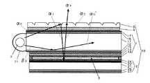
透明ガラス板の片面のみに設ける低屈折率の透明層は、その透明ガラス板よりも屈折率の低い層として設けることで図8に折れ線矢印α0'として示した如く、照明装置7等を介した側面からの入射光が透明ガラス板(セル基板)11の内部を伝送される際にその伝送光をガラス板11と透明層12との屈折率差を介し全反射させて透明ガラス板内に効率よく閉じ込め、それにより前記伝送光を対向の側面側(後方)に効率よく伝送することを目的とする。
【0014】
また前記した低屈折率の透明層は、セル基板として用いた場合に前記の伝送光が液晶層に入射して複屈折や散乱を受け、それにより伝送状態が部分的に変化して伝送光が減少したり不均一化することを防止して表示が暗くなることや、照明装置近傍での表示が後方においてゴースト化して表示品位を低下させることの防止なども目的とする。
【0015】
さらにカラーフィルタ等を配置した場合にそれによる伝送光の急激な吸収を防止して伝送光の減少を回避することも目的とする。上記した特開平5−158033号公報が教示する液晶表示装置の如く照明装置からの入射光が液晶層内を伝送されるものでは、液晶層で伝送光が散乱されて不均一な伝送状態となり、出射光の不均一化やゴーストを生じて表示像が見ずらくなりやすい。
【0016】
低屈折率の透明層は、透明ガラス板よりも屈折率の低い例えば無機系や有機系の低屈折率誘電体の如き適宜な材料を用いて真空蒸着方式やスピンコート方式などの適宜な方式で形成することができ、その材料や形成方法について特に限定はない。セル基板として用いる場合には電極形成時の安定性等の点より無機誘電体による低屈折率の透明層が好ましい。
【0017】
上記した全反射する角度範囲の拡大による後方への伝送効率等の点より透明層と透明ガラス板の屈折率差は、大きいほど有利であり、具体的には0.1以上であり、特に0.12〜0.5であることが好ましい。かかる程度の屈折率差ではセル基板に用いた場合にも外光による反射モードによる表示品位に殆ど影響しない。ちなみに当該屈折率差が0.1の場合、その界面での外光の反射率は0.1%以下でありその反射損による明るさやコントラストの低下は極めて小さいものである。
【0018】
図1に例示の如く低屈折率の透明層12の配置位置は、上記した伝送光の閉じ込め効果やセル基板とした場合の液晶層への浸入防止などの点より透明ガラス板11と導電層13の間とされる。また図例の如く透明ガラス板11と導電層13の間にカラーフィルタ層15を配置する場合には、カラーフィルタ層による伝送光の吸収損を防止する点よりそのカラーフィルタ層よりもガラス板11側に位置させることが好ましい。従って通例、低屈折率の透明層12は透明ガラス板11に直接設けられる。その場合、透明ガラス板における透明層の付設面は平滑なほど、よって透明層は平滑なほど伝送光の散乱防止に有利で好ましく、またセル基板とした場合には表示光への影響防止の点よりも好ましい。
【0019】
低屈折率の透明層の厚さは、薄すぎると波動のしみだし現象で上記した閉じ込め効果に薄れる場合があることより全反射効果の維持の点より厚いほど有利である。その厚さは全反射効果等の点より適宜に決定しうるが一般には波長380〜780nmの可視光に対する、特に短波長側の波長380nmの光に対する全反射効果等の点より、屈折率と層厚の積で算出される光路長に基づいて1/4波長(約100nm)以上、就中1/2波長(190nm)以上、特に1波長(380nm)以上の厚さであることが好ましく、さらには600nm以上の厚さであることが好ましい。
【0020】
透明ガラス板上に低屈折率透明層を介して設ける導電層は、セル基板とした場合の電極や光反射層ないしそれ兼用の電極、帯電防止や電磁波シールドなどのガラス基板の使用目的に応じた適宜なものであってよい。従って導電層は、例えばITO(インジウム・スズ酸化物)等による透明層や金属薄膜等による光反射型などの不透明層として従来に準じた適宜な材料にて形成することができる。
【0021】
本発明によるガラス基板は、従来に準じた各種の目的に用いることができ、特に上記したように側面入射光の後方への伝送効率に優れることより液晶セルにおけるセル基板などの如く、光を側面より入射させて後方へ伝送する用途に好ましく用いうる。その実用に際しては必要に応じて例えば図1の例の如くカラーフィルタ層15やガスバリア層16、ハードコート層17などの適宜な機能層の1層又は2層以上を適宜な位置に設けることができる。
【0022】
前記のカラーフィルタ層15は液晶表示等のカラー化などを目的に設けられ通例、上記した如く低屈折率透明層12と導電膜13の間に設けられる。また液晶セル基板とする場合には液晶を配向させるためのラビング処理膜等からなる配向膜14を設けることもできる。配向膜は通常、図例の如く電極とした導電膜13の上に形成される。なおセル基板とする場合、ガスバリア層は図例の如く通例、セルの外側となる位置に設けられ、ハードコート層はセルの外側となる表面に設けられる。
【0023】
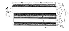
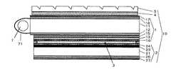
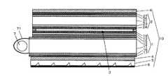
本発明による液晶表示装置は、視認側と背面側のセル基板をそれらに設けた電極の側を対向させて配置した間に液晶を挟持してなる液晶セルを少なくとも具備する液晶表示パネルを有してなり、かつ前記の視認側と背面側のセル基板の一方又は両方に上記した低屈折率透明層付設のガラス基板を用いたものである。その例を図2〜4に示した。10が液晶表示パネルで、1が低屈折率透明層付設のガラス基板からなる視認側基板、2が他方となる背面側の基板、3が液晶層である。また21はセル基板、23は電極、24は配向膜、26はガスバリア層、27はハードコート層である。
【0024】
液晶表示パネル10としては、前記した低屈折率透明層付設のガラス基板をセル基板の少なくとも一方に用いてなる液晶セルを有する点を除いてその種類につき特に限定はなく、適宜なものを用いることができる。ちなみに前記した液晶表示パネルの具体例としては、液晶の配向形態に基づいてTN型液晶表示パネルやSTN型液晶表示パネル、垂直配向型表示パネルやHAN型表示パネル、OCB型表示パネルの如きツイスト系や非ツイスト系、ゲストホスト系や強誘電性液晶系のもの、光拡散を利用したものなどがあげられる。また液晶の駆動方式も例えばアクティブマトリクス方式やパッシブマトリクス方式などの適宜なものであってよい。その液晶の駆動は通例、図2の例の如く一対のセル基板1、2の内側に設けた電極13、23を介して行われる。
【0025】
なお視認側又は背面側のセル基板に本発明によるガラス基板を用いない場合、その他方のセル基板にはガラスや樹脂などの適宜な材料からなるものを用いうる。軽量性の点よりは樹脂基板の使用が有利である。ちなみにその樹脂の例としてはアセテート系樹脂やポリエステル系樹脂、ポリエーテルスルホン系樹脂やポリカーボネート系樹脂、ポリアミド系樹脂やポリイミド系樹脂、ポリオレフィン系樹脂やアクリル系樹脂、ポリエーテル系樹脂やポリ塩化ビニル、スチレン系樹脂やノルボルネン系樹脂、あるいはアクリル系やウレタン系、アクリルウレタン系やエポキシ系、シリコーン系等の熱硬化型ないし紫外線硬化型の樹脂などがあげられる。
【0026】
また前記した他方のセル基板は、照明光や表示光等を透過させる必要のある場合には透明な基板であることを要するが、例えばセル内に反射層兼用の電極を設けてなる反射型液晶セルの如く光を透過する必要のない場合には不透明な基板であってもよい。ちなみに図2の例による液晶表示パネルでは、視認側と背面側の両セル基板11、21及びそれらの内側に設けた両電極13、23が透明層よりなる透過型の液晶セルからなり、その視認側基板に本発明によるガラス基板1を用いてなる液晶セルの背面側に反射層6を配置したフロントライト式の透過・反射両用型のものからなる。
【0027】
また図3の例による液晶表示パネルでは背面側基板の内側に設けた電極23’が光反射層兼用の金属薄膜よりなる反射型の液晶セルからなり、フロントライト式の透過・反射両用型のものからなる。従って図3の透過・反射両用型液晶表示パネルの場合、図例では背面側基板に透明基板21を用いているが光を透過する必要がないので前記した如く不透明な基板であってもよい。またその基板にガス遮蔽性や耐擦傷性のものを用いた場合には図例におけるガスバリア層26やハードコート層27を省略し得て、より薄型化等をはかりうる。
【0028】
一方、図4の例による液晶表示パネルでは、視認側と背面側の両セル基板21、11及びそれらの内側に設けた両電極23、13が透明層よりなる透過型の液晶セルからなり、その背面側基板に本発明によるガラス基板1が用いられている。なお図例では液晶セルの背面側に反射層6を配置してバックライト式の透過・反射両用型液晶表示パネルとされているが、その反射層を配置しないことで透過型のものとすることもできる。
【0029】
液晶表示装置の形成に際しては必要に応じ、液晶セルの片側又は両側に偏光板や位相差板、光拡散層や光路変換手段等の適宜な光学層の1層又は2層以上を設けることができ、また液晶表示パネルの1又は2以上の側面に照明装置を設けることもできる。さらに本発明によるガラス基板以外のセル基板にカラーフィルタ層を設けることもできる。その場合、カラーフィルタ層は通常、セル基板における基板と電極の間に設けられる。またカラーフィルタ層は一般に視認側基板に設けられるが、これに限定されない。なお図例において4が偏光板、5が光路変換手段、7が照明装置である。
【0030】
前記した偏光板は直線偏光を利用した表示の達成を目的とし、位相差板は液晶の複屈折性による位相差の補償等による表示品位の向上などを目的とする。また光拡散層は、表示光の拡散による表示範囲の拡大や光路変換手段を介した輝線状発光の平準化による輝度の均一化、液晶表示パネル内の伝送光の拡散による光路変換手段への入射光量の増大などを目的とする。一方、光路変換手段は、液晶表示パネルの側面に配置した照明装置からの入射光ないしそのパネル内の伝送光を光路制御して液晶表示パネルの厚さ方向に光路変換し表示光として利用することを目的とする。
【0031】
偏光板としては、適宜なものを用いることができ特に限定はない。高度な直線偏光の入射による良好なコントラスト比の表示を得る点などよりは、例えばポリビニルアルコール系フィルムや部分ホルマール化ポリビニルアルコール系フィルム、エチレン・酢酸ビニル共重合体系部分ケン化フィルムの如き親水性高分子フィルムにヨウ素や二色性染料等の二色性物質を吸着させて延伸したものからなる吸収型偏光フィルムやその片側又は両側に透明保護層を設けたものなどの如く偏光度の高いものが好ましく用いうる。
【0032】
前記した透明保護層の形成には、上記の樹脂基板で例示した樹脂などの適宜なものを用いることができ、透明性や機械的強度、熱安定性や水分遮蔽性などに優れるものが好ましく用いられる。透明保護層は、フィルムとしたものの接着方式や樹脂液等の塗布方式などにより付与することができる。用いる偏光板、特に視認側の偏光板は、外光の表面反射による視認阻害の防止を目的にノングレア処理や反射防止処理を施したものであってもよい。
【0033】
前記のノングレア処理は、サンドブラスト方式やエンボス加工方式等の粗面化方式、シリカ等の透明粒子の配合方式などの種々の方式で表面を微細凹凸構造化することにより施すことができる。反射防止処理は、干渉性の蒸着膜を形成する方式などにて施すことができる。またノングレア処理や反射防止処理は、前記の表面微細凹凸構造や干渉膜を付与したフィルムの接着方式などにても施すことができる。なお偏光板は、図2,4の例の如く液晶セルの両側に設けることもできるし、図3の例の如く液晶セルの片側にのみ設けることもできる。
【0034】
一方、位相差板としても上記の樹脂基板で例示したもの等の適宜な樹脂からなるフィルムを一軸や二軸等の適宜な方式で延伸処理してなる複屈折性フィルム、ネマチック系やディスコティック系等の適宜な液晶ポリマーの配向フィルムやその配向層を透明基材で支持したものなどの適宜なものを用いることができ、熱収縮性フィルムの加熱収縮力の作用下に厚さ方向の屈折率を制御したものなどであってもよい。補償用の位相差板は通例、視認側又は/及び背面側の偏光板と液晶セルの間に必要に応じて配置され、その位相差板には波長域などに応じて適宜なものを用いうる。また位相差板は、位相差等の光学特性の制御を目的に2層以上を重畳して用いることもできる。
【0035】
また光拡散層についても前記のノングレア層に準じた表面微細凹凸構造を有する塗工層や拡散シートなどによる適宜な方式にて設けることができる。光拡散層は、透明粒子配合の粘着層として偏光板や位相差板等の光学層の接着を兼ねる層として形成することもでき、それにより薄型化を図ることもできる。その粘着層の形成には、ゴム系やアクリル系、ビニルアルキルエーテル系やシリコーン系、ポリエステル系やポリウレタン系、ポリエーテル系やポリアミド系、スチレン系などの適宜なポリマーをベースポリマーとする粘着剤などを用いうる。
【0036】
就中アクリル酸ないしメタクリル酸のアルキルエステルを主体とするポリマーをベースポリマーとするアクリル系粘着剤の如く透明性や耐候性や耐熱性などに優れるものが好ましく用いられる。また粘着層に配合することのある前記の透明粒子としては、例えば平均粒径が0.5〜20μmのシリカやアルミナ、チタニアやジルコニア、酸化錫や酸化インジウム、酸化カドミウムや酸化アンチモン等からなる導電性のこともある無機系粒子、架橋又は未架橋のポリマー等からなる有機系粒子などの適宜なものを1種又は2種用いることができる。
【0037】
上記したように光路変換手段は、図8の折れ線矢印α0、α1で示した如く液晶表示パネル10の側面に配置した照明装置7からの入射光ないしその伝送光を反射して当該パネルの厚さ方向に光路変換させ照明光(表示光)として利用することを目的とする点より、図2〜4の例の如く液晶表示パネル10における視認側基板又は背面側基板の一方の外側に配置され、それによりフロントライト又はバックライトが形成される。
【0038】
光路変換手段5は、図例の如く照明装置7からの入射光を反射して所定方向に光路変換しうる適宜な形態のものとして形成することができる。光路変換等を介して正面方向への指向性に優れる表示光を得る点よりは、照明装置を配置した側面すなわち入射側面と対面する光路変換斜面を具備する光路変換手段、特に断面略三〜五角形のプリズム状凸凹からなる光路変換斜面を具備する光路変換手段が好ましい。
【0039】
上記した正面方向への指向性等の点より好ましい前記光路変換斜面は、その液晶表示パネル平面に対する傾斜角が35〜48度、就中38〜45度、特に40〜44度のものである。また光路変換手段は、薄型化の点より前記の光路変換斜面が繰返し構造として形成されているものが好ましい。さらに光路変換斜面は、突出(凸)形態にても形成しうるが、耐擦傷性の向上による斜面機能の維持の点よりは溝(凹)形態に形成されていることが斜面等が傷付きにくくて有利である。液晶表示パネルの2側面以上に照明装置を配置して2以上の入射側面を有する場合には、例えば断面二等辺三角形による2面の光路変換斜面の如く、その入射側面の数と位置に対応して光路変換斜面を有する光路変換手段としたものが好ましく用いられる。
【0040】
図2〜4に例示の透過・反射両用型の液晶表示装置では、図8の折れ線矢印α2の如く光路変換手段層5を介して表示光α3を見る必要のある場合があり、その場合には表示光の良視認性などの点より図例の如く前記した光路変換斜面の間に緩斜面ないし平坦面を有する構造の光路変換手段が好ましい。従って例えば光路変換斜面と緩斜面からなる断面三角形のプリズム状凹凸が隣接して繰り返す構造の光路変換手段からなるときには、その緩斜面のパネル平面に対する傾斜角が10度以下、就中5度以下、特に3度以下であることが好ましい。またその最寄り緩斜面間の傾斜角の差は1度以内、就中0.3度以内等の小さいことが好ましい。
【0041】
前記した光路変換斜面を有する構造の光路変換手段とすることにより、その光路変換斜面を介し側面からの入射光ないしその伝送光を反射させて正面方向の指向性よく光路変換でき明るさを透過と反射の両モードに有利な状態に容易にバランスさせることができる。しかし特開平5−158033号公報におけるように粗面を介した散乱反射方式の場合、表示に利用できる光は、散乱で全反射条件から外れてパネルより出射する正面方向より大きく傾斜した光であるから表示に有効利用しにくく正面方向での表示が暗くなり、粗面型反射板による散乱を強くすると反射モードでの正面方向の光量を低減させて表示に不利となる。従って斯かる粗面散乱反射方式では透過と反射の両モードでの明るさをバランスさせることが難しい。
【0042】
光路変換手段は、照明装置の波長域に応じそれに透明性を示す適宜な材料にて形成しうる。ちなみに可視光域では上記の樹脂基板で例示した樹脂やガラスなどがあげられる。複屈折を示さないかそれの小さい材料で形成した光路変換手段が好ましい。また界面反射でパネル内部に閉じ込められて出射できない損失光量を抑制し側面入射光ないしその伝送光を光路変換手段の光路変換斜面に効率よく供給する点より、ガラス基板における低屈折率の透明層よりも高屈折率、就中0.05以上、特に0.1以上高い屈折率の光路変換手段であることが好ましい。
【0043】
光路変換手段は、切削法にても形成でき適宜な方法で形成することができる。
量産性等の点より好ましい製造方法としては、例えば熱可塑性樹脂を所定の形状を形成しうる金型に加熱下に押付て形状を転写する方法、加熱溶融させた熱可塑性樹脂あるいは熱や溶媒を介して流動化させた樹脂を所定の形状に成形しうる金型に充填する方法、熱や紫外線ないし放射線等で重合処理しうる液状樹脂を所定の形状を形成しうる型に充填ないし流延して重合処理する方法などがあげられる。従って光路変換手段は、セル基板等に直接その所定形態を付与して形成することもできるし、所定の形態を付与した透明シート等として形成することもできる。光路変換手段の厚さは、適宜に決定しうるが一般には薄型化などの点より300μm以下、就中5〜200μm、特に10〜100μmとされる。
【0044】
光路変換手段は、図2〜4に例示の如く光路変換手段を形成した面を外側にして配置することがその光路変換斜面を介した反射効率、ひいては側面入射光の有効利用による輝度向上の点などより好ましい。光路変換手段を前記の如く透明シート等として独立に形成した場合には、その透明シート等をガラス基板における低屈折率の透明層よりも高い屈折率の接着層、就中その透明シート等と可及的に等しい屈折率の接着層を介して液晶表示パネルに接着することが前記の点などより好ましい。
【0045】
従って前記接着層の屈折率は、上記した光路変換手段に準じうる。その接着層は、適宜な透明接着剤にて形成でき、その接着剤の種類について特に限定はない。接着処理作業の簡便性などの点よりは粘着層による接着方式が好ましい。その粘着層については上記に準じることができ、上記した光拡散型の粘着層とすることもできる。
【0046】
液晶表示パネルの側面に配置する照明装置は、液晶表示装置の照明光として利用する光を液晶表示パネルの側面から入射させることを目的とする。これによりパネルに配置する光路変換手段との組合せにて液晶表示装置の薄型軽量化を図ることができる。ちなみに上記の図2〜4に示した液晶表示パネルでは、それらに準じた図5〜7に示したサイドライト型導光板83使用の透過・反射両用型の液晶表示パネルとの対比より明らかな如く、光路変換手段5とサイドライト型導光板83との厚さの差がそのまま液晶表示装置の厚さの差として現れる。なお図5〜7において25はカラーフィルタ層、8は照明装置で81が光源、82がそのホルダであり、他の符号は図2〜4に準じる。
【0047】
照明装置からの入射光の後方への伝送効率の点より照明装置の好ましい配置位置は、図2〜4に例示の如く本発明によるガラス基板1からなり、かつ光路変換手段を設けた側のセル基板の側面である。またその場合に照明装置からの入射光の液晶層への入射を防止する点より照明装置の好ましい配置方式は、照明装置を配置するセル基板1の側面を他方のセル基板2が形成する側面よりも突出させる方式である。従って視認側と背面側のセル基板は、平面寸法が相違していてもよく同じである必要はない。また上記したように視認側と背面側のセル基板の厚さは、相違していてもよく同じである必要はない。
【0048】
前記により図8に折れ線矢印β0、α0’で例示した如くガラス基板1に設けた低屈折率の透明層12を介し、照明装置7を介した側面からの入射光β0が透明ガラス板11の内部を伝送される際にその伝送光をガラス板11と透明層12との屈折率差を介し全反射させて透明ガラス板内に効率よく閉じ込め、それにより前記伝送光α0’を対向の側面側(後方)に効率よく伝送して照明装置から遠い位置における光路変換手段5の光路変換斜面にも伝送光を均等性よく供給し、その斜面による反射を介し折れ線矢印α1、α2、α3として示した如く光路変換して表示画面全体における明るさの均一性を向上させることができる。
【0049】
前記の結果、照明装置からの入射光ないしその伝送光を後方に効率よく伝送しつつ、その伝送光を光路変換手段を介し液晶表示パネルの視認方向に効率よく光路変換して液晶表示に利用でき、照明装置の側面配置と薄さに優れる光路変換手段とでフロントライト機構やバックライト機構を形成できて薄さと軽量性に優れ明るくて表示品位に優れる透過型や透過・反射両用型の液晶表示装置を形成することができる。
【0050】
前記において照明装置を配置するセル基板が低屈折率の透明層を有しないものである場合には図9に折れ線矢印β、β1、β2、α0”で例示した如く、照明装置7を介した側面からの入射光β0が基板21の内部を伝送される際にその伝送光がカラーフィルタ層25や液晶層3等に入射し、反射層兼用電極23’を介した反射光β2も液晶層3やカラーフィルタ層25等を再透過することとなって上記した如く後方に伝送される光α0”が大きく低下し、照明装置から遠離るほど明るさが低下して表示画面全体での輝度のバラツキが大きくなる。
【0051】
照明装置としては適宜なものを用いることができ、例えば(冷,熱)陰極管等の線状光源、発光ダイオード等の点光源やそれを線状や面状等に配列したアレイ体、あるいは点光源と線状導光板を組合せて点光源からの入射光を線状導光板を介し線状光源に変換するようにした照明装置などが好ましく用いうる。照明装置は、液晶表示パネルにおける1又は2以上の側面に配置することができる。照明装置を2以上の側面に配置する場合、その複数の側面は対向する側面の組合せであってもよいし、縦横に交差する側面の組合せであってもよく、それらを併用した3側面以上の組合せであってもよい。
【0052】
照明装置は、その点灯モードでの視認を可能とするものであり、透過・反射両用型の液晶表示装置の場合に外光による反射モードにて視認するときには点灯の必要がないので、その点灯・消灯を切り替えうるものとされる。その切り替え方式には任意な方式を採ることができ、従来方式のいずれも採ることができる。なお照明装置は、発光色を切り替えうる異色発光式のものであってもよく、また異種の照明装置を介して異色発光させうるものとすることもできる。
【0053】
図例の如く照明装置7に対しては、必要に応じ発散光を液晶表示パネルの側面に導くためにそれを包囲する光源ホルダ71などの適宜な補助手段を配置した組合せ体とすることもできる。光源ホルダとしては、例えば高反射率の金属薄膜を付設した樹脂シートや白色シートや金属箔などの如く、少なくとも照明装置側が光を反射する適宜な反射シートを用いうる。光源ホルダは、その端部を液晶表示パネルのセル基板の上下面の端部に接着する方式などにて照明装置の包囲を兼ねる保持手段として利用することもできる。
【0054】
図2、4に例示した如く液晶表示装置には必要に応じ適宜な位置に光反射層6を配置することができる。斯かる光反射層は、図2の例ではフロントライトの反射反転を目的とし、図4の例では光路変換手段よりの漏れ光を反射反転させて再入射させることによる光利用効率の向上や液晶セル側からの光を反射して透過・反射両用型の液晶表示装置の形成を目的とする。光反射層は、従来に準じた白色シートなどの適宜なものにて形成することができる。
【0055】
就中、例えばアルミニウムや銀、金や銅やクロム等の高反射率の金属ないしその合金の粉末をバインダ樹脂中に含有させた塗工層、前記の金属等や誘電体多層膜を真空蒸着方式やスパッタリング方式等の適宜な薄膜形成方式で付設してなる金属薄膜層、前記の塗工層や付設層をフィルム等からなる基材で支持した反射シート、金属箔などからなる高反射率の光反射層が好ましく、透過・反射両用型の液晶表示装置を形成する場合に特に好ましい。
【0056】
設ける光反射層は、光拡散機能を示すものであってもよい。拡散反射面にて反射光を拡散させることにより正面方向への指向性の向上を図ることができ、また粗面化による場合には密着によるニュートンリングの発生を防止して視認性を向上させることができる。従って光反射層は、光路変換手段の外側に単に重ね置いた状態にあってもよいし、接着方式や蒸着方式などで密着配置された状態にあってもよい。光路変換手段の斜面に光反射層を密着配置した場合には、反射効果の向上で漏れ光をほぼ完全に防止でき、視角特性や輝度をより向上させることができる。
【0057】
光拡散型の反射層の形成は、例えばサンドブラストやマット処理等による表面の粗面化方式や、粒子添加方式などの適宜な方式で表面を微細凹凸構造としたフィルム基材等にその微細凹凸構造を反映させた光反射層を設ける方式などにより行うことができる。その表面の微細凹凸構造を反映させた微細凹凸構造の光反射層の形成は、例えば真空蒸着方式やイオンプレーティング方式、スパッタリング方式等の蒸着方式やメッキ方式などの適宜な方式で金属をフィルム基材等の表面に付設する方法などにより行うことができる。
【0058】
上記した液晶表示装置によれば、入射側面よりの入射光の殆どが液晶表示パネル、特にそのセル基板を介し屈折の法則による反射を介して後方に伝送されパネル表面よりの出射(漏れ)が防止されつつ、光路変換手段の光路変換斜面に入射した光が効率よく視認方向に垂直指向性よく光路変換され、他の伝送光は全反射にて後方に更に伝送され後方における光路変換斜面に入射し効率よく視認方向に垂直指向性よく光路変換されてパネル表示面の全面において明るさの均一性に優れる表示を達成することができる。従って照明装置からの光を効率よく利用して明るくて見やすく表示品位に優れる透過型や透過・反射両用型の液晶表示装置を形成することができる。
【0059】
なお本発明において上記した液晶表示装置を形成する光路変換手段や液晶セル、偏光板や位相差板等の光学素子ないし部品は、全体的又は部分的に積層一体化されて固着されていてもよいし、分離容易な状態に配置されていてもよい。界面反射の抑制によるコントラストの低下防止などの点よりは固着状態にあることが好ましい。
【0060】
前記の固着密着処理には、粘着剤等の適宜な透明接着剤を用いることができ、その透明接着層に上記した透明粒子等を含有させて拡散機能を示す接着層などとすることもできる。また前記の光学部材、特に視認側のそれには例えばサリチル酸エステル系化合物やベンゾフェノン系化合物、ベンゾトリアゾール系化合物やシアノアクリレート系化合物、ニッケル錯塩系化合物等の紫外線吸収剤で処理する方式などにより紫外線吸収能をもたせることもできる。
【0061】
【実施例】
参考例1
予め所定形状に加工した金型にアクリル系の紫外線硬化型樹脂をスポイトにて滴下充填し、その上に厚さ60μmのポリカーボネートフィルムを静置しゴムローラで密着させて余分な樹脂と気泡を除去しメタルハライドランプにて紫外線を照射して硬化処理した後、金型から剥離し所定寸法に裁断しそれをポリカーボネートフィルムより剥離して屈折率1.51の光路変換手段シートを得、その光路変換手段を有しない面に屈折率1.51の粘着層を付設して透明シートを得た。この透明シートは、幅40mm、長さ30mmであり、稜線が幅方向にわたり21度の角度で傾斜するプリズム状凹部を210μmのピッチで連続して有し、その光路変換斜面の傾斜角が約42度で急斜面との頂角が70度、光路変換斜面の基準平面に対する投影幅が10〜16μmで、平坦部の面積が光路変換斜面と急斜面の基準平面に対する投影合計面積の10倍以上のものからなる。
【0062】
参考例2
異なる金型を用いて参考例1に準じ光路変換手段そのものからなる粘着層付の透明シートを得た。この透明シートは、幅40mm、長さ30mmであり、稜線が幅方向にわたり21度の角度で傾斜するプリズム状凹部を210μmのピッチで連続して有し、その光路変換斜面の傾斜角が約42度で急斜面との頂角が70度、光路変換斜面の基準平面に対する投影幅が13〜17μmで、平坦部の面積が光路変換斜面と急斜面の基準平面に対する投影合計面積の10倍以上のものからなる。
【0063】
実施例1
厚さ1.2mm、屈折率1.52の透明な白板ガラスの表面を中性洗剤と純水で順次洗浄してスピンコータで水を除去した後、アルゴン雰囲気中でプラズマ処理してその片面にフッ化マグネシウムを電子ビーム加熱にて真空蒸着し厚さ600nm、屈折率1.38の低屈折率透明層を形成し、その上に赤、青、緑のストライプ状のカラーフィルタ層、及びスパッタリングによるITO透明導電層(電極)を順次形成してガラス基板を得た。
【0064】
実施例2
低屈折率透明層の厚さを300nmとしたほかは実施例1に準じてガラス基板を得た。
【0065】
実施例3
低屈折率透明層の厚さを100nmとしたほかは実施例1に準じてガラス基板を得た。
【0066】
参考例3
フッ化マグネシウムに代えて酸化ケイ素を用いて屈折率が1.46の低屈折率透明層を形成したほかは実施例1に準じてガラス基板を得た。
【0067】
参考例4
低屈折率透明層を設けないほかは実施例1に準じてガラス基板を得た。
【0068】
参考例5
低屈折率透明層とカラーフィルタ層を設けないほかは実施例1に準じて厚さを0.2mmとしたガラス基板を得た。
【0069】
実施例4
実施例1のガラス基板からなる視認側基板及び参考例5のガラス基板からなる背面側基板における透明電極上にポリビニルアルコール溶液をスピンコートしその乾燥膜をラビング処理し、それらのラビング面をラビング方向が直交するように対向させて球形ガラスビーズよりなるギャップ調節材を配し、周囲をシール材で固定したのち液晶(メルク社製、ZLI−4792)を注入してTN型液晶セルを形成し、その視認側に反射防止処理とノングレア処理を施した偏光板(日東電工社製、NPF EGW1145DU)を、背面側に反射型偏光板(日東電工社製、NPF EG3228GR)を貼着してノーマリーホワイトの反射型液晶表示パネルを得た。そのパネルサイズは幅45mm、長さ34mmで、その長さ方向の視認側基板の一側面が背面側基板よりも2mm突出したものである。なお前記の背面側基板における透明電極は、ラビング処理前にエッチングして2分割した。
【0070】
次に前記パネルの視認側基板の突出側面に冷陰極管を配置し、銀蒸着のポリエステルフィルムで包囲してフィルム端部を基板の上下面に両面粘着テープで接着し冷陰極管を保持固定した。またパネルの視認側上面に参考例1で得た透明シートをその粘着層を介し接着して光路変換手段を配置し、透過・反射両用型の液晶表示装置を得た。
【0071】
実施例5
実施例1のガラス基板に代えて実施例2のガラス基板を視認側基板に用いたほかは実施例4に準じて透過・反射両用型の液晶表示装置を得た。
【0072】
実施例6
実施例1のガラス基板に代えて実施例3のガラス基板を視認側基板に用いたほかは実施例4に準じて透過・反射両用型の液晶表示装置を得た。
【0073】
比較例1
実施例1のガラス基板に代えて参考例3のガラス基板を視認側基板に用いたほかは実施例4に準じて透過・反射両用型の液晶表示装置を得た。
【0074】
比較例2
実施例1のガラス基板に代えて参考例4のガラス基板を視認側基板に用いたほかは実施例4に準じて透過・反射両用型の液晶表示装置を得た。
【0075】
実施例7
参考例5のガラス基板を視認側基板に用い、かつ実施例1のガラス基板を背面側基板に用いたほかは実施例4に準じてTN型液晶セルを形成し、その両側に偏光板(上記のNPFEGW1145DU)を貼着してノーマリーホワイトの透過型液晶表示パネルを得た。なおパネルでは背面側基板の一側面を視認側基板よりも2mm突出させ、また視認側基板の透明電極をエッチングで2分割した。次に前記パネルの背面基板の突出側面に冷陰極管を配置し、銀蒸着のポリエステルフィルムで包囲してフィルム端部を基板の上下面に両面粘着テープで接着し冷陰極管を保持固定した。またパネルの背面側下面に参考例2で得た透明シートをその粘着層を介し接着して光路変換手段を配置し、透過型の液晶表示装置を得た。
【0076】
比較例3
実施例1のガラス基板に代えて参考例4のガラス基板を背面側基板に用いたほかは実施例7に準じて透過型の液晶表示装置を得た。
【0077】
評価試験
実施例、比較例で得た液晶表示装置について暗室にて液晶セルに電圧を印加しない状態で冷陰極管を点灯させ、その点灯モードによる入射側面より10mm、中央部、対向端より10mmの位置での正面輝度を輝度計(トプコン社製、BM7)にて視野1度の条件で調べた。また実施例4〜6、比較例1〜2で得た透過・反射両用型の液晶表示装置について暗室にて冷陰極管を点灯せず、20度の方位角で配置したリング状照明装置による外光モードでの中央部での正面輝度も調べた。
【0078】
前記の結果を次表に示した。
正面輝度(cd/m2)
点灯モード外光モード
入射側面部 中央部 対向端部中央部
実施例4 45 41 38 153
実施例5 42 36 31 161
実施例6 41 34 30 160
比較例1 42 34 31 168
比較例2 40 22 11 172
実施例7 327 346 319 −
比較例3 237 121 63 −
【0079】
表より点灯モードにおいて、実施例では明るくてそのバラツキが小さいが、比較例では暗くてそのバラツキも大きいことがわかる。また実施例4〜6より低屈折率透明層の厚さが大きくなるほど入射側面部での特性が改善されて明るさの均一性が高くなり、基板との屈折率差が大きいほど明るさに優れることがわかる。さらに反射モードでは比較例との差が小さいことより低屈折率透明層の付加による反射モードへの影響が小さいこともわかる。
【0080】
一方、液晶セルに電圧を印可して画面の半分を表示状態として観察したが実施例4〜7では点灯モード及び実施例4〜6では反射モードにおいてもいずれの場合も特に問題なく良好な表示であった。しかし比較例の点灯モードでは暗くてそのバラツキが大きく非常に見ずらい表示であった。以上より本発明にては低屈折率の透明層を付加したガラス基板の使用でカラーフィルタによる吸収等も防止して均一な輝度分布の透過型や透過・反射両用型の液晶表示装置を形成でき、光路変換手段及び照明装置の側面配置との組合せ方式にて導光板の使用による嵩高化、高重量化を回避しつつ薄型軽量化を達成して表示品位の良好な液晶表示装置を形成できることがわかる。
【図面の簡単な説明】
【図1】ガラス基板例の断面図
【図2】液晶表示装置例の断面図
【図3】他の液晶表示装置例の断面図
【図4】さらに他の液晶表示装置例の断面図
【図5】従来例の断面図
【図6】他の従来例の断面図
【図7】さらに他の従来例の断面図
【図8】実施例による光路の説明図
【図9】従来例による光路の説明図
【符号の説明】
10:液晶表示パネル
1、2:ガラス基板
11、21:透明ガラス板
12:低屈折率の透明層
13、23:導電膜(透明電極)
23’:反射層兼用電極
14、24:配向膜
15:カラーフィルタ層
16、26:ガスバリア層
17、27:ハードコート層
3:液晶層
4:偏光板
5:光路変換手段
6:光反射層
7:照明装置[0001]
TECHNICAL FIELD OF THE INVENTION
The present invention relates to a glass substrate capable of efficiently transmitting incident light from the side to the rear, and a transmissive or transmissive / reflective liquid crystal display device using the same for a cell substrate.
[0002]
BACKGROUND OF THE INVENTION
As liquid crystal display devices are required to be thinner and lighter for the purpose of suppressing the increase in weight associated with the increase in the size of TVs and personal computer screens, and reducing the size and weight of mobile personal computers and mobile phones, the examples illustrated in FIGS. It is difficult to reduce the thickness and weight of the conventional sidelight type
[0003]
In view of the above, an illuminating device is arranged on the side surface of the liquid crystal display panel, and the illumination light from the side surface is totally reflected by the cell substrate on the viewing side while transmitting the entire surface of the panel, and the reflected light is reflected by the rough surface type reflector. A reflection-type liquid crystal display device that has been scattered and used for display has been proposed (Japanese Patent Laid-Open No. 5-158033). The purpose of this is to achieve the reduction in thickness and weight by omitting the light guide plate by sharing the role of the side light type light guide plate with the liquid crystal display panel. The light transmission is performed by the entire liquid crystal display panel, but the cell substrate of the liquid crystal cell seems to be the center.
[0004]
However, with conventional glass substrates that satisfy the required performance such as transparency, heat resistance, chemical resistance, surface smoothness and gas barrier properties, the light transmission efficiency is poor and the display becomes darker as the distance from the lighting device increases. As a result, it was found that there was a problem that the difference in brightness on the panel surface was large.
[0005]
[Technical Problem of the Invention]
The present invention obtains a glass substrate having excellent transmission efficiency to the rear of light incident from the side while making use of the advantages of thin and light weight, and has excellent display quality and transmission type transmission and transmission / transmission characteristics. It is an object to develop a reflection-use liquid crystal display device.
[0006]
[Means for solving problems]
The present invention is a single side of a transparent glass plate.onlyAt least a conductive layer through a transparent layer having a refractive index lower than that of the plate, and the refractive index difference between the low refractive index transparent layer and the transparent glass plate is 0.1 or more, and the low refractive index transparent layer An optical path length based on the product of the thickness and refractive index of the glass substrate is 100 nm or more, and the liquid crystal is disposed between the viewing side and the back side cell substrates facing each other on the electrode side provided on them. A liquid crystal display device comprising a liquid crystal display panel having at least a liquid crystal cell sandwiched between the glass substrate and one or both of the viewing-side and back-side cell substrates comprising the glass substrate. It is to provide.
[0007]
【The invention's effect】
According to the glass substrate of the present invention, incident light from the side surface can be efficiently transmitted in the opposite side direction (backward) by confining the transparent layer having a low refractive index in the substrate by total reflection, and the weight increase is also transparent with a low refractive index. It is excellent in thinness and lightness because it is a degree of addition of a layer. As a result, by using the glass substrate as a cell substrate to form a liquid crystal cell, incident light from an illuminating device disposed on the side surface of the liquid crystal display panel can be efficiently transmitted rearward through the substrate, and the transmitted light. By changing the optical path in the viewing direction through an appropriate optical path conversion means, the entire screen is bright, and good display quality with excellent brightness uniformity is achieved. Further, it is possible to form a liquid crystal display device that is excellent in thinness due to the side arrangement of the lighting device.
[0008]
In the above, if there is no transparent layer having a low refractive index, the transmission light in the panel is incident on the liquid crystal layer or a color filter layer disposed adjacent to the liquid crystal layer, and is absorbed when it enters the polarizing plate due to birefringence by the liquid crystal layer. As the components increase or the light transmission by the color filter layer significantly reduces the transmission efficiency in the rear, the screen becomes darker as the distance from the illumination device increases, and the luminance uniformity is greatly impaired, resulting in a display that is difficult to see.
[0009]
DETAILED DESCRIPTION OF THE INVENTION
The glass substrate according to the present invention is a single side of a transparent glass plate.onlyAt least a conductive layer through a transparent layer having a refractive index lower than that of the plate, and the refractive index difference between the low refractive index transparent layer and the transparent glass plate is 0.1 or more, and the low refractive index transparent layer The optical path length based on the product of the thickness and the refractive index is 100 nm or more. FIG. 1 shows an example of the glass substrate 1. 11 is a transparent glass plate, 12 is a transparent layer having a low refractive index, 13 is a conductive layer, 14 is an alignment film, 15 is a color filter layer, 16 is a gas barrier layer, and 17 is a hard coat layer.
[0010]
As the transparent glass plate, an appropriate one according to a conventional cell substrate or the like can be used, and there is no particular limitation. Among them, those having excellent transparency such as white plate glass with respect to blue plate glass are preferable from the viewpoints of transmission of illumination light and transmission of display light. In addition, a material excellent in optical isotropy, surface smoothness, and the like is preferable from the viewpoint of reducing light loss by suppressing birefringence in the light transmission direction and thickness direction as much as possible.
[0011]
There is no limitation in particular about the thickness of a transparent glass plate, According to the intensity | strength etc. according to the intended purpose, it can determine suitably. In the case of a cell substrate, a thickness of 20 μm to 5 mm, especially 50 μm to 2 mm, especially 100 μm to 1 mm is generally used from the standpoint of balance between liquid crystal encapsulation strength, light transmission efficiency, and thin and light weight. In particular, when used as a transmission substrate for incident light from an illuminating device, the larger the cross-sectional area is, the more advantageous in terms of incident efficiency, transmission efficiency, and the like.
[0012]
On the other hand, it is more advantageous that the thickness is thinner than the point of reducing the thickness and weight. The transparent glass plate may be the same thickness plate, or may be partially different in thickness. When used as the above transmission board, for example, a part of which the thickness is partially different, such as a wedge shape in the transmission direction, is the incident efficiency of the transmitted light to the inclined optical path changing means. Sometimes it is more advantageous than improvement.
[0013]
One side of transparent glass plateonlyThe low refractive index transparent layer provided in FIG. 8 is provided as a layer having a refractive index lower than that of the transparent glass plate.0As shown as', when the incident light from the side surface through the
[0014]
In addition, the low refractive index transparent layer described above, when used as a cell substrate, the transmission light is incident on the liquid crystal layer and undergoes birefringence and scattering. Another object is to prevent the display from becoming darker due to reduction or non-uniformity, and to prevent the display in the vicinity of the lighting device from being ghosted in the rear to lower the display quality.
[0015]
It is another object of the present invention to prevent a decrease in transmitted light by preventing sudden absorption of transmitted light when a color filter or the like is disposed. In the case where the incident light from the illuminating device is transmitted through the liquid crystal layer as in the liquid crystal display device taught in the above-mentioned JP-A-5-158033, the transmission light is scattered by the liquid crystal layer, resulting in an uneven transmission state. The display image tends to be difficult to see due to unevenness of the emitted light and ghosting.
[0016]
The transparent layer having a low refractive index has a lower refractive index than that of the transparent glass plate, for example, using an appropriate material such as an inorganic or organic low-refractive-index dielectric material, by an appropriate method such as a vacuum deposition method or a spin coating method. There is no particular limitation on the material and the formation method. When used as a cell substrate, a transparent layer having a low refractive index of an inorganic dielectric is preferred from the viewpoint of stability during electrode formation.
[0017]
The larger the difference in the refractive index between the transparent layer and the transparent glass plate, the more advantageous in terms of the transmission efficiency to the rear due to the expansion of the angle range of total reflection described above.,In particular0.1 or moreAndIn particular, 0.12 to 0.5 is preferable. Such a refractive index difference hardly affects the display quality by the reflection mode by the external light even when used for the cell substrate. Incidentally, when the difference in refractive index is 0.1, the reflectance of external light at the interface is 0.1% or less, and the reduction in brightness and contrast due to the reflection loss is extremely small.
[0018]
As illustrated in FIG. 1, the transparent glass plate 11 and the
[0019]
If the thickness of the transparent layer having a low refractive index is too thin, it may be more advantageous to maintain the total reflection effect than the above-described confinement effect due to the phenomenon of wave oozing. The thickness can be appropriately determined from the point of total reflection effect and the like. Generally, from the point of total reflection effect on visible light having a wavelength of 380 to 780 nm, particularly the light having a wavelength of 380 nm on the short wavelength side, the refractive index and the layer Based on the optical path length calculated by the product of the thickness, it is preferable that the thickness is ¼ wavelength (about 100 nm) or more, especially ½ wavelength (190 nm) or more, particularly 1 wavelength (380 nm) or more, Is preferably 600 nm or more.
[0020]
The conductive layer provided on the transparent glass plate through the low refractive index transparent layer depends on the purpose of use of the glass substrate, such as an electrode in the case of a cell substrate, a light reflecting layer or an electrode combined therewith, and antistatic or electromagnetic shielding. It may be appropriate. Therefore, the conductive layer can be formed of an appropriate material according to the prior art as an opaque layer such as a transparent layer made of ITO (indium tin oxide) or a light reflective type made of a metal thin film.
[0021]
The glass substrate according to the present invention can be used for various purposes according to the prior art. In particular, as described above, it is excellent in the transmission efficiency of side incident light to the rear side, so that the side surface of light such as a cell substrate in a liquid crystal cell can be used. It can be preferably used for applications in which the light is further incident and transmitted backward. In practical use, one or more appropriate functional layers such as the
[0022]
The
[0023]
A liquid crystal display device according to the present invention has a liquid crystal display panel having at least a liquid crystal cell in which liquid crystal is sandwiched between electrode substrates provided on the viewing side and the back side of the cell substrate facing each other. And the above-described glass substrate provided with a low refractive index transparent layer is used for one or both of the viewing side substrate and the back side cell substrate. Examples thereof are shown in FIGS. 10 is a liquid crystal display panel, 1 is a viewing side substrate made of a glass substrate with a low refractive index transparent layer, 2 is a back side substrate which is the other, and 3 is a liquid crystal layer. 21 is a cell substrate, 23 is an electrode, 24 is an alignment film, 26 is a gas barrier layer, and 27 is a hard coat layer.
[0024]
The type of the liquid
[0025]
When the glass substrate according to the present invention is not used for the cell substrate on the viewing side or the back side, the other cell substrate may be made of an appropriate material such as glass or resin. Use of a resin substrate is advantageous from the viewpoint of light weight. Incidentally, examples of the resin include acetate resin, polyester resin, polyether sulfone resin, polycarbonate resin, polyamide resin, polyimide resin, polyolefin resin, acrylic resin, polyether resin, polyvinyl chloride, Examples thereof include styrene resins, norbornene resins, acrylic resins, urethane resins, acrylic urethane resins, epoxy resins, silicone resins, and other thermosetting or ultraviolet curable resins.
[0026]
The other cell substrate described above needs to be a transparent substrate when it is necessary to transmit illumination light, display light, or the like. For example, a reflective liquid crystal in which an electrode also serving as a reflective layer is provided in a cell. If it is not necessary to transmit light like a cell, an opaque substrate may be used. Incidentally, in the liquid crystal display panel according to the example of FIG. 2, both the
[0027]
Further, in the liquid crystal display panel according to the example of FIG. 3, the electrode 23 'provided on the inner side of the back side substrate is composed of a reflective liquid crystal cell made of a metal thin film that also serves as a light reflecting layer, and is a front light transmission / reflection type. Consists of. Therefore, in the case of the transmissive / reflective liquid crystal display panel of FIG. 3, the
[0028]
On the other hand, in the liquid crystal display panel according to the example of FIG. 4, the
[0029]
When forming a liquid crystal display device, one or two or more appropriate optical layers such as a polarizing plate, a retardation plate, a light diffusing layer, and an optical path changing means can be provided on one side or both sides of a liquid crystal cell as necessary. In addition, a lighting device can be provided on one or more side surfaces of the liquid crystal display panel. Furthermore, a color filter layer can be provided on a cell substrate other than the glass substrate according to the present invention. In that case, the color filter layer is usually provided between the substrate and the electrode in the cell substrate. Moreover, although a color filter layer is generally provided in a visual recognition side board | substrate, it is not limited to this. In the illustrated example, 4 is a polarizing plate, 5 is an optical path changing means, and 7 is an illumination device.
[0030]
The above-mentioned polarizing plate aims at achieving display using linearly polarized light, and the retardation plate aims at improving display quality by compensating for the phase difference due to the birefringence of the liquid crystal. In addition, the light diffusion layer expands the display range by diffusing the display light, equalizes the brightness by leveling the bright line-like light emission through the light path changing means, and enters the light path changing means by diffusing the transmitted light in the liquid crystal display panel. The purpose is to increase the amount of light. On the other hand, the optical path changing means controls the optical path of the incident light from the illuminating device arranged on the side surface of the liquid crystal display panel or the transmitted light in the panel, changes the optical path in the thickness direction of the liquid crystal display panel, and uses it as display light. With the goal.
[0031]
As a polarizing plate, a suitable thing can be used and there is no limitation in particular. Higher hydrophilicity such as polyvinyl alcohol film, partially formalized polyvinyl alcohol film, ethylene / vinyl acetate copolymer partially saponified film, etc. A highly polarizing film such as an absorbing polarizing film formed by adsorbing and stretching a dichroic substance such as iodine or a dichroic dye on a molecular film or a transparent protective layer provided on one or both sides thereof. It can be preferably used.
[0032]
For the formation of the transparent protective layer, an appropriate material such as the resin exemplified in the above resin substrate can be used, and a material excellent in transparency, mechanical strength, thermal stability, moisture shielding property, etc. is preferably used. It is done. The transparent protective layer can be applied by an adhesion method of a film or a coating method such as a resin liquid. The polarizing plate to be used, particularly the polarizing plate on the viewing side, may be subjected to non-glare treatment or antireflection treatment for the purpose of preventing visual obstruction due to surface reflection of external light.
[0033]
The non-glare treatment can be performed by making the surface a fine concavo-convex structure by various methods such as a roughening method such as a sand blast method or an embossing method, or a blending method of transparent particles such as silica. The antireflection treatment can be performed by a method of forming an interfering vapor deposition film. Further, the non-glare treatment and the antireflection treatment can also be applied to the above-described surface fine uneven structure and the adhesion method of the film provided with the interference film. The polarizing plates can be provided on both sides of the liquid crystal cell as in the example of FIGS. 2 and 4, or can be provided only on one side of the liquid crystal cell as in the example of FIG.
[0034]
On the other hand, as a retardation plate, a birefringent film obtained by stretching a film made of an appropriate resin such as those exemplified for the above resin substrate by an appropriate method such as uniaxial or biaxial, nematic or discotic An appropriate film such as an alignment film of an appropriate liquid crystal polymer or an alignment layer supported by a transparent substrate can be used, and the refractive index in the thickness direction under the action of the heat shrinkage force of the heat-shrinkable film. It is also possible to control the above. The compensation retardation plate is usually disposed between the polarizing plate on the viewing side and / or the back side and the liquid crystal cell as necessary, and an appropriate retardation plate can be used according to the wavelength region or the like. . In addition, the retardation plate can be used by superposing two or more layers for the purpose of controlling optical characteristics such as retardation.
[0035]
Further, the light diffusion layer can also be provided by an appropriate method using a coating layer or a diffusion sheet having a surface fine concavo-convex structure according to the non-glare layer. The light diffusion layer can also be formed as a transparent particle-containing adhesive layer that also serves as an adhesive layer for optical layers such as a polarizing plate and a phase difference plate, thereby reducing the thickness. For the formation of the adhesive layer, adhesives based on appropriate polymers such as rubber, acrylic, vinyl alkyl ether, silicone, polyester, polyurethane, polyether, polyamide, styrene, etc. Can be used.
[0036]
Among them, those having excellent transparency, weather resistance, heat resistance and the like, such as an acrylic pressure-sensitive adhesive mainly composed of a polymer mainly composed of an alkyl ester of acrylic acid or methacrylic acid, are preferably used. The transparent particles that may be incorporated into the adhesive layer include, for example, conductive materials made of silica, alumina, titania, zirconia, tin oxide, indium oxide, cadmium oxide, antimony oxide, or the like having an average particle size of 0.5 to 20 μm. 1 type or 2 types can be used as appropriate, such as inorganic particles that may have properties, organic particles made of crosslinked or uncrosslinked polymers, and the like.
[0037]
As described above, the optical path changing means reflects the incident light from the illuminating
[0038]
The optical path changing means 5 can be formed in an appropriate form capable of reflecting the incident light from the
[0039]
The above-mentioned light path changing inclined surface, which is preferable from the viewpoint of directivity in the front direction, has an inclination angle with respect to the liquid crystal display panel plane of 35 to 48 degrees, in particular 38 to 45 degrees, particularly 40 to 44 degrees. Further, the optical path changing means is preferably one in which the optical path changing slope is formed as a repeating structure from the viewpoint of thinning. In addition, the optical path conversion slope can be formed in a protruding (convex) form, but the slope etc. is damaged because it is formed in a groove (concave) form in order to maintain the slope function by improving the scratch resistance. It is difficult and advantageous. When the illuminating device is arranged on two or more side surfaces of the liquid crystal display panel and has two or more incident side surfaces, it corresponds to the number and positions of the incident side surfaces, for example, two optical path changing slopes with an isosceles triangle section. Thus, an optical path changing means having an optical path changing slope is preferably used.
[0040]
In the transmissive / reflective liquid crystal display device illustrated in FIGS. 2 to 4, it may be necessary to view the display light α3 through the optical path changing means layer 5 as indicated by the broken line arrow α2 in FIG. From the viewpoint of good visibility of display light and the like, an optical path changing means having a structure having a gentle slope or a flat surface between the optical path changing slopes as shown in the figure is preferred. Therefore, for example, when the light path changing means is composed of an optical path changing means having a structure in which prismatic irregularities having a triangular cross section consisting of an optical path changing slope and a gentle slope repeat adjacently, the inclination angle of the gentle slope with respect to the panel plane is 10 degrees or less, and in particular, 5 degrees or less, In particular, it is preferably 3 degrees or less. In addition, the difference in inclination angle between the nearest gentle slopes is preferably small, such as within 1 degree, and within 0.3 degrees.
[0041]
By using the optical path changing means having the structure having the optical path changing slope as described above, the incident light from the side surface or the transmitted light is reflected through the optical path changing slope, and the light path can be changed with good directivity in the front direction. It can be easily balanced to a state advantageous for both modes of reflection. However, in the case of the scattering reflection method through a rough surface as in JP-A-5-158033, the light that can be used for display is light that is largely inclined from the front direction emitted from the panel out of the total reflection condition due to scattering. Therefore, it is difficult to effectively use for display, and the display in the front direction becomes dark. If the scattering by the rough reflector is increased, the amount of light in the front direction in the reflection mode is reduced, which is disadvantageous for display. Therefore, it is difficult to balance the brightness in both the transmission and reflection modes with such a rough surface scattering reflection system.
[0042]
The optical path changing means can be formed of an appropriate material showing transparency according to the wavelength range of the illumination device. Incidentally, in the visible light region, the resin and glass exemplified in the above resin substrate can be used. An optical path changing means made of a material which does not exhibit birefringence or has a small birefringence is preferable. In addition, it suppresses the amount of lost light that is trapped inside the panel due to interface reflection and cannot be emitted, and efficiently supplies side incident light or its transmitted light to the optical path conversion slope of the optical path conversion means. Is preferably an optical path changing means having a high refractive index, particularly 0.05 or higher, particularly 0.1 or higher.
[0043]
The optical path changing means can be formed by a cutting method and can be formed by an appropriate method.
As a preferable production method from the viewpoint of mass productivity, for example, a method of transferring a shape by pressing a thermoplastic resin to a mold capable of forming a predetermined shape under heating, a heat-melted thermoplastic resin or heat or a solvent is used. A method of filling a mold that can be molded into a predetermined shape with a fluidized resin, filling or casting a liquid resin that can be polymerized with heat, ultraviolet rays, radiation, or the like into a mold that can form a predetermined shape And a polymerization method. Therefore, the optical path changing means can be formed by directly applying the predetermined form to the cell substrate or the like, or can be formed as a transparent sheet or the like having the predetermined form. Although the thickness of the optical path changing means can be determined as appropriate, it is generally set to 300 μm or less, especially 5 to 200 μm, especially 10 to 100 μm from the viewpoint of thinning.
[0044]
As shown in FIGS. 2 to 4, the optical path conversion means is arranged with the surface on which the optical path conversion means is formed as the outside, the reflection efficiency through the optical path conversion inclined surface, and the brightness improvement by effective use of side incident light. More preferable. When the optical path changing means is formed independently as a transparent sheet or the like as described above, the transparent sheet or the like can be used as an adhesive layer having a higher refractive index than the low refractive index transparent layer on the glass substrate, and in particular, the transparent sheet or the like. It is more preferable to adhere to the liquid crystal display panel through an adhesive layer having the same refractive index.
[0045]
Therefore, the refractive index of the adhesive layer can be based on the optical path changing means described above. The adhesive layer can be formed with an appropriate transparent adhesive, and the type of the adhesive is not particularly limited. An adhesive system using an adhesive layer is preferred from the standpoint of simplicity of the adhesive treatment work. The pressure-sensitive adhesive layer can conform to the above, and can also be a light diffusion type pressure-sensitive adhesive layer.
[0046]
The illumination device arranged on the side surface of the liquid crystal display panel is intended to make light used as illumination light of the liquid crystal display device enter from the side surface of the liquid crystal display panel. Accordingly, the liquid crystal display device can be reduced in thickness and weight in combination with the optical path changing means arranged on the panel. Incidentally, in the liquid crystal display panel shown in FIGS. 2 to 4 described above, as apparent from comparison with the transmissive / reflective liquid crystal display panel using the sidelight type
[0047]
From the viewpoint of the transmission efficiency of incident light from the illuminating device to the rear, a preferable arrangement position of the illuminating device is composed of the glass substrate 1 according to the present invention as shown in FIGS. This is the side of the substrate. In this case, the preferred arrangement of the illuminating device is that the incident light from the illuminating device is prevented from entering the liquid crystal layer. This is also a method of protruding. Therefore, the cell substrates on the viewing side and the back side may have different plane dimensions and need not be the same. Further, as described above, the thicknesses of the cell substrates on the viewing side and the back side may be different and need not be the same.
[0048]
As described above, the incident light β0 from the side surface through the
[0049]
As a result, the incident light from the illuminating device or the transmitted light can be efficiently transmitted backward, and the transmitted light can be efficiently converted into the viewing direction of the liquid crystal display panel via the optical path changing means and used for liquid crystal display. The front light mechanism and backlight mechanism can be formed by the side arrangement of the illuminating device and the thin optical path conversion means, and it is light and excellent in display quality with a thin and lightweight, transmissive and transmissive / reflective liquid crystal display A device can be formed.
[0050]
In the above, when the cell substrate on which the illumination device is arranged does not have a low refractive index transparent layer, as illustrated by broken line arrows β, β1, β2, α0 ″ in FIG. When the incident light β0 is transmitted through the
[0051]
An appropriate lighting device can be used. For example, a linear light source such as a (cold, hot) cathode tube, a point light source such as a light emitting diode, an array body in which the light source is arranged in a linear or planar shape, or a point An illuminating device that combines a light source and a linear light guide plate to convert incident light from a point light source into a linear light source via the linear light guide plate can be preferably used. The lighting device can be disposed on one or more side surfaces of the liquid crystal display panel. When the lighting device is arranged on two or more side surfaces, the plurality of side surfaces may be a combination of opposing side surfaces, or may be a combination of side surfaces intersecting vertically and horizontally. It may be a combination.
[0052]
The lighting device enables visual recognition in its lighting mode. In the case of a liquid crystal display device for both transmission and reflection, there is no need for lighting when viewing in a reflection mode by external light. It can be switched off. As the switching method, any method can be adopted, and any of the conventional methods can be adopted. Note that the illumination device may be of a different color light emission type capable of switching the emission color, or may be capable of emitting different color light through different types of illumination devices.
[0053]
As shown in the figure, the illuminating
[0054]
As illustrated in FIGS. 2 and 4, the
[0055]
In particular, for example, a coating layer in which a powder of a highly reflective metal such as aluminum, silver, gold, copper, or chromium or an alloy thereof is contained in a binder resin, and the metal or dielectric multilayer film is vacuum-deposited. A metal thin film layer attached by an appropriate thin film forming method such as a sputtering method or the like, a reflective sheet in which the coating layer or the attached layer is supported by a substrate made of a film or the like, a light having a high reflectance made of a metal foil, etc. A reflective layer is preferable, and is particularly preferable when a transmissive / reflective liquid crystal display device is formed.
[0056]
The light reflection layer to be provided may exhibit a light diffusion function. It is possible to improve the directivity in the front direction by diffusing the reflected light on the diffuse reflection surface, and to improve visibility by preventing the generation of Newton rings due to close contact in the case of roughening. Can do. Therefore, the light reflecting layer may be in a state where it is simply placed on the outside of the optical path changing means, or may be in a state of being closely contacted by an adhesion method or a vapor deposition method. When the light reflecting layer is disposed in close contact with the slope of the optical path changing means, leakage light can be almost completely prevented by improving the reflection effect, and viewing angle characteristics and luminance can be further improved.
[0057]
The light diffusive reflective layer can be formed on a film substrate having a surface with a fine concavo-convex structure by an appropriate method such as a surface roughening method such as sand blasting or matting, or a particle addition method. Can be performed by a method of providing a light reflecting layer reflecting the above. The formation of the light-reflective layer having a fine concavo-convex structure reflecting the fine concavo-convex structure on the surface is performed by, for example, applying a metal film to the film by an appropriate method such as a vapor deposition method such as a vacuum vapor deposition method, an ion plating method, a sputtering method, or a plating method. It can be performed by a method of attaching to the surface of a material or the like.
[0058]
According to the above-described liquid crystal display device, most of the incident light from the incident side surface is transmitted backward through the liquid crystal display panel, in particular, the cell substrate and reflected by the law of refraction, thereby preventing emission (leakage) from the panel surface. However, light incident on the optical path conversion slope of the optical path conversion means is efficiently optically converted in the vertical direction in the viewing direction, and the other transmitted light is further transmitted rearward by total reflection and incident on the rear optical path conversion slope. It is possible to achieve a display with excellent brightness uniformity over the entire surface of the panel display surface by efficiently changing the optical path in the viewing direction with good vertical directivity. Therefore, it is possible to form a transmissive type or a transmissive / reflective type liquid crystal display device that uses the light from the illumination device efficiently and is bright, easy to see and excellent in display quality.
[0059]
In the present invention, optical elements or components such as an optical path changing means, a liquid crystal cell, a polarizing plate, or a retardation plate forming the above-described liquid crystal display device may be integrally or partially laminated and fixed. However, it may be arranged in a state where it can be easily separated. It is preferable to be in a fixed state from the viewpoint of preventing a decrease in contrast due to suppression of interface reflection.
[0060]
An appropriate transparent adhesive such as a pressure-sensitive adhesive can be used for the fixing and adhesion treatment, and the transparent adhesive layer can contain the above-described transparent particles or the like to form an adhesive layer exhibiting a diffusion function. In addition, the above-mentioned optical members, particularly those on the viewing side, can be treated with ultraviolet absorbers such as salicylic acid ester compounds, benzophenone compounds, benzotriazole compounds, cyanoacrylate compounds, nickel complex compounds, etc. Can also be given.
[0061]
【Example】
Reference example 1
An acrylic UV curable resin is dropped into a mold that has been processed into a predetermined shape with a dropper, and a polycarbonate film with a thickness of 60 μm is allowed to stand on top of it and adhered with a rubber roller to remove excess resin and bubbles. After being cured by irradiating with ultraviolet rays with a metal halide lamp, it is peeled off from the mold, cut to a predetermined size, and peeled off from the polycarbonate film to obtain an optical path changing means sheet having a refractive index of 1.51, and the optical path changing means is A transparent sheet was obtained by attaching an adhesive layer having a refractive index of 1.51 to the surface not having the surface. This transparent sheet has a width of 40 mm and a length of 30 mm, and has prism-shaped concave portions whose ridge lines are inclined at an angle of 21 degrees across the width direction at a pitch of 210 μm, and the inclination angle of the optical path conversion slope is about 42. The angle from which the apex angle to the steep slope is 70 degrees, the projected width of the optical path conversion slope with respect to the reference plane is 10 to 16 μm, and the area of the flat portion is more than 10 times the total projected area of the optical path conversion slope and steep slope with respect to the reference plane Become.
[0062]
Reference example 2
Using a different mold, a transparent sheet with an adhesive layer comprising the optical path changing means itself was obtained according to Reference Example 1. This transparent sheet has a width of 40 mm and a length of 30 mm, and has prism-shaped concave portions whose ridge lines are inclined at an angle of 21 degrees across the width direction at a pitch of 210 μm, and the inclination angle of the optical path conversion slope is about 42. With a vertical angle of 70 degrees with respect to the steep slope, a projection width of 13 to 17 μm with respect to the reference plane of the optical path conversion slope, and a flat area of 10 times or more of the total projected area with respect to the reference plane of the optical path conversion slope and steep slope Become.
[0063]
Example 1
The surface of a transparent white glass plate having a thickness of 1.2 mm and a refractive index of 1.52 is sequentially washed with a neutral detergent and pure water, and the water is removed by a spin coater. Then, plasma treatment is performed in an argon atmosphere to cover one side of the glass. Magnesium halide is vacuum-deposited by electron beam heating to form a low refractive index transparent layer having a thickness of 600 nm and a refractive index of 1.38, and a red, blue, and green stripe color filter layer thereon, and ITO by sputtering. Transparent conductive layers (electrodes) were sequentially formed to obtain a glass substrate.
[0064]
Example 2
A glass substrate was obtained according to Example 1 except that the thickness of the low refractive index transparent layer was 300 nm.
[0065]
Example 3
A glass substrate was obtained in the same manner as in Example 1 except that the thickness of the low refractive index transparent layer was 100 nm.
[0066]
Reference example 3
A glass substrate was obtained in the same manner as in Example 1 except that silicon oxide was used in place of magnesium fluoride to form a low refractive index transparent layer having a refractive index of 1.46.
[0067]
Reference example4
A glass substrate was obtained according to Example 1 except that the low refractive index transparent layer was not provided.
[0068]
Reference example5
A glass substrate having a thickness of 0.2 mm was obtained according to Example 1 except that the low refractive index transparent layer and the color filter layer were not provided.
[0069]
Example4
Viewing side substrate made of the glass substrate of Example 1 and reference example5The glass substrate is spin coated with a polyvinyl alcohol solution on the transparent electrode on the back side substrate, the dried film is rubbed, and the rubbing surfaces are opposed so that the rubbing directions are perpendicular to each other, and the gap adjustment made of spherical glass beads is adjusted. After arranging the material and fixing the periphery with a sealing material, a liquid crystal (ZLI-4792 manufactured by Merck & Co., Inc.) is injected to form a TN type liquid crystal cell, and a polarizing plate having antireflection treatment and non-glare treatment on the viewing side (Nitto Denko Corporation, NPF EGW1145DU) was attached to the back side with a reflective polarizing plate (Nitto Denko Corporation, NPF EG3228GR) to obtain a normally white reflective liquid crystal display panel. The panel size is 45 mm in width and 34 mm in length, and one side surface of the viewing side substrate in the length direction protrudes 2 mm from the back side substrate. In addition, the transparent electrode in the said back side board | substrate was divided into 2 by etching before the rubbing process.
[0070]
Next, a cold cathode tube was placed on the protruding side of the viewing side substrate of the panel, surrounded by a silver-deposited polyester film, and the film ends were bonded to the upper and lower surfaces of the substrate with double-sided adhesive tape to hold and fix the cold cathode tube. . Further, the transparent sheet obtained in Reference Example 1 was adhered to the upper surface of the viewing side of the panel via the adhesive layer, and the optical path changing means was arranged to obtain a transmissive / reflective type liquid crystal display device.
[0071]
Example5
Example except that the glass substrate of Example 2 was used as the viewing side substrate instead of the glass substrate of Example 14According to the above, a transmissive / reflective liquid crystal display device was obtained.
[0072]
Example6
Example except that the glass substrate of Example 3 was used as the viewing side substrate instead of the glass substrate of Example 14According to the above, a transmissive / reflective liquid crystal display device was obtained.
[0073]
Comparative Example 1
Instead of the glass substrate of Example 1Reference example 3Example of using glass substrate for the viewer side4According to the above, a transmissive / reflective liquid crystal display device was obtained.
[0074]
Comparative example2
Reference example instead of the glass substrate of Example 14Example of using glass substrate for the viewer side4According to the above, a transmissive / reflective liquid crystal display device was obtained.
[0075]
Example7
Reference example5Example 1 except that the glass substrate of Example 1 was used as the viewing side substrate and the glass substrate of Example 1 was used as the back side substrate4In accordance with the above, a TN liquid crystal cell was formed, and polarizing plates (the above-mentioned NPFEGW1145DU) were stuck on both sides to obtain a normally white transmissive liquid crystal display panel. In the panel, one side surface of the rear substrate protruded 2 mm from the viewing substrate, and the transparent electrode of the viewing substrate was divided into two by etching. Next, a cold cathode tube was placed on the protruding side surface of the rear substrate of the panel, surrounded by a silver-deposited polyester film, and the film ends were bonded to the upper and lower surfaces of the substrate with double-sided adhesive tape to hold and fix the cold cathode tube. Further, the transparent sheet obtained in Reference Example 2 was adhered to the lower surface of the back side of the panel through the adhesive layer, and the optical path changing means was arranged to obtain a transmissive liquid crystal display device.
[0076]
Comparative example3
Reference example instead of the glass substrate of Example 14Example of using glass substrate of the back side substrate7According to the above, a transmissive liquid crystal display device was obtained.
[0077]
Evaluation test
For the liquid crystal display devices obtained in the examples and comparative examples, the cold cathode tube is turned on in a dark room without applying a voltage to the liquid crystal cell, and at a
[0078]
The results are shown in the following table.
Front brightness (cd / m2)
Lighting mode Outside light mode
Incident side face Center part Opposite end part Center
Example4 45 41 38 153
Example5 42 36 31 161
Example6 41 34 30 160
Comparative Example 1 42 34 31 168
Comparative example2 40 22 11 172
Example7 327 346 319-
Comparative example3 237 121 63 −
[0079]
From the table, it can be seen that in the lighting mode, the embodiment is bright and its variation is small, but the comparative example is dark and its variation is large. Examples4~6It can be seen that as the thickness of the lower refractive index transparent layer increases, the characteristics at the incident side surface are improved and the uniformity of brightness increases, and the brightness increases as the difference in refractive index from the substrate increases. Furthermore, in the reflection mode, it can be seen that the influence on the reflection mode due to the addition of the low refractive index transparent layer is small because the difference from the comparative example is small.
[0080]
On the other hand, a voltage was applied to the liquid crystal cell and half of the screen was observed as a display state.4~7In the lighting mode and examples4~6In both cases in the reflection mode, the display was satisfactory without any particular problem. However, in the lighting mode of the comparative example, the display was dark and the variation thereof was large and very difficult to see. As described above, in the present invention, the use of a glass substrate with a transparent layer having a low refractive index can prevent absorption by a color filter and form a transmissive type or a transmissive / reflective type liquid crystal display device having a uniform luminance distribution. It is possible to form a liquid crystal display device with good display quality by achieving a thin and light weight while avoiding bulkiness and heavy weight by using a light guide plate in a combination method with the optical path changing means and the side arrangement of the lighting device. Recognize.
[Brief description of the drawings]
FIG. 1 is a sectional view of an example of a glass substrate.
FIG. 2 is a cross-sectional view of an example of a liquid crystal display device
FIG. 3 is a cross-sectional view of another liquid crystal display device example.
FIG. 4 is a cross-sectional view of still another liquid crystal display device example.
FIG. 5 is a sectional view of a conventional example.
FIG. 6 is a sectional view of another conventional example.
FIG. 7 is a sectional view of still another conventional example.
FIG. 8 is an explanatory diagram of an optical path according to an embodiment.
FIG. 9 is an explanatory diagram of an optical path according to a conventional example.
[Explanation of symbols]
10: Liquid crystal display panel
1, 2: Glass substrate
11, 21: Transparent glass plate
12: Low refractive index transparent layer
13, 23: Conductive film (transparent electrode)
23 ': Reflective layer combined electrode
14, 24: Alignment film
15: Color filter layer
16, 26: Gas barrier layer
17, 27: Hard coat layer
3: Liquid crystal layer
4: Polarizing plate
5: Optical path changing means
6: Light reflecting layer
7: Lighting device
Claims (7)
Translated fromJapanesePriority Applications (5)
| Application Number | Priority Date | Filing Date | Title |
|---|---|---|---|
| JP2000309989AJP4570228B2 (en) | 2000-10-11 | 2000-10-11 | Glass substrate and liquid crystal display device |
| EP01124163AEP1199512A1 (en) | 2000-10-11 | 2001-10-10 | Glass substrate and liquid-crystal display device |
| KR1020010062479AKR100748803B1 (en) | 2000-10-11 | 2001-10-10 | Glass substrate and liquid-crystal display device |
| US09/973,823US6642976B2 (en) | 2000-10-11 | 2001-10-11 | Glass substrate and liquid-crystal display device |
| TW090125329ATWI294060B (en) | 2000-10-11 | 2001-10-11 | Glass substrate and liquid-crystal display device |
Applications Claiming Priority (1)
| Application Number | Priority Date | Filing Date | Title |
|---|---|---|---|
| JP2000309989AJP4570228B2 (en) | 2000-10-11 | 2000-10-11 | Glass substrate and liquid crystal display device |
Publications (2)
| Publication Number | Publication Date |
|---|---|
| JP2002121050A JP2002121050A (en) | 2002-04-23 |
| JP4570228B2true JP4570228B2 (en) | 2010-10-27 |
Family
ID=18790025
Family Applications (1)
| Application Number | Title | Priority Date | Filing Date |
|---|---|---|---|
| JP2000309989AExpired - Fee RelatedJP4570228B2 (en) | 2000-10-11 | 2000-10-11 | Glass substrate and liquid crystal display device |
Country Status (5)
| Country | Link |
|---|---|
| US (1) | US6642976B2 (en) |
| EP (1) | EP1199512A1 (en) |
| JP (1) | JP4570228B2 (en) |
| KR (1) | KR100748803B1 (en) |
| TW (1) | TWI294060B (en) |
Families Citing this family (41)
| Publication number | Priority date | Publication date | Assignee | Title |
|---|---|---|---|---|
| JP2003140561A (en)* | 2001-10-30 | 2003-05-16 | Seiko Epson Corp | Electro-optical device, method of manufacturing the same, and electronic apparatus |
| TW200302940A (en)* | 2002-02-01 | 2003-08-16 | Samsung Electronics Co Ltd | Liquid crystal display device |
| JP3719436B2 (en)* | 2002-03-06 | 2005-11-24 | セイコーエプソン株式会社 | Electro-optical device and electronic apparatus |
| US20060072302A1 (en)* | 2004-10-01 | 2006-04-06 | Chien Tseng L | Electro-luminescent (EL) illuminated wall plate device with push-tighten frame means |
| TWI289708B (en) | 2002-12-25 | 2007-11-11 | Qualcomm Mems Technologies Inc | Optical interference type color display |
| KR100641793B1 (en)* | 2002-12-26 | 2006-11-02 | 샤프 가부시키가이샤 | Display panel and method for fabricating the same |
| KR100508240B1 (en)* | 2003-03-13 | 2005-08-17 | 엘지.필립스 엘시디 주식회사 | Liquid crystal display module |
| US7190425B2 (en)* | 2003-03-13 | 2007-03-13 | Lg.Philips Lcd Co., Ltd. | Liquid crystal display module |
| US7342705B2 (en) | 2004-02-03 | 2008-03-11 | Idc, Llc | Spatial light modulator with integrated optical compensation structure |
| US7706050B2 (en) | 2004-03-05 | 2010-04-27 | Qualcomm Mems Technologies, Inc. | Integrated modulator illumination |
| US7542117B2 (en)* | 2004-09-16 | 2009-06-02 | Sharp Kabushiki Kaisha | Liquid crystal display device having a selective reflection layer, mobile electronic device incorporating the same, and substrate for liquid crystal display device having a selective reflection layer |
| US7750886B2 (en) | 2004-09-27 | 2010-07-06 | Qualcomm Mems Technologies, Inc. | Methods and devices for lighting displays |
| US7508571B2 (en) | 2004-09-27 | 2009-03-24 | Idc, Llc | Optical films for controlling angular characteristics of displays |
| US7630123B2 (en) | 2004-09-27 | 2009-12-08 | Qualcomm Mems Technologies, Inc. | Method and device for compensating for color shift as a function of angle of view |
| US7710636B2 (en) | 2004-09-27 | 2010-05-04 | Qualcomm Mems Technologies, Inc. | Systems and methods using interferometric optical modulators and diffusers |
| US7973880B2 (en) | 2005-09-02 | 2011-07-05 | Sharp Kabushiki Kaisha | Illumination device and liquid crystal display device |
| US7603001B2 (en) | 2006-02-17 | 2009-10-13 | Qualcomm Mems Technologies, Inc. | Method and apparatus for providing back-lighting in an interferometric modulator display device |
| US7766498B2 (en) | 2006-06-21 | 2010-08-03 | Qualcomm Mems Technologies, Inc. | Linear solid state illuminator |
| US7845841B2 (en) | 2006-08-28 | 2010-12-07 | Qualcomm Mems Technologies, Inc. | Angle sweeping holographic illuminator |
| US8107155B2 (en) | 2006-10-06 | 2012-01-31 | Qualcomm Mems Technologies, Inc. | System and method for reducing visual artifacts in displays |
| EP1943555B1 (en) | 2006-10-06 | 2012-05-02 | QUALCOMM MEMS Technologies, Inc. | Optical loss structure integrated in an illumination apparatus of a display |
| US7855827B2 (en) | 2006-10-06 | 2010-12-21 | Qualcomm Mems Technologies, Inc. | Internal optical isolation structure for integrated front or back lighting |
| EP1943551A2 (en) | 2006-10-06 | 2008-07-16 | Qualcomm Mems Technologies, Inc. | Light guide |
| EP2069838A2 (en) | 2006-10-06 | 2009-06-17 | Qualcomm Mems Technologies, Inc. | Illumination device with built-in light coupler |
| EP1958010A2 (en) | 2006-10-10 | 2008-08-20 | Qualcomm Mems Technologies, Inc | Display device with diffractive optics |
| US7864395B2 (en) | 2006-10-27 | 2011-01-04 | Qualcomm Mems Technologies, Inc. | Light guide including optical scattering elements and a method of manufacture |
| US7777954B2 (en) | 2007-01-30 | 2010-08-17 | Qualcomm Mems Technologies, Inc. | Systems and methods of providing a light guiding layer |
| US7733439B2 (en) | 2007-04-30 | 2010-06-08 | Qualcomm Mems Technologies, Inc. | Dual film light guide for illuminating displays |
| US8068710B2 (en) | 2007-12-07 | 2011-11-29 | Qualcomm Mems Technologies, Inc. | Decoupled holographic film and diffuser |
| WO2009102731A2 (en) | 2008-02-12 | 2009-08-20 | Qualcomm Mems Technologies, Inc. | Devices and methods for enhancing brightness of displays using angle conversion layers |
| WO2009102733A2 (en) | 2008-02-12 | 2009-08-20 | Qualcomm Mems Technologies, Inc. | Integrated front light diffuser for reflective displays |
| WO2009129264A1 (en) | 2008-04-15 | 2009-10-22 | Qualcomm Mems Technologies, Inc. | Light with bi-directional propagation |
| US20090309838A1 (en)* | 2008-06-11 | 2009-12-17 | Microsoft Corporation | Use of separation elements with rear projection screen |
| CN102449512A (en) | 2009-05-29 | 2012-05-09 | 高通Mems科技公司 | Illumination devices and methods of fabrication thereof |
| US9743486B2 (en)* | 2009-10-30 | 2017-08-22 | E Ink Holdings Inc. | Electronic device |
| US8902484B2 (en) | 2010-12-15 | 2014-12-02 | Qualcomm Mems Technologies, Inc. | Holographic brightness enhancement film |
| CN102661573B (en)* | 2012-04-28 | 2016-02-24 | 深圳市华星光电技术有限公司 | Light guide plate and there is the backlight module of this light guide plate |
| KR20150064464A (en)* | 2013-12-03 | 2015-06-11 | 삼성디스플레이 주식회사 | Inspection apparatus having liquid crystal modulator and manufacturing mehod of liquid crystal modulator |
| JP6870907B2 (en)* | 2014-03-31 | 2021-05-12 | 日東電工株式会社 | Optical member, polarizing plate set and liquid crystal display device |
| CN108279534A (en)* | 2015-04-16 | 2018-07-13 | 青岛海信电器股份有限公司 | A kind of side entering type display module and display device |
| CN117826309A (en) | 2022-09-27 | 2024-04-05 | 京东方科技集团股份有限公司 | Front light source module and display device |
Family Cites Families (9)
| Publication number | Priority date | Publication date | Assignee | Title |
|---|---|---|---|---|
| JPS5414255A (en)* | 1977-07-04 | 1979-02-02 | Seiko Epson Corp | Liquid crystal display panel |
| JP3015174B2 (en) | 1991-12-03 | 2000-03-06 | シャープ株式会社 | Liquid crystal display |
| JP2823470B2 (en)* | 1993-03-09 | 1998-11-11 | シャープ株式会社 | Optical scanning device, display device using the same, and image information input / output device |
| JP2861716B2 (en)* | 1993-03-15 | 1999-02-24 | 株式会社日立製作所 | Transparent electrode, method for manufacturing the same, and apparatus for applying the same |
| JPH08234236A (en)* | 1995-02-28 | 1996-09-13 | Hitachi Ltd | Liquid crystal display substrate manufacturing method |
| JPH10509537A (en)* | 1995-09-22 | 1998-09-14 | フィリップス エレクトロニクス ネムローゼ フェンノートシャップ | Flat panel image display device |
| JPH10194783A (en)* | 1997-01-16 | 1998-07-28 | Matsushita Electric Ind Co Ltd | Glass substrate with transparent conductive film, method for manufacturing the same, and touch panel using the same |
| JP2000075288A (en)* | 1998-08-31 | 2000-03-14 | Casio Comput Co Ltd | Liquid crystal display device |
| JP4197572B2 (en)* | 2000-05-12 | 2008-12-17 | 日東電工株式会社 | Reflective liquid crystal display |
- 2000
- 2000-10-11JPJP2000309989Apatent/JP4570228B2/ennot_activeExpired - Fee Related
- 2001
- 2001-10-10EPEP01124163Apatent/EP1199512A1/ennot_activeWithdrawn
- 2001-10-10KRKR1020010062479Apatent/KR100748803B1/ennot_activeExpired - Fee Related
- 2001-10-11USUS09/973,823patent/US6642976B2/ennot_activeExpired - Fee Related
- 2001-10-11TWTW090125329Apatent/TWI294060B/ennot_activeIP Right Cessation
Also Published As
| Publication number | Publication date |
|---|---|
| EP1199512A1 (en) | 2002-04-24 |
| JP2002121050A (en) | 2002-04-23 |
| TWI294060B (en) | 2008-03-01 |
| KR100748803B1 (en) | 2007-08-13 |
| US20020060772A1 (en) | 2002-05-23 |
| KR20020028847A (en) | 2002-04-17 |
| US6642976B2 (en) | 2003-11-04 |
Similar Documents
| Publication | Publication Date | Title |
|---|---|---|
| JP4570228B2 (en) | Glass substrate and liquid crystal display device | |
| JP4439084B2 (en) | Liquid crystal display | |
| JP4609962B2 (en) | Optical film | |
| JP4197572B2 (en) | Reflective liquid crystal display | |
| JP2002148615A (en) | Optical film and reflective liquid crystal display | |
| JP2001174815A (en) | Liquid crystal display | |
| JP2001228315A (en) | Reflector and liquid crystal display | |
| JP2001183664A (en) | Reflective and transmissive liquid crystal display | |
| US6710840B2 (en) | Cell substrate and liquid crystal display device in which a resin plate has a conductive layer via a transparent layer with a lower refractive index than the resin plate | |
| JP4814452B2 (en) | Liquid crystal display | |
| JP4548628B2 (en) | Optical film | |
| JP2003131227A (en) | Liquid crystal display | |
| JP4916054B2 (en) | Transmission type liquid crystal display device | |
| JP4814451B2 (en) | Liquid crystal display | |
| JP2003195053A (en) | Polarizing plate and liquid crystal display | |
| JP4968762B2 (en) | External light / illumination type liquid crystal display device | |
| JP2001194529A (en) | Optical path conversion polarizing plate | |
| JP4978918B2 (en) | Liquid crystal display | |
| JP2010122707A (en) | Optical film | |
| JP4462514B2 (en) | Optical film and liquid crystal display device | |
| JP2003121841A (en) | Liquid crystal display | |
| JP2003329836A (en) | Polarizing plate and reflective liquid crystal display | |
| JP2001272512A (en) | Optical film and liquid crystal display | |
| JP2003322840A (en) | Liquid crystal display | |
| JP2001350016A (en) | Optical path conversion polarizing plate |
Legal Events
| Date | Code | Title | Description |
|---|---|---|---|
| A621 | Written request for application examination | Free format text:JAPANESE INTERMEDIATE CODE: A621 Effective date:20061106 | |
| A977 | Report on retrieval | Free format text:JAPANESE INTERMEDIATE CODE: A971007 Effective date:20081211 | |
| A131 | Notification of reasons for refusal | Free format text:JAPANESE INTERMEDIATE CODE: A131 Effective date:20090106 | |
| RD03 | Notification of appointment of power of attorney | Free format text:JAPANESE INTERMEDIATE CODE: A7423 Effective date:20090210 | |
| A521 | Request for written amendment filed | Free format text:JAPANESE INTERMEDIATE CODE: A523 Effective date:20090309 | |
| A131 | Notification of reasons for refusal | Free format text:JAPANESE INTERMEDIATE CODE: A131 Effective date:20091207 | |
| A521 | Request for written amendment filed | Free format text:JAPANESE INTERMEDIATE CODE: A523 Effective date:20100203 | |
| A131 | Notification of reasons for refusal | Free format text:JAPANESE INTERMEDIATE CODE: A131 Effective date:20100524 | |
| A521 | Request for written amendment filed | Free format text:JAPANESE INTERMEDIATE CODE: A523 Effective date:20100723 | |
| TRDD | Decision of grant or rejection written | ||
| A01 | Written decision to grant a patent or to grant a registration (utility model) | Free format text:JAPANESE INTERMEDIATE CODE: A01 Effective date:20100810 | |
| A01 | Written decision to grant a patent or to grant a registration (utility model) | Free format text:JAPANESE INTERMEDIATE CODE: A01 | |
| A61 | First payment of annual fees (during grant procedure) | Free format text:JAPANESE INTERMEDIATE CODE: A61 Effective date:20100810 | |
| FPAY | Renewal fee payment (event date is renewal date of database) | Free format text:PAYMENT UNTIL: 20130820 Year of fee payment:3 | |
| R150 | Certificate of patent or registration of utility model | Free format text:JAPANESE INTERMEDIATE CODE: R150 | |
| FPAY | Renewal fee payment (event date is renewal date of database) | Free format text:PAYMENT UNTIL: 20160820 Year of fee payment:6 | |
| LAPS | Cancellation because of no payment of annual fees |