JP4569912B2 - Memory system - Google Patents
Memory systemDownload PDFInfo
- Publication number
- JP4569912B2 JP4569912B2JP2000072483AJP2000072483AJP4569912B2JP 4569912 B2JP4569912 B2JP 4569912B2JP 2000072483 AJP2000072483 AJP 2000072483AJP 2000072483 AJP2000072483 AJP 2000072483AJP 4569912 B2JP4569912 B2JP 4569912B2
- Authority
- JP
- Japan
- Prior art keywords
- memory
- module
- wiring
- data
- connector
- Prior art date
- Legal status (The legal status is an assumption and is not a legal conclusion. Google has not performed a legal analysis and makes no representation as to the accuracy of the status listed.)
- Expired - Fee Related
Links
Images


Classifications
- G—PHYSICS
- G06—COMPUTING OR CALCULATING; COUNTING
- G06F—ELECTRIC DIGITAL DATA PROCESSING
- G06F12/00—Accessing, addressing or allocating within memory systems or architectures
- G06F12/02—Addressing or allocation; Relocation
- G—PHYSICS
- G11—INFORMATION STORAGE
- G11C—STATIC STORES
- G11C5/00—Details of stores covered by group G11C11/00
- G11C5/06—Arrangements for interconnecting storage elements electrically, e.g. by wiring
- G—PHYSICS
- G11—INFORMATION STORAGE
- G11C—STATIC STORES
- G11C5/00—Details of stores covered by group G11C11/00
- G11C5/02—Disposition of storage elements, e.g. in the form of a matrix array
- G11C5/04—Supports for storage elements, e.g. memory modules; Mounting or fixing of storage elements on such supports
- H—ELECTRICITY
- H01—ELECTRIC ELEMENTS
- H01L—SEMICONDUCTOR DEVICES NOT COVERED BY CLASS H10
- H01L2224/00—Indexing scheme for arrangements for connecting or disconnecting semiconductor or solid-state bodies and methods related thereto as covered by H01L24/00
- H01L2224/01—Means for bonding being attached to, or being formed on, the surface to be connected, e.g. chip-to-package, die-attach, "first-level" interconnects; Manufacturing methods related thereto
- H01L2224/10—Bump connectors; Manufacturing methods related thereto
- H01L2224/15—Structure, shape, material or disposition of the bump connectors after the connecting process
- H01L2224/16—Structure, shape, material or disposition of the bump connectors after the connecting process of an individual bump connector
- H01L2224/161—Disposition
- H01L2224/16151—Disposition the bump connector connecting between a semiconductor or solid-state body and an item not being a semiconductor or solid-state body, e.g. chip-to-substrate, chip-to-passive
- H01L2224/16221—Disposition the bump connector connecting between a semiconductor or solid-state body and an item not being a semiconductor or solid-state body, e.g. chip-to-substrate, chip-to-passive the body and the item being stacked
- H01L2224/16225—Disposition the bump connector connecting between a semiconductor or solid-state body and an item not being a semiconductor or solid-state body, e.g. chip-to-substrate, chip-to-passive the body and the item being stacked the item being non-metallic, e.g. insulating substrate with or without metallisation
- H—ELECTRICITY
- H01—ELECTRIC ELEMENTS
- H01L—SEMICONDUCTOR DEVICES NOT COVERED BY CLASS H10
- H01L2924/00—Indexing scheme for arrangements or methods for connecting or disconnecting semiconductor or solid-state bodies as covered by H01L24/00
- H01L2924/10—Details of semiconductor or other solid state devices to be connected
- H01L2924/11—Device type
- H01L2924/13—Discrete devices, e.g. 3 terminal devices
- H01L2924/1304—Transistor
- H01L2924/1306—Field-effect transistor [FET]
- H01L2924/13091—Metal-Oxide-Semiconductor Field-Effect Transistor [MOSFET]
- H—ELECTRICITY
- H05—ELECTRIC TECHNIQUES NOT OTHERWISE PROVIDED FOR
- H05K—PRINTED CIRCUITS; CASINGS OR CONSTRUCTIONAL DETAILS OF ELECTRIC APPARATUS; MANUFACTURE OF ASSEMBLAGES OF ELECTRICAL COMPONENTS
- H05K1/00—Printed circuits
- H05K1/02—Details
- H05K1/0213—Electrical arrangements not otherwise provided for
- H05K1/0216—Reduction of cross-talk, noise or electromagnetic interference
- H—ELECTRICITY
- H05—ELECTRIC TECHNIQUES NOT OTHERWISE PROVIDED FOR
- H05K—PRINTED CIRCUITS; CASINGS OR CONSTRUCTIONAL DETAILS OF ELECTRIC APPARATUS; MANUFACTURE OF ASSEMBLAGES OF ELECTRICAL COMPONENTS
- H05K1/00—Printed circuits
- H05K1/02—Details
- H05K1/14—Structural association of two or more printed circuits
Landscapes
- Engineering & Computer Science (AREA)
- Theoretical Computer Science (AREA)
- Physics & Mathematics (AREA)
- General Engineering & Computer Science (AREA)
- General Physics & Mathematics (AREA)
- Dram (AREA)
- Memory System (AREA)
- Semiconductor Memories (AREA)
- Storage Device Security (AREA)
Description
Translated fromJapanese【0001】
【発明の属する技術分野】
本発明は、メモリモジュール等を用いるメモリシステムにおいて配線の分岐に起因する伝送信号の反射を抑える技術に関し、高速アクセス対応のメモリシステムに適用して有効な技術に関するものである。
【0002】
【従来の技術】
メモリシステム向けの小振幅インタフェースとしてSSTL(Stub Series Terminated Transceiver Logic)がある。SSTLについては、例えば、1999年3月、電子情報通信学会発行、英文論文誌VOL.E82−C,N0.3,Yasuhiro KONISHI他著,「Interface Technologies for Memories and ASICs-Review and Future Direction」に記載されている。
【0003】
SSTLによるメモリシステムは主にマザーボードに実装されたメモリコントローラ、信号配線、コネクタ及びメモリモジュールから構成されている。メモリモジュールはモジュール基板の両面に夫々m個のメモリチップを有し、m個単位で各メモリチップのデータ端子はモジュールデータ端子に接続され、各メモリチップのアドレス端子などのアクセス制御データ端子は夫々対応するモジュールアクセス制御端子に接続される。前記信号配線の片端はメモリコントローラの信号端子に接続され、他端は所定の電圧に終端されている。前記信号配線には複数のメモリモジュールがコネクタを介して並列に接続されている。ここでメモリチップのデータ端子の数をn、各メモリモジュールの片面に搭載されているメモリチップの数をmとすると、本メモリシステムはm×nのデータ信号配線を有しており、1回のアクセスにおいては、メモリコントローラが発生するチップセレクト信号により複数のメモリモジュールの内の1枚の片面に搭載されているm個のメモリチップが選択される。前記信号配線の終端は終端抵抗を介して終端電圧に接続されている。またメモリコントローラとコネクタを結ぶ信号配線にはメモリコントローラ用スタブ抵抗が直列接続されている。
【0004】
ここで、メモリモジュールのモジュール端子とメモリチップの端子とを結ぶモジュール配線はマザーボードの信号配線からコネクタを介して分岐した配線を構成する。これらのモジュール配線にはスタブ抵抗が配置されている。これらのスタブ抵抗は信号配線における信号反射を緩和するための整合負荷としての役目をもっている。一般に配線の分岐点では特性インピーダンスに不整合が生じ、それを緩和するためのスタブ抵抗が必要となる。配線の特性インピーダンスをZ0、スタブ配線の特性インピーダンスをZs0とすると、スタブ抵抗の抵抗値としてはZs0−Z0/2が適当である。しかしながら、スタブ抵抗の抵抗値を大きくすると抵抗による電圧降下が大きくなり、これによってアドレスやデータ等の信号電圧が減衰して、メモリ動作に誤りを生ずる虞がある。そうだからといって、信号電圧の減衰を避けるためにスタブ抵抗の抵抗値を小さく抑えると、逆に信号反射が顕在化し、信号波形が乱れ、同じく誤動作の虞を生ずる。動作が高速化されて信号周波数が高くされるに従い、そしてスタブ抵抗によって対策しようとする分岐配線が長いほど、受信端における信号波形の乱れが大きくなる。
【0005】
一方、別のメモリシステムとして、マザーボード上でメモリコントローラに接続された信号配線に複数のメモリモジュールをコネクタを介して直列に接続する形式がある。メモリモジュールには複数のメモリチップがモジュールデータ信号配線を介して一筆書き配線経路で接続されている。このメモリシステムではメモリ素子のデータ信号端子数をnとすると、メモリモジュールの片面に搭載されているメモリ素子の数mに拘わらず、nのモジュールデータ信号配線を有し、1回のアクセスでは複数のメモリチップの内の1個のメモリチップが選択される。
【0006】
【発明が解決しようとする課題】
上記別のメモリシステムにおいて、マザーボードの信号配線に対して全てのメモリモジュールが直列に接続されており、メモリモジュール内のモジュール信号配線は一列に並んだメモリチップ全てに直列接続され、メモリモジュールの長辺方向に沿って敷設される。したがって、前記SSTLのようにマザーボード上の信号配線に対してメモリモジュールは殆ど分岐配線を形成せず、分岐配線で生じる不所望な信号反射による波形の乱れといった問題は少ない。
【0007】
しかしながら、信号配線の長さが増大し、メモリコントローラから最遠端のメモリチップへの信号伝播時間が長くなり、アクセス時間の遅延が大きくなることが本発明者によって明らかにされた。
【0008】
以上のように、SSTL形式ではメモリモジュールのモジュール配線がメモリシステム上で分岐配線を構成する事になり、これによる信号反射による誤動作を生じ、メモリ動作の高速化を制限することになるという問題があり、また、複数のメモリモジュールを直列接続し、各メモリモジュール内のメモリチップを直列的に接続する形式のメモリシステムでは前記SSTLのような信号配線の分岐がほとんど存在しないので分岐配線による問題は少ないが、メモリモジュール内の信号配線が長くなることによってアクセス時間が遅延し、一層の高速アクセスに対応できなくなる虞のあることが本発明者によって明らかにされた。
【0009】
本願発明者は本願発明を完成した後、以下の公知例を認識した。特開平5−234355号公報、特開平6−150085号公報には、メモリモジュールの両方の長辺部分にコネクタを設け、複数のメモリモジュールを縦続接続できるようにした発明が開示される。但し、それらにはメモリモジュール内部の配線構造が開示されていない。更に電源やクロック信号等を直列的に供給する場合にはその供給が不安定になる場合のある事が本発明者によって明らかにされた。特開平7−334415号公報には拡張用メモリモジュールを縦続接続可能とする拡張用コネクタを有するメモリモジュールを開示する。特開平7−261892号公報には、メモリモジュールに入り口コネクタと出口コネクタを設け、その間をメモリモジュール上のメモリバスで接続し、当該メモリバスにメモリ素子を直列に接続して、不所望な信号反射を抑えるようにした発明が開示される。しかしながら、前記第1乃至第3の公知例はメモリモジュールを縦続接続してメモリシステムを構成可能にする技術を提供するに過ぎず、第4の公知例はメモリモジュール上のメモリバスに複数のメモリ素子を直列形態に接続する方式を示すに過ぎず、何れの公知例も本願発明に至る着想を与えるものではない。
【0010】
本発明の目的は、信号反射による信号波形の乱れを抑えて信号伝送の信頼性を向上させることができると共に、メモリ動作の安定性を増し、また、アクセス時間の増大を抑制することができるメモリモシステムを提供することにある。
【0011】
本発明の別の目的は、メモリシステムを用いたコンピュータシステムによるデータ処理速度を向上させる事にある。
【0012】
本発明の前記並びにその他の目的と新規な特徴は本明細書の記述及び添付図面から明らかになるであろう。
【0013】
【課題を解決するための手段】
本願において開示される発明のうち代表的なものの概要を簡単に説明すれば下記の通りである。
【0014】
〔1〕メモリシステムは、システムボードに、メモリ動作を制御可能なコントローラと、メモリモジュールを装着可能なメモリコネクタとを備える。前記メモリモジュールは第1のモジュール配線と第2のモジュール配線とに接続された複数のメモリチップを有する。前記メモリコネクタは、装着された複数のメモリモジュールの第1のモジュール配線をメモリモジュール間で直列的に接続する直列経路(133,134,135)と、装着された複数のメモリモジュールの第2のモジュール配線に並列的に接続する並列経路(137,138,139)とを有する。前記システムボードは前記直列経路に接続する第1のシステム配線(107)と、前記並列経路に共通接続する第2のシステム配線(108)とを有する。
【0015】
前記第1のモジュール配線及び前記直列経路は、例えば、第1のシステム配線と直列接続形態を成して前記コントローラに接続するメモリアクセスデータバスを構成し、前記並列経路は電源を供給する第2のシステム配線に対して分岐電源配線を構成する。
【0016】
別の態様として、前記第1のモジュール配線及び直列経路は、例えば第1のシステム配線と直列接続形態を成して前記コントローラに接続するクロック配線を構成する。
【0017】
更に別の態様として、前記第1のモジュール配線及び直列経路は第1のシステム配線と直列接続形態を成して前記コントローラに接続するコマンド・アドレス配線を構成する。
【0018】
上記メモリシステムでは、メモリモジュール上の第1のモジュール配線(モジュールデータ配線)がメモリアクセスデータバスを構成するから、複数個のメモリモジュールを並列させたメモリシステムでは各メモリモジュールのモジュールデータ配線が一連に接続され、個々のモジュールデータ配線は、メモリシステムのシステムボード上の第1のシステム配線に対する分岐配線を構成しない。したがって、システムボード上の第1のシステム配線のようなデータバスに対する分岐に起因するような信号反射を生じない。電源などは並列経路を介してシステムボードから各メモリモジュールに並列的に供給されるから、電源の供給が安定化する。例えば電源をメモリモジュールに直列的に供給すると、途中で一つのメモリモジュールが電源ノイズを生ずるとその影響が後段に伝播する虞がある。上記手段ではそのような虞はなく、メモリ動作に高い信頼性を保証することが可能になる。
【0019】
〔2〕更に具体的な観点によるメモリシステムは、システムボードに、メモリを制御可能なコントローラと、メモリモジュールを装着可能なメモリコネクタとを有する。前記メモリモジュールは、チップデータ端子を有する複数のメモリチップ、複数のメモリチップにおける夫々のチップデータ端子に対応して個別に設けられた複数のモジュールデータ配線、及びモジュール電源配線を有する。前記メモリコネクタは、装着された複数のメモリモジュールの前記モジュールデータ配線をメモリモジュール間で直列的に接続する直列経路と、装着された複数のメモリモジュールのモジュール電源配線に並列的に接続する並列経路とを有する。前記システムボードは前記直列経路に接続するシステムデータ配線と、前記並列経路に共通接続するシステム電源配線とを有する。前記直列経路はメモリコネクタに装着されたメモリモジュールのモジュールデータ配線及びシステムデータ配線と共にメモリアクセスデータバスを構成し、前記並列経路はメモリコネクタに装着されたメモリモジュールのモジュール電源配線及びシステム電源配線と共に電源配線を構成する。
【0020】
この手段によっても上記同様、メモリシステムのマザーボード上のデータバスに対する分岐に起因するような信号反射を生じない。更に、電源などは並列経路を介してシステムボードから各メモリモジュールに並列的に供給されるから、電源の供給が安定化する。その上、上記メモリシステムでは、メモリモジュールは、メモリアクセスデータバスのバス幅に応じたビット数の並列アクセスが保証されている。これにより、アクセス時間の増大を抑制しながら、信号反射による信号波形の乱れを抑えて信号伝送の信頼性を向上させることが可能になる。
【0021】
〔3〕更に別の観点によるメモリシステムは、システムボードに、メモリの動作を制御可能なコントローラと、メモリモジュールを装着可能なメモリコネクタとを備え、前記メモリモジュールは、複数のメモリチップ、及び複数のメモリチップに夫々対応して接続するように個別に設けられた複数のモジュールデータ配線を有し、前記メモリコネクタは、装着された複数のメモリモジュールのモジュールデータ配線をメモリモジュール間で直列的に接続する直列経路をする。そして、前記システムボードは一端が前記直列経路に接続し他端が終端抵抗に接続され、中間部に前記コントローラのデータ端子が接続されたシステムデータ配線を有して成る。
【0022】
特に、この手段によれば、コントローラのデータ端子は直接システムデータ配線に接続されるから、システムデータ配線からコントローラへの不所望な分岐も実質的に存在せず、その部分でも不所望な信号反射を生じない。
【0023】
前記システムデータ配線と前記コントローラのデータ端子との接続点に不所望な分岐を生じていない事を積極的に表明しようとするなら、その接続点は一筆書き可能な配線経路に含まれている、と定義できる。或いは分岐を生じていても、正常動作を保証すべき信号の状態遷移時間に比べて当該信号が分岐部分の配線経路を往復する時間の方が短くなるように、当該分岐部分の配線経路長が短くされていれば全く問題ない。
【0024】
前記コントローラによるメモリチップの書込み動作に呼応して前記終端抵抗を前記システムデータ配線から切り離してよい。メモリコントローラ側の終端抵抗はメモリチップから読み出された信号反射を想定しているので、メモリチップの書込み動作に呼応して前記終端抵抗を前記システムデータ配線から切り離せば、低消費電力と、信号振幅を大きくすることが可能になる。
【0025】
〔4〕出力回路の形式と終端抵抗に着目すると、メモリシステムは、システムボードに、メモリ動作を制御可能なコントローラと、メモリモジュールを装着可能なメモリコネクタとを備え、前記メモリモジュールは、チップデータ端子を有する複数のメモリチップ、及び複数のメモリチップにおける夫々のチップデータ端子に対応して個別に設けられた複数のモジュールデータ配線を有し、前記メモリコネクタは、装着された複数のメモリモジュールのモジュールデータ配線をメモリモジュール間で直列的に接続する直列経路を有し、前記システムボードは前記直列経路の一端部に接続すると共に前記コントローラのデータ端子に接続されたシステムデータ配線を有する。このとき、前記メモリチップがチップデータ端子に結合するオープンドレイン出力回路を有しているとき、前記システムデータ配線に終端抵抗を設けず、前記直列経路の他端に終端抵抗を接続すればよい。逆に、前記コントローラがそのデータ端子に結合するオープンドレイン出力回路を有しているときは、前記直列経路の他端に終端抵抗を設けず、前記システムデータ配線に終端抵抗を接続すればよい。
【0026】
オープンドレイン出力回路は出力インピーダンスが高く出力動作時の出力インピーダンスはほぼ一定に保たれるので、当該オープンドレイン出力回路から出力される信号の伝播終端部に対しては終端抵抗を設けなくても不所望な電圧反射の影響を受け難い。これによって、低消費電力と、信号振幅を大きくすることが可能になる。
【0027】
〔5〕上記メモリシステムは、例えばパーソナル・コンピュータ、ワークステーション、或いはサーバといった、大容量メモリを必要とするデータ処理システムに利用して特に有効である。このとき、前記メモリシステムのコントローラに接続され前記メモリシステムのメモリチップをアクセス可能なデータプロセッサを設けてデータ処理システムが構成される。メモリシステムの周波数を高くしても、上記より信号波形が乱れ難く、高速データ伝送も可能になり、コンピュータシステムによるデータ処理速度の向上に寄与する。
【0028】
〔6〕終端抵抗はシステムデータ配線に接続可能に前記コントローラに内蔵させ、システムデータ配線との接続をメモリチップに対するアクセス態様等に従って制御するようにしてもよい。
【0029】
【発明の実施の形態】
《第1のメモリシステム》
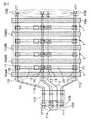
図1は本発明に係るメモリシステムの平面図、図2はメモリシステムの正面図である。
【0030】
同図に示されるメモリシステムは、特に制限されないが、マザーボード101にメモリコントローラ102、コネクタ104A,104B、終端抵抗105、106、信号配線107、電源配線108、終端電圧電源配線109を有し、コネクタ104A,104Bに、例えば前記メモリモジュール1が装着されて構成される。
【0031】
前記信号配線107は、図2に例示されるデータ信号配線112、アドレス・コマンド信号配線113、クロック信号配線117から構成されている。
【0032】
図2に示されるように、一つのメモリモジュール1の同一の面に搭載されているメモリチップ11のメモリアドレス・コマンド入力端子とコマンド・アドレスバッファチップ12のアドレス・コマンド信号出力端子はそれぞれモジュールアドレス・コマンド分配配線19によって接続されており、メモリモジュール1上のメモリチップ11はアドレス・コマンド信号を前記アドレス・コマンドバッファチップ12からモジュールアドレス・コマンド分配配線19を介して受取る。
また、一つのメモリモジュール1の同一の面に搭載されているメモリチップ11のクロック入力端子とアドレス・コマンドバッファチップ12のクロック入力端子とPLLチップ13のクロック出力端子はそれぞれクロック分配配線20によって接続されており、メモリチップ11とアドレス・コマンドバッファチップ12はクロック信号をPLLチップ13からクロック分配配線20を介して受取る。
【0033】
また、図2に示されるように、一つのメモリモジュール1の同一の面に搭載されているメモリチップ11のメモリデータ端子はメモリモジュール1に形成されているモジュールデータ配線15に接続され、コマンド・アドレスバッファチップ12のコマンド・アドレス入力端子はメモリモジュール1に形成されているモジュールコマンド・アドレス配線16に接続され、PLLチップ13のクロック入力端子はメモリモジュール1に形成されているクロック配線17に接続される。
【0034】
図1に例示されるように、複数個のメモリモジュール1はマザーボード101上で平行に配置され、メモリモジュール1は左右のコネクタ104A,104Bによって相互に直列形態で接続される。
【0035】
図1を参照すると、前記コネクタ104A,104Bは、装着された複数のメモリモジュール1のモジュールデータ配線15(モジュールコマンド・アドレス配線16、モジュールクロック配線17)を夫々メモリモジュール1の間で直列的に接続するコネクタ内配線135,133を有し、それらコネクタ内配線135,133はモジュールデータ配線15(モジュールコマンド・アドレス配線16、モジュールクロック配線17)を直列形態に接続する直列経路を構成する。
また、図1及び図2には図示を省略してあるが、モジュール基板には比較的幅広の数種類の電源パターンとしてのモジュール電源配線が形成されている。このモジュール電源配線はコネクタ内電源配線137,138,139に並列的に接続して並列経路を構成する。
【0036】
図2に例示されるように、コネクタ104A,104Bはマザーボード101からメモリモジュール1に電源を供給するための電源配線108を持ち、また隣り合うメモリモジュールの信号端子間を接続する信号配線107(112,113,117)を持っている。前記信号配線107は前記直列経路に接続する第1のシステム配線を構成し、前記電源配線108は前記並列経路に共通接続する第2のシステム配線を構成する。マザーボード上で信号配線107はメモリコントローラ102の下を通り、複数のメモリモジュール11内及びコネクタ104A,104B内に導通し、その両端あるいは少なくとも片側の端には終端抵抗105、106を介して終端電圧電源配線109で所定の電圧VTTに終端されている。
【0037】
図2に示されるように、前記メモリコントローラ102の信号端子はメモリコントローラ102の下を通過する信号配線107にメモリコントローラ102下面側で接続している。図1のように、メモリモジュール1上のメモリチップ11のデータ端子はメモリモジュール1を通過するデータ信号配線112に接続している。なおアドレス・コマンド信号配線113及びクロック信号配線117に対してはメモリコントローラ102側の終端抵抗114は無くてもよい。アドレス・コマンド信号及びクロック信号は一方向にのみ伝播される信号だからである。
メモリモジュール1上のアドレス・コマンドバッファ12のアドレス・コマンド入力端子はメモリモジュール1を通過するアドレス・コマンド信号配線113にそれぞれ接続している。メモリモジュール1上のPLLチップ13のクロック入力端子はメモリモジュール1を通過するクロック信号配線117に接続している。ここでメモリチップ11のデータ端子数をn、メモリモジュール1の片面に搭載されているメモリチップ11の数をmとすると、図1のメモリシステムはm×nのデータ信号配線112を有しており、1回のアクセスにおいてはメモリコントローラ102が発生するコマンド信号のうちのチップセレクト信号により複数のメモリモジュールの内の一つのメモリモジュールの片面に搭載されているm個のメモリチップ11が選択されるようになっている。
【0038】
図3は図1及び図2のメモリシステムの概略的な等価回路図であり、特に1本のデータ信号配線系を示している。このデータ信号配線系を回路的に見ると、主に終端電源109、終端抵抗105,106、マザーボードのデータ信号配線112、コネクタ104Aの内部配線135、コネクタ104Bの内部配線135、メモリモジュール1のモジュールデータ配線15が直列に接続されている。ここでマザーボード101のデータ信号配線112及びメモリモジュールのモジュールデータ配線15の全体の長さは数10mmとなるので、回路的には伝送線として扱われる。そしてマザーボード101のデータ信号配線112の終端抵抗105側の片端にはメモリコントローラ102のメモリコントローラI/O端子128があり、メモリコントローラ102の出力回路123の出力容量及びメモリコントローラ102の入力回路124の入力容量等がメモリコントローラI/O負荷容量125として見えている。また同様に各メモリモジュール1のデータ信号配線15の途中にはメモリチップ11のデータ端子(I/O端子)129があり、メモリチップ11の出力回路120の出力容量及び入力回路121の入力容量等がメモリI/O負荷容量122として見えている。メモリコントローラ出力回路123及びメモリチップ11の出力回路120において回路方式はプッシュプル型、オープンドレイン型などが考えられるがここでは特に問わない。また、特に図示はしないが、例えばスルーレートを制御する機構や、出力インピーダンスを制御する機構があってもよい。このデータ信号配線系において両側が終端抵抗で終端されているのは、メモリコントローラ出力回路123からメモリチップ11の入力回路121へ伝送される信号とメモリチップ11の出力回路120からメモリコントローラ入力回路124へ伝送される信号の両方に対して反射を防ぐ事が目的である。従って、メモリコントローラ102のアドレス出力やコマンド出力のような一方向のみの信号伝達経路に対しては遠端にだけ終端抵抗を配置してよく、前述のように、図1の終端抵抗114は省略しても差し支えない。
【0039】
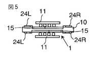
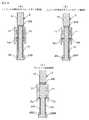
ここで、前記メモリモジュール1の一例を説明する。図4はメモリモジュール1の平面図、図5は側面図である。図4及び図5に示されるメモリモジュール1は、エポキシ樹脂等で成るような概略長方形状のモジュール基板10の表裏に、複数個のメモリチップ11、コマンド・アドレスバッファチップ12、及びPLLチップ13が夫々実装される。
【0040】
メモリモジュール1は、モジュール内の配線として、モジュール基板10の短辺方向に、モジュールデータ配線15、モジュールコマンド・アドレス配線16、モジュールクロック配線17を有し、モジュール基板10の長辺方向に、モジュールコマンド・アドレス分配配線19、及びモジュールクロック分配配線20を有する。モジュールコマンド・アドレス分配配線19及びモジュールクロック分配配線20には終端抵抗22,23が設けられている。終端抵抗22,23はモジュールコマンド・アドレス分配配線19、モジュールクロック分配配線20の末端を終端電源に終端しており、接続されている配線の特性インピーダンスもしくは実効的な特性インピーダンスの抵抗値を有している。それら配線15,16,17,19,20はモジュール基板10の表裏に同等に形成されている。尚、メモリモジュール上のマーク28はメモリモジュール1をコネクタに装着する際、メモリモジュール1の装着方向を指示するものである。
【0041】
メモリモジュール1はモジュール外部端子として、モジュール基板10の対向する長辺部分にモジュールデータ端子対24R,24L、モジュールコマンド・アドレス端子対25R,25L、及びモジュールクロック端子対26R,26Lを有する。それらモジュール外部端子24R,24L,25R,25L,26R,26Lはモジュール基板10の表裏に同等に形成されている。
【0042】
前記モジュールデータ配線15は左右の対応するモジュールデータ端子対24R,24Lを接続する。そしてモジュールデータ配線15の途中に、メモリチップ11のメモリデータ端子Dmが接続される。メモリチップ11は例えば回路基板実装用のバンプ電極をアレイ状に有するフリップチップ(若しくはフリップチップ型半導体集積回路)である。メモリデータ端子Dmは例えばフリップチップの半田バンプ電極とされる。メモリチップ11においてそのようなメモリデータ端子Dmには○印が付されている。
【0043】
前記モジュールコマンド・アドレス配線16は左右の対応するモジュールコマンド・アドレス端子対25R,25Lを接続する。そしてモジュールコマンド・アドレス配線16の途中に、コマンド・アドレスバッファチップ12のバッファコマンド・アドレス入力端子CAiが接続される。例えばコマンド・アドレスバッファチップ12も前記フリップチップであり、前記バッファコマンド・アドレス入力端子CAiは半田バンプ電極とされ、コマンド・アドレスバッファチップ12においてそのようなバッファコマンド・アドレス入力端子CAiは○印が付されている。
【0044】
前記モジュールクロック配線17は左右の対応するモジュールクロック端子対26R,26Lを接続する。そしてモジュールクロック配線17の途中に、PLLチップ13のPLLクロック入力端子CLiが接続される。例えばPLLチップ13はフリップチップであり、PLLクロック入力端子CLiは半田バンプ電極とされ、PLLチップ13においてそのようなPLLクロック入力端子CLiは○印が付されている。
【0045】
前記モジュールコマンド・アドレス分配配線19はモジュール基板10の長辺方向に沿って敷設され、その中間部分が前記コマンド・アドレスバッファチップ12のバッファコマンド・アドレス出力端子CAjに接続される。同様にモジュールクロック分配配線20はモジュール基板10の長辺方向に沿って敷設され、その中間部分がPLLクロック出力端子CLjに接続される。前記バッファコマンド・アドレス出力端子CAj及びPLLクロック出力端子CLjは三角形で示された出力バッファの出力端子が接続されているようにシンボリックに表示されている。
【0046】
前記メモリチップ11のコマンド・アドレス入力用のメモリコマンド・アドレス端子(図示せず)は前記モジュールコマンド・アドレス分配配線19に接続され、また、前記メモリチップ11のクロック入力用のメモリクロック端子(図示せず)及びバッファチップ12のクロック入力用のバッファクロック端子(図示せず)は前記モジュールクロック分配配線20に接続される。メモリチップ11及びバッファチップ12はPLLチップ13からモジュールクロック分配配線20を介して供給されるクロック信号に同期して、メモリ動作及びラッチ動作が可能にされる。
【0047】
なお、図4では前記メモリコマンド・アドレス端子、メモリクロック端子、バッファクロック端子、及びチップ電源端子は明示的に図示していない。また、図4において動作電源用のモジュール電源端子は符号202L,202Rで示される。
【0048】
図6には前記メモリモジュール1におけるメモリチップに関する布線の例が示される。モジュール基板10は、表裏夫々について第1層(表層)及び第2層(内層)の2層配線構造を有し、第1層の配線は実線で示し、第2層の配線は破線で示す。図において○印はメモリチップのバンプ電極のような外部端子、●印は配線層のヴィア(層間孔)である。図のメモリチップはシンクロナスDRAMを一例とするものであり、A0〜A13はアドレス、D0〜15はデータ、CLK,/CLKは2相クロックである。CKEはクロックイネーブル、DML,DMUはデータマスク、/CSはチップ選択、/RASはロウアドレスストローブ、/CASはカラムアドレスストローブ、/WEはライトイネーブル、DQSL,DQSUはデータストローブ、のアクセス制御信号若しくはコマンド信号である。図6に示されるVCCQ,VSSQ,VCC,VSS,VSSQは電源端子である。
【0049】
モジュールコマンド・アドレス分配配線19及びモジュールクロック分配配線20はモジュール基板10上のモジュールデータ配線15に直交する形で布線される。図6より明かなように、それぞれの信号配線19,20はメモリチップ11の対応端子と一筆書き可能な配線経路を介して接続される。この一筆書き配線経路によれば、モジュールコマンド・アドレス分配配線19及びモジュールクロック分配配線20それ自体に分岐のないことは明らかである。
【0050】
不所望な信号反射の抑制という観点からすれば、前記一筆書き経路は最適であるが、全ての配線分岐を否定するものではない。大凡以下の条件を満足すれば不所望な信号反射を生じない。すなわち、D0,D1等のためのモジュールデータ配線15はモジュール基板10の第2層の配線層に形成されており、ヴィア(層間孔)を介してメモリチップ11のメモリデータ端子Dmに接続するとき、ヴィアの部分が僅かに分岐部を形成する。したがって、モジュールデータ配線15は一筆書き可能な第1の配線経路になるがこの第1の配線経路から分岐してメモリデータ端子Dmに接続するヴィアの部分が第2の配線経路を構成することになる。このとき、前記第2の配線経路の配線経路長は、例えば正常動作を保証すべき信号の状態遷移時間に比べて当該信号が前記第2の配線経路を往復する時間の方が短くなるように設定されていればよい。要するは、信号反射の点で無視し得るほど信号経路の短い分岐部分は実質的に一筆書き配線経路の一部と見なし得てもよい。
【0051】
図6のD0,D1のように前記メモリデータ端子を少なくとも隣接する端子相互間でモジュールデータ配線の延在方向にずらして配置すると、メモリデータ端子Dmとモジュールデータ配線15とのコンタクトが形成し易くなる。
【0052】
図7はコネクタ104A,104Bのデータ配線部分を概略的に示す縦断面図である。コネクタ104Aは一方の側面に1条の水平溝を有し、この水平溝の内面の上面及び下面にコネクタ端子列130が形成されている。コネクタ端子列130はコネクタ端子毎にコネクタ内配線135を介してデータ信号配線112の対応配線に接続される。コネクタ104Bは両側面に夫々1条の水平溝を有し、この水平溝の内面の上面及び下面にコネクタ端子列131,132が形成されている。ここのコネクタ端子列131の端子とコネクタ端子列132の端子とは対応端子同士がコネクタ内配線133,134によって直列に接続されている。
【0053】
図8はコネクタ104A,104Bの電源配線部分を概略的に示す縦断面図である。マザーボード101には電源配線108が設けられ、前記電源配線108には、コネクタ端子列130に含まれる電源コネクタ端子がコネクタ内配線137を介して接続され、コネクタ端子列131に含まれる電源コネクタ端子がコネクタ内配線138を介して接続され、コネクタ端子列132に含まれる電源コネクタ端子がコネクタ内配線139を介して接続される。電源に関しても図7の接続を採用する事は可能であるが、図8の接続形態を採用した方がメモリチップ11などに対する電源供給が安定化する。前記コマンド・アドレス配線113に関しても電源配線136と同じようにコネクタ104A,104Bのコネクタ端子列130,131,132に接続してもよい。
【0054】
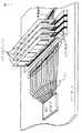
図9はコネクタ104A,104Bに上記メモリモジュール1を装着する際の斜視図である。前記コネクタ104A,104Bに上記メモリモジュール1を装着するには、図9のように、メモリモジュール1の端子列がコネクタ104A,104Bの端子列130,131に挿入するように差し込む。このときコネクタのマーク140はメモリモジュール1の面の向きや方向を指示するためのもので、メモリモジュール1の装着方向指示マーク28とコネクタのマーク140が最も近づくようにメモリモジュール1の面と方向を合わせる。
【0055】
図10はコネクタ104A,104Bに上記メモリモジュール1を装着した時の断面図である。図10では便宜上、メモリモジュール1の上側のメモリチップに接続する経路を信号経路とし、メモリモジュール1の下側のメモリチップに接続する経路を電源経路としている。データ信号経路はコネクタ104A,104B及びメモリモジュール1を分岐せずに通過する配線経路とされる。また各メモリモジュール1の電源配線もマザーボード101の電源配線108とそれぞれ装着されているコネクタ104A,104Bを介して接続されるので、十分な電力供給を実現でき、電源の電圧降下を防止する事ができる。
【0056】
上記第1のメモリシステムによれば以下の作用効果を得ることができる。図1及び図2より明らかなように、メモリモジュール1上のモジュールデータ配線15は、マザーボード101上のデータ信号配線112と共にメモリアクセスデータバスを構成するから、複数個のメモリモジュール1を直列させたメモリシステムでは、各メモリモジュール1のモジュールデータ配線15が一連に接続され、個々のモジュールデータ配線15は、メモリシステムのマザーボード101上のデータ信号配線112に対する分岐配線を構成しない。したがって、メモリシステムのマザーボード101上のデータ信号配線112に対する分岐に起因するような信号反射を生じない。例えば、図11及び図12のSSTLインタフェースを有する比較例に係るメモリシステムの場合には、マザーボード上のバスに対してメモリモジュールは分岐接続されているから、各分岐毎にスタブ抵抗を配置して不所望な信号反射に対処しようとしている。このため比較例ではマザーボード上のバス信号の振幅が小さくなって安定動作が妨げられてしまう。図1及び図2のメモリシステムではマザーボード上の信号配線の不所望な負荷は大きくならず、信号反射を阻止する構成が信号振幅の低下を妨げることはない。
【0057】
更に、個々のメモリモジュール1上において、メモリチップ11のデータ端子Dmは直接前記モジュールデータ配線15に接続するから、モジュールデータ配線15に対する分岐に起因するような信号反射も生じない。
【0058】
そして、メモリモジュール1は、メモリアクセスデータバスのバス幅に応じたビット数の並列アクセスが保証されている。これにより、アクセス時間の増大を抑制しながら、信号反射による信号波形の乱れを抑えて信号伝送の信頼性を向上させることが可能になる。図13及び図14に示される比較例の場合にはメモリモジュール上で複数のメモリチップはモジュール内データバスを共有し、メモリモジュールはシリアルバスに直列的に接続され、当該メモリモジュールはシリアルバスに分岐接続されていないから分岐に起因する信号反射は実質的に生じないが、バスが長くなって配線遅延が増大するために、高速アクセスには限界がある。
【0059】
電源などは前記コネクタ内配線137,138,139から成る並列経路を介してマザーボード101から各メモリモジュール1に並列的に供給されるから、電源やクロックの供給が安定化する。例えば電源をメモリモジュールに直列的に供給すると、途中で一つのメモリモジュールが電源ノイズを生ずるとその影響が後段に伝播する虞がある。並列経路から動作電源を並列に供給する場合にはそのような虞はなく、メモリ動作に高い信頼性を保証することが可能になる。
【0060】
モジュールデータ端子対24L、24Rやモジュールデータ配線15の態様として、前記複数のメモリチップ11がモジュール基板10の長手方向に沿って配列されるとき、前記モジュールデータ端子対24L,24Rはモジュール基板10のメモリチップ搭載面における一方の長辺部分と他方の長辺部分とに配置する。換言すると、前記モジュールデータ配線15を、モジュール基板10のメモリチップ搭載面における一方の長辺部分から他方の長辺部分に向けて延在させる。
これにより、モジュールデータ配線15の配線長は必然的に短くなり、配線の寄生容量や配線抵抗が小さくなる。
【0061】
モジュールデータ配線15をモジュール基板10の短辺方向に直線状に敷設し、モジュールコマンド・アドレス配線16,20を概略十文字に敷設するから、モジュールデータ配線と共にモジュールコマンド・アドレス配線の配線長短縮に最適である。
【0062】
また、モジュールアドレス端子対25R、25Lを結合する前記モジュールコマンド・アドレス配線16は、コマンド・アドレスバッファチップ12を介してコマンド・アドレス分配配線19と分離されているから、モジュールコマンド・アドレス配線16上に無視し得ないインピーダンス不整合点が形成されることも阻止可能である。
【0063】
前記モジュールコマンド・アドレス分配配線19配線に対しては、その特性インピーダンスを有する抵抗素子22,23で終端することによって、モジュールコマンド・アドレス配線19の端が整合終端され、当該配線19において信号反射による波形の乱れを極力抑えることが可能になる。
【0064】
ここで、図1及び図2のメモリシステムにおけるデータ信号波形のシミュレーション結果を説明する。
【0065】
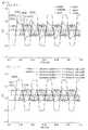
先ず、比較例として、図15には図11の形式のメモリシステムにおけるSSTLのシミュレーション回路が示される。図16の(A)には図15のシミュレーション回路におけるライト時のSSTL信号波形シミュレーションの結果が示される。図16の(B)には図15のシミュレーション回路におけるリード時のSSTL信号波形シミュレーションの結果が示される。図11のような回路形式のSSTLでは高速動作や分岐配線が長い場合には受信端の信号波形に乱れが生じる場合がある。
【0066】
図17には図2で説明したようなメモリシステムのデータ信号に関するシミュレーション回路が例示される。ここで、ライト動作シミュレーションの時、ドライバ2010はメモリコントローラ102にあり、リード動作シミュレーションの場合は各メモリモジュールにあるとする。ドライバ2010は出力抵抗2009を有するプッシュプル型出力回路を想定している。ここでは出力抵抗を50Ωとしている。また終端抵抗Rtはデータ信号配線の実効的特性インピーダンスとほぼ同じ値にしている。メモリコントローラ側の終端抵抗55Ωはメモリコントローラと近端メモリモジュールの間の伝送線の特性インピーダンスとほぼ同じ値にしている。
【0067】
図18の(A)は図17のシミュレーション回路(図2で説明したメモリシステム)におけるライト動作のシミュレーション結果である。メモリチップに入力されるデータ信号bQR0〜3(2001〜2004)を見ると、比較例である図16の(A)に示されるライト動作のシミュレーション結果におけるメモリチップに入力されるデータ信号bQR0〜3(2101〜2104)と比べて波形の乱れが小さい事がわかる。図18の(B)は図17のシミュレーション回路(図2で説明したメモリシステム)におけるリード動作のシミュレーション結果である。図中DQRSIN1〜DQRSIN4は夫々メモリチップのデータ信号bQR0〜3(2001〜2004)を出力させた時にそれぞれメモリコントローラに入力されるデータ信号DQRSIN1〜4(2006)である。図16の(B)の比較例に係るメモリシステムのリード動作のシミュレーション結果におけるメモリチップで入力されるデータ信号DQRSIN1〜4(2106)と比べると、波形の乱れが小さい事がわかる。出力抵抗を15Ωにした系においても同様に良好な波形が得られる。この場合には消費電力は増えるが論理振幅を大きくできる効果がある。
【0068】
《第2乃至第5のメモリシステム》
図19は本発明による第2のメモリシステムにおけるデータ信号配線系の等価回路図である。本メモリシステムでは図3の第1のメモリシステムと比較すると、メモリコントローラ102側の終端抵抗105に第1のスイッチ230が、またメモリコントローラ102と逆側の終端抵抗106に第2のスイッチ231が新しく追加されている。このうち第1のスイッチ230をメモリのリード(読み出し)時にオン、そしてメモリのライト(書き込み)時にオフとすることにより、メモリのリード(読み出し)時に信号配線112のメモリコントローラ102側の終端をインピーダンス整合させる事ができる。また第2のスイッチ231をメモリのライト(書き込み)時にオン、メモリのリード(読み出し)時にオフとすることにより、メモリのライト(書き込み)時にメモリコントローラ102から最遠端の信号配線135につながる終端をインピーダンス整合させる事ができる。
【0069】
第1のスイッチ230及び第2のスイッチ231は、例えばMOSトランジスタから成るようスイッチ素子で実現でき、その制御はメモリコントローラ102がアクセス動作に応じて制御すればよい。またコマンド・アドレスバッファチップ12にそのスイッチ制御機能を持たせてもよい。
【0070】
上記図3の第1のメモリシステムでは信号配線112及びコネクタ内配線135等から成る直列配線経路の両端の終端が常に抵抗終端されており、メモリのライト(書き込み)時とメモリのリード(読み出し)時において両方の抵抗に電流が流れ、消費電力が大きくなる。図19の第2のメモリシステムでは信号配線112及びコネクタ内配線135等から成る直列配線経路の両端の終端のうち、メモリのライト(書き込み)時とメモリのリード(読み出し)時に応じて一方だけが抵抗終端され、一方の終端抵抗にしか電流が流れないので、第1のメモリシステムに比べて低消費電力を図ることができる。また論理振幅を大きくできるのでノイズマージンを大きくする事も可能である。
【0071】
図20は本発明による第3のメモリシステムにおけるデータ信号配線系の等価回路図である。同図に示されるメモリシステムは、図3の第1のメモリシステムに対して、メモリコントローラ102側の終端抵抗105にスイッチ230を追加した点が相違される。スイッチ230をメモリのリード(読み出し)時にオン、メモリのライト(書き込み)時にオフとすることにより、メモリのリード(読み出し)時に信号配線112のメモリコントローラ102側の終端をインピーダンス整合させる事ができる。なおスイッチ230はMOSトランジスタで実現でき、その制御はメモリコントローラ102で行えばよい。上記第1のメモリシステムでは信号配線112の両端の終端が常に抵抗終端されており、メモリのライト時とメモリのリード時において両方の抵抗に電流が流れ、消費電力が大きくなる。これに対し、第3のメモリシステムでは信号配線112の両端の終端のうち、メモリのライト時にはメモリコントローラ102と逆側の終端のみ抵抗106で終端され、一方しか電流が流れないので、第1のメモリシステムに比べて低消費電力化できる。またライト時のノイズマージンを大きくすることも可能に成る。また第2のメモリシステムでは信号配線112及びコネクタ内配線133,135の直列経路の両端に2つのスイッチが必要となり製造コストが大きくなる。
この点において、第3のメモリシステムではスイッチは1つとなり、第2のメモリシステムに比べて低コスト化できる。
【0072】
図21は本発明による第4のメモリシステムにおけるデータ信号配線系の等価回路図である。本メモリシステムでは図3の第1のメモリシステムに対し、メモリコントローラ102側の終端抵抗105が取り除かれ、更に、メモリチップ11の出力回路としてオープンドレイン型の出力トランジスタ233を採用する。
プッシュプル型出力回路は動作時においてトランジスタの出力抵抗が変動するので、信号配線112等からなるデータ用の直列配線経路の実効的な特性インピーダンスを乱し、反射が起き易くなる。これに対し、オープンドレイン型出力トランジスタ233によって構成されるオープンドレイン出力回路を採用すれば、動作時の出力抵抗を高くほぼ一定にできるので、動作時において前記データ用直列配線経路の実効的な特性インピーダンスを乱さない。この理由により、本メモリシステムではメモリコントローラ102と逆側の終端のみを抵抗106でインピーダンス整合している。これにより終端抵抗は一つとなるので,第1のメモリシステムに比べて低コスト化かつ低消費電力化できる。
【0073】
図22には第4のメモリシステムにおけるコマンド・アドレス信号配線系に関する等価回路図である。コマンド・アドレス信号配線系では信号はメモリコントローラ102からコマンド・アドレスバッファチップ12へ向かって一方向にのみ伝送されるので、他の例と同様に終端抵抗はメモリコントローラ102と逆側の終端の抵抗106のみで構わない。
【0074】
図23は本発明による第5のメモリシステムにおけるデータ信号配線系の等価回路図である。同図に示されるメモリシステムでは前記第1のメモリシステムに対し、図21の第4のメモリシステムとは逆にメモリコントローラ102と逆側の終端抵抗106が取り除かれ、メモリコントローラ102の出力回路にオープンドレイン型出力回路を構成するオープンドレイン出力トランジスタ235を採用する。これにより図21の第4のメモリシステムと同様の理由により、 第1のメモリシステムに比べて低コスト化かつ低消費電力化が可能になる。
【0075】
《メモリコントローラ》
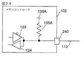
図24は本発明による第1のメモリシステム(図3参照)に最適なメモリコントローラ102の回路図である。同図に示されるメモリコントローラ102はデータ信号配線112の実効的な特性インピーダンスと整合する抵抗105Aを内蔵しており、データ信号端子240とメモリコントローラ内部の終端電源109Aに接続されている。同図に示される構成を採用したメモリコントローラ102を第1のメモリシステムに用いる事により、図1に示したマザーボード101のメモリコントローラ102側の外付け終端抵抗105が不要となり、低コスト化できる。
【0076】
図25は本発明による第2のメモリシステム(図19参照)に最適なメモリコントローラ102の回路図である。同図に示されるメモリコントローラ102は第1のスイッチ切り替え信号端子241及び第2のスイッチ切り替え信号端子241を有しており、それぞれメモリコントローラ102の外部に設けられた第1のスイッチ243及び第2のスイッチ244のオン・オフを切り替える信号を出力する。これらの信号端子241,242の出力はメモリコントローラ102の入力モード信号245を出力回路246が第1のスイッチ切り替え信号端子241へ出力し、またメモリコントローラの入力モード信号245を反転出力回路247が第2のスイッチ切り替え信号端子242へ反転出力する事によって出力される。ここでメモリコントローラ102の入力モード信号245は、データ入力時にレベル“H”、データ出力時にレベル“L”にされる。また、メモリコントローラ102の外部に設けられた第1のスイッチ243及び第2のスイッチ244は例えば、MOSトランジスタで構成され、ゲートレベル“H”でオン、ゲートレベル“L”でオフにされる。本メモリコントローラ102を第2のメモリシステムに用いる事により、前述のように、不要な終端抵抗による電力消費を抑えることが可能になる。終端抵抗105は図24のようにメモリコントローラ102に内蔵してもよい。
【0077】
図26は本発明による第3のメモリシステム(図20参照)に最適なメモリコントローラ102の回路図である。同図に示されるメモリコントローラ102は、図24の第1のメモリシステムにおけるメモリコントローラに対して内蔵終端抵抗105Aの信号端子240への接続を制御するスイッチ250が内蔵されている。このスイッチ250はメモリコントローラ102の入力モード信号245でオン・オフされる。これによって終端抵抗105Aはそれが必要となるタイミング、即ちメモリコントローラ102の入力時のみ有効となる。これにより、図26のメモリコントローラ102の構成を第3のメモリシステムに採用する事により、不要な終端抵抗による電力消費が抑えられ、低消費電力のメモリシステムを提供する事が可能となる。メモリコントローラ102側のマザーボード101上に終端抵抗105を設置する必要がないので低コスト化できる。
【0078】
図27には本発明による第3のメモリシステム(図20参照)に最適なメモリコントローラ102の更に別の回路例を示す。同図に示されるメモリコントローラ102は、図25の第2のメモリシステムにおけるメモリコントローラの反転出力回路247及びスイッチ切り替え信号端子242が取り除かれたものである。図27の構成を第3のメモリシステムのメモリコントローラ102に採用することにより、不要な終端抵抗による電力消費が抑えられ、低消費電力のメモリシステムを提供する事が可能となる。
【0079】
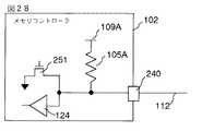
図28は本発明による図23の第5のメモリシステムに最適なメモリコントローラの回路図である。同図に示されるメモリコントローラ102は図24の第1のメモリシステムにおけるメモリコントローラ102の出力回路にオープンドレイン型出力回路を構成するオープンドレイントランジスタ251を用いたものである。構成を本発明の第5のメモリシステムのメモリコントローラ102に採用する事により、マザーボード101のメモリコントローラ側の終端抵抗105が不要となり、低コスト化できる。もちろん図1に示したように終端抵抗(105)をメモリコントローラの外側に設置すしても良い。
【0080】
《その他のメモリモシステムの例》
図29には図4とは異なった構造の第2のメモリモジュールの断面が示される。図29の(A)は1バンク形式のメモリモジュールにおけるデータ信号配線に関する断面図である。本メモリモジュール2においてモジュールデータ端子対24L,24Rはモジュール基板10の一方の長辺部分に沿って両面に配置される。モジュールデータ配線15は貫通孔200を介してモジュールデータ端子対24R,24Lを接続している。モジュールデータ配線15は図4の第1のメモリモジュール1と同じように一筆書きの配線経路をもち、モジュールデータ配線15とメモリチップ11のチップデータ端子Dmとの間には前記ヴィア(層間孔)によって形成されるような実質的に無視し得るほど小さな分岐を生じている。この分岐部分は前述より明らかな如く不所望な信号反射の要因にはならない。
【0081】
図29の(B)は2バンク形式のメモリモジュールの場合における信号配線に関する断面図である。図29の(A)のメモリモジュール2では1本のモジュールデータ配線15はモジュール10の片面に設置されている一つのメモリチップ11のメモリデータ端子Dmに接続されているのに対し、図29の(B)のメモリモジュールでは、1本のモジュールデータ配線15はモジュール基板10の両面に設置されているメモリチップ11,11のメモリデータ端子Dm,Dmに一筆書き接続されている。
【0082】
図29の(C)はメモリモジュール2の電源配線に関する断面図である。モジュール電源配線201は、メモリチップ11のチップ電源端子Dpに配線されているが、一筆書き配線経路で接続する必要はなく、モジュール電源端子202L、202Rから夫々分岐する如く延在されている。なおモジュールコマンド・アドレス配線16やモジュールクロック配線17はモジュール電源配線201と同様に扱ってもよいし、図4のようにモジュールデータ配線15と同様に扱ってもよい。
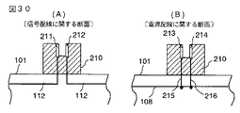
【0083】
図30の(A)は第2のメモリモジュール2のためのコネクタ210を信号配線に着目して示す。コネクタ210は一条の垂直溝を有し、垂直溝の左右内面にコネクタ端子列が紙面の表裏方向に形成され、図では代表してコネクタ端子211,212が示されている。マザーボード上のデータ信号配線112はコネクタ端子211、212に接続され、そこでで分断されている。
【0084】
図30の(B)は第2のメモリモジュール2のためのコネクタ210を電源配線に着目して示す。電源用のコネクタ端子として代表的に示されたコネクタ端子213,214は、電源配線108から分岐された分岐配線215,216に夫々接続されており、電源配線108は途中で電気的に分断されていない。
【0085】
図31の(A)にはメモリモジュール2を装着したメモリシステムの断面が信号配線に関して示される。同図に示されるメモリシステムにおいて、メモリモジュール2がコネクタ210に装着されると、コネクタ210で分断されたデータ信号配線112が、メモリモジュール2のモジュールデータ配線15を介して繋がる。
【0086】
図31の(B)にはメモリモジュール2を装着したメモリシステムの断面が電源配線に関して示される。本メモリシステムにおいてはメモリモジュール2がコネクタ210に装着されると、メモリモジュール2のモジュール電源端子がコネクタ210の電源コネクタ端子213,214を介してマザーボード101の電源配線108に接続する。尚、前記コマンド・アドレス信号配線113は、図30の(B)の電源配線108と同じように、マザーボード101のコマンド・アドレス信号線113からコネクタ210を介してメモリモジュール2に接続してもよいし、もちろん図31の(B)のように接続してもよい。
【0087】
第2のメモリモジュール2によっても、上記同様に、不所望な信号反射の原因になる分岐を作らず、配線長の増大を招くことなく、マザーボード101のデータ信号配線にメモリチップを電気的に接続させることがができる。
【0088】
図32は第3のメモリモジュールの平面図である。同図に示されるメモリモジュール3において、モジュールデータ端子対24L,24Rはモジュール基板10の同じ面の同じ辺で隣り合うように配置され、当該端子対24L,24Rは往復的に敷設されたモジュールデータ配線15によって結合され、そのモジュールデータ配線15の途中で一つのメモリチップ11のメモリデータ端子Dmに一筆書き接続されている。
【0089】
図33は第3のメモリモジュール3をコネクタで接続する形態を例示する。図33の(A)は図32のモジュールデータ端子24Lの位置での縦断面を想定し、図33の(B)は図32のモジュールデータ端子24Rの位置での縦断面を想定している。図33の(A)においてデータ信号配線112はマザーボード101からコネクタ300のデータコネクタ端子301L及びモジュールデータ端子24Lを介してメモリモジュール3のモジュールデータ配線15に接続される。
前記モジュールデータ配線15はモジュール基板10上で経路が折り返され、図33の(B)に例示されるように、その隣のモジュールデータ端子24Rに至り、コネクタ300のデータコネクタ端子301Rからマザーボード101のデータ信号配線112に導通する。マザーボード101上の電源配線108との接続態様については特に図示はしないが、図31の(B)と同様に、マザーボード101の電源配線108からコネクタを介してメモリモジュール3のモジュール電源端子に接続すればよい。
【0090】
第3のメモリモジュール3によっても、上記同様に、分岐を作ることなくまた配線長の増大を招くことなくデータ信号配線にメモリチップを接続する事ができる。
【0091】
《ダミーメモリモジュール》
メモリシステムを構成するメモリモジュールの一部を置き換え可能なダミーメモリモジュールについて説明する。
【0092】
図34には図4で説明した第1のメモリモジュール1と共に利用してメモリシステムを構成可能なダミーメモリモジュール1Aの平面図、図35にはダミーメモリモジュールの側面図が示される。同図に示されるダミーメモリモジュール1Aは図4のメモリモジュール1に対してメモリチップ11、コマンド・アドレスバッファチップ12、PLLチップ13、モジュールコマンド・アドレス分配配線19、モジュールクロック分配配線20、終端抵抗22,23を省略した構成を備える。換言すれば、ダミーメモリモジュール1Aは、モジュール基板10に、24L、25Rで代表されるモジュール端子対、モジュールデータ配線15、モジュールコマンド・アドレス配線16、及びモジュールクロック配線17を有する。図34に示されるダミーメモリモジュール1Aは図1及び図2で説明したメモリシステムにおいて、メモリモジュール1の代わりにコネクタ104A,104Bに装着して利用すれば、信号線112,113,117の経路に分岐を作ることなくまた配線長の増大を招くことなく、メモリシステムのメモリ容量を変更することが可能になる。
【0093】
特に図示はしないが、ダミーメモリモジュール1A上の配線15,16,17にチップ11,12,13の入力容量を再現したダミー容量を設ければ、実効的特性インピーダンスを乱さず、波形の乱れを更に抑える事が可能になる。
【0094】
図36は第2のメモリモジュール2と共に利用可能なダミーメモリモジュール2Aを示し、(A)はa−a断面図、(B)は拡大表面図、(C)は拡大裏面図である。図36のダミーメモリモジュール2Aは、図29に示されるメモリモジュール2に対してメモリチップ11等のデバイスが搭載されていない構成を有する。要するに、モジュール基板10の表裏に24L,25Rで代表されるモジュール端子対、15で代表されるモジュール配線、モジュール配線の貫通孔200によって構成されている。図31のメモリシステムにおいてメモリモジュール2の代わりに前記ダミーメモリモジュール2Aを用いれば、分岐を作ることなく、また配線長の増大を招くことなく、メモリシステムのメモリ容量を変更する事が可能になる。
【0095】
図37には第3のメモリモジュール3と共に利用可能なダミーメモリモジュール3Aが示される。同図に示されるメモリモジュール3Aは、図32に示されるメモリモジュール3に対してメモリチップ11等のデバイスが搭載されていない構成を有する。要するに、モジュール基板10の表面に24L,25Rで代表されるモジュール端子対、15で代表されるモジュール配線が設けられて構成されている。第3のメモリモジュール3の代わりにダミーメモリモジュール3Aを用いれば、分岐を作ることなく、また配線長の増大を招くことなく、メモリシステムのメモリ容量を変更する事が可能になる。
【0096】
《終端用メモリモジュール》
メモリシステムのマザーボードに外付けされる終端抵抗を搭載した終端用のメモリモジュールを説明する。
【0097】
図38は第1のメモリモジュール1に終端抵抗を搭載して成る終端用のメモリモジュール1Bを示し、(A)は部分平面図、(B)は側面図である。図38に示されるメモリモジュール1Bは、図1のモジュール端子対24L,24R等の一方のモジュール端子24R等を取り除き、残りのモジュール端子24Lなどに接続されたモジュールデータ配線15などに終端抵抗106Aを接続し、この終端抵抗106Aに終端電源端子30を接続して構成される。図38の(B)に示されるようにモジュール基板10の裏面側も同様に構成される。
【0098】
図39は図34のダミーメモリモジュール1Aに対応される終端用のダミーメモリモジュール1Cを示す。図34のダミーメモリモジュールに対してモジュール端子対24L,24R等の一方のモジュール端子24R等を取り除き、残りのモジュール端子24Lなどに接続されたモジュールデータ配線15などに終端抵抗106Aを接続し、この終端抵抗106Aに終端電源端子30を接続して構成される。
【0099】
図1のメモリシステムにおいて前記メモリモジュール1の代わりに図38に示されるメモリモジュール1B又は図39に示されるメモリモジュール1Cを用いれば、マザーボード101上の終端抵抗106を使うことなく、マザーボード101上の信号配線112、113、117をメモリモジュール上で終端できる。
【0100】
図40は図29の(A)に示されるメモリモジュール2に終端抵抗を搭載して成る終端用のメモリモジュール2Bを示し、(A)はa−a断面図、(B)は拡大表面図、(C)は拡大裏面図である。図40に示されるメモリモジュール2Bは、図29のモジュール端子対24L,24R等の一方のモジュール端子24R等を取り除き、残りのモジュール端子24Lなどに接続されたモジュールデータ配線15などに終端抵抗106Aを接続し、この終端抵抗106Aに終端電源端子30を接続して構成される。
【0101】
図31のメモリシステムにおいてメモリモジュール2の代わりに前記終端用メモリモジュール2Bを利用すれば、マザーボード101上の終端抵抗106を使うことなく、信号配線112をメモリモジュール上で終端する事が可能となる。
別の信号配線113,117についても同様の構成を採用する事が可能である。
【0102】
図41は図32に示されるメモリモジュール3に終端抵抗を搭載して成る終端用のメモリモジュール3Bを示す。図41に示されるメモリモジュール3Bは、図32のモジュール端子対24L,24R等の一方のモジュール端子24R等を取り除き、残りのモジュール端子24Lなどに接続されたモジュールデータ配線15などに終端抵抗106Aを接続し、この終端抵抗106Aに終端電源端子30を接続して構成される。図32に示されるメモリモジュール3の代わりに前記終端用メモリモジュール3Bを利用すれば、マザーボード101上の終端抵抗106を使うことなく、信号配線112などをメモリモジュール上で終端する事が可能となる。
【0103】
《コネクタのその他の形態》
メモリシステムを構成するコネクタのその他の形態について説明する。
【0104】
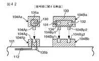
図42及び図43には図7及び図8の前記コネクタ104A,104Bの別の形態が例示される。図42はデータ信号線112に接続する部分を断面で示し、図43は電源線108に接続する部分を断面で示す。コマンド、アドレス信号線113、クロック信号線117に接続する部分は例えば図43のように構成される。
【0105】
要するに、図42、図43の構成は図7、図8のコネクタ104A,104Bを上下2分割で着脱可能に構成して、メモリモジュール1、1A,1Bの装着を容易化したものである。
【0106】
即ち、コネクタ104Aを104Aaと104Abに2分割し、分割片104Aaの底面には凸条に形成された1条のコネクタ端子部104Apが設けられ、分割片104Abの上面には凹条に形成された1条のコネクタ端子部104Agが設けられる。同様に、分割片104Baの底面には凸条に形成された2条のコネクタ端子部104Bp1,104Bp2が設けられ、分割片104Bbの上面には凹条に形成された2条のコネクタ端子部104Bb1,104Bg2が設けられる。
【0107】
図42において、前記コネクタ端子部104Ap、104Agのデータ信号線112に対応する部分では、コネクタ内蔵配線135a,135bによってデータ信号配線112がコネクタ端子列130の対応端子に導通可能にされる。また、図43において、前記コネクタ端子部104Ap、104Agの電源配線108に対応する部分ではコネクタ内蔵配線137a,137bによって電源配線108がコネクタ端子列130の対応端子に導通可能にされる。コマンド・アドレス信号配線113、クロック信号線117に接続するコネクタ104Aa,104Abの部分も図43の場合と同様にされる。
【0108】
更に、図42に示されるようにコネクタ104Bの分割片104Baにおけるコネクタ端子列131と132のデータ信号線112に対応する対応端子はコネクタ内蔵配線133,134によって相互に導通され、実質的に図7と同様に構成される。また、図43において、前記コネクタ端子部104Bp1、104Bg1の電源配線108に対応する部分ではコネクタ内蔵配線138a,138bによって電源配線108がコネクタ端子列131の対応端子に導通可能にされる。同様に、前記コネクタ端子部104Bp2、104Bg2の電源配線108に対応する部分ではコネクタ内蔵配線139a,139bによって電源配線108がコネクタ端子列132の対応端子に導通可能にされる。コマンド・アドレス信号配線113、クロック信号線117に接続するコネクタ104Ba,104Bbの部分も図43の場合と同様にされる。
【0109】
図42及び図43のコネクタを用いたメモリシステムにメモリモジュールを装着する作業は次の通りである。例えば、メモリモジュール1の左右のモジュール端子にコネクタ分割片104Aaのコネクタ端子列130とコネクタ分割片104Baのコネクタ端子列131を結合する。続けて次のメモリモジュール1の左右のモジュール端子にコネクタ分割片104Baのコネクタ端子列132とコネクタ分割片104Baのコネクタ端子列131を結合する。このようにして、必要な数のメモリモジュールを横に直列に結合した後、メモリモジュールに結合されたコネクタ分割片104Aaのコネクタ端子104Apを対応するコネクタ分割片104Abのコネクタ端子104Agに結合すると共に、メモリモジュールに結合されたコネクタ分割片104Baのコネクタ端子104Bp1,104Bp2を対応するコネクタ分割片104Bbのコネクタ端子104Bg1,104Bg2に結合する。これにより、メモリモジュールの設置作業に必要となる空間がメモリシステムの上方空間のみとなるので、メモリシステムの周囲に他の装置を設置したり、メモリシステムを壁で囲まれた場所に設置する事ができる。
【0110】
図44にはコネクタの機能を一部備えたメモリモジュールの例が示される。同図に示されるメモリモジュール1Cは、図4のメモリモジュール1に、図43のコネクタ端子列132に相当する機能を持つコネクタ端子列132Eと前記コネクタ端子部104Bp2に相当する機能を持つコネクタ端子部104BpEとを付加して構成される。コネクタ端子列132Eはモジュールデータ配線15に接続され、コネクタ端子部104BpEはモジュール電源配線、モジュールコマンド・アドレス配線16、及びモジュールクロック配線17に接続される。前記コネクタ端子部104BpEに対応してマザーボード101にはコネクタ104Bが配置される。図44の構成を採用することにより、メモリモジュール設置作業において図42及び図43の構成に比べてメモリモジュールをマザーボードに接続する作業量を低減できる。更にメモリシステムの部品点数も削減でき、メモリシステムの低コスト化に寄与することも可能であると考えられる。
【0111】
図45はメモリモジュール1に適用可能な別の形態のコネクタをデータ信号線112に接続する部分の断面で示す。コネクタ154,155,156は、夫々上向きの凹溝に形成されたコネクタ端子154A,155A,156Aを有し、メモリモジュール1を起立させて支持することができる。コネクタ157は下向きの凹溝に形成されたコネクタ端子157A,157Bを有し、起立された一対のメモリモジュール1に挿入される。マザーボード101上データ信号配線112は、コネクタ内配線154a,154bを介してコネクタ端子154Aに、コネクタ内配線155a,155bを介してコネクタ端子155Aに、コネクタ内配線156a,156bを介してコネクタ端子156Aに、コネクタ内配線157a,157bを介してコネクタ端子157A、157Bに、夫々結合する。したがって、コネクタ154,155,157にメモリモジュール1を装着すると、配線154a,157a,156aが夫々データ信号線112に導通し、配線154b,157b,156bが夫々データ信号線112に導通する。メモリモジュール1は分岐を有すること無くデータ信号配線112に導通可能になる。
【0112】
図46はメモリモジュール1に適用可能な更に別の形態のコネクタをデータ信号線112に接続する部分の断面で示す。コネクタ164は上向きの凹溝に形成されたコネクタ端子164Aを有し、コネクタ165は上向きの凹溝に形成されたコネクタ端子165A,165Bを有し、メモリモジュール1を起立させて支持することができる。コネクタ166は下向きの凹溝に形成されたコネクタ端子166A,166Bを有し、起立された一対のメモリモジュール1に挿入される。マザーボード101上のデータ信号配線112は、コネクタ内配線164a,164bを介してコネクタ端子164Aに接続する。コネクタ端子165Aと165Bはコネクタ内配線165a,165bを介して相互に結合する。コネクタ端子166Aと166Bはコネクタ内配線166a,166bを介して相互に結合する。したがって、コネクタ164,165,167にメモリモジュール1を装着すると、配線164a,166a,165aが夫々データ信号線112に導通し、配線164b,166b,165bが夫々データ信号線112に導通する。メモリモジュール1は分岐を有すること無くデータ信号配線112に導通可能になる。
【0113】
図47は図46のコネクタにおける電源配線部分の断面を示す。マザーボード101上の電源配線108は、途中で分岐してコネクタ内配線164c、165cを介して対応するコネクタ端子164A、165Aの電源用端子に接続する。
【0114】
図48には図46及び図47のコネクタにメモリモジュールを搭載した状態が示される。このコネクタ164〜166を用いれば、分岐を作ることなく、また配線長の増大を招くことなく、データ信号配線にメモリ素子を接続するメモリシステムをマザーボード上に小占有面積で形成できる。図45のコネクタ154〜157を用いても同じである。また、コマンド・アドレス信号配線113、クロック信号配線117の接続に関しても図45又は図46のコネクタを用いればよい。
【0115】
《メモリシステムのその他の形態》
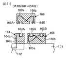
図49の(A)斜視図、(B)側面図にはメモリモジュールの更に別の形態が示される。同図に示されるメモリモジュール1Cは前記メモリモジュール1に対して、データ端子対24L,24Rに代表されるモジュール端子対170L,170Rがモジュール基板10に対して直交する向きに形成されている点が相異される。
【0116】
図50には図49のメモリモジュールを搭載したメモリシステムの一例が示される。マザーボード101上のコネクタとして、特に制限されないが、図46のコネクタ164、165が用いられている。図45のコネクタ154、155、156などを用いてもよい。図46のコネクタ166、図45のコネクタ157などが不用になり、また、メモリモジュールの設置作業に必要となる空間がメモリシステムの上方のみとなるので、メモリシステムの周囲に他の装置を設置したり、メモリシステムを壁で囲まれた場所に設置する事ができる。
【0117】
図51には図1のメモリシステムをコネクタ、メモリモジュールを使わずに一つの基板260に形成した例が示される。これにより、メモリシステムを小型化でき、データアクセス時間も短縮できる。部品点数が削減され、低コスト化に寄与する。さらに、図52に例示されるように、メモリシステムを同一基板260上の両面に形成してもよい。これにより、小型化と同時にメモリ容量を拡大できる。
【0118】
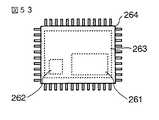
また、図53に例示されるように、図52のメモリシステム261をCPU262と一緒に基板263に実装し、全体をパッケージ264で封止し、MCM(マルチチップモジュール)を構成してもよい。前記CPU262は、メモリモジュール261のメモリコントローラ102に接続され、このメモリコントローラ102を介してメモリチップ11をアクセスする。
【0119】
図54には以上説明したメモリシステムを用いたデータ処理システムの一例としてパーソナルコンピュータ装置が例示される。パーソナルコンピュータ装置は、特に制限されないが、比較的動作速度の速いプロセッサバスBUS1と相対的に動作速度の遅い周辺バスBUS2を有する。プロセッサバスBUS1にはデータプロセッサの一例であるマイクロプロセッサ280、L2キャッシュメモリ281、以上説明したメモリシステム282が結合される。メモリシステム282には以上説明した種々の形態のメモリシステムを適用可能であることは言うまでも無いが、図54ではメモリコントローラ102とメモリモジュール1を備える構成を代表的に図示している。マイクロプロセッサ280はCPU、L1キャッシュメモリ等を内蔵し、メモリモジュール1内蔵のメモリチップをメインメモリとしてアクセスする。プロセッサバスBUS1と周辺バスBUS2とのインタフェース制御はブリッジ回路284が行う。周辺バスBUS2には、IDE(Integrated Device Electronics)コントローラ287、グラフィックスコントローラ285、及びその他インタフェースコントローラ288が接続される。IDEコントローラ287にはハードディスク装置等の補助記憶装置290が接続され、ディスクアクセス制御を行う。グラフィックスコントローラ285にはフレームバッファメモリ286及びディスプレイ291が接続され、描画制御や表示制御を行う。その他インタフェースコントローラ288にはキーボード、ポインティングデバイス等、その他の周辺回路292が接続される。
【0120】
パーソナルコンピュータシステムにメモリシステム282を採用すれば、メモリシステムの周波数を向上しても、信号波形が乱れることなく、またレーテンシも抑えて高速データ伝送する事が可能となるので、コンピュータシステムによるデータ処理速度の向上に寄与する。
【0121】
以上本発明者によってなされた発明を実施形態に基づいて具体的に説明したが、本発明はそれに限定されるものではなく、その要旨を逸脱しない範囲において種々変更可能であることは言うまでもない。
【0122】
例えば、メモリチップはシンクロナスDRAMに限定されず、その他の記憶形式のメモリであってもよい。また、メモリモジュールは以上で説明のコネクタ以外の構成のコネクタを利用してメモリシステムを実現してよい。
【0123】
本発明に係るメモリモジュールは、パーソナル・コンピュータ、ワークステーション、或いはサーバといった、大容量メモリを必要とするコンピュータシステムに利用して特に有効である。
【0124】
【発明の効果】
本願において開示される発明のうち代表的なものによって得られる効果を簡単に説明すれば下記の通りである。
【0125】
すなわち、信号反射による信号波形の乱れを抑えて信号伝送の信頼性を向上させることができると共に、メモリ動作の安定性を増し、また、アクセス時間の増大を抑制することができる。
【0126】
本発明のメモリシステムをコンピュータシステムに適用すれば、メモリシステムの周波数を向上しても、信号波形が乱れることなく、またレーテンシも抑えて高速データ伝送する事が可能となるので、コンピュータシステムによるデータ処理速度を向上させる事が可能になる。
【図面の簡単な説明】
【図1】本発明に係るメモリシステムの一例を示す正面図である。
【図2】図1のメモリシステムの平面図である。
【図3】図2のメモリシステムの概略的な等価回路図である。
【図4】図1のメモリシステムに適用される第1のメモリモジュールの平面図である。
【図5】図4の第1のメモリモジュールの側面図である。
【図6】図4のメモリモジュールにおけるメモリチップに関する布線の例を示す説明図である。
【図7】図1のメモリモジュールに適用可能なコネクタのデータ配線部分の概略縦断面図である。
【図8】図4のメモリモジュールに適用可能なコネクタの電源配線部分の概略縦断面図である。
【図9】図4のメモリモジュールに適用可能なコネクタにメモリモジュールを装着する際の斜視図である。
【図10】図4のメモリモジュールに適用可能なコネクタのにメモリモジュールを装着した状態の断面図である。
【図11】SSTLインタフェースを有する比較例に係るメモリシステムの斜視図である。
【図12】図11の比較例に係るメモリシステムの等価回路図である。
【図13】メモリチップをシリアル接続したメモリモジュールを直列的に接続した比較例に係るメモリシステムの斜視図である。
【図14】図13の比較例に係るメモリシステムの等価回路図である。
【図15】図11の形式のメモリシステムにおけるSSTLのシミュレーション回路図である。
【図16】図15のシミュレーション回路におけるライト時とリード時のSSTL信号波形シミュレーション結果を示す説明図である。
【図17】図2で説明したようなメモリシステムのデータ信号に関するシミュレーション回路図である。
【図18】図17のシミュレーション回路におけるライト動作とリード動作のシミュレーション結果を示す説明図である。
【図19】本発明による第2のメモリシステムにおけるデータ信号配線系の等価回路図である。
【図20】本発明による第3のメモリシステムにおけるデータ信号配線系の等価回路図である。
【図21】本発明による第4のメモリシステムにおけるデータ信号配線系の等価回路図である。
【図22】第4のメモリシステムにおけるコマンド・アドレス信号配線系に関する等価回路図である。
【図23】本発明による第5のメモリシステムにおけるデータ信号配線系の等価回路図である。
【図24】本発明による第1のメモリシステムに最適なメモリコントローラの回路図である。
【図25】本発明による第2のメモリシステムに最適なメモリコントローラの回路図である。
【図26】本発明による第3のメモリシステムに最適なメモリコントローラの回路図である。
【図27】本発明による第3のメモリシステムに最適なメモリコントローラの更に別の回路図である
【図28】本発明による第5のメモリシステムに最適なメモリコントローラの回路図である。
【図29】第2のメモリモジュールに関する断面図である。
【図30】第2のメモリモジュールに適用可能なコネクタの説明図である。
【図31】第2のメモリモジュールを装着したメモリシステムの断面図である。
【図32】本発明に係る第3のメモリモジュールの平面図である。
【図33】第3のメモリモジュールをコネクタで接続する形態を例示する断面図である。
【図34】第1のメモリモジュールと共に利用可能なダミーメモリモジュールの平面図である。
【図35】図34のダミーメモリモジュールの側面図である。
【図36】第2のメモリモジュールと共に利用可能なダミーメモリモジュールの説明図である。
【図37】第3のメモリモジュールと共に利用可能なダミーメモリモジュールの平面図である。
【図38】第1のメモリモジュールに終端抵抗を搭載して成る終端用のメモリモジュールの説明図である。
【図39】図34のダミーメモリモジュールに対応される終端用のダミーメモリモジュールの説明図である。
【図40】図29の(A)に示されるメモリモジュールに終端抵抗を搭載して成る終端用のメモリモジュールの説明図である。
【図41】図32に示されるメモリモジュールに終端抵抗を搭載して成る終端用のメモリモジュールの説明図である。
【図42】図7及び図8のコネクタに関する別の形態をデータ信号線部分に着目して示す断面図である。
【図43】図7及び図8のコネクタに関する別の形態を電源配線部分に着目して示す断面図である。
【図44】コネクタの機能を一部備えたメモリモジュールを例示する断面図である。
【図45】メモリモジュールに適用可能な別の形態のコネクタをデータ信号線部分に着目して示す断面図である。
【図46】メモリモジュールに適用可能な更に別の形態のコネクタをデータ信号線部分に着目して示す断面図である。
【図47】図46のコネクタにおける電源配線部分に着目した断面図である。
【図48】図46及び図47のコネクタにメモリモジュールを搭載した状態を示す断面図である。
【図49】下向きのモジュール端子対を備えたメモリモジュールの更に別の形態を示す斜視図である。
【図50】図49のメモリモジュールを搭載したメモリシステムの一例を示す段面図である。
【図51】図1のメモリシステムをコネクタ、メモリモジュールを用いずに一つの基板に形成した例を示す正面図である。
【図52】モリシステムを同一基板上の両面に形成した例を示す正面図である。
【図53】メモリシステムと共にCPUを搭載してマルチチップモジュール化した例を示す平面図である。
【図54】メモリシステムを用いたパーソナルコンピュータ装置のブロック図である。
【符号の説明】
1、1A、1B、1C、1D、1E、1F メモリモジュール
2、2A、2B メモリモジュール
3、3A、3B メモリモジュール
10 モジュール基板
11 メモリチップ
12 コマンド・アドレスバッファチップ
13 PLLチップ
15 モジュールデータ配線
16 モジュールコマンド・アドレス配線
17 モジュールクロック配線
19 モジュールコマンド・アドレス分配配線
20 モジュールクロック分配配線
24L,24R データ端子対
25L,25R コマンド・アドレス端子対
26L,26R クロック端子対
101 マザーボード
102 メモリコントローラ
104A,1043B コネクタ
105,106 終端抵抗
108 電源配線
112 データ信号配線
113 コマンド・アドレス信号配線
117 クロック信号配線
133、134、135 直列経路を構成するコネクタ内配線
137、138,139 並列経路を構成するコネクタ内配線
230、231 スイッチ
233、235、251 オープンドレイン出力MOSトランジスタ[0001]
BACKGROUND OF THE INVENTION
The present invention relates to a technique for suppressing reflection of a transmission signal caused by a branch of wiring in a memory system using a memory module or the like, and relates to a technique effective when applied to a memory system compatible with high-speed access.
[0002]
[Prior art]
There is a SSTL (Stub Series Terminated Transceiver Logic) as a small amplitude interface for a memory system. About SSTL, for example, published in March 1999, published by the Institute of Electronics, Information and Communication Engineers, English Journal VOL.E82-C, N0.3, Yasuhiro KONISHI et al., “Interface Technologies for Memories and ASICs-Review and Future Direction” Has been.
[0003]
A memory system based on SSTL mainly includes a memory controller, signal wiring, connectors, and memory modules mounted on a motherboard. The memory module has m memory chips on both sides of the module substrate, the data terminals of each memory chip are connected to the module data terminals in units of m, and the access control data terminals such as the address terminals of each memory chip respectively. Connected to the corresponding module access control terminal. One end of the signal wiring is connected to a signal terminal of the memory controller, and the other end is terminated to a predetermined voltage. A plurality of memory modules are connected in parallel to the signal wiring via connectors. Here, assuming that the number of data terminals of the memory chip is n and the number of memory chips mounted on one side of each memory module is m, the memory system has m × n data signal wirings, and In this access, m memory chips mounted on one side of a plurality of memory modules are selected by a chip select signal generated by the memory controller. The termination of the signal wiring is connected to a termination voltage via a termination resistor. A memory controller stub resistor is connected in series to the signal wiring connecting the memory controller and the connector.
[0004]
Here, the module wiring connecting the module terminal of the memory module and the terminal of the memory chip constitutes a wiring branched from the signal wiring of the mother board via the connector. Stub resistors are arranged in these module wirings. These stub resistors serve as matching loads for mitigating signal reflection in the signal wiring. Generally, mismatching occurs in the characteristic impedance at the wiring branch point, and a stub resistor is required to alleviate the mismatch. Assuming that the characteristic impedance of the wiring is Z0 and the characteristic impedance of the stub wiring is Zs0, Zs0-Z0 / 2 is appropriate as the resistance value of the stub resistor. However, when the resistance value of the stub resistor is increased, a voltage drop due to the resistance increases, and thereby a signal voltage such as an address or data is attenuated, which may cause an error in the memory operation. However, if the resistance value of the stub resistor is kept small to avoid the attenuation of the signal voltage, the signal reflection becomes conspicuous, the signal waveform is disturbed, and there is a risk of malfunction. As the operation speed is increased and the signal frequency is increased, and the branch wiring to be countered by the stub resistor is longer, the disturbance of the signal waveform at the receiving end becomes larger.
[0005]
On the other hand, as another memory system, there is a type in which a plurality of memory modules are connected in series to a signal wiring connected to a memory controller on a motherboard via a connector. A plurality of memory chips are connected to the memory module through a module data signal wiring by a one-stroke writing wiring path. In this memory system, assuming that the number of data signal terminals of the memory element is n, the module has n module data signal wirings regardless of the number m of memory elements mounted on one side of the memory module. One of the memory chips is selected.
[0006]
[Problems to be solved by the invention]
In the other memory system, all the memory modules are connected in series to the signal wiring of the motherboard, and the module signal wiring in the memory module is connected in series to all of the memory chips arranged in a row. It is laid along the side direction. Therefore, unlike the SSTL, the memory module hardly forms branch lines with respect to the signal lines on the mother board, and there are few problems such as waveform disturbance due to undesired signal reflection that occurs in the branch lines.
[0007]
However, it has been clarified by the present inventor that the length of the signal wiring increases, the signal propagation time from the memory controller to the memory chip at the farthest end becomes long, and the delay of the access time increases.
[0008]
As described above, in the SSTL format, the module wiring of the memory module constitutes a branch wiring on the memory system, which causes a malfunction due to signal reflection, thereby limiting the speeding up of the memory operation. In addition, in a memory system in which a plurality of memory modules are connected in series and memory chips in each memory module are connected in series, there is almost no signal wiring branch as in the SSTL. However, it has been clarified by the present inventor that the access time is delayed due to the length of the signal wiring in the memory module, and there is a possibility that it is not possible to cope with the higher speed access.
[0009]
The inventor of the present application recognized the following known examples after completing the present invention. Japanese Patent Application Laid-Open Nos. 5-234355 and 6-150085 disclose an invention in which connectors are provided on both long sides of a memory module so that a plurality of memory modules can be connected in cascade. However, they do not disclose the wiring structure inside the memory module. Furthermore, it has been clarified by the present inventor that supply of power, clock signals, etc. may become unstable when supplied in series. Japanese Patent Application Laid-Open No. 7-334415 discloses a memory module having an expansion connector that enables cascade connection of expansion memory modules. In Japanese Patent Laid-Open No. 7-261892, an inlet connector and an outlet connector are provided in a memory module, and a memory bus on the memory module is connected between them, and memory elements are connected in series to the memory bus. An invention that suppresses reflection is disclosed. However, the first to third known examples only provide a technique for configuring a memory system by cascading memory modules, and the fourth known example has a plurality of memories on a memory bus on the memory module. It only shows a method of connecting the elements in series, and any known example does not give an idea to reach the present invention.
[0010]
An object of the present invention is to improve the signal transmission reliability by suppressing the disturbance of the signal waveform due to signal reflection, increase the stability of the memory operation, and suppress the increase in access time. It is to provide a mobile system.
[0011]
Another object of the present invention is to improve data processing speed by a computer system using a memory system.
[0012]
The above and other objects and novel features of the present invention will be apparent from the description of this specification and the accompanying drawings.
[0013]
[Means for Solving the Problems]
The following is a brief description of an outline of typical inventions disclosed in the present application.
[0014]
[1] A memory system includes a controller capable of controlling a memory operation and a memory connector into which a memory module can be mounted on a system board. The memory moduleIs the first 1 module wiringWhen Second module wiringHaving a plurality of memory chips connected to . The memory connector includes a plurality of mounted memory modules.The first A series path (133, 134, 135) for connecting one module wiring in series between memory modules, and a plurality of mounted memory modulesThe first And parallel paths (137, 138, 139) connected in parallel to the two module wirings. The system board has a first system wiring (107) connected to the series path and a second system wiring (108) commonly connected to the parallel path.
[0015]
The first module wiring and the serial path form, for example, a memory access data bus connected to the controller in a serial connection form with the first system wiring, and the parallel path supplies a second power. A branch power supply wiring is configured for the system wiring.
[0016]
As another aspect, the first module wiring and the serial path form a clock wiring connected to the controller in a serial connection form with the first system wiring, for example.
[0017]
As yet another aspect, the first module wiring and the serial path form a command / address wiring connected to the controller in a serial connection form with the first system wiring.
[0018]
In the above memory system, the first module wiring (module data wiring) on the memory module constitutes a memory access data bus. Therefore, in the memory system in which a plurality of memory modules are arranged in parallel, the module data wiring of each memory module is a series. And the individual module data wiring does not constitute a branch wiring for the first system wiring on the system board of the memory system. Therefore, there is no signal reflection caused by a branch to the data bus such as the first system wiring on the system board. Since power and the like are supplied in parallel from the system board to each memory module via a parallel path, the supply of power is stabilized. For example, when power is supplied to the memory modules in series, if one memory module generates power noise on the way, the influence may propagate to the subsequent stage. With the above means, there is no such concern, and it becomes possible to guarantee high reliability in the memory operation.
[0019]
[2] A memory system according to a more specific viewpoint includes a controller capable of controlling a memory and a memory connector into which a memory module can be mounted on a system board. The memory module includes a plurality of memory chips having chip data terminals, a plurality of module data wirings provided individually corresponding to the chip data terminals in the plurality of memory chips, and a module power supply wiring. The memory connector includes a serial path for connecting the module data wirings of a plurality of mounted memory modules in series between the memory modules, and a parallel path for connecting in parallel to module power supply wirings of the plurality of mounted memory modules. And have. The system board has system data wiring connected to the serial path and system power supply wiring commonly connected to the parallel path. The serial path constitutes a memory access data bus together with the module data wiring and system data wiring of the memory module mounted on the memory connector, and the parallel path together with the module power wiring and system power wiring of the memory module mounted on the memory connector. Configure the power supply wiring.
[0020]
This means also does not cause signal reflection due to branching to the data bus on the motherboard of the memory system, as described above. Further, since power is supplied from the system board to each memory module in parallel via a parallel path, the supply of power is stabilized. In addition, in the memory system, the memory module is guaranteed parallel access of the number of bits corresponding to the bus width of the memory access data bus. As a result, it is possible to improve signal transmission reliability by suppressing disturbance of the signal waveform due to signal reflection while suppressing an increase in access time.
[0021]
[3] A memory system according to still another aspect includes a controller capable of controlling the operation of a memory and a memory connector into which a memory module can be mounted on a system board,, A plurality of memory chips, and a plurality of individually provided to connect to the plurality of memory chips, respectively Module data distributionLine The memory connector has a serial path for connecting module data wirings of a plurality of mounted memory modules in series between the memory modules. The system board has system data wiring having one end connected to the series path, the other end connected to a terminating resistor, and a data terminal of the controller connected to an intermediate portion.
[0022]
In particular, this means that the controller data terminal is directly connected to the system data wiring, so there is virtually no undesired branch from the system data wiring to the controller. Does not occur.
[0023]
If the system data wiring and the data terminal of the controller are to be positively expressed that there is no undesired branch at the connection point, the connection point is included in a one-stroke writable wiring path, Can be defined. Alternatively, even if a branch occurs, the length of the wiring path of the branch portion is shortened so that the time for the signal to reciprocate the wiring path of the branch portion is shorter than the state transition time of the signal for which normal operation should be guaranteed. If it is shortened, there is no problem.
[0024]
The termination resistor may be disconnected from the system data wiring in response to a write operation of the memory chip by the controller. Since the termination resistor on the memory controller side assumes signal reflection read from the memory chip, if the termination resistor is separated from the system data wiring in response to the write operation of the memory chip, low power consumption and signal The amplitude can be increased.
[0025]
[4] Focusing on the output circuit type and the termination resistance, the memory system includes a system board having a controller capable of controlling the memory operation and a memory connector to which the memory module can be attached.A plurality of memory chips having chip data terminals, and a plurality of module data wirings individually provided corresponding to the respective chip data terminals in the plurality of memory chips. And the memory connector has a serial path for connecting module data wiring of a plurality of mounted memory modules in series between the memory modules, and the system board is connected to one end of the serial path and System data wiring connected to the data terminal of the controller. At this time, when the memory chip has an open drain output circuit coupled to a chip data terminal, a termination resistor may be connected to the other end of the series path without providing a termination resistor in the system data wiring. Conversely, when the controller has an open drain output circuit coupled to its data terminal, a termination resistor may be connected to the system data wiring without providing a termination resistor at the other end of the series path.
[0026]
Since the open drain output circuit has a high output impedance and the output impedance during the output operation is kept almost constant, it is not necessary to provide a termination resistor for the propagation termination part of the signal output from the open drain output circuit. Less susceptible to desired voltage reflection. As a result, low power consumption and signal amplitude can be increased.
[0027]
[5] The above memory system is particularly effective when used in a data processing system that requires a large-capacity memory, such as a personal computer, a workstation, or a server. At this time, a data processing system is configured by providing a data processor connected to the controller of the memory system and capable of accessing the memory chip of the memory system. Even if the frequency of the memory system is increased, the signal waveform is less likely to be disturbed than described above, and high-speed data transmission is possible, contributing to an improvement in data processing speed by the computer system.
[0028]
[6] The termination resistor may be built in the controller so as to be connectable to the system data wiring, and the connection with the system data wiring may be controlled in accordance with an access mode to the memory chip or the like.
[0029]
DETAILED DESCRIPTION OF THE INVENTION
<< First memory system >>
FIG. 1 is a plan view of a memory system according to the present invention, and FIG. 2 is a front view of the memory system.
[0030]
The memory system shown in the figure is not particularly limited, but includes a
[0031]
The
[0032]
As shown in FIG. 2, the memory address / command input terminal of the
Further, the clock input terminal of the
[0033]
Further, as shown in FIG. 2, the memory data terminal of the
[0034]
As illustrated in FIG. 1, a plurality of
[0035]
Referring to FIG. 1, the
Although not shown in FIGS. 1 and 2, module power supply wirings as several types of relatively wide power supply patterns are formed on the module substrate. This module power supply wiring is connected in parallel to the in-connector
[0036]
As illustrated in FIG. 2, the
[0037]
As shown in FIG. 2, the signal terminal of the
An address / command input terminal of the address /
[0038]
FIG. 3 is a schematic equivalent circuit diagram of the memory system of FIGS. 1 and 2, and particularly shows one data signal wiring system. When this data signal wiring system is viewed in terms of a circuit, the
[0039]
Here, an example of the
[0040]
The
[0041]
The
[0042]
The module data wiring 15 connects the left and right corresponding module data terminal pairs 24R and 24L. A memory data terminal Dm of the
[0043]
The module command /
[0044]
The
[0045]
The module command /
[0046]
A memory command / address terminal (not shown) for inputting a command / address of the
[0047]
In FIG. 4, the memory command / address terminal, memory clock terminal, buffer clock terminal, and chip power supply terminal are not explicitly shown. In FIG. 4, module power supply terminals for operation power supply are indicated by
[0048]
FIG. 6 shows an example of the wiring related to the memory chip in the
[0049]
The module command /
[0050]
From the viewpoint of suppressing undesired signal reflection, the one-stroke path is optimal, but it does not deny all wiring branches. If the following conditions are satisfied, unwanted signal reflection will not occur. That is, the module data wiring 15 for D0, D1, etc. is formed in the second wiring layer of the
[0051]
If the memory data terminals are shifted in the extending direction of the module data wiring between at least adjacent terminals as in D0 and D1 of FIG. 6, a contact between the memory data terminal Dm and the module data wiring 15 can be easily formed. Become.
[0052]
FIG. 7 is a longitudinal sectional view schematically showing data wiring portions of the
[0053]
FIG. 8 is a longitudinal sectional view schematically showing the power supply wiring portion of the
[0054]
FIG. 9 is a perspective view when the
[0055]
FIG. 10 is a cross-sectional view when the
[0056]
According to the first memory system, the following operational effects can be obtained. As apparent from FIGS. 1 and 2, the module data wiring 15 on the
[0057]
Furthermore, on each
[0058]
The
[0059]
Since power and the like are supplied in parallel from the
[0060]
As an aspect of the module
Thereby, the wiring length of the
[0061]
The module data wiring 15 is laid in a straight line in the short side direction of the
[0062]
The module command /
[0063]
The module command /
[0064]
Here, the simulation result of the data signal waveform in the memory system of FIGS. 1 and 2 will be described.
[0065]
First, as a comparative example, FIG. 15 shows an SSTL simulation circuit in a memory system of the format shown in FIG. FIG. 16A shows the result of SSTL signal waveform simulation during writing in the simulation circuit of FIG. FIG. 16B shows the result of SSTL signal waveform simulation at the time of reading in the simulation circuit of FIG. In the SSTL having the circuit format as shown in FIG. 11, when the high-speed operation or the branch wiring is long, the signal waveform at the receiving end may be disturbed.
[0066]
FIG. 17 illustrates a simulation circuit relating to a data signal of the memory system as described in FIG. Here, it is assumed that the
[0067]
FIG. 18A shows a simulation result of the write operation in the simulation circuit of FIG. 17 (memory system described with reference to FIG. 2). Looking at the data signals bQR0-3 (2001-2004) input to the memory chip, the data signals bQR0-3 input to the memory chip in the simulation result of the write operation shown in FIG. It can be seen that the waveform disturbance is small compared to (2101 to 2104). FIG. 18B shows a simulation result of the read operation in the simulation circuit of FIG. 17 (memory system described with reference to FIG. 2). In the figure, DQRSIN1 to DQRSIN4 are data signals DQRSIN1 to 4 (2006) respectively input to the memory controller when the data signals bQR0 to 3 (2001 to 2004) of the memory chip are output. Compared to the data signals DQRSIN1 to 4 (2106) inputted in the memory chip in the simulation result of the read operation of the memory system according to the comparative example of FIG. 16B, it can be seen that the waveform disturbance is small. Similarly, a good waveform can be obtained even in a system with an output resistance of 15Ω. In this case, although the power consumption increases, there is an effect that the logic amplitude can be increased.
[0068]
<< Second to fifth memory systems >>
FIG. 19 is an equivalent circuit diagram of the data signal wiring system in the second memory system according to the present invention. Compared with the first memory system in FIG. 3, this memory system has a
[0069]
The
[0070]
In the first memory system shown in FIG. 3, both ends of the serial wiring path including the
[0071]
FIG. 20 is an equivalent circuit diagram of the data signal wiring system in the third memory system according to the present invention. The memory system shown in the figure is different from the first memory system shown in FIG. 3 in that a
In this respect, the third memory system has one switch, which can be reduced in cost as compared with the second memory system.
[0072]
FIG. 21 is an equivalent circuit diagram of the data signal wiring system in the fourth memory system according to the present invention. In this memory system, the
In the push-pull type output circuit, since the output resistance of the transistor fluctuates during operation, the effective characteristic impedance of the data series wiring path including the
[0073]
FIG. 22 is an equivalent circuit diagram relating to the command / address signal wiring system in the fourth memory system. In the command / address signal wiring system, the signal is transmitted from the
[0074]
FIG. 23 is an equivalent circuit diagram of the data signal wiring system in the fifth memory system according to the present invention. In the memory system shown in the figure, the
[0075]
《Memory controller》
24 is a circuit diagram of the
[0076]
FIG. 25 is a circuit diagram of the
[0077]
FIG. 26 is a circuit diagram of the
[0078]
FIG. 27 shows still another circuit example of the
[0079]
FIG. 28 is a circuit diagram of a memory controller optimum for the fifth memory system of FIG. 23 according to the present invention. The
[0080]
<< Other memory system examples >>
FIG. 29 shows a cross section of a second memory module having a structure different from that of FIG. FIG. 29A is a cross-sectional view relating to data signal wiring in a one-bank memory module. In the
[0081]
FIG. 29B is a cross-sectional view relating to signal wiring in the case of a two-bank memory module. In the
[0082]
FIG. 29C is a cross-sectional view regarding power supply wiring of the
[0083]
FIG. 30A shows the
[0084]
FIG. 30B shows the
[0085]
FIG. 31A shows a cross section of the memory system with the
[0086]
FIG. 31B shows a cross section of the memory system with the
[0087]
Similarly to the above, the
[0088]
FIG. 32 is a plan view of the third memory module. In the
[0089]
FIG. 33 illustrates a mode in which the
The module data wiring 15 is routed back on the
[0090]
Similarly to the above, the
[0091]
《Dummy memory module》
A dummy memory module capable of replacing a part of the memory modules constituting the memory system will be described.
[0092]
FIG. 34 is a plan view of a
[0093]
Although not specifically illustrated, if a dummy capacitor that reproduces the input capacitance of the
[0094]
36A and 36B show a
[0095]
FIG. 37 shows a
[0096]
<< Terminal memory module >>
A termination memory module equipped with a termination resistor externally attached to the motherboard of the memory system will be described.
[0097]
FIG. 38 shows a
[0098]
FIG. 39 shows a terminating
[0099]
If the
[0100]
40 shows a
[0101]
If the
A similar configuration can be adopted for the
[0102]
FIG. 41 shows a termination memory module 3B in which a termination resistor is mounted on the
[0103]
<< Other forms of connectors >>
Other forms of connectors constituting the memory system will be described.
[0104]
42 and 43 illustrate another form of the
[0105]
In short, the configuration shown in FIGS. 42 and 43 is configured such that the
[0106]
That is, the
[0107]
In FIG. 42, in the portion corresponding to the data signal
[0108]
Further, as shown in FIG. 42, the corresponding terminals corresponding to the data signal
[0109]
The operation of mounting the memory module in the memory system using the connector of FIGS. 42 and 43 is as follows. For example, the
[0110]
FIG. 44 shows an example of a memory module partially having a connector function. The
[0111]
FIG. 45 is a cross-sectional view of a portion where another type of connector applicable to the
[0112]
FIG. 46 is a cross-sectional view of a portion where another type of connector applicable to the
[0113]
47 shows a cross section of the power supply wiring portion in the connector of FIG. The
[0114]
FIG. 48 shows a state in which a memory module is mounted on the connector of FIGS. By using the
[0115]
<< Other forms of memory system >>
49 (A) is a perspective view and FIG. 49 (B) is a side view showing still another form of the memory module. The
[0116]
FIG. 50 shows an example of a memory system in which the memory module of FIG. 49 is mounted. The connectors on the
[0117]
FIG. 51 shows an example in which the memory system of FIG. 1 is formed on one
[0118]
Further, as illustrated in FIG. 53, the
[0119]
FIG. 54 illustrates a personal computer device as an example of a data processing system using the memory system described above. The personal computer device has a processor bus BUS1 having a relatively high operation speed and a peripheral bus BUS2 having a relatively low operation speed, although not particularly limited. A
[0120]
If the
[0121]
Although the invention made by the present inventor has been specifically described based on the embodiments, it is needless to say that the present invention is not limited thereto and can be variously modified without departing from the gist thereof.
[0122]
For example, the memory chip is not limited to a synchronous DRAM, and may be a memory having another storage format. Further, the memory module may be realized using a connector having a configuration other than the connector described above.
[0123]
The memory module according to the present invention is particularly effective when used in a computer system that requires a large-capacity memory such as a personal computer, a workstation, or a server.
[0124]
【The invention's effect】
The effects obtained by the representative ones of the inventions disclosed in the present application will be briefly described as follows.
[0125]
In other words, it is possible to improve the signal transmission reliability by suppressing the disturbance of the signal waveform due to the signal reflection, increase the stability of the memory operation, and suppress the increase in the access time.
[0126]
If the memory system of the present invention is applied to a computer system, even if the frequency of the memory system is improved, the signal waveform is not disturbed and high-speed data transmission can be performed with reduced latency. The processing speed can be improved.
[Brief description of the drawings]
FIG. 1 is a front view showing an example of a memory system according to the present invention.
FIG. 2 is a plan view of the memory system of FIG.
FIG. 3 is a schematic equivalent circuit diagram of the memory system of FIG. 2;
4 is a plan view of a first memory module applied to the memory system of FIG. 1; FIG.
FIG. 5 is a side view of the first memory module of FIG. 4;
6 is an explanatory diagram showing an example of wiring relating to a memory chip in the memory module of FIG. 4;
7 is a schematic longitudinal sectional view of a data wiring portion of a connector applicable to the memory module of FIG.
8 is a schematic longitudinal sectional view of a power supply wiring portion of a connector applicable to the memory module of FIG.
9 is a perspective view when a memory module is mounted on a connector applicable to the memory module of FIG. 4;
10 is a cross-sectional view of a state where a memory module is mounted on a connector applicable to the memory module of FIG.
FIG. 11 is a perspective view of a memory system according to a comparative example having an SSTL interface.
12 is an equivalent circuit diagram of the memory system according to the comparative example of FIG.
FIG. 13 is a perspective view of a memory system according to a comparative example in which memory modules in which memory chips are serially connected are connected in series.
14 is an equivalent circuit diagram of a memory system according to the comparative example of FIG.
15 is a simulation circuit diagram of SSTL in the memory system of the format of FIG.
16 is an explanatory diagram showing a SSTL signal waveform simulation result at the time of writing and at the time of reading in the simulation circuit of FIG. 15;
FIG. 17 is a simulation circuit diagram relating to data signals of the memory system as described in FIG. 2;
18 is an explanatory diagram showing simulation results of a write operation and a read operation in the simulation circuit of FIG.
FIG. 19 is an equivalent circuit diagram of a data signal wiring system in a second memory system according to the present invention.
FIG. 20 is an equivalent circuit diagram of a data signal wiring system in a third memory system according to the present invention.
FIG. 21 is an equivalent circuit diagram of a data signal wiring system in a fourth memory system according to the present invention.
FIG. 22 is an equivalent circuit diagram relating to a command / address signal wiring system in a fourth memory system;
FIG. 23 is an equivalent circuit diagram of a data signal wiring system in a fifth memory system according to the present invention.
FIG. 24 is a circuit diagram of a memory controller optimum for the first memory system according to the present invention.
FIG. 25 is a circuit diagram of a memory controller optimum for the second memory system according to the present invention.
FIG. 26 is a circuit diagram of a memory controller optimum for the third memory system according to the present invention.
FIG. 27 is still another circuit diagram of a memory controller optimum for the third memory system according to the present invention;
FIG. 28 is a circuit diagram of a memory controller optimum for the fifth memory system according to the present invention.
FIG. 29 is a cross-sectional view relating to a second memory module.
30 is an explanatory diagram of a connector applicable to the second memory module. FIG.
FIG. 31 is a cross-sectional view of a memory system in which a second memory module is installed.
FIG. 32 is a plan view of a third memory module according to the present invention.
FIG. 33 is a cross-sectional view illustrating a mode in which a third memory module is connected by a connector.
FIG. 34 is a plan view of a dummy memory module that can be used with the first memory module.
35 is a side view of the dummy memory module of FIG. 34. FIG.
FIG. 36 is an explanatory diagram of a dummy memory module that can be used with the second memory module;
FIG. 37 is a plan view of a dummy memory module that can be used with the third memory module.
FIG. 38 is an explanatory diagram of a termination memory module in which a termination resistor is mounted on the first memory module.
39 is an explanatory diagram of a termination dummy memory module corresponding to the dummy memory module of FIG. 34;
40 is an explanatory diagram of a termination memory module in which a termination resistor is mounted on the memory module shown in FIG.
41 is an explanatory diagram of a termination memory module in which a termination resistor is mounted on the memory module shown in FIG. 32;
42 is a cross-sectional view showing another embodiment of the connector of FIGS. 7 and 8 with a focus on the data signal line portion. FIG.
43 is a cross-sectional view showing another embodiment of the connector of FIGS. 7 and 8, focusing on the power supply wiring portion. FIG.
FIG. 44 is a cross-sectional view illustrating a memory module partially including a connector function;
FIG. 45 is a cross-sectional view showing another form of connector applicable to the memory module, paying attention to the data signal line portion;
FIG. 46 is a cross-sectional view showing still another form of connector applicable to the memory module, focusing on the data signal line portion.
47 is a cross-sectional view focusing on a power supply wiring portion in the connector of FIG. 46. FIG.
48 is a cross-sectional view showing a state in which a memory module is mounted on the connector of FIGS. 46 and 47. FIG.
FIG. 49 is a perspective view showing still another form of a memory module including a module terminal pair facing downward.
FIG. 50 is a step view showing an example of a memory system in which the memory module of FIG. 49 is mounted.
51 is a front view showing an example in which the memory system of FIG. 1 is formed on one substrate without using a connector and a memory module. FIG.
FIG. 52 is a front view showing an example in which a Mori system is formed on both surfaces of the same substrate.
FIG. 53 is a plan view showing an example in which a CPU is mounted together with a memory system to form a multichip module.
FIG. 54 is a block diagram of a personal computer device using a memory system.
[Explanation of symbols]
1, 1A, 1B, 1C, 1D, 1E, 1F Memory module
2, 2A, 2B Memory module
3, 3A, 3B Memory module
10 Module board
11 Memory chip
12 Command / address buffer chip
13 PLL chip
15 Module data wiring
16 Module command / address wiring
17 Module clock wiring
19 Module command / address distribution wiring
20 Module clock distribution wiring
24L, 24R data terminal pair
25L, 25R command / address terminal pair
26L, 26R clock terminal pair
101 Motherboard
102 Memory controller
104A, 1043B connector
105,106 Termination resistor
108 Power supply wiring
112 Data signal wiring
113 Command / address signal wiring
117 Clock signal wiring
133, 134, 135 In-connector wiring constituting a series path
137, 138, 139 Wiring in connector constituting parallel path
230, 231 switch
233, 235, 251 Open drain output MOS transistor
Claims (13)
Translated fromJapanese前記メモリモジュールは、複数のメモリチップと、複数のメモリチップに夫々対応して接続するように個別に設けられた第1のモジュール配線と、第2のモジュール配線とを有し、
前記メモリコネクタは、装着された複数のメモリモジュールの前記第1のモジュール配線をメモリモジュール間で直列的に接続する直列経路と、装着された複数のメモリモジュールの前記第2のモジュール配線に並列的に接続する並列経路とを有し、
前記システムボードは、前記直列経路に接続する第1のシステム配線と、前記並列経路に共通接続する第2のシステム配線とを有して成るものであることを特徴とするメモリシステム。A memory system comprising a controller capable of controlling a memory operation on a system board and a memory connector to which a memory module can be attached,
The memory module includes a plurality of memory chips, a first module wiring and a second module wiring individually provided so as to be connected to the plurality of memory chips, respectively.
The memory connector is connected in parallel to a serial path for connecting the first module wirings of a plurality of mounted memory modules in series between the memory modules and the second module wiring of the plurality of mounted memory modules. A parallel path connected to
The memory system according to claim 1, wherein the system board includes a first system wiring connected to the series path and a second system wiring commonly connected to the parallel path.
前記メモリモジュールは、チップデータ端子を有する複数のメモリチップ、複数のメモリチップにおける夫々のチップデータ端子に対応して個別に設けられた複数のモジュールデータ配線、及びモジュール電源配線を有し、
前記メモリコネクタは、装着された複数のメモリモジュールの前記モジュールデータ配線をメモリモジュール間で直列的に接続する直列経路と、装着された複数のメモリモジュールのモジュール電源配線に並列的に接続する並列経路とを有し、
前記システムボードは、前記直列経路に接続するシステムデータ配線と、前記並列経路に共通接続するシステム電源配線とを有し、
前記直列経路は、メモリコネクタに装着されたメモリモジュールのモジュールデータ配線及びシステムデータ配線と共にメモリアクセスデータバスを構成し、
前記並列経路は、メモリコネクタに装着されたメモリモジュールのモジュール電源配線及びシステム電源配線と共に電源配線を構成するものであることを特徴とするメモリシステム。A memory system having a controller capable of controlling a memory and a memory connector into which a memory module can be mounted on a system board,
The memory module includes a plurality of memory chips having chip data terminals, a plurality of module data wirings individually provided corresponding to each chip data terminal in the plurality of memory chips, and a module power supply wiring.
The memory connector includes a serial path for connecting the module data wirings of a plurality of mounted memory modules in series between the memory modules, and a parallel path for connecting in parallel to module power supply wirings of the plurality of mounted memory modules. And
The system board has system data wiring connected to the series path, and system power supply wiring commonly connected to the parallel path,
The serial path constitutes a memory access data bus together with module data wiring and system data wiring of the memory module mounted on the memory connector,
The parallel path constitutes a power supply wiring together with a module power supply wiring and a system power supply wiring of a memory module attached to the memory connector.
前記メモリモジュールは、複数のメモリチップ、及び複数のメモリチップに夫々対応して接続するように個別に設けられた複数のモジュールデータ配線を有し、
前記メモリコネクタは、装着された複数のメモリモジュールの前記モジュールデータ配線をメモリモジュール間で直列的に接続する直列経路を有し、
前記システムボードは、一端が前記直列経路に接続し他端が終端抵抗に接続され、中間部に前記コントローラのデータ端子が接続されたシステムデータ配線を有して成るものであることを特徴とするメモリシステム。A memory system comprising a controller capable of controlling the operation of a memory on a system board and a memory connector to which a memory module can be attached,
The memory module has a plurality of memory chips, and a plurality of module data wirings individually provided to connect to the plurality of memory chips, respectively.
The memory connector has a serial path for connecting the module data wiring of a plurality of mounted memory modules in series between the memory modules,
The system board has a system data wiring in which one end is connected to the series path, the other end is connected to a terminating resistor, and a data terminal of the controller is connected to an intermediate portion. Memory system.
前記メモリモジュールは、チップデータ端子を有する複数のメモリチップ、及び複数のメモリチップにおける夫々のチップデータ端子に対応して個別に設けられた複数のモジュールデータ配線を有し、
前記メモリコネクタは、装着された複数のメモリモジュールの前記モジュールデータ配線をメモリモジュール間で直列的に接続する直列経路を有し、
前記システムボードは、前記直列経路の一端部に接続すると共に前記コントローラのデータ端子に接続されたシステムデータ配線を有し、
前記メモリチップは、チップデータ端子に結合するオープンドレイン出力回路を有し、前記直列経路の他端部に終端抵抗が接続されて成るものであることを特徴とするメモリシステム。A memory system comprising a controller capable of controlling a memory operation on a system board and a memory connector to which a memory module can be attached,
The memory module has a plurality of memory chips having chip data terminals, and a plurality of module data wirings provided individually corresponding to the respective chip data terminals in the plurality of memory chips,
The memory connector has a serial path for connecting the module data wiring of a plurality of mounted memory modules in series between the memory modules,
The system board has system data wiring connected to one end of the series path and connected to a data terminal of the controller,
The memory system according to claim 1, wherein the memory chip has an open drain output circuit coupled to a chip data terminal, and a termination resistor is connected to the other end of the series path.
前記メモリモジュールは、チップデータ端子を有する複数のメモリチップ、及び複数のメモリチップにおける夫々のチップデータ端子に対応して個別に設けられた複数のモジュールデータ配線を有し、
前記メモリコネクタは、装着された複数のメモリモジュールの前記モジュールデータ配線をメモリモジュール間で直列的に接続する直列経路を有し、
前記システムボードは、前記直列経路の一端部に接続すると共に前記コントローラのデータ端子に接続されたシステムデータ配線を有し、
前記コントローラは、そのデータ端子に結合するオープンドレイン出力回路を有し、前記システムデータ配線に終端抵抗が接続されて成るものであることを特徴とするメモリシステム。A memory system comprising a controller capable of controlling a memory operation on a system board and a memory connector to which a memory module can be attached,
The memory module has a plurality of memory chips having chip data terminals, and a plurality of module data wirings provided individually corresponding to the respective chip data terminals in the plurality of memory chips,
The memory connector has a serial path for connecting the module data wiring of a plurality of mounted memory modules in series between the memory modules,
The system board has system data wiring connected to one end of the series path and connected to a data terminal of the controller,
The memory system is characterized in that the controller has an open drain output circuit coupled to its data terminal, and a termination resistor is connected to the system data wiring.
前記メモリモジュールは、夫々複数のメモリチップデータ端子を有する複数個のメモリチップと、
前記複数のメモリチップにおける夫々のチップデータ端子に対応して個別に設けられた複数のモジュールデータ配線と、を有し、
前記システムボードは、前記モジュールデータ配線に別々に接続するコントローラチップデータ端子を有する前記コントローラと、
前記夫々のモジュールデータ配線に接続された終端抵抗と、を有し、
前記モジュールデータ配線に対する前記コントローラチップデータ端子の接続点と、前記モジュールデータ配線に対するメモリチップデータ端子の接続点とは、一筆書き可能な配線経路に含まれて成るものであることを特徴とするメモリシステム。A memory system comprising a controller capable of controlling a memory operation on a system board and a memory connector to which a memory module can be attached,
The memory module includes a plurality of memory chips each having a plurality of memory chip data terminals;
A plurality of module data wirings individually provided corresponding to each chip data terminal in the plurality of memory chips,
The system board includes the controller having a controller chip data terminal that is separately connected to the module data wiring;
A termination resistor connected to each module data line,
The connection point of the controller chip data terminal with respect to the module data wiring and the connection point of the memory chip data terminal with respect to the module data wiring are included in a wiring path that can be written with one stroke. system.
前記メモリモジュールは、複数のメモリチップ、及び複数のメモリチップに夫々対応して接続するように個別に設けられた複数のモジュールデータ配線を有し、
前記メモリコネクタは、装着された複数のメモリモジュールの前記モジュールデータ配線をメモリモジュール間で直列的に接続する直列経路を有し、
前記システムボードは、前記直列経路に接続されると共に前記コントローラのデータ端子に接続されたシステムデータ配線を有し、
前記コントローラは、前記システムデータ配線に接続可能な終端抵抗を内蔵して成るものであることを特徴とするメモリシステム。A memory system comprising a controller capable of controlling the operation of a memory on a system board and a memory connector to which a memory module can be attached,
The memory module has a plurality of memory chips, and a plurality of module data wirings individually provided to connect to the plurality of memory chips, respectively.
The memory connector has a serial path for connecting the module data wiring of a plurality of mounted memory modules in series between the memory modules,
The system board has system data wiring connected to the serial path and connected to the data terminal of the controller,
2. The memory system according to claim 1, wherein the controller includes a termination resistor that can be connected to the system data wiring.
前記メモリモジュールは、チップデータ端子を有する複数のメモリチップ、及び複数のメモリチップにおける夫々のチップデータ端子に対応して個別に設けられた複数のモジュールデータ配線を有し、
前記メモリコネクタは、装着された複数のメモリモジュールの前記モジュールデータ配線をメモリモジュール間で直列的に接続する直列経路を有し、
前記システムボードは、前記直列経路の一端部に接続すると共に前記コントローラのデータ端子に接続されたシステムデータ配線を有し、
前記コントローラは、そのデータ端子に結合するオープンドレイン出力回路と、前記システムデータ配線に接続可能な終端抵抗とを有して成るものであることを特徴とするメモリシステム。A memory system comprising a controller capable of controlling a memory operation on a system board and a memory connector to which a memory module can be attached,
The memory module has a plurality of memory chips having chip data terminals, and a plurality of module data wirings provided individually corresponding to the respective chip data terminals in the plurality of memory chips,
The memory connector has a serial path for connecting the module data wiring of a plurality of mounted memory modules in series between the memory modules,
The system board has system data wiring connected to one end of the series path and connected to a data terminal of the controller,
2. The memory system according to claim 1, wherein the controller includes an open drain output circuit coupled to the data terminal and a termination resistor connectable to the system data wiring.
前記複数の接続部は、複数のメモリモジュールが接続可能とされ、
前記複数のメモリモジュールの各々は、第1及び第2端子を有するメモリチップ、外部端子対、及び前記外部端子対の間に接続され且つ前記第1端子に接続される第1配線を有し、
前記複数のメモリモジュールが前記複数の接続部に実装された場合、前記複数のメモリモジュールの各々に含まれる前記メモリチップの前記第1端子は、第1配線経路を介して接続され、
前記複数のメモリモジュールの各々に含まれる前記メモリチップの前記第2端子は、第2配線経路を介して接続され、
前記第1配線経路は、前記実装基板を介さず、前記第1配線及び前記複数の接続部を介する経路であり、
前記第2配線経路は、前記複数のメモリモジュール、前記複数の接続部及び前記実装基板を介する経路であることを特徴とするシステム。A system including a mounting board and a plurality of connecting parts mounted on the mounting board,
The plurality of connection portions can be connected to a plurality of memory modules,
Each of the plurality of memory modules includes a memory chip having first and second terminals, an external terminal pair, and a first wiring connected between the external terminal pair and connected to the first terminal,
When the plurality of memory modules are mounted on the plurality of connection portions, the first terminals of the memory chips included in each of the plurality of memory modules are connected via a first wiring path,
The second terminals of the memory chips included in each of the plurality of memory modules are connected via a second wiring path,
The first wiring path is a path that passes through the first wiring and the plurality of connection portions without passing through the mounting substrate,
The second wiring path is a path through the plurality of memory modules, the plurality of connection portions, and the mounting board.
Priority Applications (5)
| Application Number | Priority Date | Filing Date | Title |
|---|---|---|---|
| JP2000072483AJP4569912B2 (en) | 2000-03-10 | 2000-03-10 | Memory system |
| TW090102373ATW539952B (en) | 2000-03-10 | 2001-02-05 | Memory system |
| KR1020010011047AKR100805292B1 (en) | 2000-03-10 | 2001-03-03 | Memory system |
| US09/802,842US6411539B2 (en) | 2000-03-10 | 2001-03-12 | Memory system |
| US10/161,634US6519173B2 (en) | 2000-03-10 | 2002-06-05 | Memory system |
Applications Claiming Priority (1)
| Application Number | Priority Date | Filing Date | Title |
|---|---|---|---|
| JP2000072483AJP4569912B2 (en) | 2000-03-10 | 2000-03-10 | Memory system |
Publications (2)
| Publication Number | Publication Date |
|---|---|
| JP2001256175A JP2001256175A (en) | 2001-09-21 |
| JP4569912B2true JP4569912B2 (en) | 2010-10-27 |
Family
ID=18590883
Family Applications (1)
| Application Number | Title | Priority Date | Filing Date |
|---|---|---|---|
| JP2000072483AExpired - Fee RelatedJP4569912B2 (en) | 2000-03-10 | 2000-03-10 | Memory system |
Country Status (4)
| Country | Link |
|---|---|
| US (2) | US6411539B2 (en) |
| JP (1) | JP4569912B2 (en) |
| KR (1) | KR100805292B1 (en) |
| TW (1) | TW539952B (en) |
Families Citing this family (49)
| Publication number | Priority date | Publication date | Assignee | Title |
|---|---|---|---|---|
| JP2960560B2 (en) | 1991-02-28 | 1999-10-06 | 株式会社日立製作所 | Microelectronic equipment |
| WO2002028662A1 (en)* | 2000-10-02 | 2002-04-11 | Matsushita Electric Industrial Co., Ltd. | Card type recording medium and production method therefor |
| JP4722305B2 (en) | 2001-02-27 | 2011-07-13 | 富士通セミコンダクター株式会社 | Memory system |
| KR100389928B1 (en)* | 2001-07-20 | 2003-07-04 | 삼성전자주식회사 | Semiconductor memory system for controlling active termination |
| US7102958B2 (en)* | 2001-07-20 | 2006-09-05 | Samsung Electronics Co., Ltd. | Integrated circuit memory devices that support selective mode register set commands and related memory modules, memory controllers, and methods |
| US7369445B2 (en)* | 2001-07-20 | 2008-05-06 | Samsung Electronics Co., Ltd. | Methods of operating memory systems including memory devices set to different operating modes and related systems |
| US6771515B2 (en)* | 2001-07-23 | 2004-08-03 | Intel Corporation | Systems having modules with on die terminations |
| US6918078B2 (en)* | 2001-07-23 | 2005-07-12 | Intel Corporation | Systems with modules sharing terminations |
| JP3808335B2 (en)* | 2001-07-26 | 2006-08-09 | エルピーダメモリ株式会社 | Memory module |
| KR100426813B1 (en)* | 2001-08-24 | 2004-04-08 | 삼성전자주식회사 | System board |
| DE10162583B4 (en)* | 2001-12-19 | 2004-05-13 | Infineon Technologies Ag | Branched command / address bus architecture for registered storage devices |
| JP4410676B2 (en)* | 2002-07-01 | 2010-02-03 | 株式会社日立製作所 | Directional coupled bus system |
| JP4082519B2 (en)* | 2002-07-22 | 2008-04-30 | 株式会社ルネサステクノロジ | Semiconductor integrated circuit device, data processing system, and memory system |
| JP3886425B2 (en)* | 2002-07-29 | 2007-02-28 | エルピーダメモリ株式会社 | Memory module and memory system |
| JP4094370B2 (en)* | 2002-07-31 | 2008-06-04 | エルピーダメモリ株式会社 | Memory module and memory system |
| KR100448717B1 (en)* | 2002-08-02 | 2004-09-13 | 삼성전자주식회사 | Memory system |
| JP4159415B2 (en) | 2002-08-23 | 2008-10-01 | エルピーダメモリ株式会社 | Memory module and memory system |
| JP4221238B2 (en)* | 2002-09-26 | 2009-02-12 | エルピーダメモリ株式会社 | Memory module |
| US7142461B2 (en)* | 2002-11-20 | 2006-11-28 | Micron Technology, Inc. | Active termination control though on module register |
| EP1422717B1 (en)* | 2002-11-21 | 2007-07-25 | Infineon Technologies AG | Memory system and memory subsystem |
| JP4072424B2 (en)* | 2002-12-02 | 2008-04-09 | エルピーダメモリ株式会社 | Memory system and control method thereof |
| DE102004022347B4 (en)* | 2003-05-02 | 2008-04-03 | Samsung Electronics Co., Ltd., Suwon | Memory system with motherboard and associated mounting procedure |
| KR100532432B1 (en)* | 2003-05-02 | 2005-11-30 | 삼성전자주식회사 | Memory system capable of transporting command and address signals fast |
| KR100585099B1 (en)* | 2003-08-13 | 2006-05-30 | 삼성전자주식회사 | Stacked Memory Modules and Memory Systems. |
| US7227759B2 (en) | 2004-04-01 | 2007-06-05 | Silicon Pipe, Inc. | Signal-segregating connector system |
| US20060036826A1 (en)* | 2004-07-30 | 2006-02-16 | International Business Machines Corporation | System, method and storage medium for providing a bus speed multiplier |
| US8066515B2 (en)* | 2004-11-17 | 2011-11-29 | Nvidia Corporation | Multiple graphics adapter connection systems |
| KR100763352B1 (en)* | 2005-05-10 | 2007-10-04 | 삼성전자주식회사 | Memory systems, modules, controllers and methods using dedicated data and control busses |
| US7577760B2 (en) | 2005-05-10 | 2009-08-18 | Samsung Electronics Co., Ltd. | Memory systems, modules, controllers and methods using dedicated data and control busses |
| WO2007002531A2 (en)* | 2005-06-22 | 2007-01-04 | Thunder Creative Technologies, Inc. | Point-of-load power conditioning for memory modules |
| US7352602B2 (en)* | 2005-12-30 | 2008-04-01 | Micron Technology, Inc. | Configurable inputs and outputs for memory stacking system and method |
| US7479799B2 (en)* | 2006-03-14 | 2009-01-20 | Inphi Corporation | Output buffer with switchable output impedance |
| US7389381B1 (en) | 2006-04-05 | 2008-06-17 | Co Ramon S | Branching memory-bus module with multiple downlink ports to standard fully-buffered memory modules |
| US7345900B2 (en)* | 2006-07-26 | 2008-03-18 | International Business Machines Corporation | Daisy chained memory system |
| US7345901B2 (en)* | 2006-07-26 | 2008-03-18 | International Business Machines Corporation | Computer system having daisy chained self timed memory chips |
| KR100810613B1 (en)* | 2006-08-04 | 2008-03-07 | 삼성전자주식회사 | Memory module with improved arrangement of individual elements |
| KR101257912B1 (en)* | 2007-02-14 | 2013-04-24 | 삼성전자주식회사 | Semiconductor memory device and method of arranging terminals of the same, and memory module comprising the device and method of arranging terminals and lines on board of the same |
| JP2009169907A (en)* | 2008-01-21 | 2009-07-30 | Yokogawa Electric Corp | Memory device, memory system, and memory device design method |
| US10236032B2 (en)* | 2008-09-18 | 2019-03-19 | Novachips Canada Inc. | Mass data storage system with non-volatile memory modules |
| KR20100056073A (en)* | 2008-11-19 | 2010-05-27 | 삼성전자주식회사 | Memory moudle for improving signal integrity, and computer system having the same |
| US20100327902A1 (en)* | 2009-06-25 | 2010-12-30 | Uniram Technology, Inc. | Power saving termination circuits for dram modules |
| CN103927286B (en)* | 2013-01-16 | 2018-05-15 | 森富科技股份有限公司 | memory structure for reducing reflection signal |
| JP6311914B2 (en)* | 2013-10-16 | 2018-04-18 | 日本精機株式会社 | Circuit board for vehicle display device |
| US20160179733A1 (en)* | 2014-12-23 | 2016-06-23 | Intel Corporation | Two-part electrical connector |
| TWM562483U (en)* | 2018-03-20 | 2018-06-21 | 全何科技股份有限公司 | Dummy memory circuit board |
| TWI681695B (en)* | 2019-01-31 | 2020-01-01 | 瑞昱半導體股份有限公司 | Signal processing circuit capable of avoiding cooperating memory chip from performance degradation |
| CN111508942B (en)* | 2019-01-31 | 2022-02-25 | 瑞昱半导体股份有限公司 | Signal processing circuit that avoids performance degradation of memory chips running with them |
| JP2021043848A (en)* | 2019-09-13 | 2021-03-18 | キオクシア株式会社 | Memory system |
| CN117075981A (en)* | 2023-08-31 | 2023-11-17 | 联想(北京)有限公司 | A control method and electronic device |
Family Cites Families (15)
| Publication number | Priority date | Publication date | Assignee | Title |
|---|---|---|---|---|
| AU628547B2 (en)* | 1989-05-19 | 1992-09-17 | Compaq Computer Corporation | Modular computer memory circuit board |
| JPH05234355A (en) | 1992-01-31 | 1993-09-10 | Nec Corp | Cascade connection type memory module |
| JPH06150085A (en) | 1992-11-13 | 1994-05-31 | Sony Corp | Ic memory card |
| US5467455A (en)* | 1993-11-03 | 1995-11-14 | Motorola, Inc. | Data processing system and method for performing dynamic bus termination |
| JPH07261892A (en)* | 1994-03-17 | 1995-10-13 | Fujitsu Ltd | Memory with fast operating memory module |
| IT1274537B (en)* | 1994-05-20 | 1997-07-17 | Fujitsu Ltd | Electronic circuit apparatus for transmitting signals via a bus and semiconductor device for generating a predetermined stable voltage |
| JPH07334415A (en) | 1994-06-02 | 1995-12-22 | Melco:Kk | Memory module |
| US5634112A (en)* | 1994-10-14 | 1997-05-27 | Compaq Computer Corporation | Memory controller having precharge prediction based on processor and PCI bus cycles |
| JP3698828B2 (en)* | 1996-08-29 | 2005-09-21 | 富士通株式会社 | Signal transmission system, semiconductor device module, input buffer circuit, and semiconductor device |
| JP3050837B2 (en)* | 1997-07-24 | 2000-06-12 | 山一電機株式会社 | Parallel mounting connector for memory module cards |
| JPH1168030A (en)* | 1997-08-11 | 1999-03-09 | Toshiba Corp | Semiconductor memory card and semiconductor memory system using the same |
| US6142830A (en)* | 1998-03-06 | 2000-11-07 | Siemens Aktiengesellschaft | Signaling improvement using extended transmission lines on high speed DIMMS |
| JPH11251539A (en)* | 1998-03-06 | 1999-09-17 | Mitsubishi Electric Corp | Circuit module |
| BRPI9908836B1 (en)* | 1998-03-16 | 2017-04-18 | Jazio Inc | process and system for detecting a transition between an input signal and a pre-signal, communication system, signal receiver system for detecting a transition from a pre-signal to a subsequent signal, transmission system, and processes for comparing a signal input to a pre-signal, and for transmitting and receiving a plurality of short excursion single-ended signals |
| KR100355714B1 (en)* | 1999-06-21 | 2002-10-09 | 삼성전자 주식회사 | Digital Information Processing System With A Modular Bus Architecture |
- 2000
- 2000-03-10JPJP2000072483Apatent/JP4569912B2/ennot_activeExpired - Fee Related
- 2001
- 2001-02-05TWTW090102373Apatent/TW539952B/ennot_activeIP Right Cessation
- 2001-03-03KRKR1020010011047Apatent/KR100805292B1/ennot_activeExpired - Fee Related
- 2001-03-12USUS09/802,842patent/US6411539B2/ennot_activeExpired - Lifetime
- 2002
- 2002-06-05USUS10/161,634patent/US6519173B2/ennot_activeExpired - Lifetime
Also Published As
| Publication number | Publication date |
|---|---|
| KR20010088376A (en) | 2001-09-26 |
| US6519173B2 (en) | 2003-02-11 |
| TW539952B (en) | 2003-07-01 |
| KR100805292B1 (en) | 2008-02-20 |
| JP2001256175A (en) | 2001-09-21 |
| US20020159284A1 (en) | 2002-10-31 |
| US6411539B2 (en) | 2002-06-25 |
| US20010022739A1 (en) | 2001-09-20 |
Similar Documents
| Publication | Publication Date | Title |
|---|---|---|
| JP4569912B2 (en) | Memory system | |
| JP4569913B2 (en) | Memory module | |
| KR100607892B1 (en) | Memory module and memory system | |
| KR100340285B1 (en) | Memory module having series-connected printed circuit boards | |
| US7102905B2 (en) | Stacked memory, memory module and memory system | |
| US6674648B2 (en) | Termination cards and systems therefore | |
| CN112435696B (en) | Chips and electronic devices | |
| US8861215B2 (en) | Semiconductor device | |
| US6771515B2 (en) | Systems having modules with on die terminations | |
| US6459417B1 (en) | Display driving device and liquid crystal module using the same | |
| JP2005135453A (en) | Memory system and memory module | |
| US6674649B2 (en) | Systems having modules sharing on module terminations | |
| US20040100812A1 (en) | Circuit topology for high speed memory access | |
| US7542305B2 (en) | Memory module having on-package or on-module termination | |
| US6724082B2 (en) | Systems having modules with selectable on die terminations | |
| US6711027B2 (en) | Modules having paths of different impedances | |
| US6977832B2 (en) | Semiconductor memory device capable of improving quality of voltage waveform given in a signal interconnection layer | |
| US6918078B2 (en) | Systems with modules sharing terminations | |
| US6163459A (en) | Semiconductor mounting system and semiconductor chip | |
| US20030016513A1 (en) | Systems having modules with buffer chips | |
| JP4152363B2 (en) | Memory device and memory bus transmission system | |
| US20240170040A1 (en) | Semiconductor device capable of switching operation voltage | |
| JP2003224225A (en) | Semiconductor device and semiconductor memory | |
| JP2938052B2 (en) | Semiconductor mounting system and semiconductor chip |
Legal Events
| Date | Code | Title | Description |
|---|---|---|---|
| A711 | Notification of change in applicant | Free format text:JAPANESE INTERMEDIATE CODE: A711 Effective date:20060706 | |
| A621 | Written request for application examination | Free format text:JAPANESE INTERMEDIATE CODE: A621 Effective date:20061207 | |
| A977 | Report on retrieval | Free format text:JAPANESE INTERMEDIATE CODE: A971007 Effective date:20100218 | |
| A131 | Notification of reasons for refusal | Free format text:JAPANESE INTERMEDIATE CODE: A131 Effective date:20100303 | |
| A521 | Request for written amendment filed | Free format text:JAPANESE INTERMEDIATE CODE: A523 Effective date:20100409 | |
| A131 | Notification of reasons for refusal | Free format text:JAPANESE INTERMEDIATE CODE: A131 Effective date:20100519 | |
| A521 | Request for written amendment filed | Free format text:JAPANESE INTERMEDIATE CODE: A523 Effective date:20100615 | |
| A521 | Request for written amendment filed | Free format text:JAPANESE INTERMEDIATE CODE: A523 Effective date:20100702 | |
| TRDD | Decision of grant or rejection written | ||
| A01 | Written decision to grant a patent or to grant a registration (utility model) | Free format text:JAPANESE INTERMEDIATE CODE: A01 Effective date:20100721 | |
| A01 | Written decision to grant a patent or to grant a registration (utility model) | Free format text:JAPANESE INTERMEDIATE CODE: A01 | |
| A61 | First payment of annual fees (during grant procedure) | Free format text:JAPANESE INTERMEDIATE CODE: A61 Effective date:20100803 | |
| FPAY | Renewal fee payment (event date is renewal date of database) | Free format text:PAYMENT UNTIL: 20130820 Year of fee payment:3 | |
| R150 | Certificate of patent or registration of utility model | Free format text:JAPANESE INTERMEDIATE CODE: R150 | |
| R250 | Receipt of annual fees | Free format text:JAPANESE INTERMEDIATE CODE: R250 | |
| S111 | Request for change of ownership or part of ownership | Free format text:JAPANESE INTERMEDIATE CODE: R313113 | |
| R350 | Written notification of registration of transfer | Free format text:JAPANESE INTERMEDIATE CODE: R350 | |
| R250 | Receipt of annual fees | Free format text:JAPANESE INTERMEDIATE CODE: R250 | |
| LAPS | Cancellation because of no payment of annual fees |