JP4569295B2 - Thin film transistor and manufacturing method thereof - Google Patents
Thin film transistor and manufacturing method thereofDownload PDFInfo
- Publication number
- JP4569295B2 JP4569295B2JP2004378475AJP2004378475AJP4569295B2JP 4569295 B2JP4569295 B2JP 4569295B2JP 2004378475 AJP2004378475 AJP 2004378475AJP 2004378475 AJP2004378475 AJP 2004378475AJP 4569295 B2JP4569295 B2JP 4569295B2
- Authority
- JP
- Japan
- Prior art keywords
- thin film
- ohmic contact
- insulating film
- contact layer
- pattern shape
- Prior art date
- Legal status (The legal status is an assumption and is not a legal conclusion. Google has not performed a legal analysis and makes no representation as to the accuracy of the status listed.)
- Expired - Fee Related
Links
Images


Landscapes
- Thin Film Transistor (AREA)
Description
Translated fromJapaneseこの発明は薄膜トランジスタおよびその製造方法に関する。 The present invention relates to a thin film transistor and a method for manufacturing the same.
従来の薄膜トランジスタには、基板の上面に酸化亜鉛(ZnO)からなるゲート電極が設けられ、ゲート電極を含む基板の上面にゲート絶縁膜が設けられ、ゲート電極上におけるゲート絶縁膜の上面に真性酸化亜鉛からなる半導体薄膜が設けられ、半導体薄膜の上面両側にn型酸化亜鉛からなるオーミックコンタクト層が設けられ、各オーミックコンタクト層の上面にソース・ドレイン電極が設けられたものがある(例えば、特許文献1参照)。 In a conventional thin film transistor, a gate electrode made of zinc oxide (ZnO) is provided on the upper surface of the substrate, a gate insulating film is provided on the upper surface of the substrate including the gate electrode, and intrinsic oxidation is performed on the upper surface of the gate insulating film on the gate electrode. There are semiconductor thin films made of zinc, ohmic contact layers made of n-type zinc oxide on both sides of the upper surface of the semiconductor thin film, and source / drain electrodes on the upper surface of each ohmic contact layer (for example, patents) Reference 1).
ところで、特許文献1には、上記構成の薄膜トランジスタの製造方法として、酸化亜鉛からなる半導体薄膜およびオーミックコンタクト層を反応性イオンエッチング(RIE)により形成すると記載されているが、酸化亜鉛は酸にもアルカリにも溶けやすく、エッチング耐性が極めて低いため、デバイスエリアに形成された酸化亜鉛からなる半導体薄膜およびオーミックコンタクト層に後工程で比較的大きなサイドエッチングが生じ、加工精度が悪くなってしまうという問題がある。 By the way,
そこで、この発明は、加工精度を良くすることができる薄膜トランジスタおよびその製造方法を提供することを目的とする。 SUMMARY OF THE INVENTION An object of the present invention is to provide a thin film transistor that can improve processing accuracy and a method for manufacturing the same.
上記目的を達成するため、請求項1に記載の発明は、ゲート絶縁膜を介してゲート電極上に形成された酸化亜鉛からなる半導体薄膜と、前記半導体薄膜の上層側に第1のパターン形状にパターニングされた絶縁膜からなる上面保護膜と、前記第1のパターン形状にパターニングされる前の第2のパターン形状を有した前記絶縁膜をマスクにして、該絶縁膜の下層側に、前記半導体薄膜の前記ゲート電極に重畳する領域とは異なる領域の前記半導体薄膜における端面の全てを覆うように、前記第2のパターン形状にパターニングされたn型酸化亜鉛からなるオーミックコンタクト層と、前記第1のパターン形状にパターニングされた前記絶縁膜に形成されているそれぞれに対応するコンタクトホールを介して、前記オーミックコンタクト層に接続されたソース電極およびドレイン電極と、前記半導体薄膜と前記オーミックコンタクト層との間の層として形成されるとともに、前記ゲート電極に重畳する領域であって前記オーミックコンタクト層から露出する領域における前記半導体薄膜の少なくとも一部を覆うように形成された中央保護膜と、を具備することを特徴とするものである。
また、請求項2に記載の発明は、請求項1に記載の発明において、前記絶縁膜が窒化シリコン膜からなることを特徴とするものである。
また、請求項3に記載の発明は、請求項2に記載の発明において、前記オーミックコンタクト層は、水酸化ナトリウム水溶液をエッチング液にしてパターン形成されていることを特徴とするものである。
また、請求項4に記載の発明は、請求項1から3の何れかに記載の発明において、前記上面保護膜を介して前記第2のパターン形状にパターニングされた前記オーミックコンタクト層上に形成されるとともに、前記コンタクトホールに対応する位置に開口部が形成された上層絶縁膜を備え、前記ソース電極および前記ドレイン電極がそれぞれに対応した前記開口部を介して前記オーミックコンタクト層に接続されていることを特徴とするものである。
また、請求項5に記載の発明は、ゲート絶縁膜を介してゲート電極上に形成された酸化亜鉛からなる半導体薄膜を有する薄膜トランジスタの製造方法であって、前記ゲート電極に重畳する領域における前記半導体薄膜上に中央保護膜を形成した後、前記半導体薄膜の上層側にn型酸化亜鉛からなるオーミックコンタクト層を成膜し、前記オーミックコンタクト層上に所定のパターン形状を有する絶縁膜からなる上面保護膜を形成し、前記所定のパターン形状を有する前記絶縁膜をマスクにして、前記半導体薄膜の前記ゲート電極に重畳する領域とは異なる領域の前記半導体薄膜における端面の全てが覆われるように、前記オーミックコンタクト層を前記所定のパターン形状にパターニングし、前記所定のパターン形状にパターニングされた前記オーミックコンタクト層の一部が露出するように前記所定のパターン形状を有する絶縁膜にコンタクトホールを形成し、それぞれに対応する前記コンタクトホールを介して前記オーミックコンタクト層に接続するようにソース電極およびドレイン電極を形成することを特徴とするものである。
また、請求項6に記載の発明は、請求項5に記載の発明において、前記上面保護膜が窒化シリコン膜からなることを特徴とするものである。
また、請求項7に記載の発明は、請求項6に記載の発明において、前記オーミックコンタクト層は、水酸化ナトリウム水溶液をエッチング液にしてパターン形成されることを特徴とするものである。
また、請求項8に記載の発明は、請求項5から7の何れかに記載の発明において、前記所定のパターン形状を有する前記絶縁膜を介して、前記所定のパターン形状にパターニングされた前記オーミックコンタクト層上に上層絶縁膜を成膜し、その後、前記上層絶縁膜及び前記所定のパターン形状を有する絶縁膜に、前記所定のパターン形状にパターニングされた前記オーミックコンタクト層の一部が露出するように、開口部としてのコンタクトホールを形成し、その後、前記ソース電極およびドレイン電極を形成することを特徴とするものである。In order to achieve the above object, the invention according to
According to a second aspect of the present invention, in the first aspect of the present invention, the insulating film is made of a silicon nitride film.
According to a third aspect of the present invention, in the second aspect of the present invention, the ohmic contact layer is patterned using a sodium hydroxide aqueous solution as an etchant.
The invention according to
The invention according to
The invention according to
The invention according to
The invention according to
この発明によれば、薄膜トランジスタの加工精度を良くすることができる、または、加工精度の良い薄膜トランジスタを得ることができる。According tothe present invention, the processing accuracy of the thin film transistor can be improved, or a thin film transistor with high processing accuracy can be obtained.
(第1実施形態)
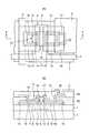
図1(A)はこの発明の第1実施形態としての薄膜トランジスタを備えた液晶表示素子の要部の透過平面図を示し、図1(B)は図1(A)のB−B線に沿う断面図を示す。この液晶表示素子はガラス基板1を備えている。ガラス基板1の上面には、マトリクス状に配置された複数の画素電極2と、各画素電極2に接続された薄膜トランジスタ3と、行方向に配置され、各薄膜トランジスタ3に走査信号を供給する走査ライン4と、列方向に配置され、各薄膜トランジスタ3にデータ信号を供給するデータライン5とが設けられている。(First embodiment)
FIG. 1A shows a transmission plan view of a main part of a liquid crystal display element having a thin film transistor as a first embodiment of the present invention, and FIG. 1B is taken along line BB in FIG. A cross-sectional view is shown. The liquid crystal display element includes a
すなわち、ガラス基板1の上面の所定の箇所にはクロムやアルミニウム系金属等からなるゲート電極6を含む走査ライン4が設けられている。ゲート電極6および走査ライン4を含むガラス基板1の上面には窒化シリコンからなるゲート絶縁膜7が設けられている。ゲート電極6上におけるゲート絶縁膜7の上面の所定の箇所には真性酸化亜鉛からなる半導体薄膜8が設けられている。 That is, a
ゲート電極6上における半導体薄膜8の上面中央部には窒化シリコンからなる中央保護膜9が設けられている。中央保護膜9の上面両側、その両側における半導体薄膜8の上面およびその近傍のゲート絶縁膜7の上面には、半導体薄膜8のチャネル流域上で相互に分離された、n型酸化亜鉛からなるオーミックコンタクト層10、11が設けられている。 A central
この場合、一方のオーミックコンタクト層10は、半導体薄膜8の図1(A)における右半分の右端面およびそれに直交する方向の両端面の3つの端面を覆うように設けられている。他方のオーミックコンタクト層11は、半導体薄膜8の図1(A)における左半分の左端面およびそれに直交する方向の両端面の3つの端面を覆うように設けられている。したがって、中央保護膜9下に設けられた半導体薄膜8の中央部の図1(A)における上下部の端面は、オーミックコンタクト層10、11によって覆われずに露出されている。 In this case, one
一方のオーミックコンタクト層10の周辺部上面および他方のオーミックコンタクト層11の周辺部上面には窒化シリコンからなる上面保護膜12、13が設けられている。すなわち、オーミックコンタクト層10、11の各周辺部を除く領域における上面保護膜12、13にはコンタクトホール14、15が設けられている。 Upper surface
上面保護膜12、13を含むゲート絶縁膜7の上面には窒化シリコンからなる上層絶縁膜16が設けられている。ここで、図1(B)を明確にする目的で、上層絶縁膜16には多数の点からなるハッチングが記入されている。そして、上層絶縁膜16には、上面保護膜12、13のコンタクトホール14、15に連続するコンタクトホール14、15が設けられている。 An upper
一方のコンタクトホール14を介して露出された一方のオーミックコンタクト層10の上面およびその近傍の上層絶縁膜16の上面にはクロム、アルミニウム系金属、ITO等からなるソース電極17が設けられている。他方のコンタクトホール15を介して露出された他方のオーミックコンタクト層11の上面、その近傍の上層絶縁膜16の上面および上層絶縁膜16の上面の所定の箇所にはクロム、アルミニウム系金属、ITO等からなるドレイン電極18を含むデータライン5が設けられている。 A
ここで、ゲート電極6、ゲート絶縁膜7、半導体薄膜8、中央保護膜9、オーミックコンタクト層10、11、上面保護膜12、13、ソース電極17およびドレイン電極18により、薄膜トランジスタ3が構成されている。 Here, the
そして、中央保護膜9の図1(A)における左右方向の寸法がチャネル長Lとなっている。また、例えば、他方のオーミックコンタクト層15を含むドレイン電極18と半導体薄膜8との接続部分つまり他方のコンタクトホール15の図1(A)における上下方向の寸法がチャネル幅Wとなっている。 The dimension of the central
ソース電極17、ドレイン電極18およびデータライン5を含む上層絶縁膜16の上面には窒化シリコンからなるオーバーコート膜19が設けられている。オーバーコート膜19の上面の所定の箇所にはITO等の透明導電材料からなる画素電極2が設けられている。画素電極2は、オーバーコート膜19の所定の箇所に設けられたコンタクトホール20を介してソース電極17に接続されている。 An
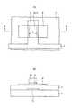
次に、この液晶表示素子における薄膜トランジスタ3の部分の製造方法の一例について説明する。まず、図2(A)、(B)に示すように、ガラス基板1の上面の所定の箇所に、スパッタ法により成膜されたクロムやアルミニウム系金属等からなる金属層をフォトリソグラフィ法によりパターニングすることにより、ゲート電極6を含む走査ライン4を形成する。 Next, an example of a method for manufacturing the portion of the
次に、ゲート電極6および走査ライン4を含むガラス基板1の上面に、プラズマCVD法により、窒化シリコンからなるゲート絶縁膜7、真性酸化亜鉛からなる半導体薄膜形成用層8aおよび窒化シリコンからなる中央保護膜形成用層9aを連続して成膜する。次に、中央保護膜形成用層9aの上面に、フォトリソグラフィ法により、デバイスエリア形成用のレジストパターン21を形成する。 Next, the
次に、レジストパターン21をマスクとして、中央保護膜形成用層9aをエッチングすると、図3(A)、(B)に示すように、レジストパターン21下に中央保護膜形成用層9bが残存される。この場合、レジストパターン21下以外の領域における半導体薄膜形成用層8aの表面が露出される。そこで、窒化シリコンからなる中央保護膜形成用層9aのエッチング方法としては、中央保護膜形成用層9aのエッチング速度は速いが、真性酸化亜鉛からなる半導体薄膜形成用層8aをなるべく侵さないようにするために、六フッ化イオウ(SF6)を用いた反応性プラズマエッチング(ドライエッチング)が好ましい。Next, when the central protective
次に、レジストパターン21をレジスト剥離液を用いて剥離する。この場合、中央保護膜形成用層9b下以外の領域における半導体薄膜形成用層8aの表面がレジスト剥離液に曝されるが、この曝された部分はデバイスエリア以外であるので、別に支障はない。 Next, the resist
次に、中央保護膜形成用層9bをマスクとして、半導体薄膜形成用層8aをエッチングすると、図4(A)、(B)に示すように、中央保護膜形成用層9b下に半導体薄膜8が形成される。この場合、真性酸化亜鉛からなる半導体薄膜形成用層8aのエッチング液としては、アルカリ水溶液を用いる。例えば、水酸化ナトリウム(NaOH)30wt%未満水溶液、好ましくは2〜10wt%水溶液を用いる。エッチング液の温度は、5〜40℃、好ましくは室温(22〜23℃)とする。 Next, when the semiconductor thin
そして、エッチング液として水酸化ナトリウム(NaOH)5wt%水溶液(温度は室温(22〜23℃))を用いたところ、エッチング速度は約80nm/分であった。ところで、エッチング速度は、加工の制御性を考慮した場合、余り大きいと膜厚や密度等のばらつきの要因のためエッチング終了の制御が難しく、勿論、小さすぎれば生産性が低下する。そこで、エッチング速度は、一般的に、100〜200nm/分程度が好ましいと言われている。エッチング速度が約80nm/分の水酸化ナトリウム(NaOH)5wt%水溶液は、一応、満足できる範囲と言える。 When an aqueous solution of sodium hydroxide (NaOH) 5 wt% (temperature is room temperature (22 to 23 ° C.)) was used as an etching solution, the etching rate was about 80 nm / min. By the way, when considering the controllability of processing, if the etching rate is too large, it is difficult to control the end of etching because of variations in film thickness, density, etc. Of course, if the etching rate is too small, the productivity is lowered. Therefore, it is generally said that the etching rate is preferably about 100 to 200 nm / min. A 5 wt% aqueous solution of sodium hydroxide (NaOH) with an etching rate of about 80 nm / min can be said to be a satisfactory range.
しかし、更に、生産効率を上げるために、ナトリウムの濃度を大きくしてもよい。また、エッチング液としてリン酸水溶液等の速度が大きいものを使用する場合、0.05%程度と極めて低濃度にしなければならないが、このように低濃度のものを用いる場合、被エッチング物の溶解により使用時における変質速度が大きいので、やはり制御が困難となる。従って、水酸化ナトリウム水溶液の場合、30wt%未満水溶液、好ましくは2〜10wt%程度の水溶液を適用することができるので、このような面で極めて有効である。 However, the concentration of sodium may be increased to increase production efficiency. In addition, when using an etching solution having a high speed, such as an aqueous phosphoric acid solution, the concentration must be extremely low, such as about 0.05%. As a result, the change rate during use is large, so that control becomes difficult. Accordingly, in the case of an aqueous sodium hydroxide solution, an aqueous solution of less than 30 wt%, preferably an aqueous solution of about 2 to 10 wt% can be applied, and this is extremely effective in this respect.
次に、図5(A)、(B)に示すように、中央保護膜形成用層9bの上面中央部に、フォトリソグラフィ法により、中央保護膜形成用のレジストパターン22を形成する。次に、レジストパターン22をマスクとして、中央保護膜形成用層9bをエッチングすると、図6(A)、(B)に示すように、レジストパターン22下に中央保護膜9が形成される。 Next, as shown in FIGS. 5A and 5B, a resist
この場合、レジストパターン22下以外の領域における半導体薄膜8の表面が露出される。したがって、窒化シリコンからなる中央保護膜形成用層9bのエッチング方法としては、上記と同様に、六フッ化イオウ(SF6)を用いた反応性プラズマエッチング(ドライエッチング)が好ましい。そして、中央保護膜9の図6(A)における左右方向の寸法により、チャネル長Lが決定される。In this case, the surface of the semiconductor
次に、レジストパターン22をレジスト剥離液を用いて剥離する。ここで、レジスト剥離液として、酸性もアルカリ性も呈さない(電解質を含まない)もの、例えば、単一の有機溶媒(例えばジメチルスルホキシド(DMSO))を用いても、レジスト剥離を良好に行えることは、発明者において確認されている。しかも、このようなレジスト剥離液は、中央保護膜9下以外の領域における半導体薄膜8の表面を全く侵さないため、ここではこのようなレジスト剥離液を用いる。 Next, the resist
次に、図7(A)、(B)に示すように、半導体薄膜8および中央保護膜9を含むゲート絶縁膜7の上面に、プラズマCVD法により、n型酸化亜鉛からなるオーミックコンタクト層形成用層23および窒化シリコンからなる上面保護膜形成用層24を連続して成膜する。次に、上面保護膜形成用層24の上面に、フォトリソグラフィ法により、上面保護膜形成用のレジストパターン25を形成する。 Next, as shown in FIGS. 7A and 7B, an ohmic contact layer made of n-type zinc oxide is formed on the upper surface of the
次に、レジストパターン25をマスクとして、上面保護膜形成用層24をエッチングすると、図8(A)、(B)に示すように、レジストパターン25下に上面保護膜12、13が形成される。この場合、レジストパターン25下以外の領域におけるn型酸化亜鉛からなるオーミックコンタクト層形成用層23の表面が露出される。したがって、窒化シリコンからなる上面保護膜形成用層24のエッチング方法としては、上記と同様に、六フッ化イオウ(SF6)を用いた反応性プラズマエッチング(ドライエッチング)が好ましい。Next, when the upper surface protective
また、この状態では、一方の上面保護膜12は、半導体薄膜8の図8(A)における右半分の右端面およびそれに直交する方向の両端面の3つの端面を覆い、且つ、中央保護膜9の図8(A)における右端面を覆うように形成されている。また、他方の上面保護膜13は、半導体薄膜8の図8(A)における左半分の左端面およびそれに直交する方向の両端面の3つの端面を覆い、且つ、中央保護膜9の図8(A)における左端面を覆うように形成されている。 Further, in this state, one upper surface
次に、レジストパターン25をレジスト剥離液を用いて剥離する。この場合、上面保護膜12、13下以外の領域におけるn型酸化亜鉛からなるオーミックコンタクト層形成用層23の表面がレジスト剥離液に曝されるが、この曝された部分はオーミックコンタクト層形成領域以外であるので、別に支障はない。 Next, the resist
次に、上面保護膜12、13をマスクとして、オーミックコンタクト層形成用層23をエッチングすると、図9(A)、(B)に示すように、上面保護膜12、13下にオーミックコンタクト層10、11が形成される。この場合、オーミックコンタクト層形成用層23はn型酸化亜鉛によって形成されているため、エッチング液として上記水酸化ナトリウム水溶液を用いると、加工の制御性を良好とすることができる。 Next, when the ohmic contact
また、この場合、半導体薄膜8の中央部の図9(A)における上下部の端面以外の端面は上面保護膜12、13によって覆われ、保護されている。また、半導体薄膜8の上面中央部は中央保護膜9および上面保護膜12、13によって覆われ、保護されている。したがって、半導体薄膜8の中央部の図9(A)における上下部の端面にサイドエッチングがやや生じるが、後述の如く、チャネル幅Wに影響を与えることはない。 In this case, the end surfaces other than the upper and lower end surfaces in FIG. 9A at the center of the semiconductor
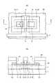
次に、図10(A)、(B)に示すように、上面保護膜12、13を含むゲート絶縁膜7の上面に、プラズマCVD法により、窒化シリコンからなる上層絶縁膜16を成膜する。次に、上層絶縁膜16の上面に、フォトリソグラフィ法により、コンタクトホール形成用のレジストパターン26を形成する。 Next, as shown in FIGS. 10A and 10B, an upper insulating
次に、レジストパターン26をマスクとして、上層絶縁膜16および上面保護膜12、13を連続してエッチングすると、図11(A)、(B)に示すように、上層絶縁膜16および上面保護膜12、13の所定の箇所に2つのコンタクトホール14、15が連続して形成される。この場合、上層絶縁膜16および上面保護膜12、13にコンタクトホール14、15を連続して形成するため、上層絶縁膜16の材料は、上面保護膜12、13の材料と同じであることが好ましく、この実施形態では窒化シリコンである。 Next, when the upper insulating
また、この場合、コンタクトホール14、15内におけるn型酸化亜鉛からなるオーミックコンタクト層10、11の上面が露出される。したがって、窒化シリコンからなる上層絶縁膜16および上面保護膜12、13にコンタクトホール14、15を形成するためのエッチング方法としては、上記と同様に、六フッ化イオウ(SF6)を用いた反応性プラズマエッチング(ドライエッチング)が好ましい。In this case, the upper surfaces of the ohmic contact layers 10 and 11 made of n-type zinc oxide in the contact holes 14 and 15 are exposed. Therefore, as an etching method for forming the contact holes 14 and 15 in the upper insulating
次に、レジストパターン26をレジスト剥離液を用いて剥離する。この場合、コンタクトホール14、15内におけるn型酸化亜鉛からなるオーミックコンタクト層10、11の上面が露出されている。したがって、この場合のレジスト剥離液としては、酸性もアルカリ性も呈さない(電解質を含まない)もの、例えば、単一の有機溶媒(例えばジメチルスルホキシド(DMSO))を用いる。 Next, the resist
ここで、例えば、他方のオーミックコンタクト層15を含むドレイン電極18と半導体薄膜8との接続部分つまり他方のコンタクトホール15の図11(A)における上下方向の寸法がチャネル幅Wとなる。このチャネル幅Wは、半導体薄膜8の図11(A)における上下方向の寸法よりもある程度小さい。したがって、図9(A)、(B)に示す工程において、半導体薄膜8の中央部の図9(A)における上下部の端面にサイドエッチングがやや生じたとしても、チャネル幅Wに影響を与えることはない。 Here, for example, the vertical dimension in FIG. 11A of the connection portion between the
次に、図12(A)、(B)に示すように、オーミックコンタクト層10、11を含む上層絶縁膜16の上面に、スパッタ法により、クロム、アルミニウム系金属、ITO等からなるソース・ドレイン電極等形成用層27を成膜する。次に、ソース・ドレイン電極等形成用層27の上面に、フォトリソグラフィ法により、ソース・ドレイン電極等形成用のレジストパターン28を形成する。 Next, as shown in FIGS. 12A and 12B, a source / drain made of chromium, an aluminum-based metal, ITO, or the like is formed on the upper surface of the upper insulating
次に、レジストパターン28をマスクとして、ソース・ドレイン電極等形成用層27をエッチングすると、図13(A)、(B)に示すように、レジストパターン28下にソース電極17、ドレイン電極18およびデータライン5が形成される。次に、レジストパターン28をレジスト剥離液を用いて剥離する。 Next, when the source / drain
この場合、コンタクトホール14、15内のオーミックコンタクト層10、11はソース電極17およびドレイン電極18によって完全に覆われている。したがって、ソース・ドレイン電極等形成用層27を成膜した後においては、オーミックコンタクト層10、11は、ソース・ドレイン電極等形成用層27をエッチングするためのエッチング液およびレジスト剥離液等に曝されることはなく、完全に保護されている。これにより、加工精度を良くすることができる。 In this case, the ohmic contact layers 10 and 11 in the contact holes 14 and 15 are completely covered with the
次に、図1(A)、(B)に示すように、ソース電極17、ドレイン電極18およびデータライン5を含む上層絶縁膜16の上面に、プラズマCVD法により、窒化シリコンからなるオーバーコート膜19を成膜する。次に、オーバーコート膜19の所定の箇所に、フォトリソグラフィ法により、コンタクトホール20を形成する。次に、オーバーコート膜19の上面の所定の箇所に、スパッタ法により成膜されたITO等の透明導電材料からなる画素電極形成用層をフォトリソグラフィ法によりパターニングすることにより、画素電極2をコンタクトホール20を介してソース電極17に接続させて形成する。 Next, as shown in FIGS. 1A and 1B, an overcoat film made of silicon nitride is formed on the upper surface of the upper insulating
以上のように、上記製造方法では、半導体薄膜8の中央部上面にその所定方向の寸法によりチャネル長Lを決定する中央保護膜9を形成し、オーミックコンタクト層10、11の周辺部上面に上面保護膜12、13を形成し、上面保護膜12、13にその所定方向の寸法によりチャネル幅Wを決定する2つのコンタクトホール14、15を形成しているので、半導体薄膜8にサイドエッチングがやや生じても、中央保護膜9および上面保護膜12、13に形成された2つのコンタクトホール14、15によって決定されるチャネル長Lおよびチャネル幅Wに寸法変化が生じることはなく、加工精度を良くすることができる。 As described above, in the above manufacturing method, the central
なお、半導体薄膜形成用層8aおよびオーミックコンタクト層形成用層23の成膜は、プラズマCVD法に限らず、スパッタ法、蒸着法、キャスト法、メッキ法等であってもよい。また、オーミックコンタクト層10、11は、n型酸化亜鉛に限らず、p型酸化亜鉛であってもよく、また酸素欠損を生じさせて導電率を変化させた酸化亜鉛層であってもよい。 The formation of the semiconductor thin
また、上記実施形態では、半導体薄膜8の中央部上面に中央保護膜9を設けているが、半導体薄膜8を十分な厚さにすれば、エッチングによりオーミックコンタクト層形成用層23を分離して、オーミックコンタクト層10、11を形成する際、多少、半導体薄膜8がエッチングされたとしても、残りの半導体薄膜8の厚さを十分なものにすることができるので、中央保護膜9を形成せず、半導体薄膜8上に直接、オーミックコンタクト層10、11を形成することができる。 In the above embodiment, the central
1 ガラス基板
2 画素電極
3 薄膜トランジスタ
4 走査ライン
5 データライン
6 ゲート電極
7 ゲート絶縁膜
8 半導体薄膜
9 中央保護膜
10、11 オーミックコンタクト層
12、13 上面保護膜
14、15 コンタクトホール
16 上層絶縁膜
17 ソース電極
18 ドレイン電極
19 オーバーコート膜
20 コンタクトホールDESCRIPTION OF
Claims (8)
Translated fromJapanese前記半導体薄膜の上層側に第1のパターン形状にパターニングされた絶縁膜からなる上面保護膜と、
前記第1のパターン形状にパターニングされる前の第2のパターン形状を有した前記絶縁膜をマスクにして、該絶縁膜の下層側に、前記半導体薄膜の前記ゲート電極に重畳する領域とは異なる領域の前記半導体薄膜における端面の全てを覆うように、前記第2のパターン形状にパターニングされたn型酸化亜鉛からなるオーミックコンタクト層と、
前記第1のパターン形状にパターニングされた前記絶縁膜に形成されているそれぞれに対応するコンタクトホールを介して、前記オーミックコンタクト層に接続されたソース電極およびドレイン電極と、
前記半導体薄膜と前記オーミックコンタクト層との間の層として形成されるとともに、前記ゲート電極に重畳する領域であって前記オーミックコンタクト層から露出する領域における前記半導体薄膜の少なくとも一部を覆うように形成された中央保護膜と、
を具備することを特徴とする薄膜トランジスタ。A semiconductor thin film made of zinc oxide formed on the gate electrode via the gate insulating film;
An upper surface protective film made of an insulating film patterned in a first pattern shape on the upper side of the semiconductor thin film;
The insulating film having the second pattern shape before being patterned into the first pattern shape is used as a mask, and is different from the region overlapping the gate electrode of the semiconductor thin film on the lower layer side of the insulating film An ohmic contact layer made of n-type zinc oxide patterned in the second pattern shape so as to cover the entire end face of the semiconductor thin film in the region;
A source electrode and a drain electrode connected to the ohmic contact layer via respective contact holes formed in the insulating film patterned in the first pattern shape;
It is formed as a layer between the semiconductor thin film and the ohmic contact layer, and is formed so as to cover at least a part of the semiconductor thin film in a region overlapping with the gate electrode and exposed from the ohmic contact layer A central protective film,
A thin film transistor comprising:
前記ソース電極および前記ドレイン電極がそれぞれに対応した前記開口部を介して前記オーミックコンタクト層に接続されていることを特徴とする請求項1から3の何れかに記載の薄膜トランジスタ。An upper insulating film formed on the ohmic contact layer patterned in the second pattern shape through the upper surface protective film, and having an opening formed at a position corresponding to the contact hole;
4. The thin film transistor according to claim 1, wherein the source electrode and the drain electrode are connected to the ohmic contact layer through the corresponding openings. 5.
前記ゲート電極に重畳する領域における前記半導体薄膜上に中央保護膜を形成した後、前記半導体薄膜の上層側にn型酸化亜鉛からなるオーミックコンタクト層を成膜し、
前記オーミックコンタクト層上に所定のパターン形状を有する絶縁膜からなる上面保護膜を形成し、
前記所定のパターン形状を有する前記絶縁膜をマスクにして、前記半導体薄膜の前記ゲート電極に重畳する領域とは異なる領域の前記半導体薄膜における端面の全てが覆われるように、前記オーミックコンタクト層を前記所定のパターン形状にパターニングし、
前記所定のパターン形状にパターニングされた前記オーミックコンタクト層の一部が露出するように前記所定のパターン形状を有する絶縁膜にコンタクトホールを形成し、
それぞれに対応する前記コンタクトホールを介して前記オーミックコンタクト層に接続するようにソース電極およびドレイン電極を形成することを特徴とする薄膜トランジスタの製造方法。A method of manufacturing a thin film transistor having a semiconductor thin film made of zinc oxide formed on a gate electrode through a gate insulating film,
After forming a central protective film on the semiconductor thin film in a region overlapping with the gate electrode, an ohmic contact layer made of n-type zinc oxideis formed on the upper side of the semiconductor thin film,
Forming an upper surface protective film made of an insulating film having a predetermined pattern shape on the ohmic contact layer;
Using the insulating film having the predetermined pattern shape as a mask, the ohmic contact layer is formed so that the entire end surface of the semiconductor thin film in a region different from the region overlapping the gate electrode of the semiconductor thin film is covered. Pattern it into a predetermined pattern shape,
Forming a contact hole in the insulating film having the predetermined pattern shape so that a part of the ohmic contact layer patterned in the predetermined pattern shape is exposed;
A method of manufacturing a thin film transistor, comprising forming a source electrode and a drain electrode so as to be connected to the ohmic contact layer through the corresponding contact holes.
その後、前記上層絶縁膜及び前記所定のパターン形状を有する絶縁膜に、前記所定のパターン形状にパターニングされた前記オーミックコンタクト層の一部が露出するように、開口部としてのコンタクトホールを形成し、
その後、前記ソース電極およびドレイン電極を形成することを特徴とする請求項5から7の何れかに記載の薄膜トランジスタの製造方法。Forming an upper insulating film on the ohmic contact layer patterned in the predetermined pattern shape through the insulating film having the predetermined pattern shape,
Thereafter, a contact hole as an opening is formed in the upper insulating film and the insulating film having the predetermined pattern shape so that a part of the ohmic contact layer patterned in the predetermined pattern shape is exposed,
8. The method of manufacturing a thin film transistor according to claim 5, wherein the source electrode and the drain electrode are formed thereafter.
Priority Applications (1)
| Application Number | Priority Date | Filing Date | Title |
|---|---|---|---|
| JP2004378475AJP4569295B2 (en) | 2004-12-28 | 2004-12-28 | Thin film transistor and manufacturing method thereof |
Applications Claiming Priority (1)
| Application Number | Priority Date | Filing Date | Title |
|---|---|---|---|
| JP2004378475AJP4569295B2 (en) | 2004-12-28 | 2004-12-28 | Thin film transistor and manufacturing method thereof |
Publications (2)
| Publication Number | Publication Date |
|---|---|
| JP2006186119A JP2006186119A (en) | 2006-07-13 |
| JP4569295B2true JP4569295B2 (en) | 2010-10-27 |
Family
ID=36739013
Family Applications (1)
| Application Number | Title | Priority Date | Filing Date |
|---|---|---|---|
| JP2004378475AExpired - Fee RelatedJP4569295B2 (en) | 2004-12-28 | 2004-12-28 | Thin film transistor and manufacturing method thereof |
Country Status (1)
| Country | Link |
|---|---|
| JP (1) | JP4569295B2 (en) |
Families Citing this family (16)
| Publication number | Priority date | Publication date | Assignee | Title |
|---|---|---|---|---|
| KR100793105B1 (en) | 2006-12-07 | 2008-01-10 | 엘지전자 주식회사 | Flat panel display device including thin film transistor and thin film transistor and manufacturing method thereof |
| KR101410926B1 (en)* | 2007-02-16 | 2014-06-24 | 삼성전자주식회사 | Thin film transistor and manufacturing method thereof |
| KR20090011704A (en) | 2007-07-27 | 2009-02-02 | 삼성전자주식회사 | Thin film transistor substrate and its manufacturing method |
| US7768008B2 (en) | 2007-11-13 | 2010-08-03 | Toppan Printing Co., Ltd. | Thin film transistor, method for manufacturing the same and display using the same |
| JP5704790B2 (en)* | 2008-05-07 | 2015-04-22 | キヤノン株式会社 | Thin film transistor and display device |
| TWI627757B (en) | 2008-07-31 | 2018-06-21 | 半導體能源研究所股份有限公司 | Semiconductor device |
| TWI424506B (en) | 2008-08-08 | 2014-01-21 | Semiconductor Energy Lab | Semiconductor device manufacturing method |
| TWI633371B (en)* | 2008-12-03 | 2018-08-21 | 半導體能源研究所股份有限公司 | Liquid crystal display device |
| US8174021B2 (en)* | 2009-02-06 | 2012-05-08 | Semiconductor Energy Laboratory Co., Ltd. | Semiconductor device and method of manufacturing the semiconductor device |
| WO2011027664A1 (en)* | 2009-09-04 | 2011-03-10 | Semiconductor Energy Laboratory Co., Ltd. | Liquid crystal display device and method for manufacturing the same |
| WO2011070901A1 (en)* | 2009-12-11 | 2011-06-16 | Semiconductor Energy Laboratory Co., Ltd. | Semiconductor device and manufacturing method thereof |
| US8624239B2 (en)* | 2010-05-20 | 2014-01-07 | Semiconductor Energy Laboratory Co., Ltd. | Semiconductor device |
| JP2012204548A (en)* | 2011-03-24 | 2012-10-22 | Sony Corp | Display device and manufacturing method therefor |
| KR20130092848A (en)* | 2012-02-13 | 2013-08-21 | 삼성전자주식회사 | Thin film transistor and display panel employing the same |
| KR101438642B1 (en)* | 2013-11-04 | 2014-09-17 | 삼성전자주식회사 | Thin film transistor and method for forming the same |
| KR101987800B1 (en)* | 2019-02-08 | 2019-10-01 | 삼성디스플레이 주식회사 | Thin film transistor array panel and manufacturing method for a thin film transistor array panel |
Family Cites Families (2)
| Publication number | Priority date | Publication date | Assignee | Title |
|---|---|---|---|---|
| JPS61145582A (en)* | 1984-12-20 | 1986-07-03 | キヤノン株式会社 | display device |
| JP3403897B2 (en)* | 1996-08-02 | 2003-05-06 | シャープ株式会社 | Active matrix substrate |
- 2004
- 2004-12-28JPJP2004378475Apatent/JP4569295B2/ennot_activeExpired - Fee Related
Also Published As
| Publication number | Publication date |
|---|---|
| JP2006186119A (en) | 2006-07-13 |
Similar Documents
| Publication | Publication Date | Title |
|---|---|---|
| JP5333160B2 (en) | Thin film transistor and manufacturing method thereof | |
| JP2006100760A (en) | Thin film transistor and manufacturing method thereof | |
| JP4569295B2 (en) | Thin film transistor and manufacturing method thereof | |
| JP2006344849A (en) | Thin film transistor | |
| JP5413549B2 (en) | Thin film transistor panel and manufacturing method thereof | |
| JP4958764B2 (en) | Method for manufacturing array substrate for liquid crystal display device | |
| JP5324111B2 (en) | Thin film transistor array panel and manufacturing method thereof | |
| JP5332091B2 (en) | Thin film transistor manufacturing method | |
| JP2015501549A (en) | Thin film transistor array substrate | |
| JP4458048B2 (en) | Thin film transistor manufacturing method | |
| JP2006269469A (en) | Thin film transistor and manufacturing method thereof | |
| CN114335018A (en) | Preparation method of display panel and display panel | |
| JP5200366B2 (en) | Thin film transistor panel and manufacturing method thereof | |
| JP5228295B2 (en) | Manufacturing method of semiconductor device | |
| KR20080057386A (en) | Display substrate and manufacturing method thereof | |
| KR20090129824A (en) | Thin film transistor substrate and its manufacturing method | |
| KR100701069B1 (en) | How to form a short prevention pattern between data lines | |
| KR20070053490A (en) | Manufacturing Method of Display Board | |
| KR20070091732A (en) | Manufacturing method of display board | |
| KR20090071109A (en) | Thin film transistor array substrate and its manufacturing method | |
| KR20080040319A (en) | Display substrate and manufacturing method thereof |
Legal Events
| Date | Code | Title | Description |
|---|---|---|---|
| RD04 | Notification of resignation of power of attorney | Free format text:JAPANESE INTERMEDIATE CODE: A7424 Effective date:20080519 | |
| A977 | Report on retrieval | Free format text:JAPANESE INTERMEDIATE CODE: A971007 Effective date:20080829 | |
| A131 | Notification of reasons for refusal | Free format text:JAPANESE INTERMEDIATE CODE: A131 Effective date:20080916 | |
| A521 | Request for written amendment filed | Free format text:JAPANESE INTERMEDIATE CODE: A523 Effective date:20081027 | |
| A131 | Notification of reasons for refusal | Free format text:JAPANESE INTERMEDIATE CODE: A131 Effective date:20090623 | |
| A521 | Request for written amendment filed | Free format text:JAPANESE INTERMEDIATE CODE: A523 Effective date:20090703 | |
| A02 | Decision of refusal | Free format text:JAPANESE INTERMEDIATE CODE: A02 Effective date:20100126 | |
| A521 | Request for written amendment filed | Free format text:JAPANESE INTERMEDIATE CODE: A523 Effective date:20100301 | |
| A911 | Transfer to examiner for re-examination before appeal (zenchi) | Free format text:JAPANESE INTERMEDIATE CODE: A911 Effective date:20100510 | |
| TRDD | Decision of grant or rejection written | ||
| A01 | Written decision to grant a patent or to grant a registration (utility model) | Free format text:JAPANESE INTERMEDIATE CODE: A01 Effective date:20100713 | |
| A01 | Written decision to grant a patent or to grant a registration (utility model) | Free format text:JAPANESE INTERMEDIATE CODE: A01 | |
| A61 | First payment of annual fees (during grant procedure) | Free format text:JAPANESE INTERMEDIATE CODE: A61 Effective date:20100726 | |
| FPAY | Renewal fee payment (event date is renewal date of database) | Free format text:PAYMENT UNTIL: 20130820 Year of fee payment:3 | |
| R150 | Certificate of patent or registration of utility model | Free format text:JAPANESE INTERMEDIATE CODE: R150 | |
| LAPS | Cancellation because of no payment of annual fees |