JP4566599B2 - Semiconductor device and manufacturing method thereof - Google Patents
Semiconductor device and manufacturing method thereofDownload PDFInfo
- Publication number
- JP4566599B2 JP4566599B2JP2004095919AJP2004095919AJP4566599B2JP 4566599 B2JP4566599 B2JP 4566599B2JP 2004095919 AJP2004095919 AJP 2004095919AJP 2004095919 AJP2004095919 AJP 2004095919AJP 4566599 B2JP4566599 B2JP 4566599B2
- Authority
- JP
- Japan
- Prior art keywords
- layer
- gate electrode
- contact hole
- silicide layer
- insulating film
- Prior art date
- Legal status (The legal status is an assumption and is not a legal conclusion. Google has not performed a legal analysis and makes no representation as to the accuracy of the status listed.)
- Expired - Fee Related
Links
Images


Classifications
- H—ELECTRICITY
- H10—SEMICONDUCTOR DEVICES; ELECTRIC SOLID-STATE DEVICES NOT OTHERWISE PROVIDED FOR
- H10B—ELECTRONIC MEMORY DEVICES
- H10B10/00—Static random access memory [SRAM] devices
- H—ELECTRICITY
- H10—SEMICONDUCTOR DEVICES; ELECTRIC SOLID-STATE DEVICES NOT OTHERWISE PROVIDED FOR
- H10B—ELECTRONIC MEMORY DEVICES
- H10B10/00—Static random access memory [SRAM] devices
- H10B10/12—Static random access memory [SRAM] devices comprising a MOSFET load element
Landscapes
- Semiconductor Memories (AREA)
- Electrodes Of Semiconductors (AREA)
- Internal Circuitry In Semiconductor Integrated Circuit Devices (AREA)
Description
Translated fromJapanese本発明は半導体装置に関し、特に、付加抵抗を備えたSRAM(スタティック型ランダムアクセスメモリ)等の半導体記憶装置に適用して好適な半導体装置とその製造方法に関する。 The present invention relates to a semiconductor device, and more particularly to a semiconductor device suitable for application to a semiconductor memory device such as an SRAM (Static Random Access Memory) having an additional resistor and a method for manufacturing the same.
近年、SRAMにおけるチップサイズ、ないしメモリセルの縮小化並びに大容量化が進むにつれてSER(Soft Error Rate )耐性の低下が問題になっている。このSERは、α線、宇宙線が例えば半導体基板に入射されると多数の電子・正孔対が発生し、SRAMのメモリセルを構成している対をなすNMOSトランジスタ(NチャネルMOSトランジスタ)の一方のNMOSトランジスタのドレインに収集される。これにより、当該NMOSトランジスタのゲートに接続される一方の記憶ノード(Hノード)の電位がハイレベル(H)からローレベル(L)に変化し、この変化は対をなす他方のNMOSトランジスタのゲートに接続される記憶ノード(対極ノード)の電位がローレベル(L)からハイレベル(H)に変化し、結果として当該メモリセルの記憶情報が破壊されることになる。 In recent years, a reduction in SER (Soft Error Rate) resistance has become a problem as the chip size in an SRAM or the reduction in memory cells and the increase in capacity thereof have progressed. The SER is an NMOS transistor (N-channel MOS transistor) that forms a SRAM memory cell when α-rays and cosmic rays are incident on a semiconductor substrate, for example, to generate a large number of electron-hole pairs. Collected at the drain of one NMOS transistor. As a result, the potential of one storage node (H node) connected to the gate of the NMOS transistor changes from a high level (H) to a low level (L), and this change is caused by the gate of the other NMOS transistor forming a pair. The potential of the storage node (counter electrode node) connected to is changed from the low level (L) to the high level (H), and as a result, the storage information of the memory cell is destroyed.
このようなSER耐性の向上を図るための技術として、メモリセルのノードに抵抗や容量を付加し、これら付加抵抗と付加容量との積で決まる時定数CRで、α線、宇宙線などにより生じるHノード電位の低下時に対極ノードがハイレベル(H)になるのを遅らせてSER耐性を向上させる技術が提案されている。特に、付加抵抗を設ける技術として特許文献1〜4の技術がある。 As a technique for improving such SER resistance, a resistance or a capacitance is added to a node of a memory cell, and a time constant CR determined by a product of the additional resistance and the additional capacitance is generated by α rays, cosmic rays, or the like. There has been proposed a technique for improving the SER resistance by delaying the counter electrode node from becoming a high level (H) when the H node potential is lowered. In particular, there are techniques of
特許文献1の技術は、付加抵抗を接続しないMOSトランジスタのゲート電極を半導体層と金属半導体化合物層とを積層した構造、いわゆるサリサイド構造とし、付加抵抗を接続するゲート電極を半導体層のみの構造とすることで、当該半導体層の抵抗を付加抵抗として利用する技術である。この技術は特許文献2においてもほぼ同様であり、特許文献2では特にSRAMのSERについては触れられていないが、配線中に高抵抗を付加する技術として、配線をサリサイド構造とノンサリサイド構造とを併存させ、ノンサリサイド構造ではない領域においてバリアメタルを介在しない構造のコンタクトを形成することで当該コンタクトにつながる配線の高抵抗化を図る技術である。また、特許文献3の技術は、ゲート電極を構成する半導体層の一部に不純物濃度の低い領域を設け、この低不純物濃度の領域を高抵抗化して付加抵抗として構成したものである。さらに、特許文献4の技術は、MOSトランジスタのゲートとノードとの接続部を金属層とポリシリコン層との積層構造とし、この金属層とポリシリコン層との接触抵抗を付加抵抗として利用する技術である。
特許文献1〜4の技術はいずれも低抵抗の領域の一部に高抵抗の領域を形成する技術に基づくものである。すなわち、特許文献1,2はサリサイド構造をした低抵抗の領域の一部にノンサリサイド構造の領域を形成して高抵抗を形成しており、特許文献3は低抵抗の領域の一部の不純物濃度を低くして高抵抗を形成しており、特許文献4は低抵抗の領域の一部にポリシリコン層を形成して高抵抗を形成している。このため、特許文献1〜4のいずれも高抵抗の領域を形成するためにリソグラフィ技術が必要であり、特に微細化が進んだSRAMのメモリセル内の一部に高抵抗の領域を形成するためには極めて微小でかつ高い寸法精度のリソグラフィパターンが必要となり、高抵抗を高精度に製造することが困難なものになる。また、SRAMのメモリセル中において高抵抗としたくない箇所への影響を避ける為には、高抵抗を製造するためのリソグラフィパターンにある程度のマージンを取る必要があり、そのマージンの分だけメモリセルサイズが増大するという問題も生じる。 The techniques of
本発明の目的は、高精度なリソグラフィ技術を不要にして付加抵抗を含む配線を容易に製造することを可能にするとともに、リソグラフィ工程におけるマージンを緩和してメモリセルサイズの縮小化を図った半導体装置及びその製造方法を提供するものである。 An object of the present invention is to make it possible to easily manufacture a wiring including an additional resistor without using a high-precision lithography technique, and to reduce a memory cell size by reducing a margin in a lithography process. An apparatus and a method for manufacturing the same are provided.
本発明は、一対のMOSトランジスタからなる駆動トランジスタを備え、一方の駆動トランジスタのゲート電極と他方の駆動トランジスタのドレインとをノード配線により接続するとともに、当該ノード配線に付加抵抗を接続したメモリセルを備えるSRAM構成の半導体装置に適用する場合に、ゲート電極を半導体層上にシリサイド層を有するサリサイド構造とし、ゲート電極の上層に配設されるノード配線をゲート電極にコンタクトで接続し、当該コンタクトの底面においてのみシリサイド層が存在しない構成とする。この場合、導体層又はゲート電極を覆う層間絶縁膜を備え、層間絶縁膜に開口されたコンタクトホールを通して上層配線又はノード配線が導体層又はゲート電極に接続する構成とされ、コンタクトホールの底面においてのみシリサイド層が存在していない構成とする。The present invention includes a memory transistor including a driving transistor including a pair ofMOS transistors , the gate electrode of one driving transistor and the drain of the other driving transistor are connected by a node wiring, and an additional resistor is connected to the node wiring. When applied to a semiconductor device having an SRAM structure, the gate electrodehas a salicide structurehaving a silicide layer on the semiconductor layer, and a node wiring disposed on the gate electrode is connected to the gate electrode by a contact.The silicide layer does not exist only on thebottom surface . In this case, an interlayer insulating film covering the conductor layer or the gate electrode is provided, and the upper layer wiring or the node wiring is connected to the conductor layer or the gate electrode through the contact hole opened in the interlayer insulating film, and only on the bottom surface of the contact hole. The silicide layer is not present.
本発明は一対のMOSトランジスタからなる駆動トランジスタを備え、一方の駆動トランジスタのゲート電極と他方の駆動トランジスタのドレインとをノード配線により接続するとともに、当該ノード配線に付加抵抗を接続したメモリセルを備えるSRAM構成の半導体装置を製造する際には、半導体層上にシリサイド層を有するサリサイド構造のゲート電極と、ソース・ドレイン領域とを備える複数のMOSトランジスタを形成する工程と、前記MOSトランジスタを覆う層間絶縁膜を形成する工程と、少なくとも前記MOSトランジスタのうち前記駆動トランジスタのゲート電極に電気接続を行うためのコンタクトホールを前記層間絶縁膜に開口する工程と、前記駆動トランジスタのゲート電極に電気接続を行うコンタクトホールの底面に露呈された前記シリサイド層を除去する工程と、前記コンタクトホールを通して前記ゲート電極に電気接続されるノード配線を形成する工程を含んでいる。The present invention includesa driving transistor including a pair ofMOS transistors , and includes a memory cell in which a gate electrode of one driving transistor and a drain of the other driving transistor are connected by a node wiring, and an additional resistor is connected to the node wiring. When manufacturing a semiconductor device having an SRAM structure, a step of forming a plurality of MOS transistors each having a salicide structure gate electrode having a silicide layer on the semiconductor layer and source / drain regions, and an interlayer covering the MOS transistor Forming an insulating film; opening a contact hole in the interlayer insulating film for electrical connection to a gate electrode of the driving transistor of at least the MOS transistor; and electrically connecting the gate electrode of the driving transistor. Bottom of contact hole to be made Removing the being exposed said silicide layer includes a step of forming a node wiring to be electrically connected to the gate electrode through the contact hole.
本発明の製造方法においては、駆動トランジスタのゲート電極に電気接続を行うコンタクトホールと共に当該コンタクトホール以外の他のコンタクトホールを同時に開口した後、当該他のコンタクトホールをマスクで覆う工程を備え、マスクで覆われていないコンタクトホール内のシリサイド層を除去することが好ましい。また、層間絶縁膜の表面に前記シリサイド層とのエッチング選択比の大きなエッチングストッパ層を形成する工程を備えることが好ましい。 The manufacturing method of the present invention includes a step of simultaneously opening a contact hole other than the contact hole together with the contact hole for electrical connection to the gate electrode of the driving transistor, and then covering the other contact hole with a mask. It is preferable to remove the silicide layer in the contact hole not covered with. Further, it is preferable to provide a step of forming an etching stopper layer having a large etching selectivity with the silicide layer on the surface of the interlayer insulating film.
本発明の半導体装置によれば、ノード配線が電気接続されるゲート電極には、当該接続のコンタクト領域にシリサイド層が存在せず、ゲート電極に直接接続されているため、シリサイド層による低抵抗化が行われず、これらのコンタクトにおける電気抵抗が高くなり、結果としてノード配線に高抵抗を付加した配線となる。According to the semiconductor device of the presentinvention, sincethe node wiring theRuge over gate electrode is electrically connected, absent silicide layer in the contact region of the connectionis connected directly to theGate electrode, resistance reduction is not performed by the silicide layer, the electric resistance becomes high in these contacts, the result was obtained by adding the high resistancenode wiring lines.
また、本発明の製造方法では、層間絶縁膜に開口したコンタクトホールを利用した自己整合法によって導体層又はゲート電極上のシリサイド層を除去しているので、サリサイドを選択的に形成するための高精度のリソグラフィ工程が不要になり、製造が容易なものになる。また、シリサイド層を選択的に除去する際にコンタクトホールを利用した自己整合法を利用しているので、リソグラフィパターンにある程度のマージンを確保する必要はなく、メモリセルサイズが増大することもない。 In the manufacturing method of the present invention, the silicide layer on the conductor layer or the gate electrode is removed by the self-alignment method using the contact hole opened in the interlayer insulating film. An accurate lithography process is not required, and manufacturing is easy. Further, since the self-alignment method using contact holes is used when the silicide layer is selectively removed, it is not necessary to secure a certain margin in the lithography pattern, and the memory cell size does not increase.
本発明の実施例1を図面を参照して説明する。図1は本発明を6個のMOSトランジスタで構成した、いわゆる6Trメモリセルで構成されるSRAMに適用した実施例1の等価回路図である。図1に示すように、前記メモリセルMCはそれぞれNMOSトランジスタ(NチャネルMOSトランジスタ)からなる一対の駆動トランジスタQ3,Q4と、これら駆動トランジスタQ3,Q4にそれぞれソース・ドレインが縦続接続されるPMOSトランジスタ(PチャネルMOSトランジスタ)からなる一対の負荷トランジスタQ1,Q2と、これら駆動トランジスタQ3,Q4と負荷トランジスタQ1,Q2の接続点であるノードN1,N2にソース・ドレインが接続されるNMOSトランジスタからなる一対の転送トランジスタQ5,Q6とで構成されている。 A first embodiment of the present invention will be described with reference to the drawings. FIG. 1 is an equivalent circuit diagram of a first embodiment in which the present invention is applied to an SRAM composed of so-called 6Tr memory cells composed of six MOS transistors. As shown in FIG. 1, the memory cell MC includes a pair of drive transistors Q3 and Q4 each composed of an NMOS transistor (N-channel MOS transistor), and a PMOS transistor whose source and drain are connected in cascade to the drive transistors Q3 and Q4, respectively. A pair of load transistors Q1 and Q2 composed of (P-channel MOS transistors), and an NMOS transistor whose source and drain are connected to nodes N1 and N2 which are connection points of the drive transistors Q3 and Q4 and the load transistors Q1 and Q2. It is composed of a pair of transfer transistors Q5 and Q6.
すなわち、一方の前記負荷トランジスタQ1のソースは電源VDDに接続され、ドレインは駆動トランジスタQ3のドレインに接続され、ゲートは駆動トランジスタQ3のゲートに接続される。また、駆動トランジスタQ3のソースは接地GNDに接続される。前記駆動トランジスタQ3のドレインは第1ノードとして付加抵抗R1を含むノード配線NL1によって対向する駆動トランジスタQ4のゲートに接続される。さらに、前記駆動トランジスタQ3のドレインは転送トランジスタQ5を介してデジット線DL1に接続されている。また、他方の前記負荷トランジスタQ2のソースは電源VDDに接続され、ドレインは駆動トランジスタQ4のドレインに接続され、ゲートは駆動トランジスタQ4のゲートに接続される。また、駆動トランジスタQ4のソースは接地GNDに接続される。前記駆動トランジスタQ4のドレインは第2ノードN2として付加抵抗R2を含むノード配線NL2によって対向する駆動トランジスタQ3のゲートに接続される。前記駆動トランジスタQ4のドレインは転送トランジスタQ6を介してデジット線DL2に接続されている。そして、これら転送トランジスタQ5,Q6の各ゲートはワード線WLに接続されている。 That is, the source of one of the load transistors Q1 is connected to the power supply VDD, the drain is connected to the drain of the driving transistor Q3, and the gate is connected to the gate of the driving transistor Q3. The source of the driving transistor Q3 is connected to the ground GND. The drain of the driving transistor Q3 is connected to the gate of the opposing driving transistor Q4 by a node wiring NL1 including an additional resistor R1 as a first node. Further, the drain of the driving transistor Q3 is connected to the digit line DL1 via the transfer transistor Q5. The other load transistor Q2 has a source connected to the power supply VDD, a drain connected to the drain of the driving transistor Q4, and a gate connected to the gate of the driving transistor Q4. The source of the driving transistor Q4 is connected to the ground GND. The drain of the driving transistor Q4 is connected to the gate of the opposing driving transistor Q3 by a node wiring NL2 including an additional resistor R2 as a second node N2. The drain of the driving transistor Q4 is connected to the digit line DL2 via the transfer transistor Q6. The gates of the transfer transistors Q5 and Q6 are connected to the word line WL.
図2は前記メモリセルのレイアウト図である。図2(a)はシリコン基板101に形成された拡散層及びポリシリコン層であり、N型拡散層102とP型拡散層103が所要のパターンに形成され、これらの拡散層102,103と交差するように所要パターンのポリシリコン層104が形成されている。このポリシリコン層104は前記各MOSトランジスタのゲートとなるゲート電極(G1,G2)及びワード線(WL)となるゲート電極(G3)を構成するものであり、これら拡散層102,103とポリシリコン層104とによって同図に示すようにそれぞれ対をなす前記PMOSトランジスタQ1,Q2、NMOSトランジスタQ3,Q4,Q5,Q6が形成される。図2(b)はアルミニウム層からなる第1配線層111であり、前記各拡散層102,103及びポリシリコン層104に対してコンタクトC(総称)を介して電気接続されている。この第1配線層111は一部において前記PMOSトランジスタQ1,Q2、NMOSトランジスタQ3,Q4を相互に接続しており、特にコンタクトC11とC12との間、及びコンタクトC21とC22との間の配線領域は前記第1ノードN1、第2ノードN2を対向している駆動トランジスタQ3,Q4のゲートに接続するノード配線NL1,NL2として構成されている。図2(c)は前記デジット線DL1,DL2を構成している第2配線層121であり、ビア(スルーホール)122によって下層の第1配線層111に接続される。 FIG. 2 is a layout diagram of the memory cell. 2A shows a diffusion layer and a polysilicon layer formed on the
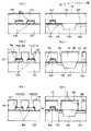
図3(a),(b)は図2(b)のAA線、BB線に沿う断面図であり、特に同図に示した第1配線層111に設けたコンタクトC11,C21を含む構造を示すものである。シリコン基板101の主面に設けられた素子分離絶縁膜105により前記N型拡散層102,P型拡散層103が区画形成されている。また、前記シリコン基板101の主面上にはゲート絶縁膜106を介してポリシリコン層104が形成され、前記各トランジスタQ1〜Q6のゲートを構成するゲート電極G1,G2,G3(ワード線WL)が形成されている。ここで、ゲート電極G1,G2,G3(ワード線WL)は、前記ポリシリコン層105の表面にTi(チタン)、Co(コバルト)等のシリサイド層107が形成されており、このシリサイド層107によってポリシリコン層104の低抵抗化が図られている。また、前記シリサイド層107は前記N型拡散層102及びP型拡散層103の表面にも形成されてこれらの低抵抗化が図られている。なお、実施例1ではポリシリコン層104の側壁には絶縁膜のサイドウォール108が形成されている。そして、全面に層間絶縁膜110が形成され、この層間絶縁膜110にコンタクトホール112が開口され、このコンタクトホール112により前記コンタクトCが形成されている。ここで、前記コンタクトホール112の内面にはTiN(窒化チタン)/Ti構造のバリアメタル層113が形成されるとともに、このバリアメタル層113内にW(タングステン)が埋設されてコンタクトプラグ114が形成されている。ここで、前記コンタクトホール112内では、その下層の前記ポリシリコン層104の表面に形成されているシリサイド層107はコンタクトホール112の底面において除去されており、前記バリアメタル層113は前記ポリシリコン層104に直接接続された構成となっている。そして、その上に形成されたアルミニウムからなる第1配線層111の一部によって前記ノード配線NL1,NL2が構成されている。 FIGS. 3A and 3B are cross-sectional views taken along lines AA and BB in FIG. 2B, and particularly have a structure including contacts C11 and C21 provided in the
図4は以上の構成のメモリセルを製造する方法を説明するための工程断面図であり、図3(a),(b)に対応する図である。先ず、図4(a1),(b1)に示すように、シリコン基板101に素子分離絶縁膜105を形成した後、当該シリコン基板101の全面にゲート酸化膜106を形成し、その上にポリシリコン層104を形成する。そして、前記ポリシリコン層104を選択的にパターニングしてゲート電極G1,G2,G3(ワード線WL)を形成し、続いてこれらのゲート電極の側面にサイドウォール108を形成した後、これらを利用した自己整合法によりシリコン基板101に不純物を注入してN型拡散層102とP型拡散層103を形成する。さらに、全面にTi,Coを積層し、かつ熱処理することでポリシリコン層104と拡散層102,103の表面にシリサイド層107を形成する。しかる上で、これらを覆うように層間絶縁膜110を形成する。 FIG. 4 is a process cross-sectional view for explaining a method of manufacturing the memory cell having the above-described structure, and corresponds to FIGS. 3 (a) and 3 (b). First, as shown in FIGS. 4A1 and 4B1, after an element
次いで、図4(a2),(b2)に示すように、前記層間絶縁膜110の所要箇所にコンタクトホール112を開口する。このコンタクトホール112は前記シリサイド層107に達するまで開口する。そして、図4(a3),(b3)に示すように、前記コンタクトC11,C21のコンタクトホール112を除く領域のコンタクトホール112をフォトレジストからなるレジストマスク131によって被覆した上で、被覆されていないコンタクトホール112(C11,C21)の底面に露呈しているシリサイド層107をドライエッチング又はウェットエッチング、もしくはドライエッチングとウェットエッチングを組み合わせた技術により自己整合的にエッチング除去する。これにより、コンタクトホール112(C11,C21)の底面においてのみシリサイド層107が除去され、この部分だけにポリシリコン層104が露呈されることになる。 Next, as shown in FIGS. 4A2 and 4B2, a
次いで、前記レジストマスク131を除去した後、図3(a),(b)に示したように、Ti/TiNをスパッタ技術等を用いて成膜してバリアメタル層113を形成し、さらに、CVD技術等を用いてコンタクトプラグを構成するW層114を成膜し、その後CMP(化学的機械研磨)技術もしくはエッチバック技術を用いて層間絶縁膜110上のこれらのW層114、バリアメタル層113を除去する。さらに、その上にアルミニウム層を形成し、これを所要のパターンにパターニングして第1配線層111を形成する。さらに、図示は省略するがその上に第2層間絶縁膜を形成し、コンタクトを介してアルミニウム膜による第2配線層121(図2(c)参照)を形成し、デジット線DL1,DL2をパターニングすることによりメモリセルMCが完成される。 Next, after removing the resist
以上のように製造された実施例1のメモリセルでは、各MOSトランジスタQ1〜Q4のゲート電極G1,G2は表面にシリサイド層107を有するポリシリコン層104で形成されるため、ゲート電極自体は低抵抗に構成できる。勿論ワード線WLとしてのMOSトランジスタQ5,Q6のゲート電極G3も同様であり、低抵抗に構成される。その一方で、当該ゲート電極G1,G2と対向する駆動トランジスタのドレインとを接続する第1配線層111からなるノード配線NL1,NL2は、W/TiN/Ti構造のコンタクトC11,C21において、シリサイド層107を介することなくポリシリコン層104に直接接続された構成となっている。そのため、このコンタクトC11,C21における第1配線層111とポリシリコン層104との接続構造は、シリサイド層107を介して接続している場合に比較してコンタクト抵抗が高くなり、結果として図1に示したようにノード配線NL1,NL2に高抵抗R1,R2を付加した等価回路が構成されることになる。前記付加抵抗R1,R2を接続しない配線の他のコンタクトCではコンタクトホール112の底面のシリサイド層107は除去されていないため、上層の配線層111とポリシリコン層104のコンタクト抵抗が低抵抗に構成できることは言うまでもない。 In the memory cell of the first embodiment manufactured as described above, the gate electrodes G1 and G2 of the MOS transistors Q1 to Q4 are formed of the
また、実施例1のメモリセルの製造方法では、層間絶縁膜110に開口したコンタクトホール112を利用した自己整合法によってポリシリコン層104上のシリサイド層107を除去すればよいので、特許文献1〜4のようにサリサイドを選択的に形成するための高精度のリソグラフィ工程が不要になり、容易に製造することができるようになる。特に、ポリシリコン層104上のシリサイド層107を選択的に除去するためにコンタクトホールを利用した自己整合法を利用することで、リソグラフィパターンにある程度のマージンを確保する必要はなく、メモリセルサイズが増大することもない。 Further, in the method of manufacturing the memory cell according to the first embodiment, the
実施例2は実施例1と製造工程の一部が相違しており、最終的に製造されるメモリセルの構造は実施例1とほぼ同じである。図5は実施例2の製造工程を示す図であり、実施例1の図4に対応する図である。先ず、図5(a1),(b1)に示すように、実施例1と同様に層間絶縁膜110を形成した後、当該層間絶縁膜110の表面にエッチングストッパ膜115を形成しておく。このエッチングストッパ膜115は後工程でシリサイド層107をエッチングする際に層間絶縁膜110の表面がダメージを受けないようにするためのものである。例えば、前記シリサイド層並びに層間膜に対して、エッチング選択比が高い材料を用いる。 The second embodiment is partially different from the first embodiment in the manufacturing process, and the structure of the finally manufactured memory cell is almost the same as that of the first embodiment. FIG. 5 is a diagram illustrating the manufacturing process of the second embodiment and corresponds to FIG. 4 of the first embodiment. First, as shown in FIGS. 5A1 and 5B1, an
しかる後、図5(a2),(b2)に示すように、前記エッチングストッパ膜115及び層間絶縁膜110を選択エッチングして所定の位置にコンタクトホール112を開口する。これにより、実施例1と同様に、コンタクトホール112の底面にのみシリサイド層を露出させることができる。しかる上で、図5(a3),(b3)に示すように、実施例1と同様に所定のコンタクトホール112を覆うレジストマスク131を形成し、このレジストマスク131並びにエッチングストッパ層115をマスクにドライエッチング又はウェットエッチング、もしくはドライエッチングとウェットエッチングを組み合わせた技術によりコンタクトホール112(C11,C21)の底面に露呈されているシリサイド層107を自己整合的に除去する。これにより、コンタクトホール112(C11,C21)の底面にポリシリコン層104が露出される。 Thereafter, as shown in FIGS. 5A2 and 5B2, the
以下の工程は実施例1と同様であり、図3(a),(b)に示したと同様のメモリセルを製造することができる。実施例2のメモリセルにおいても、各トランジスタのゲート電極G1,G2及びワード線WLとしてのゲート電極G3は表面にシリサイド層107を有するポリシリコン層104で形成されるため低抵抗に構成できる。その一方で、当該ゲート電極G1,G2と対向する駆動トランジスタQ3,Q4のドレインとを接続する第1配線層111からなるノード配線NL1,NL2はコンタクトC11,C21において、シリサイド層107を介することなくポリシリコン層104に直接接続された構成となっているので、このコンタクトC11,C21における第1配線層111とポリシリコン層104との接続はシリサイド層107を介して接続している場合に比較してコンタクト抵抗が高くなり、結果としてノード配線NL1,NL2に高抵抗R1,R2を付加することができ、図1の等価回路が構成されることになる。 The following steps are the same as those in the first embodiment, and the same memory cell as shown in FIGS. 3A and 3B can be manufactured. Also in the memory cell of the second embodiment, since the gate electrodes G1 and G2 of each transistor and the gate electrode G3 as the word line WL are formed of the
また、実施例2の製造方法でも、層間絶縁膜110に開口したコンタクトホール112を利用した自己整合法によってポリシリコン層104上のシリサイド層107を除去すればよいので、特許文献1〜4のようにサリサイドを選択的に形成するための高精度のリソグラフィ工程が不要になり、容易に製造することができるようになる。特に、ポリシリコン層104上のシリサイド層107を選択的に除去するためにコンタクトホールを利用した自己整合法を利用しているので、リソグラフィパターンにある程度のマージンを確保する必要はなく、メモリセルサイズが増大することもない。さらに実施例2では、層間絶縁膜110上に形成したエッチングストッパ膜115によってレジストマスク131で被覆されないコンタクトホール112(C11,C21)の周囲の層間絶縁膜に対するダメージが防止でき、当該層間絶縁膜110の表面を掘り下げることがなくなるので、コンタクト形状に異常をきたすことがなく、信頼性のあるコンタクトが得られる。 Also, in the manufacturing method of the second embodiment, the
本発明はSRAMのメモリセルの付加抵抗に適用されるのみではなく、ポリシリコン層上にシリサイド層を備えるサリサイド構造の配線に対して付加抵抗をコンタクト接続する構成であれば、当該コンタクトのコンタクトホールの底面のシリサイド層を自己整合的に除去するのみで本発明を適用することが可能である。 The present invention is not only applied to the additional resistance of the SRAM memory cell, but if the additional resistance is contact-connected to the wiring of the salicide structure having the silicide layer on the polysilicon layer, the contact hole of the contact is provided. The present invention can be applied only by removing the silicide layer on the bottom surface of the substrate in a self-aligned manner.
101 シリコン基板
102 N型拡散層
103 P型拡散層
104 ポリシリコン層
105 素子分離絶縁膜
106 ゲート絶縁膜
107 シリサイド層
108 サイドウォール
110 層間絶縁膜
111 第1配線層
112 コンタクトホール
113 バリアメタル層
114 コンタクトプラグ
115 エッチングストッパ膜
121 第2配線層
131 レジストマスク
Q1〜Q6 MOSトランジスタ
N1,N2 ノード
NL1,NL2 ノード配線
R1,R2 付加抵抗
C(C11,C21) コンタクト
MC メモリセル
G1,G2,G3 ゲート電極
WL ワード線
DL1,DL2 デジット線
101 Silicon substrate 102 N-type diffusion layer 103 P-
Claims (5)
Translated fromJapanesePriority Applications (3)
| Application Number | Priority Date | Filing Date | Title |
|---|---|---|---|
| JP2004095919AJP4566599B2 (en) | 2004-03-29 | 2004-03-29 | Semiconductor device and manufacturing method thereof |
| US11/085,201US20050212054A1 (en) | 2004-03-29 | 2005-03-22 | Semiconductor device and method of manufacturing the same |
| CNB2005100624576ACN100438042C (en) | 2004-03-29 | 2005-03-28 | Semiconductor device and method of manufacturing the same |
Applications Claiming Priority (1)
| Application Number | Priority Date | Filing Date | Title |
|---|---|---|---|
| JP2004095919AJP4566599B2 (en) | 2004-03-29 | 2004-03-29 | Semiconductor device and manufacturing method thereof |
Publications (2)
| Publication Number | Publication Date |
|---|---|
| JP2005285991A JP2005285991A (en) | 2005-10-13 |
| JP4566599B2true JP4566599B2 (en) | 2010-10-20 |
Family
ID=34988767
Family Applications (1)
| Application Number | Title | Priority Date | Filing Date |
|---|---|---|---|
| JP2004095919AExpired - Fee RelatedJP4566599B2 (en) | 2004-03-29 | 2004-03-29 | Semiconductor device and manufacturing method thereof |
Country Status (3)
| Country | Link |
|---|---|
| US (1) | US20050212054A1 (en) |
| JP (1) | JP4566599B2 (en) |
| CN (1) | CN100438042C (en) |
Families Citing this family (2)
| Publication number | Priority date | Publication date | Assignee | Title |
|---|---|---|---|---|
| US8188550B2 (en)* | 2007-12-27 | 2012-05-29 | Globalfoundries Singapore Pte. Ltd. | Integrated circuit structure with electrical strap and its method of forming |
| CN102157437B (en)* | 2010-02-11 | 2013-12-25 | 中国科学院微电子研究所 | Method for forming semiconductor structure |
Family Cites Families (16)
| Publication number | Priority date | Publication date | Assignee | Title |
|---|---|---|---|---|
| JPS63149536U (en)* | 1987-03-20 | 1988-10-03 | ||
| JPH02129915A (en)* | 1988-11-09 | 1990-05-18 | Seiko Instr Inc | Manufacture of mos semiconductor device |
| JP2555755B2 (en)* | 1990-04-20 | 1996-11-20 | 三菱電機株式会社 | Semiconductor device and manufacturing method thereof |
| JP2798321B2 (en)* | 1991-03-06 | 1998-09-17 | 三菱電機株式会社 | Method for manufacturing semiconductor device |
| JPH06283612A (en)* | 1993-03-26 | 1994-10-07 | Mitsubishi Electric Corp | Semiconductor device and manufacture of semiconductor device |
| US5547892A (en)* | 1995-04-27 | 1996-08-20 | Taiwan Semiconductor Manufacturing Company | Process for forming stacked contacts and metal contacts on static random access memory having thin film transistors |
| JP2000306860A (en)* | 1999-04-20 | 2000-11-02 | Nec Corp | Manufacture of semiconductor device |
| JP3921331B2 (en)* | 2000-05-26 | 2007-05-30 | 富士通株式会社 | Semiconductor device |
| JP2003060087A (en)* | 2001-08-10 | 2003-02-28 | Mitsubishi Electric Corp | Semiconductor storage device |
| JP2003133525A (en)* | 2001-10-23 | 2003-05-09 | Sharp Corp | Semiconductor memory device and method of manufacturing the same |
| US6670642B2 (en)* | 2002-01-22 | 2003-12-30 | Renesas Technology Corporation. | Semiconductor memory device using vertical-channel transistors |
| JP2004013920A (en)* | 2002-06-03 | 2004-01-15 | Mitsubishi Electric Corp | Semiconductor storage device |
| JP2004200385A (en)* | 2002-12-18 | 2004-07-15 | Renesas Technology Corp | Semiconductor device and manufacturing method thereof |
| US6982451B1 (en)* | 2003-03-27 | 2006-01-03 | Xilinx, Inc. | Single event upset in SRAM cells in FPGAs with high resistivity gate structures |
| JP2005026273A (en)* | 2003-06-30 | 2005-01-27 | Fujitsu Ltd | Semiconductor device and manufacturing method thereof |
| JP2005217246A (en)* | 2004-01-30 | 2005-08-11 | Toshiba Corp | Semiconductor device |
- 2004
- 2004-03-29JPJP2004095919Apatent/JP4566599B2/ennot_activeExpired - Fee Related
- 2005
- 2005-03-22USUS11/085,201patent/US20050212054A1/ennot_activeAbandoned
- 2005-03-28CNCNB2005100624576Apatent/CN100438042C/ennot_activeExpired - Fee Related
Also Published As
| Publication number | Publication date |
|---|---|
| US20050212054A1 (en) | 2005-09-29 |
| CN1677677A (en) | 2005-10-05 |
| CN100438042C (en) | 2008-11-26 |
| JP2005285991A (en) | 2005-10-13 |
Similar Documents
| Publication | Publication Date | Title |
|---|---|---|
| US8138048B2 (en) | Semiconductor storage device | |
| JP2524862B2 (en) | Semiconductor memory device and manufacturing method thereof | |
| US6420227B1 (en) | Semiconductor integrated circuit device and process for manufacture of the same | |
| US20060091468A1 (en) | Top and sidewall bridged interconnect structure and method | |
| US6300229B1 (en) | Semiconductor device and method of manufacturing the same | |
| US9040403B2 (en) | Methods for fabricating integrated circuits having gate to active and gate to gate interconnects | |
| US8946821B2 (en) | SRAM integrated circuits and methods for their fabrication | |
| JPH0828473B2 (en) | Semiconductor device and manufacturing method thereof | |
| JP2002289703A (en) | Semiconductor memory and its manufacturing method | |
| US6437455B2 (en) | Semiconductor device having gate-gate, drain-drain, and drain-gate connecting layers and method of fabricating the same | |
| JPH0794595A (en) | Semiconductor device and manufacturing method thereof | |
| JP2923912B2 (en) | Semiconductor device | |
| JPH0766297A (en) | Semiconductor memory device | |
| US6404023B1 (en) | Semiconductor device having gate-gate, drain-drain, and drain-gate connecting layers and method of fabricating the same | |
| US6534864B1 (en) | Semiconductor memory device and method of fabricating the same | |
| US7078774B2 (en) | Semiconductor memory device having a shallow trench isolation structure | |
| JP4566599B2 (en) | Semiconductor device and manufacturing method thereof | |
| JP2008235793A (en) | Semiconductor device and manufacturing method thereof | |
| JPH09162370A (en) | Semiconductor integrated circuit device and method of manufacturing the same | |
| US6376298B1 (en) | Layout method for scalable design of the aggressive RAM cells using a poly-cap mask | |
| JP3436462B2 (en) | Semiconductor device | |
| US5290728A (en) | Method for producing a semiconductor device | |
| US7714395B2 (en) | Static random access memory and fabricating method thereof | |
| JPH0992731A (en) | Semiconductor device having LDD transistor | |
| JP2877069B2 (en) | Static semiconductor memory device |
Legal Events
| Date | Code | Title | Description |
|---|---|---|---|
| A621 | Written request for application examination | Free format text:JAPANESE INTERMEDIATE CODE: A621 Effective date:20070206 | |
| A977 | Report on retrieval | Free format text:JAPANESE INTERMEDIATE CODE: A971007 Effective date:20090930 | |
| A131 | Notification of reasons for refusal | Free format text:JAPANESE INTERMEDIATE CODE: A131 Effective date:20091013 | |
| A521 | Request for written amendment filed | Free format text:JAPANESE INTERMEDIATE CODE: A523 Effective date:20091210 | |
| RD01 | Notification of change of attorney | Free format text:JAPANESE INTERMEDIATE CODE: A7421 Effective date:20100623 | |
| TRDD | Decision of grant or rejection written | ||
| A01 | Written decision to grant a patent or to grant a registration (utility model) | Free format text:JAPANESE INTERMEDIATE CODE: A01 Effective date:20100803 | |
| A01 | Written decision to grant a patent or to grant a registration (utility model) | Free format text:JAPANESE INTERMEDIATE CODE: A01 | |
| A61 | First payment of annual fees (during grant procedure) | Free format text:JAPANESE INTERMEDIATE CODE: A61 Effective date:20100804 | |
| R150 | Certificate of patent or registration of utility model | Free format text:JAPANESE INTERMEDIATE CODE: R150 | |
| FPAY | Renewal fee payment (event date is renewal date of database) | Free format text:PAYMENT UNTIL: 20130813 Year of fee payment:3 | |
| LAPS | Cancellation because of no payment of annual fees |