JP4564342B2 - Multilayer wiring board and manufacturing method thereof - Google Patents
Multilayer wiring board and manufacturing method thereofDownload PDFInfo
- Publication number
- JP4564342B2 JP4564342B2JP2004338490AJP2004338490AJP4564342B2JP 4564342 B2JP4564342 B2JP 4564342B2JP 2004338490 AJP2004338490 AJP 2004338490AJP 2004338490 AJP2004338490 AJP 2004338490AJP 4564342 B2JP4564342 B2JP 4564342B2
- Authority
- JP
- Japan
- Prior art keywords
- insulating film
- layer
- conductive material
- wiring board
- conductive
- Prior art date
- Legal status (The legal status is an assumption and is not a legal conclusion. Google has not performed a legal analysis and makes no representation as to the accuracy of the status listed.)
- Expired - Fee Related
Links
Images


Classifications
- H—ELECTRICITY
- H05—ELECTRIC TECHNIQUES NOT OTHERWISE PROVIDED FOR
- H05K—PRINTED CIRCUITS; CASINGS OR CONSTRUCTIONAL DETAILS OF ELECTRIC APPARATUS; MANUFACTURE OF ASSEMBLAGES OF ELECTRICAL COMPONENTS
- H05K3/00—Apparatus or processes for manufacturing printed circuits
- H05K3/46—Manufacturing multilayer circuits
- H—ELECTRICITY
- H05—ELECTRIC TECHNIQUES NOT OTHERWISE PROVIDED FOR
- H05K—PRINTED CIRCUITS; CASINGS OR CONSTRUCTIONAL DETAILS OF ELECTRIC APPARATUS; MANUFACTURE OF ASSEMBLAGES OF ELECTRICAL COMPONENTS
- H05K3/00—Apparatus or processes for manufacturing printed circuits
- H05K3/40—Forming printed elements for providing electric connections to or between printed circuits
- H05K3/4038—Through-connections; Vertical interconnect access [VIA] connections
- H05K3/4076—Through-connections; Vertical interconnect access [VIA] connections by thin-film techniques
- C—CHEMISTRY; METALLURGY
- C23—COATING METALLIC MATERIAL; COATING MATERIAL WITH METALLIC MATERIAL; CHEMICAL SURFACE TREATMENT; DIFFUSION TREATMENT OF METALLIC MATERIAL; COATING BY VACUUM EVAPORATION, BY SPUTTERING, BY ION IMPLANTATION OR BY CHEMICAL VAPOUR DEPOSITION, IN GENERAL; INHIBITING CORROSION OF METALLIC MATERIAL OR INCRUSTATION IN GENERAL
- C23C—COATING METALLIC MATERIAL; COATING MATERIAL WITH METALLIC MATERIAL; SURFACE TREATMENT OF METALLIC MATERIAL BY DIFFUSION INTO THE SURFACE, BY CHEMICAL CONVERSION OR SUBSTITUTION; COATING BY VACUUM EVAPORATION, BY SPUTTERING, BY ION IMPLANTATION OR BY CHEMICAL VAPOUR DEPOSITION, IN GENERAL
- C23C16/00—Chemical coating by decomposition of gaseous compounds, without leaving reaction products of surface material in the coating, i.e. chemical vapour deposition [CVD] processes
- C23C16/02—Pretreatment of the material to be coated
- C23C16/0227—Pretreatment of the material to be coated by cleaning or etching
- C23C16/0245—Pretreatment of the material to be coated by cleaning or etching by etching with a plasma
- C—CHEMISTRY; METALLURGY
- C23—COATING METALLIC MATERIAL; COATING MATERIAL WITH METALLIC MATERIAL; CHEMICAL SURFACE TREATMENT; DIFFUSION TREATMENT OF METALLIC MATERIAL; COATING BY VACUUM EVAPORATION, BY SPUTTERING, BY ION IMPLANTATION OR BY CHEMICAL VAPOUR DEPOSITION, IN GENERAL; INHIBITING CORROSION OF METALLIC MATERIAL OR INCRUSTATION IN GENERAL
- C23C—COATING METALLIC MATERIAL; COATING MATERIAL WITH METALLIC MATERIAL; SURFACE TREATMENT OF METALLIC MATERIAL BY DIFFUSION INTO THE SURFACE, BY CHEMICAL CONVERSION OR SUBSTITUTION; COATING BY VACUUM EVAPORATION, BY SPUTTERING, BY ION IMPLANTATION OR BY CHEMICAL VAPOUR DEPOSITION, IN GENERAL
- C23C16/00—Chemical coating by decomposition of gaseous compounds, without leaving reaction products of surface material in the coating, i.e. chemical vapour deposition [CVD] processes
- C23C16/06—Chemical coating by decomposition of gaseous compounds, without leaving reaction products of surface material in the coating, i.e. chemical vapour deposition [CVD] processes characterised by the deposition of metallic material
- C23C16/18—Chemical coating by decomposition of gaseous compounds, without leaving reaction products of surface material in the coating, i.e. chemical vapour deposition [CVD] processes characterised by the deposition of metallic material from metallo-organic compounds
- H—ELECTRICITY
- H01—ELECTRIC ELEMENTS
- H01L—SEMICONDUCTOR DEVICES NOT COVERED BY CLASS H10
- H01L21/00—Processes or apparatus adapted for the manufacture or treatment of semiconductor or solid state devices or of parts thereof
- H01L21/02—Manufacture or treatment of semiconductor devices or of parts thereof
- H01L21/04—Manufacture or treatment of semiconductor devices or of parts thereof the devices having potential barriers, e.g. a PN junction, depletion layer or carrier concentration layer
- H01L21/48—Manufacture or treatment of parts, e.g. containers, prior to assembly of the devices, using processes not provided for in a single one of the groups H01L21/18 - H01L21/326 or H10D48/04 - H10D48/07
- H01L21/4814—Conductive parts
- H01L21/4846—Leads on or in insulating or insulated substrates, e.g. metallisation
- H01L21/486—Via connections through the substrate with or without pins
- H—ELECTRICITY
- H01—ELECTRIC ELEMENTS
- H01L—SEMICONDUCTOR DEVICES NOT COVERED BY CLASS H10
- H01L23/00—Details of semiconductor or other solid state devices
- H01L23/48—Arrangements for conducting electric current to or from the solid state body in operation, e.g. leads, terminal arrangements ; Selection of materials therefor
- H01L23/488—Arrangements for conducting electric current to or from the solid state body in operation, e.g. leads, terminal arrangements ; Selection of materials therefor consisting of soldered or bonded constructions
- H01L23/498—Leads, i.e. metallisations or lead-frames on insulating substrates, e.g. chip carriers
- H01L23/49827—Via connections through the substrates, e.g. pins going through the substrate, coaxial cables
- H—ELECTRICITY
- H05—ELECTRIC TECHNIQUES NOT OTHERWISE PROVIDED FOR
- H05K—PRINTED CIRCUITS; CASINGS OR CONSTRUCTIONAL DETAILS OF ELECTRIC APPARATUS; MANUFACTURE OF ASSEMBLAGES OF ELECTRICAL COMPONENTS
- H05K3/00—Apparatus or processes for manufacturing printed circuits
- H05K3/0011—Working of insulating substrates or insulating layers
- H05K3/0017—Etching of the substrate by chemical or physical means
- H05K3/0041—Etching of the substrate by chemical or physical means by plasma etching
- H—ELECTRICITY
- H05—ELECTRIC TECHNIQUES NOT OTHERWISE PROVIDED FOR
- H05K—PRINTED CIRCUITS; CASINGS OR CONSTRUCTIONAL DETAILS OF ELECTRIC APPARATUS; MANUFACTURE OF ASSEMBLAGES OF ELECTRICAL COMPONENTS
- H05K3/00—Apparatus or processes for manufacturing printed circuits
- H05K3/0073—Masks not provided for in groups H05K3/02 - H05K3/46, e.g. for photomechanical production of patterned surfaces
- H05K3/0079—Masks not provided for in groups H05K3/02 - H05K3/46, e.g. for photomechanical production of patterned surfaces characterised by the method of application or removal of the mask
- H—ELECTRICITY
- H05—ELECTRIC TECHNIQUES NOT OTHERWISE PROVIDED FOR
- H05K—PRINTED CIRCUITS; CASINGS OR CONSTRUCTIONAL DETAILS OF ELECTRIC APPARATUS; MANUFACTURE OF ASSEMBLAGES OF ELECTRICAL COMPONENTS
- H05K3/00—Apparatus or processes for manufacturing printed circuits
- H05K3/40—Forming printed elements for providing electric connections to or between printed circuits
- H05K3/42—Plated through-holes or plated via connections
- H05K3/423—Plated through-holes or plated via connections characterised by electroplating method
- H—ELECTRICITY
- H05—ELECTRIC TECHNIQUES NOT OTHERWISE PROVIDED FOR
- H05K—PRINTED CIRCUITS; CASINGS OR CONSTRUCTIONAL DETAILS OF ELECTRIC APPARATUS; MANUFACTURE OF ASSEMBLAGES OF ELECTRICAL COMPONENTS
- H05K3/00—Apparatus or processes for manufacturing printed circuits
- H05K3/44—Manufacturing insulated metal core circuits or other insulated electrically conductive core circuits
- H05K3/445—Manufacturing insulated metal core circuits or other insulated electrically conductive core circuits having insulated holes or insulated via connections through the metal core
- H—ELECTRICITY
- H05—ELECTRIC TECHNIQUES NOT OTHERWISE PROVIDED FOR
- H05K—PRINTED CIRCUITS; CASINGS OR CONSTRUCTIONAL DETAILS OF ELECTRIC APPARATUS; MANUFACTURE OF ASSEMBLAGES OF ELECTRICAL COMPONENTS
- H05K3/00—Apparatus or processes for manufacturing printed circuits
- H05K3/46—Manufacturing multilayer circuits
- H05K3/4602—Manufacturing multilayer circuits characterized by a special circuit board as base or central core whereon additional circuit layers are built or additional circuit boards are laminated
- H05K3/4605—Manufacturing multilayer circuits characterized by a special circuit board as base or central core whereon additional circuit layers are built or additional circuit boards are laminated made from inorganic insulating material
- H—ELECTRICITY
- H05—ELECTRIC TECHNIQUES NOT OTHERWISE PROVIDED FOR
- H05K—PRINTED CIRCUITS; CASINGS OR CONSTRUCTIONAL DETAILS OF ELECTRIC APPARATUS; MANUFACTURE OF ASSEMBLAGES OF ELECTRICAL COMPONENTS
- H05K3/00—Apparatus or processes for manufacturing printed circuits
- H05K3/46—Manufacturing multilayer circuits
- H05K3/4644—Manufacturing multilayer circuits by building the multilayer layer by layer, i.e. build-up multilayer circuits
- H05K3/4679—Aligning added circuit layers or via connections relative to previous circuit layers
- H—ELECTRICITY
- H01—ELECTRIC ELEMENTS
- H01L—SEMICONDUCTOR DEVICES NOT COVERED BY CLASS H10
- H01L21/00—Processes or apparatus adapted for the manufacture or treatment of semiconductor or solid state devices or of parts thereof
- H01L21/67—Apparatus specially adapted for handling semiconductor or electric solid state devices during manufacture or treatment thereof; Apparatus specially adapted for handling wafers during manufacture or treatment of semiconductor or electric solid state devices or components ; Apparatus not specifically provided for elsewhere
- H01L21/683—Apparatus specially adapted for handling semiconductor or electric solid state devices during manufacture or treatment thereof; Apparatus specially adapted for handling wafers during manufacture or treatment of semiconductor or electric solid state devices or components ; Apparatus not specifically provided for elsewhere for supporting or gripping
- H01L21/6835—Apparatus specially adapted for handling semiconductor or electric solid state devices during manufacture or treatment thereof; Apparatus specially adapted for handling wafers during manufacture or treatment of semiconductor or electric solid state devices or components ; Apparatus not specifically provided for elsewhere for supporting or gripping using temporarily an auxiliary support
- H—ELECTRICITY
- H01—ELECTRIC ELEMENTS
- H01L—SEMICONDUCTOR DEVICES NOT COVERED BY CLASS H10
- H01L2924/00—Indexing scheme for arrangements or methods for connecting or disconnecting semiconductor or solid-state bodies as covered by H01L24/00
- H01L2924/0001—Technical content checked by a classifier
- H01L2924/0002—Not covered by any one of groups H01L24/00, H01L24/00 and H01L2224/00
- H—ELECTRICITY
- H05—ELECTRIC TECHNIQUES NOT OTHERWISE PROVIDED FOR
- H05K—PRINTED CIRCUITS; CASINGS OR CONSTRUCTIONAL DETAILS OF ELECTRIC APPARATUS; MANUFACTURE OF ASSEMBLAGES OF ELECTRICAL COMPONENTS
- H05K1/00—Printed circuits
- H05K1/02—Details
- H05K1/03—Use of materials for the substrate
- H05K1/0306—Inorganic insulating substrates, e.g. ceramic, glass
- H—ELECTRICITY
- H05—ELECTRIC TECHNIQUES NOT OTHERWISE PROVIDED FOR
- H05K—PRINTED CIRCUITS; CASINGS OR CONSTRUCTIONAL DETAILS OF ELECTRIC APPARATUS; MANUFACTURE OF ASSEMBLAGES OF ELECTRICAL COMPONENTS
- H05K2201/00—Indexing scheme relating to printed circuits covered by H05K1/00
- H05K2201/09—Shape and layout
- H05K2201/09209—Shape and layout details of conductors
- H05K2201/095—Conductive through-holes or vias
- H05K2201/09563—Metal filled via
- H—ELECTRICITY
- H05—ELECTRIC TECHNIQUES NOT OTHERWISE PROVIDED FOR
- H05K—PRINTED CIRCUITS; CASINGS OR CONSTRUCTIONAL DETAILS OF ELECTRIC APPARATUS; MANUFACTURE OF ASSEMBLAGES OF ELECTRICAL COMPONENTS
- H05K2201/00—Indexing scheme relating to printed circuits covered by H05K1/00
- H05K2201/09—Shape and layout
- H05K2201/09209—Shape and layout details of conductors
- H05K2201/095—Conductive through-holes or vias
- H05K2201/096—Vertically aligned vias, holes or stacked vias
- H—ELECTRICITY
- H05—ELECTRIC TECHNIQUES NOT OTHERWISE PROVIDED FOR
- H05K—PRINTED CIRCUITS; CASINGS OR CONSTRUCTIONAL DETAILS OF ELECTRIC APPARATUS; MANUFACTURE OF ASSEMBLAGES OF ELECTRICAL COMPONENTS
- H05K2203/00—Indexing scheme relating to apparatus or processes for manufacturing printed circuits covered by H05K3/00
- H05K2203/09—Treatments involving charged particles
- H05K2203/095—Plasma, e.g. for treating a substrate to improve adhesion with a conductor or for cleaning holes
- H—ELECTRICITY
- H05—ELECTRIC TECHNIQUES NOT OTHERWISE PROVIDED FOR
- H05K—PRINTED CIRCUITS; CASINGS OR CONSTRUCTIONAL DETAILS OF ELECTRIC APPARATUS; MANUFACTURE OF ASSEMBLAGES OF ELECTRICAL COMPONENTS
- H05K3/00—Apparatus or processes for manufacturing printed circuits
- H05K3/38—Improvement of the adhesion between the insulating substrate and the metal
- H05K3/388—Improvement of the adhesion between the insulating substrate and the metal by the use of a metallic or inorganic thin film adhesion layer
- Y—GENERAL TAGGING OF NEW TECHNOLOGICAL DEVELOPMENTS; GENERAL TAGGING OF CROSS-SECTIONAL TECHNOLOGIES SPANNING OVER SEVERAL SECTIONS OF THE IPC; TECHNICAL SUBJECTS COVERED BY FORMER USPC CROSS-REFERENCE ART COLLECTIONS [XRACs] AND DIGESTS
- Y10—TECHNICAL SUBJECTS COVERED BY FORMER USPC
- Y10T—TECHNICAL SUBJECTS COVERED BY FORMER US CLASSIFICATION
- Y10T29/00—Metal working
- Y10T29/49—Method of mechanical manufacture
- Y10T29/49002—Electrical device making
- Y10T29/49117—Conductor or circuit manufacturing
- Y10T29/49124—On flat or curved insulated base, e.g., printed circuit, etc.
- Y10T29/49155—Manufacturing circuit on or in base
Landscapes
- Engineering & Computer Science (AREA)
- Microelectronics & Electronic Packaging (AREA)
- Manufacturing & Machinery (AREA)
- Chemical & Material Sciences (AREA)
- Physics & Mathematics (AREA)
- Condensed Matter Physics & Semiconductors (AREA)
- General Physics & Mathematics (AREA)
- Computer Hardware Design (AREA)
- Power Engineering (AREA)
- Mechanical Engineering (AREA)
- General Chemical & Material Sciences (AREA)
- Chemical Kinetics & Catalysis (AREA)
- Materials Engineering (AREA)
- Plasma & Fusion (AREA)
- Metallurgy (AREA)
- Organic Chemistry (AREA)
- Ceramic Engineering (AREA)
- Inorganic Chemistry (AREA)
- Production Of Multi-Layered Print Wiring Board (AREA)
- Internal Circuitry In Semiconductor Integrated Circuit Devices (AREA)
- Printing Elements For Providing Electric Connections Between Printed Circuits (AREA)
Description
Translated fromJapanese本発明は、多層配線基板とその製造方法に係り、特に半導体チップを搭載するための高密度配線がなされた多層配線基板と、このような多層配線基板を製造するための製造方法に関する。 The present invention relates to a multilayer wiring board and a manufacturing method thereof, and more particularly to a multilayer wiring board on which high-density wiring for mounting a semiconductor chip is made and a manufacturing method for manufacturing such a multilayer wiring board.
近年、電子機器の高機能化、小型化、軽量化が進む中で、半導体パッケージの小型化、多ピン化、外部端子のファインピッチ化が求められており、高密度配線基板の要求がますます強くなっている。このため、LSIを直接プリント配線基板に実装したり、あるいはCSP(Chip Size Package)、BGA(Ball grid Array)をプリント配線基板に実装するようになってきた。そして、プリント配線基板も高密度化に対応するために、配線およびビアを1層づつ電気絶縁層を介してコア基板に多層に積み上げていくビルドアップ法で製作した多層配線基板を使用するようになってきた。 In recent years, as electronic devices become more sophisticated, smaller, and lighter, semiconductor packages are required to be smaller, have more pins, and have finer pitches for external terminals, and there is an increasing demand for high-density wiring boards. It is getting stronger. For this reason, LSIs are directly mounted on a printed wiring board, or CSP (Chip Size Package) and BGA (Ball grid Array) are mounted on a printed wiring board. In order to cope with the higher density of the printed wiring board, a multilayer wiring board manufactured by a build-up method in which wiring and vias are stacked in layers on the core board through an electric insulating layer one by one is used. It has become.
従来の一般的なビルドアップ多層配線基板では、絶縁基板にドリルでスルーホールを設け、このスルーホール内側に金属めっきを施し、スルーホール内に樹脂または導電性ペーストを充填して形成されたコア基板が使用されていた(特許文献1)。このコア基板は、スルーホールを介して表裏が導通されたものであり、このコア基板上に配線を電気絶縁層を介して多層に積み上げることで多層配線基板が作製されていた。また、最近では、樹脂を充填したスルーホールに蓋めっき(スルーホールの開口部分を塞ぐようにめっき層を形成すること)を行い、上記の蓋めっき部分の直上にビアを配置し、さらに、このビア上にビアを配置するスタック構造の多層配線基板が開発されている(特許文献2)。
しかし、従来のスルーホールの形成はドリル加工で行っていたため、スルーホールの開口径はドリル径よりも小さくすることができず、微細なドリルを用いたドリル加工では、ドリルの破損頻度が高いものであった。このため、スルーホールの微細化が困難であり、配線設計の自由度が限定されるという問題があった。
また、樹脂を充填したスルーホールに蓋めっきを行った構造では、使用する絶縁基板の熱収縮・熱膨張によって、スルーホール内部に充填した樹脂が伸縮し、これにより、蓋めっき部分に形成されたビアに応力が集中し易く、接続信頼性が低いという問題もあった。
本発明は、上記のような実情に鑑みてなされたものであり、配線設計の自由度が高く高密度配線が可能な多層配線基板と、このような多層配線基板を簡便に製造するための製造方法を提供することを目的とする。However, since conventional through-hole formation was performed by drilling, the through-hole opening diameter cannot be made smaller than the drill diameter, and drilling with a fine drill has a high frequency of breakage. Met. For this reason, there is a problem that it is difficult to miniaturize the through hole and the degree of freedom in wiring design is limited.
In addition, in the structure in which the through hole filled with resin is plated with lid, the resin filled inside the through hole expands and contracts due to the thermal contraction and thermal expansion of the insulating substrate to be used, thereby forming the lid plating part. There is also a problem that stress is easily concentrated on the via and connection reliability is low.
The present invention has been made in view of the above circumstances, and has a multilayer wiring board capable of high-density wiring with a high degree of freedom in wiring design, and manufacturing for easily manufacturing such a multilayer wiring board. It aims to provide a method.
このような目的を達成するために、本発明は、コア基板上に電気絶縁層を介して2層以上の配線を有する多層配線基板において、コア基板はシリコンコア基板であり、導電性物質が充填され表裏の導通がなされた複数のスルーホールを備え、前記スルーホールは開口径が10〜100μmの範囲内であり、前記スルーホール内壁面に第1の絶縁膜、導電性物質拡散防止層、第2の絶縁膜がこの順に積層されており、第1の絶縁膜はシリコンコア基板の熱酸化により形成した酸化珪素膜であり、前記第2の絶縁膜を介して導電性物質が前記スルーホール内に充填されており、電気絶縁層を介してコア基板上に形成された1層目の配線は、前記スルーホール内の前記導電性物質にビアを介して接続されているような構成とした。
本発明の好ましい態様として、第2の絶縁膜は、二酸化珪素薄膜であるような構成とした。In order to achieve such an object, the present invention provides a multilayer wiring board having two or more wirings on an electric insulating layer on a core board. The core board is asilicon core board and is filled witha conductive material. A plurality of through holes that are electrically connected to each other, the through holes having an opening diameter within a range of 10 to 100 μm, and afirst insulating film, a conductive material diffusion preventing layer, Two insulating films are laminated in this order, andthe first insulating film is a silicon oxide film formed by thermal oxidation of the silicon core substrate, and the conductive material is placed in the through-holes viathe second insulating film. The first-layer wiring formed on the core substrate via the electrical insulating layer is connected to the conductive substance in the through hole via a via.
As a preferred aspect of the present invention, the second insulating film is a silicon dioxide thin film.
本発明は、コア基板上に電気絶縁層を介して2層以上の配線を有する多層配線基板において、コア基板はシリコンコア基板であり、導電性物質が充填され表裏の導通がなされた複数のスルーホールを備え、前記スルーホールは開口径が10〜100μmの範囲内であり、前記スルーホール内壁面に第1の絶縁膜、第2の絶縁層、導電性物質拡散防止層、第3の絶縁膜がこの順に積層されており、第1の絶縁膜はシリコンコア基板の熱酸化により形成した酸化珪素膜であり、第2の絶縁膜と第3の絶縁膜の成分が同じであり、前記第3の絶縁膜を介して導電性物質が前記スルーホール内に充填されており、電気絶縁層を介してコア基板上に形成された1層目の配線は、前記スルーホール内の前記導電性物質にビアを介して接続されているような構成とした。
本発明の好ましい態様として、第2の絶縁膜、第3の絶縁膜は、二酸化珪素薄膜であるような構成とした。The present invention relatesto a multilayer wiring board having two or more layers of wirings on an electric insulating layer on a core substrate, wherein the core substrate is a silicon core substrate, and a plurality of through-holes filled with a conductive material and made conductive on the front and back sides. A through hole having an opening diameter in a range of 10 to 100 μm, and a first insulating film, a second insulating layer, a conductive material diffusion preventing layer, and a third insulating film on an inner wall surface of the through hole. Are stacked in this order, and the first insulating film is a silicon oxide film formed by thermal oxidation of the silicon core substrate, and the components of the second insulating film and the third insulating film are the same. The through hole is filled with a conductive material through the insulating film, and the first layer wiring formed on the core substrate through the electrical insulating layer is connected to the conductive material in the through hole. Like connected via It was formed.
As a preferred embodiment of the present invention,the second insulating film and the third insulating film are configured to be silicon dioxide thin films.
本発明の好ましい態様として、前記導電性物質拡散防止層は、窒化チタン薄膜であるような構成とした。
本発明の好ましい態様として、前記導電性物質は、電解めっきによりスルーホール内に形成された銅であるような構成とした。As a preferred embodiment of the present invention, theconductive substance diffusion prevention layer is configured to be atitanium nitride thin film .
As a preferred aspect of the present invention, the conductive material is configured to be copper formed in the through hole by electrolytic plating.
本発明の好ましい態様として、前記導電性物質は、スルーホール内に充填された導電性ペーストであるような構成とした。
本発明の好ましい態様として、前記スルーホールの開口径は、10〜70μmの範囲内であるような構成とした。
本発明の好ましい態様として、前記コア基板の厚みは、50〜725μmの範囲内であるような構成とした。As a preferred aspect of the present invention, the conductive substance is configured to be a conductive paste filled in a through hole.
As a preferred embodiment of the present invention, the opening diameter of the through hole is in the range of 10 to 70 μm.
As a preferred aspect of the present invention, the core substrate has a thickness in the range of 50 to 725 μm.
また、本発明は、コア基板上に電気絶縁層を介して2層以上の配線を有する多層配線基板の製造方法において、コア基板用のシリコンコア材の一方の面から、プラズマを利用したドライエッチングにより開口径が10〜100μmの範囲内にある微細孔を所定の深さまで穿設する工程と、前記微細孔の内壁面を含むシリコンコア材表面に、導電性物質拡散防止層が絶縁膜で被覆されるように絶縁膜および導電性物質拡散防止層を形成し、その後、少なくとも微細孔の内壁面に位置する絶縁膜上に下地導電層を形成する工程と、前記微細孔内を除く前記シリコンコア材上に所望のレジスト膜を形成し、前記下地導電層を給電層として前記微細孔内に電解めっきにより導電性物質を充填する工程と、前記レジスト膜を除去し、前記シリコンコア材の他方の面を研磨して前記微細孔を露出させることによりスルーホールを形成し、前記導電性物質によりスルーホールを介した表裏の導通がとられたシリコンコア基板とする工程と、該シリコンコア基板上に、スルーホール内に充填された導電性物質に接続するようにビアを形成すると同時に、電気絶縁層を介した1層目の配線を形成する工程と、を有し、絶縁膜および導電性物質拡散防止層を形成する工程では、第1の絶縁膜、導電性物質拡散防止層、第2の絶縁膜の順に積層する方法、第1の絶縁膜、第2の絶縁膜、導電性物質拡散防止層、第3の絶縁膜の順に積層する方法のいずれかを用いて絶縁膜および導電性物質拡散防止層を形成し、前記第1の絶縁膜の形成は、シリコンコア基板の熱酸化を利用して行うような構成とした。
本発明の好ましい態様として、前記下地導電層の形成は、MO−CVD法により行うような構成とした。The present invention also provides a dry etching process using plasma from one surface of asilicon core material for a core substrate in a method for manufacturing a multilayer wiring substrate having two or more layers of wirings on an electrical insulating layer on a core substrate. A step of drilling micropores having an opening diameter in the range of 10 to 100 μm to a predetermined depth and a surface of thesilicon core material including the inner wall surface of the micropores covered with a conductive substance diffusion prevention layer with an insulating film Forming an insulating film and a conductive material diffusion preventing layer, and then forming a base conductive layer on at least the insulating film located on the inner wall surface of the micropore, and thesilicon core excluding the micropore forming a desired resist film on wood, said a step of filling a conductive material by electrolytic plating in said micropores electroconductive base layer as a feeding layer, removing the resist film, thesilicon core material A step of polishing the other surface of the through-hole is formed by exposing the micropores, the front and backsilicon core substrate conduction was taken in through the through hole by the conductive material, thesilicon core substrate above, at the same time to form a via to connect the conductive material filled in the through holes,and perforated and forming a first wiring layer through an electrical insulating layer, theinsulating film and the conductive In the step of forming the material diffusion preventing layer, the first insulating film, the conductive material diffusion preventing layer, the method of laminating the second insulating film in this order, the first insulating film, the second insulating film, and the conductive material diffusion An insulating film and a conductive material diffusion preventing layer are formed using any one of the methods of laminating the preventing layer and the third insulating film in this order, and the formation of the first insulating film uses thermal oxidation of the silicon core substrate It wasthen, such ascarried out by configuration.
As a preferred embodiment of the present invention, the base conductive layer is formed by MO-CVD.
また、本発明は、コア基板上に電気絶縁層を介して2層以上の配線を有する多層配線基板の製造方法において、コア基板用のシリコンコア材の一方の面から、プラズマを利用したドライエッチングにより開口径が10〜100μmの範囲内にある微細孔を所定の深さまで穿設する工程と、前記シリコンコア材の他方の面を研磨して前記微細孔を露出させスルーホールを形成する工程と、少なくとも前記スルーホールの内壁面に、導電性物質拡散防止層が絶縁膜で被覆されるように絶縁膜および導電性物質拡散防止層を形成する工程と、前記スルーホール内に導電性物質を充填して表裏の導通がとられたシリコンコア基板とする工程と、該シリコンコア基板上に、スルーホール内に充填された導電性物質に接続するようにビアを形成すると同時に、電気絶縁層を介した1層目の配線を形成する工程と、を有し、絶縁膜および導電性物質拡散防止層を形成する工程では、第1の絶縁膜、導電性物質拡散防止層、第2の絶縁膜の順に積層する方法、第1の絶縁膜、第2の絶縁膜、導電性物質拡散防止層、第3の絶縁膜の順に積層する方法のいずれかを用いて絶縁膜および導電性物質拡散防止層を形成し、前記第1の絶縁膜の形成は、シリコンコア基板の熱酸化を利用して行うような構成とした。The present invention also provides a dry etching process using plasma from one surface of asilicon core material for a core substrate in a method for manufacturing a multilayer wiring substrate having two or more layers of wirings on an electrical insulating layer on a core substrate. A step of drilling a fine hole having an opening diameter in the range of 10 to 100 μm to a predetermined depth, a step of polishing the other surface of thesilicon core material to expose the fine hole, and forming a through hole A step of forming an insulating film and a conductive material diffusion preventing layer on at least an inner wall surface of the through hole so that the conductive material diffusion preventing layer is covered with an insulating film; and filling the through hole with a conductive material simultaneous a process of asilicon core substrate conduction front side and back side have been in, in thesilicon core substrate, forming a via to connect the conductive material filled in the through-hole ,Possess a step of forming a first wiring layer through an electrical insulating layer,and in the step of forming the insulating film and electroconductive material diffusion barrier layer, a first insulating film, electroconductive material diffusion barrier layer, Insulating film and conductive layer using any one of a method of laminating in order of the second insulating film, a method of laminating in order of the first insulating film, the second insulating film, the conductive substance diffusion prevention layer, and the third insulating film The activematerial diffusion preventing layer is formed, and the first insulating film is formed by utilizing thermal oxidation of the silicon core substrate .
本発明の好ましい態様として、前記絶縁膜および前記導電性物質拡散防止層を形成する工程では、スルーホールの内壁面を含むシリコンコア材表面に、導電性物質拡散防止層が絶縁膜で被覆されるように絶縁膜および導電性物質拡散防止層を形成した後に、少なくともスルーホールの内壁面に位置する絶縁膜上に下地導電層を形成し、また、スルーホール内に導電性物質を充填する工程では、前記スルーホール内を除く前記コア材上に所望のレジスト膜を形成し、電解めっきにより導電性物質を充填するような構成とした。
本発明の好ましい態様として、前記下地導電層の形成は、MO−CVD法により行うような構成とした。As a preferred embodiment of the present invention, in the step of forming the insulating film and the conductive substance diffusion preventing layer, the conductive substance diffusion preventing layer is covered with an insulating film on the surface of thesilicon core material including the inner wall surface of the through hole. In this process, after forming the insulating film and the conductive material diffusion preventing layer, the base conductive layer is formed on at least the insulating film located on the inner wall surface of the through hole, and the conductive material is filled in the through hole. A desired resist film is formed on the core material excluding the inside of the through hole, and a conductive material is filled by electrolytic plating.
As a preferred embodiment of the present invention, the base conductive layer is formed by MO-CVD.
また、本発明は、コア基板上に電気絶縁層を介して2層以上の配線を有する多層配線基板の製造方法において、コア基板用のシリコンコア材の一方の面から、プラズマを利用したドライエッチングにより開口径が10〜100μmの範囲内にある微細孔を所定の深さまで穿設する工程と、前記シリコンコア材の他方の面を研磨して前記微細孔を露出させスルーホールを形成する工程と、前記シリコンコア材の両面と前記スルーホールの内壁面に、導電性物質拡散防止層が絶縁膜で被覆されるように絶縁膜および導電性物質拡散防止層を形成し、その後、前記シリコンコア材の一方の全面に下地導電層を形成する工程と、前記下地導電層上と前記シリコンコア材の反対面の前記絶縁膜上に所望のレジスト膜を形成し、前記下地導電層を給電層として電解めっきにより前記スルーホール内に導電性物質を充填して表裏の導通がとられたシリコンコア基板とする工程と、該シリコンコア基板上に、スルーホール内に充填された導電性物質に接続するようにビアを形成すると同時に、電気絶縁層を介した1層目の配線を形成する工程と、を有し、絶縁膜および導電性物質拡散防止層を形成する工程では、第1の絶縁膜、導電性物質拡散防止層、第2の絶縁膜の順に積層する方法、第1の絶縁膜、第2の絶縁膜、導電性物質拡散防止層、第3の絶縁膜の順に積層する方法のいずれかを用いて絶縁膜および導電性物質拡散防止層を形成し、前記第1の絶縁膜の形成は、シリコンコア基板の熱酸化を利用して行うような構成とした。The present invention also provides a dry etching process using plasma from one surface of asilicon core material for a core substrate in a method for manufacturing a multilayer wiring substrate having two or more layers of wirings on an electrical insulating layer on a core substrate. A step of drilling a fine hole having an opening diameter in the range of 10 to 100 μm to a predetermined depth, a step of polishing the other surface of thesilicon core material to expose the fine hole, and forming a through hole , on both an inner wall surface of the through hole of thesilicon core material, the electroconductive material diffusion barrier layer is an insulating film and electroconductive material diffusion barrier layer so as to be covered with an insulating film, then, thesilicon core material while forming a base conductive layer on the entire surface of the underlying conductive layer on the saidsilicon core material of the opposite surface of the insulating film to form a desired resist film, the underlying conductive layer and the power feeding layer A step of asilicon core substrate on which the conduction of the front and back by filling a conductive material into the throughholes was taken by electroplating Te, on thesilicon core substrate, connected to the conductive material filled in the through-hole at the same time the forming vias to,in the process possess the steps of forming a first wiring layer through an electrical insulating layer,and an insulating film and electroconductive material diffusion barrier layer, a first insulating film Any of a method of laminating a conductive material diffusion prevention layer and a second insulating film in this order, a method of laminating a first insulating film, a second insulating film, a conductive material diffusion prevention layer, and a third insulating film in this order The insulating film and the conductive material diffusion preventing layer are formed using the above, and the first insulating film is formed by utilizing thermal oxidation of the silicon core substrate .
本発明の好ましい態様として、前記下地導電層の形成は、蒸着法、スパッタリング法のいずれかにより行うような構成とした。
本発明の好ましい態様として、絶縁膜および導電性物質拡散防止層を形成する工程では、前記第2の絶縁膜、第3の絶縁膜の形成は、プラズマCVD法を利用して行うものであるような構成とした。
本発明の好ましい態様として、前記導電性物質拡散防止層の形成は、MO−CVD法により行うような構成とし、前記微細孔を該開口径が10〜70μmの範囲内となるように形成するような構成とした。As a preferred embodiment of the present invention, the base conductive layer is formed by either vapor deposition or sputtering.
In a preferred embodiment of the present invention, in the step of forming the insulating film and the electroconductive material diffusion barrierlayer, before Symbol second insulating film, forming a third insulating film is to be performed using the plasma CVD method The configuration is as follows.
As a preferred aspect of the present invention, the conductive material diffusion prevention layer is formed by MO-CVD, and the fine holes are formed so that the opening diameter is within a range of 10 to 70 μm. The configuration was
以上詳述したように、本発明によれば、スルーホールの開口径が10〜100μmの範囲内にあるので、スルーホールの狭ピッチ化が可能であるとともに、スルーホール間のスペースの確保が容易であり、このスペースに必要な配線を形成することができ、所望の高密度配線をより少ない層数で形成することができ、薄型の半導体装置の製造が可能となる。また、スルーホール内部に導電性物質が充填され、この導電性物質に接続するビアを介して1層目の配線が形成された構造、すなわち、スルーホール直上にビアを備える構造であるため、多層配線の配線設計の自由度を高くすることができる。さらに、スルーホール内壁面に設けられた導電性物質拡散防止層によって、スルーホール内部に充填された導電性物質がコア基板中に拡散することが阻止され、かつ、導電性物質と導電性物質拡散防止層との間に位置する絶縁膜により、導電性物質が拡散することによる導電性物質拡散防止層の導電性変化が防止され、導電性物質拡散防止層が設計通りの電気特性を発現することができ、導電性物質拡散防止効果がより高いものとなり、スルーホールの狭ピッチ化を進めても隣接するスルーホール間の短絡を防止することができる。また、スルーホール内には樹脂が充填されていないので、スルーホール直上に配置されたビアへのコア基板の熱収縮や熱膨張による応力集中が発生し難く、接続信頼性が高いものとなる。 As described above in detail, according to the present invention, since the opening diameter of the through holes is in the range of 10 to 100 μm, it is possible to reduce the pitch of the through holes and easily secure the space between the through holes. Wiring necessary for this space can be formed, desired high-density wiring can be formed with a smaller number of layers, and a thin semiconductor device can be manufactured. In addition, since the inside of the through hole is filled with a conductive material, and a first layer wiring is formed through a via connected to the conductive material, that is, a structure having a via directly above the through hole, a multilayer The degree of freedom in wiring design can be increased. Furthermore, the conductive substance diffusion prevention layer provided on the inner wall surface of the through hole prevents the conductive substance filled in the through hole from diffusing into the core substrate, and the conductive substance and the conductive substance are diffused. The insulating film located between the protective layer prevents the conductive material diffusion preventing layer from being changed due to the diffusion of the conductive material, and the conductive material diffusion preventing layer exhibits the electrical characteristics as designed. Thus, the effect of preventing the diffusion of the conductive material is higher, and even if the pitch of the through holes is reduced, a short circuit between adjacent through holes can be prevented. Further, since the resin is not filled in the through hole, stress concentration due to thermal contraction or thermal expansion of the core substrate to the via disposed immediately above the through hole hardly occurs, and the connection reliability is high.
また、本発明の製造方法では、プラズマを利用したドライエッチングによりスルーホールを形成するので、開口径の小さいスルーホールの形成が可能となり、また、スルーホール直上にビアを形成し、このビアを介して1層目の配線をスルーホール内に充填された導電性物質に接続するので、多層配線の配線設計の自由度を高くすることができる。さらに、導電性物質拡散防止層を絶縁膜で被覆するので、下地導電層を給電層としてスルーホール内に導電性物質を充填する際に、絶縁膜とレジスト膜との密着が良好であり、導電性物質が絶縁膜とレジスト膜との界面に侵入して不要な広がりを生じることがなく、高い精度で導電性物質を充填できるので、スルーホールの狭ピッチ化と歩留まり向上が可能である。 In addition, in the manufacturing method of the present invention, through holes are formed by dry etching using plasma, it is possible to form through holes with a small opening diameter, and vias are formed immediately above the through holes, and via these vias. Since the first layer wiring is connected to the conductive material filled in the through hole, the degree of freedom in the wiring design of the multilayer wiring can be increased. Furthermore, since the conductive material diffusion prevention layer is covered with an insulating film, when the conductive material is filled in the through hole using the base conductive layer as a power feeding layer, the insulating film and the resist film have good adhesion, and the conductive film Since the conductive material does not enter the interface between the insulating film and the resist film to cause unnecessary spread and can be filled with the conductive material with high accuracy, the pitch of the through holes can be reduced and the yield can be improved.
以下、本発明の実施の形態について図面を参照して説明する。
[多層配線基板]
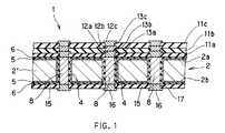
図1は、本発明の多層配線基板の一実施形態を示す部分縦断面図である。図1において、本発明の多層配線基板1は、コア基板2と、このコア基板2の表面2a上に電気絶縁層を介して形成された配線と、裏面2b上に電気絶縁層を介して形成された配線と、を備えている。
多層配線基板1を構成するコア基板2は、コア材2′に複数のスルーホール4が形成されたものであり、各スルーホール4には導電性物質8が充填され、この導電性物質8によりスルーホール4を介した表面2aと裏面2bの導通がなされている。Hereinafter, embodiments of the present invention will be described with reference to the drawings.
[Multilayer wiring board]
FIG. 1 is a partial longitudinal sectional view showing an embodiment of a multilayer wiring board according to the present invention. In FIG. 1, a multilayer wiring board 1 of the present invention is formed with a
A
コア基板2に形成されたスルーホール4の開口径は、10〜100μm、好ましくは10〜70μmの範囲内である。スルーホールの開口径が上記の範囲未満であると、スルーホール形成加工が困難となり、また、上記の範囲を超えると、スルーホールの密度を高くしたり、スルーホールの形成数を多くすることに限度があり好ましくない。スルーホール4の内壁面、およびコア基板の両面2a,2bには、導電性物質拡散防止層5と絶縁膜6が設けられており、絶縁膜6は、導電性物質拡散防止層5と導電性物質8との間に介在している。 The opening diameter of the through
コア基板2の表面2a上に形成された配線は、図示例では多層配線であり、コア基板2の表面2a上に電気絶縁層11aを介しビア13aにてスルーホール4内の導電性物質8に接続されるように形成された1層目の配線12aと、この1層目の配線12a上に2層目の電気絶縁層11bを介しビア13bにて所定の1層目配線12aに接続されるように形成された2層目の配線12bと、この2層目の配線12b上に3層目の電気絶縁層11cを介しビア13cにて所定の2層目配線12bに接続されるように形成された3層目の配線12cとからなる。 The wiring formed on the
また、コア基板2の裏面2b上に形成された配線は、図示例では単層配線であり、コア基板2の裏面2b上に電気絶縁層15を介しビア17にてスルーホール4内の導電性物質8に接続されるように形成された配線16である。
尚、各配線12a,12b,12c,16および各ビア13a,13b,13cは、例えば、銅、銀等の薄膜である下地金属層を介して、導電性物質8上、下層の電気絶縁層上、ビア上に形成されていてもよい。In addition, the wiring formed on the
The
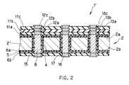
図2は、本発明の多層配線基板の他の実施形態を示す部分縦断面図である。図2において、本発明の多層配線基板1′は、コア基板2に設けられている導電性物質拡散防止層5と絶縁膜6の積層構造が上述の多層配線基板1と相違する他は、上述の多層配線基板1と同じものであり、共通の部材には同じ部材番号を付している。
この多層配線基板1′では、スルーホール4の内壁面、およびコア基板の両面2a,2bに、第1の絶縁膜6a、導電性物質拡散防止層5、第2の絶縁膜6bが、この順に積層されて配設されている。したがって、スルーホール4内においては、導電性物質拡散防止層5と導電性物質8との間に第2の絶縁膜6bが介在している。
尚、第1の絶縁膜6aと第2の絶縁膜6bは、構成材料が同じものであってもよい。FIG. 2 is a partial longitudinal sectional view showing another embodiment of the multilayer wiring board of the present invention. 2, the multilayer wiring board 1 ′ of the present invention is the same as that described above except that the laminated structure of the conductive material
In this multilayer wiring board 1 ′, the first insulating
The first
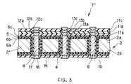
また、図3は、本発明の多層配線基板の他の実施形態を示す部分縦断面図である。図3において、本発明の多層配線基板1″は、コア基板2に設けられている導電性物質拡散防止層5と絶縁膜6の積層構造が上述の多層配線基板1と相違する他は、上述の多層配線基板1と同じものであり、共通の部材には同じ部材番号を付している。 FIG. 3 is a partial longitudinal sectional view showing another embodiment of the multilayer wiring board of the present invention. 3, the multilayer wiring board 1 ″ of the present invention is the same as that described above except that the laminated structure of the conductive material
この多層配線基板1″では、スルーホール4の内壁面、およびコア基板の両面2a,2bに、第1の絶縁膜6a、第2の絶縁膜6b、導電性物質拡散防止層5、第3の絶縁膜6cが、この順に積層されて配設されている。したがって、スルーホール4内においては、導電性物質拡散防止層5と導電性物質8との間に第3の絶縁膜6cが介在している。
尚、第2の絶縁膜6bと第3の絶縁膜6cは、構成材料が同じものであってもよく、また、第1の絶縁膜6a、第2の絶縁膜6bおよび第3の絶縁膜6cのすべてが、構成材料が同じものであってもよい。In this multilayer wiring board 1 ″, the first insulating
Note that the second
図4は、本発明の多層配線基板の他の実施形態を示す部分縦断面図である。図4において、本発明の多層配線基板21は、コア基板22と、このコア基板22の表面22a上に電気絶縁層を介して形成された配線と、裏面22b上に電気絶縁層を介して形成された配線と、を備えている。
多層配線基板21を構成するコア基板22は、コア材22′に複数のスルーホール24が形成されたものであり、各スルーホール4には導電性物質28が充填され、この導電性物質28によりスルーホール24を介した表面22aと裏面22bの導通がなされている。FIG. 4 is a partial longitudinal sectional view showing another embodiment of the multilayer wiring board of the present invention. In FIG. 4, the
The
コア基板22に形成されたスルーホール4の開口径は、10〜100μm、好ましくは10〜70μmの範囲内である。スルーホールの開口径が上記の範囲未満であると、スルーホール形成加工が困難となり、また、上記の範囲を超えると、スルーホールの密度を高くしたり、スルーホールの形成数を多くすることに限度があり好ましくない。スルーホール24の内壁面、およびコア基板の表面22aには、導電性物質拡散防止層25と絶縁膜26が設けられており、絶縁膜26が導電性物質拡散防止層25と導電性物質28との間に介在している。また、コア基板22の裏面22bには、絶縁膜23が設けられている。 The opening diameter of the through
コア基板22の表面22a上に形成された配線は、図示例では多層配線であり、コア基板22の表面22a上に電気絶縁層31aを介しビア33aにてスルーホール24内の導電性物質28に接続されるように形成された1層目の配線32aと、この1層目の配線32a上に2層目の電気絶縁層31bを介しビア33bにて所定の1層目配線32aに接続されるように形成された2層目の配線32bと、この2層目の配線32b上に3層目の電気絶縁層31cを介しビア33cにて所定の2層目配線32bに接続されるように形成された3層目の配線32cとからなる。 The wiring formed on the
また、コア基板22の裏面22b上に形成された配線は、図示例では単層配線であり、コア基板22の裏面22b上に電気絶縁層35を介しビア37にてスルーホール24内の導電性物質28に接続されるように形成された配線36である。
尚、各配線32a,32b,32c,36および各ビア33a,33b,33cは、例えば、銅、銀等の薄膜である下地金属層を介して、導電性物質28上、下層の電気絶縁層上、ビア上に形成されていてもよい。In addition, the wiring formed on the
The
このような多層配線基板21においても、導電性物質拡散防止層25と絶縁膜26の積層構造を、上述の多層配線基板1′,1″のように、第1の絶縁膜と第2の絶縁膜とで導電性物質拡散防止層25を挟むような積層構造、あるいは、第1、第2の絶縁膜と第3の絶縁膜とで導電性物質拡散防止層25を挟むような積層構造としてもよい。 Also in such a
上述のような本発明の多層配線基板1,1′,1″,21では、スルーホール4,24内部に導電性物質8,28が充填され、この導電性物質8,28に接続するビア13a,17,33a,37を介して1層目の配線12a,16,32a,36が形成された構造、すなわち、スルーホール4,24直上にビア13a,17,33a,37を備える構造であるため、多層配線の配線設計の自由度を高くすることができる。また、スルーホール4,24内には樹脂が充填されていないので、スルーホール4,24直上に配置されたビア13a,17,33a,37へのコア基板2の熱収縮や熱膨張による応力集中が発生し難く、接続信頼性が高いものとなる。さらに、スルーホール4,24の狭ピッチ化が可能であるとともに、スルーホール4,24間のスペースの確保が容易であり、このスペースに必要な配線を形成することができるので、所望の高密度配線をより少ない層数で形成することができ、薄型の半導体装置の製造が可能となる。また、スルーホール4,24の内壁面に設けられた導電性物質拡散防止層5,25によって、スルーホール内部に充填された導電性物質8,28の構成物質がコア基板2,22中に拡散することが阻止される。さらに、導電性物質8,28と導電性物質拡散防止層5,25との間に位置する絶縁膜6,26(第2の絶縁膜6b,第3の絶縁膜6c)により、導電性物質8,28が拡散することによる導電性物質拡散防止層5,25の導電性変化が防止される。これにより、導電性物質拡散防止層5,25が設計通りの電気特性を発現することができ、導電性物質拡散防止効果がより高いものとなり、スルーホール4,24の狭ピッチ化を進めても隣接するスルーホール4,24間の短絡を防止することができる。 In the multilayer wiring board 1, 1 ′, 1 ″, 21 according to the present invention as described above, the
本発明の多層配線基板1を構成するコア基板2,22は、例えば、シリコン、ガラス等のコア材2′,22′を用いて作製することができる。コア基板2,22の厚みは、50〜725μm、好ましくは300〜625μmの範囲内である。コア基板2,22の厚みが50μm未満であると、支持体として充分な強度を保持できず、725μmを超えると、半導体装置の薄型化に支障を来たすことになり好ましくない。
スルーホール4,24の内壁面に形成される導電性物質拡散防止層5,25は、緻密であり、コア基板2,22中への導電性物質の拡散を防止し得る薄膜であれば特に制限はなく、例えば、窒化チタン、チタン、クロム等の薄膜層とすることができる。この導電性物質拡散防止層5の厚みは、例えば、10〜50nmの範囲で設定することができる。The
The conductive material
多層配線基板1を構成する絶縁膜6、多層配線基板1′を構成する第2の絶縁膜6b、多層配線基板1″を構成する第2の絶縁膜6bと第3の絶縁膜6c、多層配線基板21を構成する絶縁膜26は、二酸化珪素、窒化珪素等の無機化合物からなる薄膜とすることができ、厚みは10〜4000nm、好ましくは50〜1000nm程度とすることができる。
また、多層配線基板1′を構成する第1の絶縁膜6a、多層配線基板1″を構成する第1の絶縁膜6a、および、多層配線基板21を構成する絶縁膜23は、上述のような絶縁膜であってよく、また、コア基板2がシリコンコア基板である場合には、熱酸化により形成した酸化珪素膜であってもよい。Insulating
Further, the first insulating
コア基板2,22の各スルーホール4,24に充填された導電性物質8,28としては、例えば、フィルド電解めっきによりスルーホール内に形成された銅等の導電性金属とすることができる。また、銅粒子、銀粒子等の導電性粒子を含有した導電性ペーストを用いることができる。但し、導電性ペーストを導電性物質8,28として用いる場合、コア基板2,22の熱収縮や熱膨張によるビア13a,17,33a,37への応力集中を抑制するために、導電性粒子の含有率が80体積%以上であることが好ましい。 The
コア基板2,22の表面2a,22a上の1層目の配線12a,32a、2層目の配線12b,32b、3層目の配線12c,32cの材質、ビア13a,13b,13c,33a,33b,33cの材質、および、裏面2b,22b上の配線16,36の材質、ビア17,37の材質は、例えば、銅、ニッケル等の導電性材料とすることができる。このような各層の配線の厚みは、例えば、3〜20μmの範囲で設定することができ、ビアの径は、例えば、20〜100μmの範囲で設定することができる。 The
また、電気絶縁層11a,11b,11c,31a,31b,31cおよび電気絶縁層15,35の材質は、エポキシ樹脂、ベンゾシクロブテン樹脂、カルド樹脂、ポリイミド樹脂,フルオレン等の有機絶縁性材料とすることができる。このような電気絶縁層の厚みは、例えば、3〜20μmの範囲で設定することができる。
尚、上述の実施形態では、コア基板2,22の表面2a,22aに配線12a,12b,12c,32a,32b,32cが形成され、裏面に配線16,36が形成されているが、本発明ではコア基板に形成する配線層の積層数には制限はない。
また、本発明の多層配線基板は、最表面層の配線を、半導体チップ搭載用の端子パッドを有するものとすることができる。さらに、このような端子パッドの表面に半田層を備えるものであってもよい。The materials of the electrical insulating
In the above-described embodiment, the
In the multilayer wiring board of the present invention, the wiring on the outermost surface layer may have a terminal pad for mounting a semiconductor chip. Furthermore, a solder layer may be provided on the surface of such a terminal pad.
多層配線基板の製造方法
次に、本発明の多層配線基板の製造方法を図面を参照しながら説明する。
図5乃至図7は、図1に示される多層配線基板1を例として、本発明の多層配線基板の製造方法の一実施形態を示す工程図である。
本発明の多層配線基板の製造方法では、コア基板用のコア材2′の一方の面2′aに所定の開口9aを有するマスクパターン9を形成し、このマスクパターン9をマスクとしてプラズマを利用したドライエッチング法であるICP−RIE(Inductive Coupled Plasma - Reactive Ion Etching)によりコア材2′に所定の深さで微細孔4′を穿設する(図5(A))。Next, amethod for manufacturing a multilayer wiring board according to the present invention will be described with reference to the drawings.
FIGS. 5 to 7 are process diagrams showing an embodiment of the method for manufacturing a multilayer wiring board according to the present invention, taking the multilayer wiring board 1 shown in FIG. 1 as an example.
In the method for manufacturing a multilayer wiring board according to the present invention, a
コア材2′は、例えば、シリコン、ガラス等を使用することができる。また、マスクパターン9は、ドライエッチング耐性のある材料を用いて形成することができ、例えば、ノボラック樹脂を用いたポジ型レジストを使用して形成することができる。また、コア材2′に比べエッチング選択比が小さい(エッチング速度が小さい)材料、例えば、シリコンからなるコア材2′に対して、酸化シリコン、窒化シリコン等を使用してマスクパターン21を形成することができる。
形成する微細孔4′の開口径は、10〜100μm、好ましくは10〜70μmの範囲内で適宜設定することができる。また、微細孔4′の深さは、作製するコア基板の厚み(例えば、50〜725μm)を考慮して設定することができ、例えば、70〜745μmの範囲内で適宜設定することができる。本発明の製造方法では、スルーホール用の微細孔4′をプラズマを利用したドライエッチング法により形成するので、開口径の小さいスルーホールの形成が可能となる。For example, silicon or glass can be used for the
The opening diameter of the
次に、コア材2′からマスクパターン9を除去し、コア材2′の他方の面2′bを研磨して、微細孔4′を露出させてスルーホール4を形成し、その後、コア材2′の両面およびスルーホール4の内壁面に導電性物質拡散防止層5と絶縁膜6を成膜する(図5(B))。
導電性物質拡散防止層5は、窒化チタン、チタン、クロム等からなる薄膜とすることができる。このような導電性物質拡散防止層5は、例えば、MO−CVD(Metal Organic - Chemical Vapor Deposition)やスパッタリング法により形成することができ、特にスルーホール4の開口径が70μm以下の場合には、MO−CVDにより形成することが好ましい。Next, the
The conductive substance
また、絶縁膜6は、例えば、プラズマCVD(Plasma Enhanced - Chemical Vapor Deposition)で形成した酸化シリコン膜、窒化シリコン膜等とすることができ、このような絶縁膜6の厚みは、例えば、500〜1000nmの範囲で設定することができる。
尚、導電性物質拡散防止層5と絶縁膜6の積層構造を、上述の多層配線基板1′(図2)のように、第1の絶縁膜6a、導電性物質拡散防止層5、第2の絶縁膜6bがこの順に積層された構造、多層配線基板1″(図3)のように、第1の絶縁膜6a、第2の絶縁膜6b、導電性物質拡散防止層5、第3の絶縁膜6cがこの順に積層された構造とする場合には、第1の絶縁膜6a、第2の絶縁膜6b、第3の絶縁膜6cは、上述の絶縁膜6と同様にして形成することができる。また、第1の絶縁膜6aは、コア材2′がシリコンである場合には、熱酸化を施して酸化珪素膜として形成してもよい。Further, the insulating
Note that the laminated structure of the conductive material
次に、絶縁膜6上に下地導電層7を形成する(図5(C))。この下地導電層7は、例えば、銅、ニッケル等の薄膜、チタン/銅の積層薄膜等とすることができる。下地導電層7の形成は、例えば、MO−CVD(Metal Organic - Chemical Vapor Deposition)やスパッタリング法により行うことができ、特にスルーホール4の開口径が70μm以下の場合には、MO−CVDにより形成することが好ましい。このような下地導電層7は、スルーホール4の内壁面に存在する絶縁膜6を被覆する必要はあるが、コア基板2の両面には、所望の部位に形成するものであってもよい。
次いで、下地導電層7、絶縁膜6上に所望レジスト膜10a,10bを形成し、下地導電層7を給電層として、フィルド電解めっきによりスルーホール4内に銅、ニッケル等の導電性物質8を充填する(図5(D))。レジスト膜10a,10bは、公知の感光性レジスト材料を使用して形成することができ、その厚みは、例えば、1〜100μmの範囲で設定することができる。Next, a base
Next, desired resist
このフィルド電解めっきでは、レジスト膜10a,10bが導電性物質拡散防止層5と密着するのではなく、絶縁膜6や下地導電層7と密着しているので、その密着強度が高く、導電性物質8が絶縁膜6や下地導電層7とレジスト膜10a,10bとの界面に侵入して不要な広がりを生じることがない。このため、レジスト膜10a,10bのパターンを反映した高い精度で導電性物質8を充填することができる。
尚、スルーホール4内に、導電性物質8として導電性ペーストをスクリーン印刷等の方法により充填してもよい。使用する導電性ペーストは、銅粒子、銀粒子等の導電性粒子を80体積%以上含有した導電性ペーストであることが望ましい。In this filled electrolytic plating, the resist
The through
次に、レジスト膜10a,10bを除去し、必要に応じてコア材2′上に突出する余分な導電性物質8を研磨して除去することにより、スルーホール4内のみに導電性物質8を残す。これにより、スルーホール4内に充填された導電性物質8による表裏の導通がとられたコア基板2が得られる(図6(A))。上記のような余分な導電性物質8を研磨除去する場合にも、上述のように、導電性物質8が絶縁膜6や下地導電層7とレジスト膜10a,10bとの界面に侵入して不要な広がりを生じることがないので、絶縁膜6や導電性物質拡散防止層5を損傷することなく、余分な導電性物質8のみを研磨除去することができる。 Next, the resist
次に、コア基板2の両面に1層目の配線の電気絶縁層として、感光性絶縁材料を塗布し、所定のパターンで露光して現像することにより、電気絶縁層11a,15を形成する(図6(B))。電気絶縁層11a,15は、例えば、ベンゾシクロブテン、ポリイミド、フルオレン等の感光性絶縁材料を使用して形成することができ、その厚みは、例えば、3〜20μmの範囲で設定することができる。 Next, a photosensitive insulating material is applied to both surfaces of the
次いで、この電気絶縁層11a,15を覆うように、下地金属層12′a,16′を形成し、電気絶縁層11a,15上にレジストパターン19を形成する(図6(C))。下地金属層12′a,16′は、スパッタリング法等により形成した薄膜であってよく、例えば、銅、銀等の薄膜であってよい。また、下地金属層12′a,16′の構造を、上記のような薄膜と、クロム、チタン、窒化チタン等の密着膜との積層構造としてもよい。このような下地金属層の厚みは、例えば、50〜350nmの範囲で設定することができる。
また、レジストパターン19は、スルーホール4内に充填された導電性物質8上の下地金属層12′a,16′が露出するような開口19aを有している。Next, base metal layers 12'a and 16 'are formed so as to cover the electrical insulating
The resist
次いで、このジストパターン19をマスクとし、下地金属層12′a,16′を給電層として電解めっきを行い、その後、レジストパターン19を除去する。これにより、スルーホール4内に充填された導電性物質8にビア13aを介して接続された配線12aと、ビア17を介して接続された配線16とを形成する(図7(A))。このような配線、ビアの材質は、例えば、銅、ニッケル等の導電性材料を使用することができる。
その後、電気絶縁層11a,15上に存在している余分な下地金属層12′a,16′を除去する。これにより、コア基板2の両面に電気絶縁層を介した1層目の配線が形成され、この配線は、スルーホール4内に充填された導電性物質8にビアを介して接続されたものとなる(図7(B))。
その後、図6(B)〜図7(B)の工程を繰り返すことにより、コア基板2の表面2a側および/または裏面2b側に、更に任意の層数の配線を形成して、所望の多層配線基板を得ることができる。Next, electrolytic plating is performed using the resist
Thereafter, excess base metal layers 12'a and 16 'existing on the electrical insulating
Thereafter, by repeating the steps of FIG. 6B to FIG. 7B, an arbitrary number of wirings are further formed on the
図8乃至図9は、図2に示される多層配線基板1′を例として、本発明の多層配線基板の製造方法の他の実施形態を示す工程図である。
本発明の多層配線基板の製造方法では、まず、上述の実施態様と同様にして、コア材2′にスルーホール4を形成する。その後、コア材2′の両面およびスルーホール4の内壁面に第1の絶縁膜6aを成膜する(図8(A))。第1の絶縁膜6aは、例えば、プラズマCVDで形成した酸化シリコン膜、窒化シリコン膜等とすることができ、このような絶縁膜6aの厚みは、例えば、500〜1000nmの範囲で設定することができる。また、第1の絶縁膜6aは、コア材2′がシリコンである場合には、熱酸化を施すことにより酸化珪素膜として形成してもよい。8 to 9 are process diagrams showing another embodiment of the method for manufacturing a multilayer wiring board according to the present invention, taking the multilayer wiring board 1 'shown in FIG. 2 as an example.
In the method for manufacturing a multilayer wiring board according to the present invention, first, the through
次に、第1の絶縁膜6a上に導電性物質拡散防止層5と第2の絶縁膜6bを成膜する(図8(B))。導電性物質拡散防止層5と第2の絶縁膜6bの形成は、上述の導電性物質拡散防止層5と絶縁膜6の形成と同様に行うことができる。
尚、上述の多層配線基板1(図1)のように、導電性物質拡散防止層5、絶縁膜6がこの順に積層された構造、多層配線基板1″(図3)のように、第1の絶縁膜6a、第2の絶縁膜6b、導電性物質拡散防止層5、第3の絶縁膜6cがこの順に積層された構造とすることもできる。Next, the conductive material
As in the multilayer wiring board 1 (FIG. 1) described above, a structure in which the conductive material
次に、コア材2′の一方の面(図示例では面2′b側)の第2の絶縁膜6b上に下地導電層7を形成する(図8(C))。この下地導電層7は、例えば、銅、ニッケル等の薄膜、チタン/銅の積層薄膜等とすることができる。下地導電層7の形成は、例えば、蒸着法、スパッタリング法、MO−CVD等により行うことができる。
次いで、下地導電層7上と、コア材2′の他方の面(図示例では面2′a側)の第2の絶縁膜6b上に所望レジスト膜10a、10bを形成し、下地導電層7を給電層として、フィルド電解めっきにより、スルーホール4内に一方向(矢印a方向)から銅、ニッケル等の導電性物質8を析出、成長させて充填する(図8(D))。レジスト膜10a,10bは、公知の感光性レジスト材料を使用して形成することができ、その厚みは、例えば、1〜100μmの範囲で設定することができる。Next, the base
Next, desired resist
このフィルド電解めっきでは、レジスト膜10a,10bが導電性物質拡散防止層5と密着するのではなく、第2の絶縁膜6bや下地導電層7と密着しているので、その密着強度が高く、導電性物質8が第2の絶縁膜6bや下地導電層7とレジスト膜10a,10bとの界面、特に、導電性物質8の析出、成長方向に位置する第2の絶縁膜6bとレジスト膜10aとの界面に侵入することが阻止され、不要な広がりを生じることがない。このため、レジスト膜10a,10bのパターンを反映した高い精度で導電性物質8を充填することができる。 In this filled electrolytic plating, the resist
次に、レジスト膜10a,10bを除去し、必要に応じてコア材2′上に突出する余分な導電性物質8を研磨して除去することにより、スルーホール4内のみに導電性物質8を残す。これにより、スルーホール4内に充填された導電性物質8による表裏の導通がとられたコア基板2が得られる(図9(A))。上記のような余分な導電性物質8を研磨除去する場合にも、上述のように、導電性物質8が第2の絶縁膜6bや下地導電層7とレジスト膜10a,10bとの界面に侵入して不要な広がりを生じることがないので、第2の絶縁膜6bや導電性物質拡散防止層5を損傷することなく、余分な導電性物質8のみを研磨除去することができる。
次に、コア基板2の両面に1層目の配線の電気絶縁層として、感光性絶縁材料を塗布し、所定のパターンで露光して現像することにより、電気絶縁層11a,15を形成し、この電気絶縁層11a,15を覆うように、下地金属層12′a,16′を形成する(図9(B))。下地金属層12′a,16′の形成は、上述の実施形態と同様とすることができる。Next, the resist
Next, a photosensitive insulating material is applied to both surfaces of the
次いで、電気絶縁層11a,15上にレジストパターンを形成し、このジストパターンをマスクとし、下地金属層12′a,16′を給電層として電解めっきを行う。その後、レジストパターンを除去し、電気絶縁層11a,15上に露出している余分な下地金属層12′a,16′を除去する。これにより、スルーホール4内に充填された導電性物質8にビア13aを介して接続された配線12aと、ビア17を介して接続された配線16とを形成する(図9(C))。尚、上記のレジストパターンは、スルーホール4内に充填された導電性物質8上の下地金属層12′a,16′が露出するような開口を有するものであり、上述の実施形態と同様にして形成することができる。
その後、図9(B)〜図9(C)の工程を繰り返すことにより、コア基板2の表面2a側および/または裏面2b側に、更に任意の層数の配線を形成して、所望の多層配線基板を得ることができる。Next, a resist pattern is formed on the electrical insulating
Thereafter, by repeating the steps of FIG. 9B to FIG. 9C, an arbitrary number of wirings are further formed on the
図10乃至図11は、図4に示される多層配線基板21を例として、本発明の多層配線基板の製造方法の他の実施形態を示す工程図である。
本発明の多層配線基板の製造方法では、コア基板用のコア材22′の一方の面22′aに所定の開口29aを有するマスクパターン29を形成し、このマスクパターン29をマスクとしてプラズマを利用したドライエッチング法であるICP−RIE(Inductive Coupled Plasma - Reactive Ion Etching)によりコア材22′に所定の深さで微細孔24′を穿設する(図10(A))。
コア材22′は上述の実施形態のコア材2′と同様のものを使用することができ、また、マスクパターン29は、上述の実施形態のマスクパターン9と同様に形成することができる。10 to 11 are process diagrams showing another embodiment of the method for manufacturing a multilayer wiring board according to the present invention, taking the
In the method for manufacturing a multilayer wiring board according to the present invention, a
The core material 22 'can be the same as the
また、形成する微細孔24′の開口径は、10〜100μm、好ましくは10〜70μmの範囲内で適宜設定することができる。また、微細孔4′の深さは、作製するコア基板の厚み(例えば、50〜725μm)を考慮して設定することができ、例えば、70〜745μmの範囲内で適宜設定することができる。本発明の製造方法では、スルーホール用の微細孔4′をプラズマを利用したドライエッチング法により形成するので、開口径の小さいスルーホールの形成が可能となる。 Further, the opening diameter of the
次に、コア材22′からマスクパターン29を除去し、コア材22′の表面および微細孔24′の内壁面に導電性物質拡散防止層25と、この導電性物質拡散防止層25を被覆する絶縁膜26を成膜する(図10(B))。導電性物質拡散防止層25と絶縁膜26の形成は、上述の実施形態における導電性物質拡散防止層5と絶縁膜6の形成と同様に行うことができる。尚、上述の多層配線基板1′(図2)と同様に、第1の絶縁膜、導電性物質拡散防止層、第2の絶縁膜がこの順に積層された構造、あるいは、多層配線基板1″(図3)と同様に、第1の絶縁膜、第2の絶縁膜、導電性物質拡散防止層、第3の絶縁膜がこの順に積層された構造とすることもできる。 Next, the
次に、絶縁膜26上に所望の下地導電層27を形成し、この下地導電層27、絶縁膜26上に所望レジスト膜30を形成する。下地導電層27は、微細孔24′の内壁面に存在する絶縁膜26を被覆する必要はあるが、コア材22上には、所望の部位に形成するものであってもよい。そして、下地導電層27を給電層として、フィルド電解めっきにより微細孔24′内に銅、ニッケル等の導電性物質28を充填する(図10(C))。下地導電層27、レジスト膜30の形成は、上述の実施形態の下地導電層7、レジスト膜30の形成と同様に行うことができる。 Next, a desired base
このフィルド電解めっきでは、レジスト膜30が導電性物質拡散防止層25と密着するのではなく、絶縁膜26や下地導電層27と密着しているので、その密着強度が高く、導電性物質28が絶縁膜26や下地導電層27とレジスト膜30との界面に侵入して不要な広がりを生じることがない。このため、レジスト膜30のパターンを反映した高い精度で導電性物質28を充填することができる。 In this filled electrolytic plating, the resist
次に、コア材22′上に突出する余分な導電性物質28を研磨して除去し、微細孔24′内のみに導電性物質28を残す。また、コア材22′の他方の面22′bを研磨して、微細孔24′を露出させてスルーホール24を形成し、この研磨面に絶縁膜23を形成する。これにより、スルーホール24内に充填された導電性物質28による表裏の導通がとられたコア基板22が得られる(図11(A))。上記のような余分な導電性物質28を研磨除去する場合にも、上述のように、導電性物質28が絶縁膜26や下地導電層27とレジスト膜30との界面に侵入して不要な広がりを生じることがないので、絶縁膜26や導電性物質拡散防止層25を損傷することなく、余分な導電性物質28のみを研磨除去することができる。 Next, excess
絶縁膜23の形成は、例えば、プラズマCVD(Chemical Vapor Deposition)で形成した酸化シリコン膜、窒化シリコン膜等とすることができ、このような絶縁膜23の厚みは、例えば、500〜1000nmの範囲で設定することができる。また、コア材22′がシリコンである場合には、熱酸化を施すことにより酸化珪素膜からなる絶縁膜23を形成してもよい。
次に、コア基板22の両面に1層目の配線の電気絶縁層として、感光性絶縁材料を塗布し、所定のパターンで露光して現像することにより、電気絶縁層31a,35を形成し、この電気絶縁層31a,35を覆うように、下地金属層32′a,36′を形成する(図11(B))。下地金属層32′a,36′の形成は、上述の実施形態における下地金属層12′a,16′の形成と同様とすることができる。The insulating
Next, a photosensitive insulating material is applied to both surfaces of the
次いで、電気絶縁層31a,35上にレジストパターンを形成し、このジストパターンをマスクとし、下地金属層32′a,36′を給電層として電解めっきを行う。その後、レジストパターンを除去し、電気絶縁層31a,35上に露出している余分な下地金属層32′a,36′を除去する。これにより、スルーホール24内に充填された導電性物質28にビア33aを介して接続された配線32aと、ビア37を介して接続された配線36とを形成する(図11(C))。尚、上記のレジストパターンは、スルーホール24内に充填された導電性物質28上の下地金属層32′a,36′が露出するような開口を有するものであり、上述の実施形態と同様にして形成することができる。 Next, a resist pattern is formed on the electrical insulating
その後、図11(B)〜図11(C)の工程を繰り返すことにより、コア基板22の表面22a側および/または裏面22b側に、更に任意の層数の配線を形成して、所望の多層配線基板を得ることができる。
尚、上述の多層配線基板と製造方法の実施形態は一例であり、本発明は、これらの実施形態に限定されるものではない。After that, by repeating the steps of FIG. 11B to FIG. 11C, an arbitrary number of layers of wiring are formed on the
The above-described embodiments of the multilayer wiring board and the manufacturing method are examples, and the present invention is not limited to these embodiments.
次に、具体的実施例を挙げて本発明を更に詳細に説明する。
[実施例1]
コア材として、厚み625μm、直径150mmのシリコン基板を準備し、このコア材の一方の面にノボラック系のポジ型レジスト材料(東京応化工業(株)製PMER−P−LA900PM)を塗布し、スルーホール形成用のフォトマスクを介して露光、現像した。これにより、開口径が10μm、30μm、70μm、100μmの4種の円形開口を有し、開口径10μmの開口が20μmピッチ、開口径30μmの開口が60μmピッチ、開口径70μmの開口が150μmピッチ、開口径100μmの開口が200μmピッチで、それぞれ形成されたマスクパターンを形成した。Next, the present invention will be described in more detail with specific examples.
[Example 1]
A silicon substrate having a thickness of 625 μm and a diameter of 150 mm is prepared as a core material, and a novolac-based positive resist material (PMER-P-LA900PM manufactured by Tokyo Ohka Kogyo Co., Ltd.) is applied to one side of the core material. It exposed and developed through the photomask for hole formation. Accordingly, there are four types of circular openings with an opening diameter of 10 μm, 30 μm, 70 μm, and 100 μm, openings with an opening diameter of 10 μm are 20 μm pitch, openings with an opening diameter of 30 μm are 60 μm pitch, and openings with an opening diameter of 70 μm are 150 μm pitch, A mask pattern was formed in which openings with an opening diameter of 100 μm were formed at a pitch of 200 μm.
次に、このマスクパターンをマスクとして、コア材にICP−RIE(Inductive Coupled Plasma - Reactive Ion Etching)によりドライエッチングを行い複数の微細孔を形成した。この微細孔の深さは約350μmとした。
次に、不要なマスクパターンを除去し後、コア材の裏面を研磨して、微細孔を露出させてスルーホールを形成した。次いで、洗浄後、MO−CVD(Metal Organic - Chemical Vapor Deposition)により、窒化チタンからなる厚み10nmの導電性物質拡散防止層をコア材の両面とスルーホール内壁面に形成した。Next, using this mask pattern as a mask, the core material was dry-etched by ICP-RIE (Inductive Coupled Plasma-Reactive Ion Etching) to form a plurality of fine holes. The depth of the fine holes was about 350 μm.
Next, after removing an unnecessary mask pattern, the back surface of the core material was polished to expose fine holes to form through holes. Next, after cleaning, a conductive material diffusion prevention layer made of titanium nitride and having a thickness of 10 nm was formed on both surfaces of the core material and the inner wall surface of the through hole by MO-CVD (Metal Organic-Chemical Vapor Deposition).
次に、この導電性物質拡散防止層を被覆するように、プラズマCVD(Plasma Enhanced - Chemical Vapor Deposition)により、二酸化珪素からなる厚み3μmの絶縁膜を形成した。
次いで、スクリーン印刷により導電性ペースト(平均粒径2.5μmの銀コート銅粒子を85体積%含有)をスルーホール内に充填し、硬化処理(160℃、20分間)を施した。その後、コア材の表面上に盛り上がっている導電性ペーストを研磨により除去し、スルーホール内の導電性ペーストとコア材面が同一面となるようにした。これにより、開口径が10μm、30μm、70μm、100μmの4種のスルーホールを有し、各スルーホール内に充填された導電性ペーストからなる導電性物質による表裏の導通がとられたコア基板(図1に示されるようなコア基板)が得られた。Next, an insulating film made of silicon dioxide and having a thickness of 3 μm was formed by plasma CVD (plasma enhanced chemical vapor deposition) so as to cover the conductive substance diffusion prevention layer.
Next, a conductive paste (containing 85 volume% of silver-coated copper particles having an average particle diameter of 2.5 μm) was filled in the through holes by screen printing, and subjected to curing treatment (160 ° C., 20 minutes). After that, the conductive paste raised on the surface of the core material was removed by polishing so that the conductive paste in the through hole and the core material surface were the same surface. As a result, the core substrate (which has four through-holes with an opening diameter of 10 μm, 30 μm, 70 μm, and 100 μm) and is electrically connected to each other by a conductive substance made of a conductive paste filled in each through-hole ( A core substrate as shown in FIG. 1 was obtained.
次に、コア基板の両面に、感光性ベンゾシクロブテン(DOW社製Cyclotene-4024-40)を塗布し、所定のパターンで露光して現像し、硬化させることにより、1層目の配線の電気絶縁層(厚み10μm)を形成した。この電気絶縁層は、スルーホール内に充填された導電性ペーストが露出するパターンであった。
次いで、電気絶縁層を覆うように、スパッタリング法によりクロム薄膜(厚み30nm)と銅薄膜(厚み200nm)の積層構造である下地金属層を形成した。Next, photosensitive benzocyclobutene (Cyclotene-4024-40, manufactured by DOW) is applied to both surfaces of the core substrate, exposed in a predetermined pattern, developed, and cured, whereby the electrical wiring of the first layer is An insulating layer (
Next, a base metal layer having a laminated structure of a chromium thin film (
次に、スルーホール内に充填された導電性ペースト上の下地金属層が露出するように、電気絶縁層上にレジストパターンを形成した。その後、このレジストパターンをマスクとし、下地金属層を給電層として電解めっきを行い、厚み4μmの銅層を形成した。次いで、レジストパターンを除去し、電気絶縁層上に露出している余分な下地金属層を除去した。この下地金属層の除去は、まず、過硫酸ナトリウム溶液にて銅薄膜を除去し、次いで、アルカリ性過マンガン酸ナトリウム溶液でクロム薄膜を除去した。これにより、スルーホール内に充填された導電性物質にビアを介して接続された配線を、コア基板の両面に形成した。
上記の配線形成を繰り返すことにより、2層以上の配線を形成して、所望の多層配線基板を得ることができた。Next, a resist pattern was formed on the electrical insulating layer so that the base metal layer on the conductive paste filled in the through hole was exposed. Thereafter, electrolytic plating was performed using the resist pattern as a mask and the base metal layer as a power feeding layer to form a copper layer having a thickness of 4 μm. Next, the resist pattern was removed, and the excess base metal layer exposed on the electrical insulating layer was removed. The removal of the base metal layer was performed by first removing the copper thin film with a sodium persulfate solution and then removing the chromium thin film with an alkaline sodium permanganate solution. As a result, wirings connected to the conductive material filled in the through holes via vias were formed on both surfaces of the core substrate.
By repeating the above wiring formation, two or more layers of wiring were formed, and a desired multilayer wiring board could be obtained.
[実施例2]
まず、実施例1と同様にコア材を用いて、ICP−RIEによりドライエッチングを行い複数の微細孔を形成した。この微細孔の深さは約350μmとした。
次に、微細孔を設けたコア材面および微細孔の内壁面に、MO−CVDにより、窒化チタンからなる厚み10nmの導電性物質拡散防止層を形成した。次いで、この導電性物質拡散防止層を被覆するように、プラズマCVDにより、二酸化珪素からなる厚み3μmの絶縁膜を形成した。[Example 2]
First, using the core material as in Example 1, dry etching was performed by ICP-RIE to form a plurality of fine holes. The depth of the fine holes was about 350 μm.
Next, a conductive material diffusion prevention layer made of titanium nitride and having a thickness of 10 nm was formed by MO-CVD on the core material surface provided with the micropores and the inner wall surface of the micropores. Subsequently, an insulating film made of silicon dioxide and having a thickness of 3 μm was formed by plasma CVD so as to cover the conductive substance diffusion prevention layer.
次に、絶縁膜上に銅からなる厚み200nmの下地導電層をスパッタリング法により形成し、その後、感光性フィルムレジスト(旭化成エレクトロニクス(株)製 サンフォートSPG152)をラミネートし、所望のパターンで露光、現像することにより、微細孔が露出するようにレジスト膜を形成した。
次いで、下地導電層を給電層として、下記組成のフィルドめっき液を使用しパルス電解めっき(DTサイクル10%、平均電流密度0.2A/dm2)を15時間行うことにより、コア基材表面に銅めっきを施し、微細孔内に銅を完全に充填した。
(フィルドめっき液の組成)
・硫酸 … 50g/L
・硫酸銅 … 200g/L
・塩素イオン … 50mg/L
・添加剤(上村工業(株)製 ESA21−A) … 2.5mL/L
・添加剤(上村工業(株)製 ESA21−B) … 10mL/LNext, a base conductive layer having a thickness of 200 nm made of copper is formed on the insulating film by a sputtering method, and then a photosensitive film resist (Sunfort SPG152 manufactured by Asahi Kasei Electronics Co., Ltd.) is laminated and exposed in a desired pattern. By developing, a resist film was formed so that the fine holes were exposed.
Next, using the filled electroplating solution having the following composition using the base conductive layer as a power feeding layer, pulse electroplating (
(Composition of filled plating solution)
・ Sulfuric acid: 50 g / L
・ Copper sulfate: 200 g / L
・ Chlorine ion: 50mg / L
・ Additive (ESA21-A manufactured by Uemura Kogyo Co., Ltd.) 2.5 mL / L
・ Additive (ESA21-B, manufactured by Uemura Kogyo Co., Ltd.) 10 mL / L
次に、レジスト膜を花王(株)製 クリンスルーKS7405を用いて除去し、また、露出している下地導電層を過硫酸ナトリウム溶液により除去した。次いで、コア材から突出している余分な銅被膜を研磨して除去し、その後、コア材の裏面を研磨して、微細孔を露出させてスルーホールを形成した。次いで、上記の研磨により露出したコア材面に、反応性スパッタリングにより酸化シリコンからなる絶縁膜(厚み100nm)を形成した。その後、この絶縁膜上にレジストパターンを形成し、フッ化水素を用いたウエットエッチングにより、絶縁膜に開口を形成した。この開口は、スルーホール内に充填された銅が露出するように形成した。これにより、スルーホール内に充填されたフィルドめっき銅による表裏の導通がとられたコア基板(図4に示されるようなコア基板)が得られた。このコア基板は、開口径が10μm、30μm、70μm、100μmの4種のスルーホールを、開口径10μmが20μmピッチ、開口径30μmが60μmピッチ、開口径70μmが150μmピッチ、開口径100μmが200μmピッチとなるように備えものであった。
次に、実施例1と同様に、コア基板上に2層以上の配線を形成して、所望の多層配線基板を作製した。Next, the resist film was removed using Clean Through KS7405 manufactured by Kao Corporation, and the exposed base conductive layer was removed with a sodium persulfate solution. Next, the excess copper coating protruding from the core material was removed by polishing, and then the back surface of the core material was polished to expose the fine holes to form through holes. Next, an insulating film (thickness: 100 nm) made of silicon oxide was formed by reactive sputtering on the core material surface exposed by the above polishing. Thereafter, a resist pattern was formed on the insulating film, and an opening was formed in the insulating film by wet etching using hydrogen fluoride. This opening was formed so that the copper filled in the through hole was exposed. As a result, a core substrate (core substrate as shown in FIG. 4) in which conduction between the front and back sides by filled plated copper filled in the through hole was obtained. This core substrate has four through-holes with an opening diameter of 10 μm, 30 μm, 70 μm, and 100 μm, an opening diameter of 10 μm is a 20 μm pitch, an opening diameter of 30 μm is a pitch of 60 μm, an opening diameter of 70 μm is a pitch of 150 μm, and an opening diameter of 100 μm is a pitch of 200 μm. It was prepared to become.
Next, as in Example 1, two or more layers of wiring were formed on the core substrate to produce a desired multilayer wiring board.
[実施例3]
まず、実施例1と同様のコア材を使用し、実施例1と同様にして、コア材にスルーホールを形成した。
次に、コア材に熱酸化(1050℃、20分間)を施して、厚み800nmの第1の絶縁膜をコア材の両面とスルーホールの内壁面に形成した。
次に、上記の第1の絶縁膜上に、MO−CVDにより、窒化チタンからなる厚み30nmの導電性物質拡散防止層を形成した。次いで、この導電性物質拡散防止層を被覆するように、プラズマCVDにより、二酸化珪素からなる厚み1μmの第2の絶縁膜を形成した。[Example 3]
First, the same core material as in Example 1 was used, and through holes were formed in the core material in the same manner as in Example 1.
Next, the core material was subjected to thermal oxidation (1050 ° C., 20 minutes) to form a first insulating film having a thickness of 800 nm on both surfaces of the core material and the inner wall surface of the through hole.
Next, a conductive material diffusion prevention layer made of titanium nitride and having a thickness of 30 nm was formed on the first insulating film by MO-CVD. Then, a second insulating film made of silicon dioxide and having a thickness of 1 μm was formed by plasma CVD so as to cover the conductive substance diffusion prevention layer.
次に、コア材の一方の面の第2の絶縁膜上にスパッタリング法により、チタンからなる厚み30nmの層と、銅からなる厚み200nmの層との積層である下地導電層を形成した。
次いで、コア材の両面に感光性フィルムレジスト(旭化成エレクトロニクス(株)製 サンフォートSPG152)をラミネートし、所望のパターンで露光、現像することにより、スルーホールが露出するようにレジスト膜を形成した。
次いで、下地導電層を給電層として、実施例2で使用したのと同じフィルドめっき液を使用し電解めっき(平均電流密度1A/dm2)を5時間行うことにより、下地導電層を形成した面からスルーホール内に一方向に銅を析出、成長させ、スルーホール内に銅を完全に充填した。Next, a base conductive layer, which is a laminate of a 30 nm thick layer made of titanium and a 200 nm thick layer made of copper, was formed on the second insulating film on one surface of the core material by a sputtering method.
Next, a photosensitive film resist (Sunfort SPG152 manufactured by Asahi Kasei Electronics Co., Ltd.) was laminated on both surfaces of the core material, and a resist film was formed so as to expose the through hole by exposing and developing with a desired pattern.
Next, the surface on which the base conductive layer was formed by performing electroplating (average current density of 1 A / dm2 ) for 5 hours using the same filled plating solution as used in Example 2, using the base conductive layer as a power feeding layer. Then, copper was deposited and grown in one direction in the through hole, and the through hole was completely filled with copper.
次に、レジスト膜を花王(株)製 クリンスルーKS7405を用いて除去し、また、露出している下地導電層を除去した。この下地金属層の除去は、まず、過硫酸ナトリウム溶液にて銅薄膜を除去し、次いで、三菱ガス化学(株)製 WLC−Tを用いてチタン薄膜を除去した。次いで、コア材から突出している余分な銅被膜を研磨して除去した。これにより、スルーホール内に充填されたフィルドめっき銅による表裏の導通がとられたコア基板(図2に示されるようなコア基板)が得られた。
次に、実施例1と同様に、コア基板上に2層以上の配線を形成して、所望の多層配線基板を作製した。Next, the resist film was removed using Clean Through KS7405 manufactured by Kao Corporation, and the exposed base conductive layer was removed. For removal of the base metal layer, the copper thin film was first removed with a sodium persulfate solution, and then the titanium thin film was removed using WLC-T manufactured by Mitsubishi Gas Chemical Co., Ltd. Next, the excess copper film protruding from the core material was removed by polishing. As a result, a core substrate (core substrate as shown in FIG. 2) in which conduction between the front and back sides with filled plated copper filled in the through hole was obtained was obtained.
Next, as in Example 1, two or more layers of wiring were formed on the core substrate to produce a desired multilayer wiring board.
[実施例4]
下地導電層の形成を、スパッタリング法から蒸着法に切り換えて、チタンからなる厚み30nmの層と、銅からなる厚み200nmの層との積層である下地導電層を形成し、また、下記組成のフィルドめっき液を使用した他は、実施例3と同様にして、フィルドめっき銅による表裏の導通がとられたコア基板(図2に示されるようなコア基板)が得られた。
(フィルドめっき液の組成)
・荏原ユージライト(株)製CU−BRITE VFII A … 50mL/L
・荏原ユージライト(株)製CU−BRITE VFII B … 4mL/L
・硫酸 … 50g/L
・硫酸銅 … 200g/L
・塩酸 … 40g/L
次に、実施例1と同様に、コア基板上に2層以上の配線を形成して、所望の多層配線基板を作製した。[Example 4]
The formation of the base conductive layer is switched from the sputtering method to the vapor deposition method to form a base conductive layer which is a laminate of a 30 nm thick layer made of titanium and a 200 nm thick layer made of copper. A core substrate (core substrate as shown in FIG. 2) was obtained in the same manner as in Example 3 except that the plating solution was used.
(Composition of filled plating solution)
-CU-BRITE VFII A manufactured by Sugawara Eugleite Co., Ltd. 50 mL / L
-CU-BRITE VFII B manufactured by
・ Sulfuric acid: 50 g / L
・ Copper sulfate: 200 g / L
・ Hydrochloric acid: 40 g / L
Next, as in Example 1, two or more layers of wiring were formed on the core substrate to produce a desired multilayer wiring board.
[実施例5]
まず、実施例1と同様のコア材を使用し、実施例1と同様にして、コア材にスルーホールを形成した。
次に、コア材を洗浄後、プラズマCVDにより、二酸化珪素からなる厚み1μmの第1の絶縁膜をコア材の両面とスルーホールの内壁面に形成した。
次に、上記の第1の絶縁膜上に、MO−CVDにより、窒化チタンからなる厚み30nmの導電性物質拡散防止層を形成した。次いで、この導電性物質拡散防止層を被覆するように、プラズマCVDにより、二酸化珪素からなる厚み1μmの第2の絶縁膜を形成した。[Example 5]
First, the same core material as in Example 1 was used, and through holes were formed in the core material in the same manner as in Example 1.
Next, after cleaning the core material, a 1 μm-thick first insulating film made of silicon dioxide was formed on both surfaces of the core material and the inner wall surface of the through hole by plasma CVD.
Next, a conductive material diffusion prevention layer made of titanium nitride and having a thickness of 30 nm was formed on the first insulating film by MO-CVD. Then, a second insulating film made of silicon dioxide and having a thickness of 1 μm was formed by plasma CVD so as to cover the conductive substance diffusion prevention layer.
次に、実施例3と同様に、下地導電層を形成し、スルーホールが露出するようにレジスト膜を形成し、下地導電層を給電層として、実施例2で使用したのと同じフィルドめっき液を使用して、スルーホール内に銅を完全に充填した。
次に、レジスト膜を除去し、また、露出している下地導電層を除去した。次いで、コア材から突出している余分な銅被膜を研磨して除去した。これにより、スルーホール内に充填されたフィルドめっき銅による表裏の導通がとられたコア基板(図2に示されるようなコア基板)が得られた。
次に、実施例1と同様に、コア基板上に2層以上の配線を形成して、所望の多層配線基板を作製した。Next, similarly to Example 3, a base conductive layer is formed, a resist film is formed so as to expose the through holes, and the same filled plating solution as used in Example 2 is used with the base conductive layer as a power feeding layer. Was used to completely fill the through hole with copper.
Next, the resist film was removed, and the exposed base conductive layer was removed. Next, the excess copper film protruding from the core material was removed by polishing. As a result, a core substrate (core substrate as shown in FIG. 2) in which conduction between the front and back sides with filled plated copper filled in the through hole was obtained was obtained.
Next, as in Example 1, two or more layers of wiring were formed on the core substrate to produce a desired multilayer wiring board.
[実施例6]
下地導電層の形成を、スパッタリング法から蒸着法に切り換えて、チタンからなる厚み30nmの層と、銅からなる厚み200nmの層との積層である下地導電層を形成し、また、フィルドめっき液として、実施例4で使用したのと同じフィルドめっき液を使用した他は、実施例5と同様にして、フィルドめっき銅による表裏の導通がとられたコア基板(図2に示されるようなコア基板)が得られた。
次に、実施例1と同様に、コア基板上に2層以上の配線を形成して、所望の多層配線基板を作製した。[Example 6]
The formation of the base conductive layer is switched from the sputtering method to the vapor deposition method to form a base conductive layer that is a laminate of a 30 nm thick layer made of titanium and a 200 nm thick layer made of copper, and as a filled plating solution A core substrate (a core substrate as shown in FIG. 2) in which conduction between the front and back sides with filled plated copper was performed in the same manner as in Example 5 except that the same filled plating solution used in Example 4 was used. )was gotten.
Next, as in Example 1, two or more layers of wiring were formed on the core substrate to produce a desired multilayer wiring board.
[実施例7]
まず、実施例1と同様のコア材を使用し、実施例1と同様にして、コア材にスルーホールを形成した。
次に、コア材に熱酸化(1050℃、20分間)を施して、厚み800nmの第1の絶縁膜をコア材の両面とスルーホールの内壁面に形成した。
次に、上記の第1の絶縁膜上に、さらに、プラズマCVDにより、二酸化珪素からなる厚み1μmの第2の絶縁膜を形成した。次いで、この第2の絶縁膜上に、MO−CVDにより、窒化チタンからなる厚み30nmの導電性物質拡散防止層を形成した。その後、この導電性物質拡散防止層を被覆するように、プラズマCVDにより、二酸化珪素からなる厚み1μmの第3の絶縁膜を形成した。[Example 7]
First, the same core material as in Example 1 was used, and through holes were formed in the core material in the same manner as in Example 1.
Next, the core material was subjected to thermal oxidation (1050 ° C., 20 minutes) to form a first insulating film having a thickness of 800 nm on both surfaces of the core material and the inner wall surface of the through hole.
Next, a second insulating film made of silicon dioxide and having a thickness of 1 μm was further formed on the first insulating film by plasma CVD. Next, a 30 nm thick conductive material diffusion prevention layer made of titanium nitride was formed on the second insulating film by MO-CVD. Thereafter, a third insulating film made of silicon dioxide and having a thickness of 1 μm was formed by plasma CVD so as to cover the conductive substance diffusion prevention layer.
次に、蒸着法を用いて、チタンからなる厚み30nmの層と、銅からなる厚み200nmの層との積層である下地導電層を形成し、その後、実施例4と同様に、スルーホールが露出するようにレジスト膜を形成し、下地導電層を給電層として、実施例4で使用したのと同じフィルドめっき液を使用して、スルーホール内に銅を完全に充填した。
次に、レジスト膜を除去し、また、露出している下地導電層を除去した。次いで、コア材から突出している余分な銅被膜を研磨して除去した。これにより、スルーホール内に充填されたフィルドめっき銅による表裏の導通がとられたコア基板(図3に示されるようなコア基板)が得られた。
次に、実施例1と同様に、コア基板上に2層以上の配線を形成して、所望の多層配線基板を作製した。Next, an underlying conductive layer that is a laminate of a 30 nm thick layer made of titanium and a 200 nm thick layer made of copper is formed by vapor deposition, and then the through hole is exposed as in Example 4. Then, the resist film was formed, and the through hole was completely filled with copper using the same filled plating solution used in Example 4 with the base conductive layer as the power feeding layer.
Next, the resist film was removed, and the exposed base conductive layer was removed. Next, the excess copper film protruding from the core material was removed by polishing. As a result, a core substrate (core substrate as shown in FIG. 3) in which conduction between the front and back sides with filled plated copper filled in the through hole was obtained was obtained.
Next, as in Example 1, two or more layers of wiring were formed on the core substrate to produce a desired multilayer wiring board.
[実施例8]
まず、実施例1と同様にコア材を用いて、ICP−RIEによりドライエッチングを行い複数の微細孔を形成した。この微細孔の深さは約350μmとした。
次に、このコア材に熱酸化(1050℃、20分間)を施して、厚み800nmの第1の絶縁膜をコア材の両面と微細孔の内壁面に形成した。
次に、上記の第1の絶縁膜上に、さらに、プラズマCVDにより、二酸化珪素からなる厚み1μmの第2の絶縁膜を形成した。次いで、この第2の絶縁膜上に、MO−CVDにより、窒化チタンからなる厚み30nmの導電性物質拡散防止層を形成した。その後、この導電性物質拡散防止層を被覆するように、プラズマCVDにより、二酸化珪素からなる厚み1μmの第3の絶縁膜を形成した。[Example 8]
First, using the core material as in Example 1, dry etching was performed by ICP-RIE to form a plurality of fine holes. The depth of the fine holes was about 350 μm.
Next, this core material was subjected to thermal oxidation (1050 ° C., 20 minutes) to form a first insulating film having a thickness of 800 nm on both surfaces of the core material and the inner wall surfaces of the fine holes.
Next, a second insulating film made of silicon dioxide and having a thickness of 1 μm was further formed on the first insulating film by plasma CVD. Next, a 30 nm thick conductive material diffusion prevention layer made of titanium nitride was formed on the second insulating film by MO-CVD. Thereafter, a third insulating film made of silicon dioxide and having a thickness of 1 μm was formed by plasma CVD so as to cover the conductive substance diffusion prevention layer.
次に、実施例2と同様に、下地導電層を形成し、微細孔が露出するようにレジスト膜を形成し、下地導電層を給電層として、実施例2で使用したのと同じフィルドめっき液を使用して、スルーホール内に銅を完全に充填した。
次に、実施例2と同様に、レジスト膜を除去し、露出している下地導電層を除去し、コア材から突出している余分な銅被膜を研磨して除去し、その後、コア材の裏面を研磨して、微細孔を露出させてスルーホールを形成した。
次いで、実施例2と同様に、研磨により露出したコア材面に酸化シリコンからなる絶縁膜(厚み100nm)を形成し、この絶縁膜に、スルーホール内に充填された銅が露出するように開口を形成した。これにより、スルーホール内に充填されたフィルドめっき銅による表裏の導通がとられたコア基板(図4に示されるようなコア基板(但し、導電性物質拡散防止層25の両面に絶縁膜を備える))が得られた。
次に、実施例1と同様に、コア基板上に2層以上の配線を形成して、所望の多層配線基板を作製した。Next, as in Example 2, a base conductive layer is formed, a resist film is formed so that the fine holes are exposed, and the same filled plating solution as used in Example 2 is used with the base conductive layer as a power feeding layer. Was used to completely fill the through hole with copper.
Next, as in Example 2, the resist film is removed, the exposed underlying conductive layer is removed, and the excess copper film protruding from the core material is polished and removed, and then the back surface of the core material is removed. The through hole was formed by exposing the fine holes.
Next, as in Example 2, an insulating film (thickness 100 nm) made of silicon oxide is formed on the surface of the core material exposed by polishing, and an opening is formed in this insulating film so that the copper filled in the through hole is exposed. Formed. As a result, a core substrate (a core substrate as shown in FIG. 4 (provided with insulating films on both surfaces of the conductive material diffusion preventing layer 25), which is connected to the front and back by filled plated copper filled in the through hole, is provided. ))was gotten.
Next, as in Example 1, two or more layers of wiring were formed on the core substrate to produce a desired multilayer wiring board.
[実施例9]
まず、実施例1と同様のコア材を使用し、実施例1と同様にして、コア材にスルーホールを形成した。
次に、コア材の両面とスルーホールの内壁面に、MO−CVDにより、窒化チタンからなる厚み30nmの導電性物質拡散防止層を形成した。次いで、この導電性物質拡散防止層を被覆するように、プラズマCVDにより、二酸化珪素からなる厚み1μmの絶縁膜を形成した。
次に、絶縁膜上に銅からなる厚み200nmの下地導電層を蒸着法により形成し、その後、コア材の両面に感光性フィルムレジスト(旭化成エレクトロニクス(株)製 サンフォートSPG152)をラミネートし、所望のパターンで露光、現像することにより、スルーホールが露出するようにレジスト膜を形成した。[Example 9]
First, the same core material as in Example 1 was used, and through holes were formed in the core material in the same manner as in Example 1.
Next, a 30 nm thick conductive material diffusion preventing layer made of titanium nitride was formed by MO-CVD on both surfaces of the core material and the inner wall surface of the through hole. Next, an insulating film made of silicon dioxide and having a thickness of 1 μm was formed by plasma CVD so as to cover the conductive substance diffusion prevention layer.
Next, a base conductive layer made of copper having a thickness of 200 nm is formed on the insulating film by vapor deposition, and then a photosensitive film resist (Sunfort SPG152 manufactured by Asahi Kasei Electronics Co., Ltd.) is laminated on both sides of the core material. A resist film was formed by exposing and developing with the pattern, so that the through hole was exposed.
次いで、下地導電層を給電層として、実施例2で使用したのと同じフィルドめっき液を使用し電解めっき(平均電流密度1A/dm2)を5時間行うことにより、スルーホール内に銅を完全に充填した。
次に、レジスト膜を花王(株)製 クリンスルーKS7405を用いて除去し、また、露出している下地導電層を過硫酸ナトリウム溶液により除去した。次いで、コア材から突出している余分な銅被膜を研磨して除去した。これにより、スルーホール内に充填されたフィルドめっき銅による表裏の導通がとられたコア基板(図1に示されるようなコア基板)が得られた。
次に、実施例1と同様に、コア基板上に2層以上の配線を形成して、所望の多層配線基板を作製した。Next, using the same filled plating solution as used in Example 2 with the base conductive layer as the power feeding layer, electrolytic plating (average current density of 1 A / dm2 ) was performed for 5 hours, thereby completely completing the copper in the through hole. Filled.
Next, the resist film was removed using Clean Through KS7405 manufactured by Kao Corporation, and the exposed base conductive layer was removed with a sodium persulfate solution. Next, the excess copper film protruding from the core material was removed by polishing. As a result, a core substrate (core substrate as shown in FIG. 1) in which conduction between the front and back sides with filled plated copper filled in the through hole was obtained was obtained.
Next, as in Example 1, two or more layers of wiring were formed on the core substrate to produce a desired multilayer wiring board.
[比較例1]
導電性物質拡散防止層と絶縁膜の形成順序を逆にして下記のように形成した他は、実施例2と同様にして、コア基板を作製し、その後、多層配線基板を作製した。
すなわち、微細孔を設けたコア材に熱酸化(1050℃、20分間)を施して、厚み800nmの絶縁膜をコア材の両面と微細孔の内壁面に形成した。次いで、この絶縁膜上に、MO−CVDにより、窒化チタンからなる厚み10nmの導電性物質拡散防止層を形成した。[Comparative Example 1]
A core substrate was fabricated in the same manner as in Example 2 except that the conductive material diffusion preventing layer and the insulating film were formed in the reverse order as described below, and then a multilayer wiring substrate was fabricated.
That is, the core material provided with the fine holes was subjected to thermal oxidation (1050 ° C., 20 minutes) to form an insulating film having a thickness of 800 nm on both surfaces of the core material and the inner wall surfaces of the fine holes. Next, a conductive material diffusion prevention layer made of titanium nitride and having a thickness of 10 nm was formed on the insulating film by MO-CVD.
[比較例2]
第2の絶縁膜を形成しない他は、実施例5と同様にして、コア基板を作製し、その後、多層配線基板を作製した。[Comparative Example 2]
A core substrate was fabricated in the same manner as in Example 5 except that the second insulating film was not formed, and then a multilayer wiring substrate was fabricated.
[評 価]
実施例1〜9、比較例1〜2で作製したコア基板について、下記の基準で良品判定を行い、結果を下記の表1に示した。
(良品判定の基準)
○ : スルーホール(微細孔)に充填された直後の導電性物質が、レジスト膜の
開口パターンと同一であり、また、コア材上の余分な導電性物質を除去し
た後のコア材上の絶縁膜、導電性物質拡散防止層に損傷がみられない。
× : スルーホール(微細孔)に充填された導電性物質が、レジスト膜の下方に
侵入して、レジスト膜の開口パターンと異なる形状でコア材面に形成され
、コア材上の余分な導電性物質を除去した後のコア材上の絶縁膜、導電性
物質拡散防止層に損傷がみられる。[Evaluation]
The core substrates produced in Examples 1 to 9 and Comparative Examples 1 and 2 were determined to be non-defective based on the following criteria, and the results are shown in Table 1 below.
(Criteria for judging good products)
○: The conductive material immediately after filling the through hole (fine hole)
It is identical to the opening pattern and also removes excess conductive material on the core material.
After that, the insulating film on the core material and the conductive material diffusion preventing layer are not damaged.
×: Conductive material filled in through-holes (fine holes) is below the resist film
It penetrates and is formed on the core material surface in a shape different from the opening pattern of the resist film.
, Insulation film on the core material after removing excess conductive material on the core material, conductivity
Damage is observed in the material diffusion prevention layer.
また、作製した多層配線基板(実施例1〜9、比較例1〜2)に、下記の環境試験を施し、その後、各配線の接続を確認して結果を下記の表1に示した。
(環境試験)
−55℃の条件で15分放置し、その後、125℃の条件で15分間放置する
ことを1000サイクル繰り返す。Moreover, the following environmental test was given to the produced multilayer wiring board (Examples 1-9, Comparative Examples 1-2), the connection of each wiring was confirmed after that, and the result was shown in following Table 1.
(Environmental testing)
The sample is left for 15 minutes at -55 ° C and then left for 15 minutes at 125 ° C for 1000 cycles.

種々の多層配線基板、電子機器等の製造において有用である。 This is useful in the manufacture of various multilayer wiring boards and electronic devices.
1,1′,1″,21…多層配線基板
2,22…コア基板
2′,22′…コア材
4,24…スルーホール
4′,24′…微細孔
5,25…導電性物質拡散防止層
6,6a,6b,6c,26…絶縁膜
7,27…下地導電層
8,28…導電性物質
23…絶縁膜
11a,11b,11c,15,31a,31b,31c,35…電気絶縁層
12a,12b,12c,16,32a,32b,32c,36…配線
13a,13b,13c,17,33a,33b,33c,37…ビア部
9,29…マスクパターン
10,10a,10b,30…レジスト膜1, 1 ', 1 ", 21 ...
Claims (19)
Translated fromJapaneseコア基板はシリコンコア基板であり、導電性物質が充填され表裏の導通がなされた複数のスルーホールを備え、前記スルーホールは開口径が10〜100μmの範囲内であり、前記スルーホール内壁面に第1の絶縁膜、導電性物質拡散防止層、第2の絶縁膜がこの順に積層されており、第1の絶縁膜はシリコンコア基板の熱酸化により形成した酸化珪素膜であり、前記第2の絶縁膜を介して導電性物質が前記スルーホール内に充填されており、電気絶縁層を介してコア基板上に形成された1層目の配線は、前記スルーホール内の前記導電性物質にビアを介して接続されていることを特徴とする多層配線基板。In a multilayer wiring board having two or more layers of wirings on the core substrate via an electrical insulating layer,
The core substrate is asilicon core substrate, and includes a plurality of through holes filled with a conductive material and made conductive on the front and back sides. The through hole has an opening diameter in a range of 10 to 100 μm, and is formed on the inner wall surface of the through hole.A first insulating film, a conductive material diffusion preventing layer, and a second insulating film are laminated in this order, andthe first insulating film is a silicon oxide film formed by thermal oxidation of a silicon core substrate, The through hole is filled with a conductive material throughthe insulating film, and the first layer wiring formed on the core substrate through the electrical insulating layer is connected to the conductive material in the through hole. A multilayer wiring board characterized by being connected through vias.
コア基板はシリコンコア基板であり、導電性物質が充填され表裏の導通がなされた複数のスルーホールを備え、前記スルーホールは開口径が10〜100μmの範囲内であり、前記スルーホール内壁面に第1の絶縁膜、第2の絶縁層、導電性物質拡散防止層、第3の絶縁膜がこの順に積層されており、第1の絶縁膜はシリコンコア基板の熱酸化により形成した酸化珪素膜であり、第2の絶縁膜と第3の絶縁膜の成分が同じであり、前記第3の絶縁膜を介して導電性物質が前記スルーホール内に充填されており、電気絶縁層を介してコア基板上に形成された1層目の配線は、前記スルーホール内の前記導電性物質にビアを介して接続されていることを特徴とする多層配線基板。The core substrate is a silicon core substrate, and includes a plurality of through holes filled with a conductive material and made conductive on the front and back sides. The through hole has an opening diameter in a range of 10 to 100 μm, and is formed on the inner wall surface of the through hole. A first insulating film, a second insulating layer, a conductive substance diffusion preventing layer, and a third insulating film are laminated in this order, and the first insulating film is a silicon oxide film formed by thermal oxidation of a silicon core substrate The components of the second insulating film and the third insulating film are the same, and the conductive material is filled in the through hole via the third insulating film, and the electric insulating layer is interposed therebetween. A multilayer wiring board, wherein a first layer wiring formed on a core substrate is connected to the conductive material in the through hole via a via.
コア基板用のシリコンコア材の一方の面から、プラズマを利用したドライエッチングにより開口径が10〜100μmの範囲内にある微細孔を所定の深さまで穿設する工程と、
前記微細孔の内壁面を含むシリコンコア材表面に、導電性物質拡散防止層が絶縁膜で被覆されるように絶縁膜および導電性物質拡散防止層を形成し、その後、少なくとも微細孔の内壁面に位置する絶縁膜上に下地導電層を形成する工程と、
前記微細孔内を除く前記シリコンコア材上に所望のレジスト膜を形成し、前記下地導電層を給電層として前記微細孔内に電解めっきにより導電性物質を充填する工程と、
前記レジスト膜を除去し、前記シリコンコア材の他方の面を研磨して前記微細孔を露出させることによりスルーホールを形成し、前記導電性物質によりスルーホールを介した表裏の導通がとられたシリコンコア基板とする工程と、
該シリコンコア基板上に、スルーホール内に充填された導電性物質に接続するようにビアを形成すると同時に、電気絶縁層を介した1層目の配線を形成する工程と、を有し、
絶縁膜および導電性物質拡散防止層を形成する工程では、第1の絶縁膜、導電性物質拡散防止層、第2の絶縁膜の順に積層する方法、第1の絶縁膜、第2の絶縁膜、導電性物質拡散防止層、第3の絶縁膜の順に積層する方法のいずれかを用いて絶縁膜および導電性物質拡散防止層を形成し、前記第1の絶縁膜の形成は、シリコンコア基板の熱酸化を利用して行うことを特徴とする多層配線基板の製造方法。In a method of manufacturing a multilayer wiring board having two or more wirings on a core substrate via an electrical insulating layer,
Drilling micropores having an opening diameter in the range of 10 to 100 μm to a predetermined depth from one surface of thesilicon core material for the core substrate by dry etching using plasma;
An insulating film and a conductive material diffusion prevention layer are formed on the surface of thesilicon core material including the inner wall surface of the micropore so that the conductive material diffusion prevention layer is covered with the insulating film, and then at least the inner wall surface of the micropore Forming a base conductive layer on the insulating film located at
Forming a desired resist film on thesilicon core material excluding the inside of the micropore, and filling the micropore with a conductive substance by electrolytic plating using the base conductive layer as a power supply layer;
The resist film was removed, and the other surface of thesilicon core material was polished to expose the fine hole, thereby forming a through hole, and the conductive material was used to connect the front and back through the through hole. A step offorming a silicon core substrate;
On thesilicon core substrate,possess at the same time as forming the via so as to connect the conductive material filled in the through hole, forming a first wiring layer through an electrical insulating layer,and
In the step of forming the insulating film and the conductive material diffusion preventing layer, the first insulating film, the conductive material diffusion preventing layer, the method of laminating the second insulating film in this order, the first insulating film, and the second insulating film The conductive film diffusion preventing layer and the third insulating film are stacked in this order to form the insulating film and the conductive material diffusion preventing layer, and the first insulating film is formed by a silicon core substrate. A method for producing a multilayer wiring board,which is performed using thermal oxidation of the multilayer wiring board.
コア基板用のシリコンコア材の一方の面から、プラズマを利用したドライエッチングにより開口径が10〜100μmの範囲内にある微細孔を所定の深さまで穿設する工程と、
前記シリコンコア材の他方の面を研磨して前記微細孔を露出させスルーホールを形成する工程と、
少なくとも前記スルーホールの内壁面に、導電性物質拡散防止層が絶縁膜で被覆されるように絶縁膜および導電性物質拡散防止層を形成する工程と、
前記スルーホール内に導電性物質を充填して表裏の導通がとられたシリコンコア基板とする工程と、
該シリコンコア基板上に、スルーホール内に充填された導電性物質に接続するようにビアを形成すると同時に、電気絶縁層を介した1層目の配線を形成する工程と、を有し、
絶縁膜および導電性物質拡散防止層を形成する工程では、第1の絶縁膜、導電性物質拡散防止層、第2の絶縁膜の順に積層する方法、第1の絶縁膜、第2の絶縁膜、導電性物質拡散防止層、第3の絶縁膜の順に積層する方法のいずれかを用いて絶縁膜および導電性物質拡散防止層を形成し、前記第1の絶縁膜の形成は、シリコンコア基板の熱酸化を利用して行うことを特徴とする多層配線基板の製造方法。In a method of manufacturing a multilayer wiring board having two or more wirings on a core substrate via an electrical insulating layer,
Drilling micropores having an opening diameter in the range of 10 to 100 μm to a predetermined depth from one surface of thesilicon core material for the core substrate by dry etching using plasma;
Polishing the other surface of thesilicon core material to expose the fine holes and forming through holes;
Forming an insulating film and a conductive material diffusion preventing layer on at least an inner wall surface of the through hole so that the conductive material diffusion preventing layer is covered with the insulating film;
A step of filling the through-hole with a conductive substance to form asilicon core substrate with conduction on the front and back sides;
On thesilicon core substrate,possess at the same time as forming the via so as to connect the conductive material filled in the through hole, forming a first wiring layer through an electrical insulating layer,and
In the step of forming the insulating film and the conductive material diffusion preventing layer, the first insulating film, the conductive material diffusion preventing layer, the method of laminating the second insulating film in this order, the first insulating film, and the second insulating film Then, the insulating film and the conductive material diffusion preventing layer are formed using any one of the methods of laminating the conductive material diffusion preventing layer and the third insulating film in this order. A method for producing a multilayer wiring board,which is performed using thermal oxidation of the multilayer wiring board.
コア基板用のシリコンコア材の一方の面から、プラズマを利用したドライエッチングにより開口径が10〜100μmの範囲内にある微細孔を所定の深さまで穿設する工程と、
前記シリコンコア材の他方の面を研磨して前記微細孔を露出させスルーホールを形成する工程と、
前記シリコンコア材の両面と前記スルーホールの内壁面に、導電性物質拡散防止層が絶縁膜で被覆されるように絶縁膜および導電性物質拡散防止層を形成し、その後、前記シリコンコア材の一方の全面に下地導電層を形成する工程と、
前記下地導電層上と前記シリコンコア材の反対面の前記絶縁膜上に所望のレジスト膜を形成し、前記下地導電層を給電層として電解めっきにより前記スルーホール内に導電性物質を充填して表裏の導通がとられたシリコンコア基板とする工程と、
該シリコンコア基板上に、スルーホール内に充填された導電性物質に接続するようにビアを形成すると同時に、電気絶縁層を介した1層目の配線を形成する工程と、を有し、
絶縁膜および導電性物質拡散防止層を形成する工程では、第1の絶縁膜、導電性物質拡散防止層、第2の絶縁膜の順に積層する方法、第1の絶縁膜、第2の絶縁膜、導電性物質拡散防止層、第3の絶縁膜の順に積層する方法のいずれかを用いて絶縁膜および導電性物質拡散防止層を形成し、前記第1の絶縁膜の形成は、シリコンコア基板の熱酸化を利用して行うことを特徴とする多層配線基板の製造方法。In a method of manufacturing a multilayer wiring board having two or more wirings on a core substrate via an electrical insulating layer,
Drilling micropores having an opening diameter in the range of 10 to 100 μm to a predetermined depth from one surface of thesilicon core material for the core substrate by dry etching using plasma;
Polishing the other surface of thesilicon core material to expose the fine holes and forming through holes;
An insulating film and a conductive material diffusion prevention layer are formed on both surfaces of thesilicon core material and the inner wall surface of the through hole so that the conductive material diffusion prevention layer is covered with an insulating film, and then thesilicon core material Forming a base conductive layer on one entire surface;
A desired resist film is formed on the base conductive layer and the insulating film on the opposite surface of thesilicon core material, and the through hole is filled with a conductive substance by electrolytic plating using the base conductive layer as a power feeding layer. The process of making thesilicon core substrate with conduction on the front and back,
On thesilicon core substrate,possess at the same time as forming the via so as to connect the conductive material filled in the through hole, forming a first wiring layer through an electrical insulating layer,and
In the step of forming the insulating film and the conductive material diffusion preventing layer, the first insulating film, the conductive material diffusion preventing layer, the method of laminating the second insulating film in this order, the first insulating film, and the second insulating film The conductive film diffusion preventing layer and the third insulating film are stacked in this order to form the insulating film and the conductive material diffusion preventing layer, and the first insulating film is formed by a silicon core substrate. A method for producing a multilayer wiring board,which is performed using thermal oxidation of the multilayer wiring board.
Priority Applications (10)
| Application Number | Priority Date | Filing Date | Title |
|---|---|---|---|
| JP2004338490AJP4564342B2 (en) | 2004-11-24 | 2004-11-24 | Multilayer wiring board and manufacturing method thereof |
| EP05806323.1AEP1830615B1 (en) | 2004-11-24 | 2005-11-14 | Multilayer wiring board and method for manufacturing same |
| US11/791,572US7800002B2 (en) | 2004-11-24 | 2005-11-14 | Multilayer wiring board |
| KR1020077012697AKR101088584B1 (en) | 2004-11-24 | 2005-11-14 | Multilayer wiring board and its manufacturing method |
| PCT/JP2005/020822WO2006057174A1 (en) | 2004-11-24 | 2005-11-14 | Multilayer wiring board and method for manufacturing same |
| CN2005800400662ACN101066005B (en) | 2004-11-24 | 2005-11-14 | Multilayer wiring substrate and manufacturing method thereof |
| US12/691,226US9136214B2 (en) | 2004-11-24 | 2010-01-21 | Method for manufacturing multilayer wiring board |
| US14/547,871US9659849B2 (en) | 2004-11-24 | 2014-11-19 | Method for manufacturing multilayer wiring board |
| US15/493,284US10477702B2 (en) | 2004-11-24 | 2017-04-21 | Multilayer wiring board |
| US16/561,518US10765011B2 (en) | 2004-11-24 | 2019-09-05 | Multilayer wiring board |
Applications Claiming Priority (1)
| Application Number | Priority Date | Filing Date | Title |
|---|---|---|---|
| JP2004338490AJP4564342B2 (en) | 2004-11-24 | 2004-11-24 | Multilayer wiring board and manufacturing method thereof |
Publications (2)
| Publication Number | Publication Date |
|---|---|
| JP2006147970A JP2006147970A (en) | 2006-06-08 |
| JP4564342B2true JP4564342B2 (en) | 2010-10-20 |
Family
ID=36497912
Family Applications (1)
| Application Number | Title | Priority Date | Filing Date |
|---|---|---|---|
| JP2004338490AExpired - Fee RelatedJP4564342B2 (en) | 2004-11-24 | 2004-11-24 | Multilayer wiring board and manufacturing method thereof |
Country Status (6)
| Country | Link |
|---|---|
| US (5) | US7800002B2 (en) |
| EP (1) | EP1830615B1 (en) |
| JP (1) | JP4564342B2 (en) |
| KR (1) | KR101088584B1 (en) |
| CN (1) | CN101066005B (en) |
| WO (1) | WO2006057174A1 (en) |
Cited By (1)
| Publication number | Priority date | Publication date | Assignee | Title |
|---|---|---|---|---|
| WO2015076301A1 (en) | 2013-11-21 | 2015-05-28 | 大日本印刷株式会社 | Through electrode substrate and semiconductor device using through electrode substrate |
Families Citing this family (51)
| Publication number | Priority date | Publication date | Assignee | Title |
|---|---|---|---|---|
| JP2006294527A (en)* | 2005-04-14 | 2006-10-26 | Nec Corp | Connector and manufacturing method thereof |
| JP4265668B2 (en)* | 2007-03-08 | 2009-05-20 | ソニー株式会社 | Circuit board manufacturing method and circuit board |
| JP4981491B2 (en)* | 2007-03-15 | 2012-07-18 | キヤノン株式会社 | Ink jet head manufacturing method and through electrode manufacturing method |
| TWI343109B (en)* | 2007-03-23 | 2011-06-01 | Unimicron Technology Corp | Flip-chip substrate using aluminum oxide as its core sunbstrate |
| JP5536322B2 (en) | 2007-10-09 | 2014-07-02 | 新光電気工業株式会社 | Substrate manufacturing method |
| JP2009224492A (en)* | 2008-03-14 | 2009-10-01 | Oki Semiconductor Co Ltd | Semiconductor device and method of manufacturing the same |
| JP5428280B2 (en)* | 2008-10-16 | 2014-02-26 | 大日本印刷株式会社 | Through electrode substrate and semiconductor device using the through electrode substrate |
| JP5246103B2 (en) | 2008-10-16 | 2013-07-24 | 大日本印刷株式会社 | Method for manufacturing through electrode substrate |
| US8143532B2 (en)* | 2009-02-05 | 2012-03-27 | Xilinx, Inc. | Barrier layer to prevent conductive anodic filaments |
| JP5330115B2 (en)* | 2009-06-17 | 2013-10-30 | 浜松ホトニクス株式会社 | Multilayer wiring board |
| KR101921258B1 (en) | 2012-05-09 | 2018-11-22 | 삼성전자주식회사 | Wiring Boards and Semiconductor Packages Including the Same |
| US9406587B2 (en) | 2012-06-26 | 2016-08-02 | Intel Corporation | Substrate conductor structure and method |
| KR20140016150A (en)* | 2012-07-30 | 2014-02-07 | 삼성전기주식회사 | A printed circuit board and a method for manufacturing |
| CN102883523B (en)* | 2012-09-27 | 2016-05-04 | 广东易事特电源股份有限公司 | A kind of pcb board with enhancing Copper Foil current carrying capacity |
| WO2015151512A1 (en) | 2014-03-31 | 2015-10-08 | 凸版印刷株式会社 | Interposer, semiconductor device, interposer manufacturing method, and semiconductor device manufacturing method |
| US9768066B2 (en) | 2014-06-26 | 2017-09-19 | STATS ChipPAC Pte. Ltd. | Semiconductor device and method of forming conductive vias by direct via reveal with organic passivation |
| KR101903557B1 (en) | 2015-03-23 | 2018-11-13 | 삼성전기주식회사 | A printed circuit board and a method for manufacturing |
| US9913382B2 (en)* | 2015-04-23 | 2018-03-06 | Viasystems Technologies Corp. L.L.C. | Method for anchoring a conductive cap on a filled via in a printed circuit board and printed circuit board with an anchored conductive cap |
| JP6657609B2 (en)* | 2015-06-12 | 2020-03-04 | 凸版印刷株式会社 | Wiring circuit board, semiconductor device, method of manufacturing wiring circuit board, and method of manufacturing semiconductor device |
| CN104981099A (en)* | 2015-06-18 | 2015-10-14 | 镇江华印电路板有限公司 | High-precision through hole plate |
| JP2017162895A (en)* | 2016-03-08 | 2017-09-14 | 株式会社ジェイデバイス | Wiring structure, printed board, semiconductor device, and method of manufacturing wiring structure |
| EP3226291B1 (en)* | 2016-04-01 | 2024-04-03 | Nichia Corporation | Method of manufacturing a light emitting element mounting base member, and light emitting element mounting base member |
| US10644210B2 (en) | 2016-04-01 | 2020-05-05 | Nichia Corporation | Method of manufacturing light emitting element mounting base member, method of manufacturing light emitting device using the light emitting element mounting base member, light emitting element mounting base member, and light emitting device using the light emitting element mounting base member |
| JP2017199854A (en) | 2016-04-28 | 2017-11-02 | Tdk株式会社 | Through wiring board |
| US20180197676A1 (en)* | 2017-01-10 | 2018-07-12 | General Electric Company | Insulation for tranformer or inductor |
| KR20240159006A (en) | 2018-03-28 | 2024-11-05 | 다이니폰 인사츠 가부시키가이샤 | Wiring board |
| TWI734945B (en)* | 2018-12-12 | 2021-08-01 | 欣興電子股份有限公司 | Composite substrate structure and manufacturing method thereof |
| CN113272950A (en)* | 2018-12-25 | 2021-08-17 | 京瓷株式会社 | Electronic component mounting board and electronic device |
| US11342256B2 (en) | 2019-01-24 | 2022-05-24 | Applied Materials, Inc. | Method of fine redistribution interconnect formation for advanced packaging applications |
| US10903157B2 (en)* | 2019-03-08 | 2021-01-26 | Skc Co., Ltd. | Semiconductor device having a glass substrate core layer |
| CN110335542B (en)* | 2019-04-03 | 2021-04-30 | 上海天马微电子有限公司 | Display panel, manufacturing method thereof and display device |
| IT201900006736A1 (en) | 2019-05-10 | 2020-11-10 | Applied Materials Inc | PACKAGE MANUFACTURING PROCEDURES |
| IT201900006740A1 (en)* | 2019-05-10 | 2020-11-10 | Applied Materials Inc | SUBSTRATE STRUCTURING PROCEDURES |
| US11931855B2 (en) | 2019-06-17 | 2024-03-19 | Applied Materials, Inc. | Planarization methods for packaging substrates |
| US11862546B2 (en)* | 2019-11-27 | 2024-01-02 | Applied Materials, Inc. | Package core assembly and fabrication methods |
| US11257790B2 (en) | 2020-03-10 | 2022-02-22 | Applied Materials, Inc. | High connectivity device stacking |
| US11454884B2 (en) | 2020-04-15 | 2022-09-27 | Applied Materials, Inc. | Fluoropolymer stamp fabrication method |
| US11400545B2 (en) | 2020-05-11 | 2022-08-02 | Applied Materials, Inc. | Laser ablation for package fabrication |
| CN111769077B (en)* | 2020-06-18 | 2021-08-20 | 复旦大学 | A through-silicon via structure for three-dimensional integrated circuit packaging and its manufacturing method |
| US11232951B1 (en) | 2020-07-14 | 2022-01-25 | Applied Materials, Inc. | Method and apparatus for laser drilling blind vias |
| US11676832B2 (en) | 2020-07-24 | 2023-06-13 | Applied Materials, Inc. | Laser ablation system for package fabrication |
| KR102847231B1 (en)* | 2020-08-11 | 2025-08-18 | 주식회사 엘지에너지솔루션 | Battery apparatus and method of manufacturing the same |
| US11521937B2 (en) | 2020-11-16 | 2022-12-06 | Applied Materials, Inc. | Package structures with built-in EMI shielding |
| US11404318B2 (en) | 2020-11-20 | 2022-08-02 | Applied Materials, Inc. | Methods of forming through-silicon vias in substrates for advanced packaging |
| US11705365B2 (en) | 2021-05-18 | 2023-07-18 | Applied Materials, Inc. | Methods of micro-via formation for advanced packaging |
| CN113628978A (en)* | 2021-08-06 | 2021-11-09 | 上海芯波电子科技有限公司 | A passive device with pin re-layout and method of making the same |
| US12183684B2 (en) | 2021-10-26 | 2024-12-31 | Applied Materials, Inc. | Semiconductor device packaging methods |
| US20230395445A1 (en)* | 2022-06-06 | 2023-12-07 | Intel Corporation | Glass core architectures with dielectric buffer layer between glass core and metal vias and pads |
| US20240222142A1 (en)* | 2022-12-28 | 2024-07-04 | Applied Materials, Inc. | Efficient autocatalytic metallization of polymeric surfaces |
| KR20250101228A (en)* | 2023-12-27 | 2025-07-04 | 앱솔릭스 인코포레이티드 | Manufacturing method for packaging substrate |
| US20250279348A1 (en)* | 2024-03-01 | 2025-09-04 | Applied Materials, Inc. | Finishing on packaging substrate with ultra high-density interconnects |
Family Cites Families (27)
| Publication number | Priority date | Publication date | Assignee | Title |
|---|---|---|---|---|
| US4576192A (en) | 1983-01-24 | 1986-03-18 | Randall Equipment Company | Awning assembly |
| JP3101197B2 (en) | 1994-12-01 | 2000-10-23 | イビデン株式会社 | Multilayer printed wiring board and method of manufacturing the same |
| JPH08186114A (en)* | 1994-12-29 | 1996-07-16 | Ulvac Japan Ltd | Wiring thin film and manufacture thereof |
| US6178082B1 (en)* | 1998-02-26 | 2001-01-23 | International Business Machines Corporation | High temperature, conductive thin film diffusion barrier for ceramic/metal systems |
| MY139405A (en)* | 1998-09-28 | 2009-09-30 | Ibiden Co Ltd | Printed circuit board and method for its production |
| US6248958B1 (en)* | 1998-11-30 | 2001-06-19 | International Business Machines Corporation | Resistivity control of CIC material |
| US6221769B1 (en)* | 1999-03-05 | 2001-04-24 | International Business Machines Corporation | Method for integrated circuit power and electrical connections via through-wafer interconnects |
| US6882045B2 (en)* | 1999-10-28 | 2005-04-19 | Thomas J. Massingill | Multi-chip module and method for forming and method for deplating defective capacitors |
| WO2001032964A1 (en) | 1999-11-01 | 2001-05-10 | Jsr Corporation | Aqueous dispersion for forming conductive layer, conductive layer, electronic component, circuit board and method for manufacturing the same, and multilayer wiring board and method for manufacturing the same |
| US20030086248A1 (en)* | 2000-05-12 | 2003-05-08 | Naohiro Mashino | Interposer for semiconductor, method for manufacturing same, and semiconductor device using same |
| JP2003023251A (en) | 2001-07-10 | 2003-01-24 | Ibiden Co Ltd | Multilayered printed wiring board |
| US6743727B2 (en)* | 2001-06-05 | 2004-06-01 | International Business Machines Corporation | Method of etching high aspect ratio openings |
| US6812134B1 (en)* | 2001-06-28 | 2004-11-02 | Lsi Logic Corporation | Dual layer barrier film techniques to prevent resist poisoning |
| JP2005501413A (en)* | 2001-08-24 | 2005-01-13 | エムシーエヌシー リサーチ アンド デベロップメント インスティテュート | Through-via vertical wiring, through-via heat sink and related formation method |
| US6709917B2 (en)* | 2002-05-13 | 2004-03-23 | International Business Machines Corporation | Method to increase the etch rate and depth in high aspect ratio structure |
| JP4043873B2 (en)* | 2002-07-11 | 2008-02-06 | 大日本印刷株式会社 | Manufacturing method of multilayer wiring board |
| JP4203277B2 (en)* | 2002-07-19 | 2008-12-24 | 大日本印刷株式会社 | Multilayer wiring board |
| JP2004119698A (en) | 2002-09-26 | 2004-04-15 | Seiko Epson Corp | Semiconductor device and method of manufacturing the same |
| US7030481B2 (en)* | 2002-12-09 | 2006-04-18 | Internation Business Machines Corporation | High density chip carrier with integrated passive devices |
| WO2004054340A1 (en)* | 2002-12-11 | 2004-06-24 | Dai Nippon Printing Co., Ltd. | Multilayer printed circuit board and method for manufacturing same |
| US6750117B1 (en)* | 2002-12-23 | 2004-06-15 | Macronix International Co., Ltd. | Shallow trench isolation process |
| US7316063B2 (en)* | 2004-01-12 | 2008-01-08 | Micron Technology, Inc. | Methods of fabricating substrates including at least one conductive via |
| WO2005093827A1 (en)* | 2004-03-26 | 2005-10-06 | Fujikura Ltd. | Through wiring board and method for producing the same |
| TWI233323B (en)* | 2004-04-22 | 2005-05-21 | Phoenix Prec Technology Corp | Circuit board with identifiable information and method for fabricating the same |
| JP4564343B2 (en)* | 2004-11-24 | 2010-10-20 | 大日本印刷株式会社 | Manufacturing method of through hole substrate filled with conductive material |
| WO2007054867A2 (en)* | 2005-11-08 | 2007-05-18 | Nxp B.V. | Producing a covered through substrate via using a temporary cap layer |
| TWI416679B (en)* | 2010-12-06 | 2013-11-21 | Ind Tech Res Inst | Semiconductor structure and manufacturing method thereof |
- 2004
- 2004-11-24JPJP2004338490Apatent/JP4564342B2/ennot_activeExpired - Fee Related
- 2005
- 2005-11-14CNCN2005800400662Apatent/CN101066005B/ennot_activeExpired - Fee Related
- 2005-11-14USUS11/791,572patent/US7800002B2/enactiveActive
- 2005-11-14KRKR1020077012697Apatent/KR101088584B1/ennot_activeExpired - Fee Related
- 2005-11-14WOPCT/JP2005/020822patent/WO2006057174A1/enactiveApplication Filing
- 2005-11-14EPEP05806323.1Apatent/EP1830615B1/ennot_activeCeased
- 2010
- 2010-01-21USUS12/691,226patent/US9136214B2/enactiveActive
- 2014
- 2014-11-19USUS14/547,871patent/US9659849B2/ennot_activeExpired - Fee Related
- 2017
- 2017-04-21USUS15/493,284patent/US10477702B2/ennot_activeExpired - Fee Related
- 2019
- 2019-09-05USUS16/561,518patent/US10765011B2/enactiveActive
Cited By (8)
| Publication number | Priority date | Publication date | Assignee | Title |
|---|---|---|---|---|
| WO2015076301A1 (en) | 2013-11-21 | 2015-05-28 | 大日本印刷株式会社 | Through electrode substrate and semiconductor device using through electrode substrate |
| US10256176B2 (en) | 2013-11-21 | 2019-04-09 | Dai Nippon Printing Co., Ltd. | Through-hole electrode substrate and semiconductor device using through-hole electrode substrate |
| US10580727B2 (en) | 2013-11-21 | 2020-03-03 | Dai Nippon Printing Co., Ltd. | Through-hole electrode substrate |
| EP3690933A1 (en) | 2013-11-21 | 2020-08-05 | Dai Nippon Printing Co., Ltd. | Through electrode substrate |
| US10790221B2 (en) | 2013-11-21 | 2020-09-29 | Dai Nippon Printing Co., Ltd. | Through-hole electrode substrate |
| US11362028B2 (en) | 2013-11-21 | 2022-06-14 | Dai Nippon Printing Co., Ltd. | Through-hole electrode substrate |
| EP4095895A2 (en) | 2013-11-21 | 2022-11-30 | Dai Nippon Printing Co., Ltd. | Through electrode substrate and semiconductor device using through electrode substrate |
| US12080637B2 (en) | 2013-11-21 | 2024-09-03 | Dai Nippon Printing Co., Ltd. | Through-hole electrode substrate |
Also Published As
| Publication number | Publication date |
|---|---|
| US9659849B2 (en) | 2017-05-23 |
| CN101066005B (en) | 2012-02-01 |
| KR20070085789A (en) | 2007-08-27 |
| EP1830615B1 (en) | 2016-03-23 |
| US20190394886A1 (en) | 2019-12-26 |
| WO2006057174A1 (en) | 2006-06-01 |
| JP2006147970A (en) | 2006-06-08 |
| US10477702B2 (en) | 2019-11-12 |
| CN101066005A (en) | 2007-10-31 |
| EP1830615A1 (en) | 2007-09-05 |
| US20150076107A1 (en) | 2015-03-19 |
| KR101088584B1 (en) | 2011-12-06 |
| US20100116782A1 (en) | 2010-05-13 |
| US20080083558A1 (en) | 2008-04-10 |
| US20170223842A1 (en) | 2017-08-03 |
| EP1830615A4 (en) | 2010-04-28 |
| US9136214B2 (en) | 2015-09-15 |
| US7800002B2 (en) | 2010-09-21 |
| US10765011B2 (en) | 2020-09-01 |
Similar Documents
| Publication | Publication Date | Title |
|---|---|---|
| JP4564342B2 (en) | Multilayer wiring board and manufacturing method thereof | |
| JP4564343B2 (en) | Manufacturing method of through hole substrate filled with conductive material | |
| US8324513B2 (en) | Wiring substrate and semiconductor apparatus including the wiring substrate | |
| JP2010135721A (en) | Printed circuit board comprising metal bump and method of manufacturing the same | |
| JP6244138B2 (en) | Wiring board and method of manufacturing wiring board | |
| TW200939927A (en) | Wiring substrate and its manufacturing process | |
| JP5221887B2 (en) | Wiring board manufacturing method | |
| JP5576547B2 (en) | Wiring board manufacturing method | |
| WO2016114133A1 (en) | Interposer, semiconductor device, and method for manufacture thereof | |
| JP4369684B2 (en) | Multilayer wiring board and manufacturing method thereof | |
| JP3592129B2 (en) | Manufacturing method of multilayer wiring board | |
| JP5432800B2 (en) | Wiring board manufacturing method | |
| JP2017005081A (en) | Interposer, semiconductor device, and manufacturing method thereof | |
| JP2013016780A (en) | Manufacturing method of multilayer wiring board | |
| JP2001144398A (en) | Wiring board and method of manufacturing wiring board | |
| KR100468195B1 (en) | A manufacturing process of multi-layer printed circuit board | |
| JP4466169B2 (en) | Manufacturing method of substrate for semiconductor device | |
| TWI690249B (en) | Fine interlayer circuit structure and method for making the same | |
| JP2000151107A (en) | Multilayer printed wiring board and manufacture thereof | |
| JP4504774B2 (en) | Wiring board manufacturing method | |
| JP2005332848A (en) | Multilayer wiring board and manufacturing method thereof | |
| TWM589955U (en) | Fine interlayer circuit structure | |
| JP2004087886A (en) | Method for manufacturing multilayer wiring board, and multilayer wiring board | |
| JP2001352172A (en) | Method for manufacturing multilayer printed wiring board and multilayer printed wiring board manufactured using the same | |
| TW200930200A (en) | Printed circuit board and method of forming the same |
Legal Events
| Date | Code | Title | Description |
|---|---|---|---|
| A621 | Written request for application examination | Free format text:JAPANESE INTERMEDIATE CODE: A621 Effective date:20070522 | |
| A131 | Notification of reasons for refusal | Free format text:JAPANESE INTERMEDIATE CODE: A131 Effective date:20100209 | |
| A521 | Request for written amendment filed | Free format text:JAPANESE INTERMEDIATE CODE: A523 Effective date:20100324 | |
| TRDD | Decision of grant or rejection written | ||
| A01 | Written decision to grant a patent or to grant a registration (utility model) | Free format text:JAPANESE INTERMEDIATE CODE: A01 Effective date:20100727 | |
| A01 | Written decision to grant a patent or to grant a registration (utility model) | Free format text:JAPANESE INTERMEDIATE CODE: A01 | |
| A61 | First payment of annual fees (during grant procedure) | Free format text:JAPANESE INTERMEDIATE CODE: A61 Effective date:20100730 | |
| FPAY | Renewal fee payment (event date is renewal date of database) | Free format text:PAYMENT UNTIL: 20130806 Year of fee payment:3 | |
| R150 | Certificate of patent or registration of utility model | Ref document number:4564342 Country of ref document:JP Free format text:JAPANESE INTERMEDIATE CODE: R150 Free format text:JAPANESE INTERMEDIATE CODE: R150 | |
| LAPS | Cancellation because of no payment of annual fees |