JP4563729B2 - Plasma processing equipment - Google Patents
Plasma processing equipmentDownload PDFInfo
- Publication number
- JP4563729B2 JP4563729B2JP2004159186AJP2004159186AJP4563729B2JP 4563729 B2JP4563729 B2JP 4563729B2JP 2004159186 AJP2004159186 AJP 2004159186AJP 2004159186 AJP2004159186 AJP 2004159186AJP 4563729 B2JP4563729 B2JP 4563729B2
- Authority
- JP
- Japan
- Prior art keywords
- top plate
- processing apparatus
- plasma processing
- plasma
- protrusion
- Prior art date
- Legal status (The legal status is an assumption and is not a legal conclusion. Google has not performed a legal analysis and makes no representation as to the accuracy of the status listed.)
- Expired - Fee Related
Links
Images


Classifications
- H—ELECTRICITY
- H01—ELECTRIC ELEMENTS
- H01J—ELECTRIC DISCHARGE TUBES OR DISCHARGE LAMPS
- H01J37/00—Discharge tubes with provision for introducing objects or material to be exposed to the discharge, e.g. for the purpose of examination or processing thereof
- H01J37/32—Gas-filled discharge tubes
- H01J37/32431—Constructional details of the reactor
- H01J37/32458—Vessel
- H—ELECTRICITY
- H01—ELECTRIC ELEMENTS
- H01J—ELECTRIC DISCHARGE TUBES OR DISCHARGE LAMPS
- H01J37/00—Discharge tubes with provision for introducing objects or material to be exposed to the discharge, e.g. for the purpose of examination or processing thereof
- H01J37/32—Gas-filled discharge tubes
- H01J37/32009—Arrangements for generation of plasma specially adapted for examination or treatment of objects, e.g. plasma sources
- H01J37/32192—Microwave generated discharge
- H01J37/32211—Means for coupling power to the plasma
- H01J37/32238—Windows
Landscapes
- Physics & Mathematics (AREA)
- Engineering & Computer Science (AREA)
- Plasma & Fusion (AREA)
- Chemical & Material Sciences (AREA)
- Analytical Chemistry (AREA)
- Plasma Technology (AREA)
- Drying Of Semiconductors (AREA)
- Chemical Vapour Deposition (AREA)
Description
Translated fromJapaneseこの発明はプラズマ処理装置に関し、特に、アンテナに供給したマイクロ波をチャンバー内の開口部を封止する誘電体からなる天板を介して放射することにより、チャンバー内にプラズマを発生するプラズマ処理装置に関する。 The present invention relates to a plasma processing apparatus, and more particularly to a plasma processing apparatus that generates plasma in a chamber by radiating a microwave supplied to an antenna through a top plate made of a dielectric material that seals an opening in the chamber. About.
近年、半導体装置の高密度化および微細化に伴って、半導体装置の製造工程において、成膜,エッチング,アッシングなどの処理を施すためにプラズマ処理装置が使用されている。特に、マイクロ波を用いてプラズマを発生させるマイクロ波プラズマ処理装置では,約0.1〜10Paの比較的圧力が低い(高真空)条件のもとでも安心してプラズマを発生させることができる。そのため、例えば周波数2.45GHzのマイクロ波を用いたマイクロ波プラズマ処理装置が注目されている。 2. Description of the Related Art In recent years, with the increase in density and miniaturization of semiconductor devices, plasma processing apparatuses have been used to perform processes such as film formation, etching, and ashing in the semiconductor device manufacturing process. In particular, in a microwave plasma processing apparatus that generates plasma using microwaves, plasma can be generated with peace of mind even under relatively low pressure (high vacuum) conditions of about 0.1 to 10 Pa. For this reason, for example, a microwave plasma processing apparatus using a microwave with a frequency of 2.45 GHz has attracted attention.
図11はそのような従来のプラズマ処理装置の一例を示す断面図である。図11において、プラズマ処理装置は、基板11を収容して基板11に所定の処理を施すためのチャンバー1と、マイクロ波を発生するための高周波電源5と、マイクロ波をチャンバー1内に放射するためのアンテナ部3とを備えている。 FIG. 11 is a sectional view showing an example of such a conventional plasma processing apparatus. In FIG. 11, the plasma processing apparatus accommodates a
アンテナ部3はスロット板3cと遅波板3bとアンテナカバー3aとを有して構成されている。スロット板3cには、マイクロ波をチャンバー1内に向けて放射するための複数のスロット(開口部)が形成されている。高周波電源5によって発生されたマイクロ波は、導波管6によりアンテナ部3へ送られる。チャンバー1の上部にはチャンバー1の隔壁の一部を構成する天板4が配設されており、天板4とチャンバー1の隔壁との間には例えばOリングなどのシール部材14が設けられている。アンテナ部3はこの天板4の上方に配置されている。 The
チャンバー1内には、収納された基板11を保持するためのサセプタ7が設けられている。さらに、チャンバー1には、チャンバー1内を排気するための真空ポンプ9が接続されている。この真空ポンプ9によってチャンバー1内が排気されて、所定の圧力範囲の下でプラズマを生成するためのガスとして例えばアルゴンガスがチャンバー1内に導入される。 In the
上述のプラズマ装置では、高周波電源5により発生したマイクロ波は導波管6を伝わり、アンテナ部3に到達する。アンテナ部3に到達したマイクロ波は遅波板3bを伝播し、スロット板3cを介して天板4に輻射される。天板4において、マイクロ波は面方向に振動を生じさせて、中心部から周辺部に向けて伝播し、チャンバー1内に電磁界を発生させる。チャンバー1内に発生した電磁界によってアルゴンガスが解離し、基板11と天板4との間にプラズマ生成領域22が形成されて、基板11に所定のプラズマ処理が行われる。 In the plasma apparatus described above, the microwave generated by the high frequency power source 5 travels through the
このようなプラズマ処理装置において、基板11に均一にプラズマを照射する必要がある。ところが、天板4の中心部と周辺部とではプラズマ強度が異なるため、特開2002−299240号公報においては、天板4を凹面形状に形成して基板11と天板4の周辺部との距離を接近させることにより、基板11の周辺部におけるプラズマ密度の低下を補償し、低圧処理においてもプラズマを維持し、安定なプラズマ処理を可能にすることが記載されている。 In such a plasma processing apparatus, it is necessary to uniformly irradiate the
また、特開2003−59919号公報には、誘電体窓にプラズマ励起領域が直接処理容器壁の金属表面と接触しないようにリング状のスリーブを形成して、基板表面で均一なプラズマ密度を得ることが記載されている。
プラズマ装置では、内部が減圧されるチャンバー1において強度を確保して外気が押す力に対抗するために、天板4として面方向にある程度の厚さが要求される。天板4は誘電体によって構成されており、誘電体にはマイクロ波により共振領域が形成されて強い電界が発生して定在波が形成され、この定在波によりチャンバー1内に電磁界を生じさせ、プラズマ密度が高くなる。定在波を作るには適した誘電体の厚さがある。 In the plasma apparatus, a certain degree of thickness is required in the surface direction as the
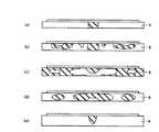
図12は天板の厚さに依存する電界強度分布を示す図である。図12(a)は天板4の面方向の厚さが22.8mmのときの電界強度分布を示しており、中心の斜線で示す部分が電界強度の強くなっている部分である。図12(b)は天板4の厚さを27.8mmにしたときの電界強度分布を示しており、図12(a)に比べて電界強度分布が中心から周辺に広がってきている。図12(c)は天板4の厚さを31.6mmにしたときの電界強度分布を示しており、電界強度分布が天板4の中心部分を除いて周辺まで分布しており、最も適した厚さになっている。図12(d)は天板4の厚さを32.8mmにしたときの電界強度分布を示しており、電界強度分布が中心部のみ強くなっている。図12(e)は天板4の厚さを37.8mmにしたときの電界強度分布を示しており、中心部の電界強度が強くなっている。 FIG. 12 is a diagram showing an electric field intensity distribution depending on the thickness of the top plate. FIG. 12A shows the electric field strength distribution when the thickness of the
図11に示したプラズマ処理装置において、チャンバー1内の圧力やマイクロ波の電力などのプラズマ条件を変更させるとプラズマ表面近傍の電子密度が変化するため、プラズマが物質に侵入する侵入深さが変化する。圧力を低下させると拡散係数が増大するため、プラズマ表面付近の電子密度が低下して侵入深さが増加する。このようにプラズマ条件を変更すると誘電体の適切な厚さが変わるため、定在波を形成するための共振領域がずれてしまう。このため、常に最適な状態でプラズマを発生するためには、プラズマ条件に応じた種々の厚さを有する誘電体を用意しておく必要があるという問題があった。また、マイクロ波は低圧力でのプラズマへの吸収効率が悪く、低圧(20mTorr)でのプラズマの安定した生成が困難になる。 In the plasma processing apparatus shown in FIG. 11, when the plasma conditions such as the pressure in the
それゆえに、この発明の目的は、プラズマ条件に応じて天板内に最適な共振領域を形成し、高い圧力から低い圧力にわたってチャンバー内に安定したプラズマの発生が可能なプラズマ処理装置を提供することである。 SUMMARY OF THE INVENTION Therefore, an object of the present invention is to provide a plasma processing apparatus in which an optimum resonance region is formed in the top plate according to plasma conditions, and stable plasma can be generated in the chamber from high pressure to low pressure. It is.
この発明は、被処理基板を収納し、プラズマを発生するプラズマ発生室と、プラズマ発生室の上部の開口部に配置され、マイクロ波によって駆動されて電磁界を発生するアンテナと、アンテナの下部に設けられて面方向に均一な所定の厚さを有してプラズマ発生室の開口部を封止する天板と、天板の下面側に形成されたテーパ状の凸部または凹部とを備えたことを特徴とする。 The present invention includes a plasma generation chamber for storing a substrate to be processed and generating plasma, an antenna disposed in an upper opening of the plasma generation chamber and driven by microwaves to generate an electromagnetic field, and a lower portion of the antenna. A top plate that is provided and has a uniform predetermined thickness in the surface direction and seals the opening of the plasma generation chamber; and a tapered convex portion or a concave portion formed on the lower surface side of the top plate. It is characterized by that.
この発明では、天板に形成した凸部または凹部のテーパ状部分により、径方向の厚さを連続的に変化させて、プラズマのどの条件においてもどこかで共振させて最適な共振領域を形成できる。したがって、1種類の天板を用意するだけで種々の厚さの天板を用意したのと同様の効果を奏することができる。これにより、プラズマへの吸収効率を飛躍的に向上させることができ、高い圧力から低い圧力にわたって安定したプラズマの発生が可能になる。 According to the present invention, the thickness of the radial direction is continuously changed by the convex portion or the tapered portion of the concave portion formed on the top plate, and an optimum resonance region is formed by resonating somewhere under any plasma conditions. it can. Therefore, it is possible to obtain the same effect as that of preparing various types of top plates only by preparing one type of top plate. As a result, the absorption efficiency into the plasma can be dramatically improved, and stable plasma can be generated from a high pressure to a low pressure.
好ましくは、天板は凸部または凹部により肉厚の薄い部分と厚い部分とを含み、肉厚の薄い部分の厚みはλ/4±λ/8に選ばれている。 Preferably, the top plate includes a thin part and a thick part by a convex part or a concave part, and the thickness of the thin part is selected to be λ / 4 ± λ / 8.
好ましくは、凸部または凹部は、天板の下面にリング状に形成される突条を含む。 Preferably, the convex portion or the concave portion includes a protrusion formed in a ring shape on the lower surface of the top plate.
好ましくは、天板は円板状であって、突条は天板の中心と同心的に径方向に複数形成される。 Preferably, the top plate has a disc shape, and a plurality of ridges are formed concentrically with the center of the top plate in the radial direction.
好ましくは、突条は天板側の径方向厚さが先端側の径方向厚さよりも厚く形成される。 Preferably, the protrusion is formed such that the radial thickness on the top plate side is thicker than the radial thickness on the distal end side.
好ましくは、凸部または凹部は、天板の下面に形成される円錘状の突起を含む。 Preferably, the convex portion or the concave portion includes a conical protrusion formed on the lower surface of the top plate.
好ましくは、円錐状の突起は、天板の中心下面に形成される。 Preferably, the conical protrusion is formed on the lower center surface of the top plate.
好ましくは、円錐状の突起は複数設けられ、複数の円錐状の突起はリング状に配置される。 Preferably, a plurality of conical protrusions are provided, and the plurality of conical protrusions are arranged in a ring shape.
好ましくは、凸部または凹部は、複数のリング状の凹部と、複数のリング状凹部の間に形成される下向きの第1の突条と、最外周のリング状凹部の外側に形成される下向きの第2の突条とを含む。 Preferably, the convex portion or the concave portion has a plurality of ring-shaped concave portions, a downward first protrusion formed between the plurality of ring-shaped concave portions, and a downward direction formed outside the outermost ring-shaped concave portion. And the second protrusion.
好ましくは、第2の凸部の肉厚は、第1の凸部の肉厚に比べて厚く形成される。 Preferably, the thickness of the second convex portion is formed thicker than the thickness of the first convex portion.
好ましくは、天板のアンテナ側の中心部には凹部が形成されており、凹部には天板の誘電率と異なる物質が配置される。 Preferably, a recess is formed in the center of the top plate on the antenna side, and a substance having a dielectric constant different from that of the top plate is disposed in the recess.
好ましくは、天板の凹部の深さはλ/8以上の深さに形成される。 Preferably, the depth of the concave portion of the top plate is formed to a depth of λ / 8 or more.
好ましくは、天板の凹部の深さはλ/4以上の深さに形成される。 Preferably, the depth of the concave portion of the top plate is formed to a depth of λ / 4 or more.
好ましくは、天板の被処理基板側の中心部には凸部が形成され、凸部の周辺における天板の肉厚はλ/4±λ/8である。 Preferably, a convex portion is formed at the center of the top plate on the side of the substrate to be processed, and the thickness of the top plate around the convex portion is λ / 4 ± λ / 8.
好ましくは、被処理基板は円板状であって、凸部または凹部は、被処理基板の半径をRとしたとき、天板の中心から半径Rより外側に少なくとも1つ形成されている。 Preferably, the substrate to be processed is disk-shaped, and at least one convex portion or recess is formed outside the radius R from the center of the top plate, where R is the radius of the substrate to be processed.
好ましくは、凸部または凹部は、天板と処理基板との距離をDとしたとき、天板の中心から半径Dより内側に少なくとも1つ形成されている。 Preferably, at least one protrusion or recess is formed inside the radius D from the center of the top plate, where D is the distance between the top plate and the processing substrate.
好ましくは、アンテナは、面上にスロットが分布して形成されたスロット板を含み、天板にはスロット板上のスロットの位置に対応して凸部または凹部が形成される。 Preferably, the antenna includes a slot plate in which slots are distributed on the surface, and a convex portion or a concave portion is formed on the top plate corresponding to the position of the slot on the slot plate.
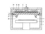
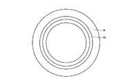
図1はこの発明の一実施形態におけるプラズマ処理装置の断面図であり、図2は図1に示した誘電板を下面から見た図である。 FIG. 1 is a cross-sectional view of a plasma processing apparatus according to an embodiment of the present invention, and FIG. 2 is a view of the dielectric plate shown in FIG.
プラズマ処理装置は、前述の図11と同様にして、基板11を収容して基板11に所定の処理を施すためのチャンバー1と、マイクロ波をチャンバー1内に放射するためのアンテナ部3とを備えている。 In the same manner as in FIG. 11 described above, the plasma processing apparatus includes a
図示しない高周波電源によって発生されたマイクロ波は、導波管6によりアンテナ部3へ送られる。チャンバー1の上部には、チャンバー1の開口部を封止しかつチャンバー1の隔壁の一部を構成する天板4が配設されており、天板4とチャンバー1の隔壁との間には例えばOリングなどのシール部材14が設けられている。アンテナ部3はこの天板4の上方に配置されている。アンテナ部3の上部には内部に冷媒が流れる冷却プレート10が設けられている。 Microwaves generated by a high-frequency power source (not shown) are sent to the
チャンバー1内には、収納された基板11を保持するためのサセプタ7が設けられている。サセプタ7は基板11を加熱するためのヒータ機能を有している。さらに、チャンバー1には、チャンバー1内を排気するために、図11に示した真空ポンプが接続されている。この真空ポンプによってチャンバー1内が排気されて、所定の圧力範囲の下でプラズマを生成するためのガスとして例えばアルゴンガスがチャンバー1内に導入される。 In the
上述のプラズマ装置では、高周波電源により発生したマイクロ波が導波管6を伝わり、アンテナ部3に到達する。アンテナ部3に到達したマイクロ波は遅波板3bを伝播し、スロット板3cを介して天板4に共振領域を形成し、定在波を発生させてチャンバー1内に電磁界を発生させる。チャンバー1内に発生した電磁界によってアルゴンガスが解離し、基板11と天板4との間にプラズマ生成領域22が形成されて、基板11に所定のプラズマ処理が行われる。 In the plasma apparatus described above, the microwave generated by the high frequency power source is transmitted through the
天板4は強度を確保して外気が押す力に対抗するために面方向に均一な所定の厚さを有する円板状に形成されており、その下面には凸部または凹部が形成されている。より具体的には、凸部または凹部として、天板4の周縁から径方向に所定の間隔を隔てて、周辺部に天板4の中心と同心的にリング状の突条41が形成されている。この突条41は外周面が天板4の下面に対して垂直であり、内周面が天板4に対して所定の角度を有するようにテーパ状に形成されて断面が矩形の凸部または凹部を形成している。天板4の周辺部に突条41を形成するのは、天板4にはアンテナ部3からマイクロ波が供給されており、中心部のプラズマ密度が密になっているのに対して、周辺部では疎になっており、周辺部のプラズマ密度を高めるためである。 The
図3は天板内をマイクロ波が伝播する状態を説明するための図である。天板4は突条41により肉厚の厚い部分と、それ以外の肉厚の薄い部分とが含まれているが、肉厚の薄い部分の厚みをλ/4±λ/8に選ぶことにより、マイクロ波が天板4の肉厚の薄い部分で伝播しにくくなる。 FIG. 3 is a diagram for explaining a state in which microwaves propagate through the top plate. The
その理由について説明すると、天板内を通過する電磁波の形態には、モードAとモードBとが存在する。モードAは電子密度が所定値以上になると存在し、モードBは電子密度が比較的小さい場合のみ存在するので、ある程度電子密度が高いときにはモードBによるマイクロ波伝播は抑制される。 The reason will be described. Mode A and mode B exist in the form of electromagnetic waves passing through the top plate. Mode A exists when the electron density exceeds a predetermined value, and mode B exists only when the electron density is relatively low. Therefore, microwave propagation by mode B is suppressed when the electron density is high to some extent.
ただし、これは天板厚みに大きく依存し、λ/4以上の厚みでは、厚くなるほどモードBでの伝播を抑制できる電子密度の下限が高くなってしまう。λ/2以上になると、電子密度に依存せずにモードBが存在することができるようになるので、モードBでの伝播は抑制できなくなる。逆に、λ/4以下では、モードBでの伝播を抑制できる電子密度の下限は変わらない。したがって、天板の強度を考慮するとλ/4が最適となる。ただし、±λ/8の範囲であれば、大方モードBでの伝播を抑制できることになる。 However, this greatly depends on the thickness of the top plate. At a thickness of λ / 4 or more, the lower the electron density that can suppress propagation in mode B, the higher the thickness. If it becomes λ / 2 or more, the mode B can exist without depending on the electron density, so that the propagation in the mode B cannot be suppressed. On the other hand, at λ / 4 or less, the lower limit of the electron density that can suppress propagation in mode B does not change. Therefore, λ / 4 is optimal in consideration of the strength of the top plate. However, in the range of ± λ / 8, propagation in the majority mode B can be suppressed.
アンテナ部3に供給されたマイクロ波は、アンテナ部3のスロットから下方向に放射されるが、図3に示すように天板4内で反射され、それが天板4内の反射の繰り返しで面方向に振動して共振領域を形成して定在波となる。(肉厚の薄い部分で伝播しにくいという説明でありながら図3においてマイクロ波が径方向に伝播するように図示されており、辻褄が合わないように思われます。補足説明下さい。)突条部41に入ったマイクロ波はプラズマ生成領域22に出難くなるので、突条部分41にマイクロ波が蓄積されやすくなる。これにより、突条41を形成したことによる周辺部のプラズマ密度を高めることができる。突条41部分は天板4の周辺部で共振領域を構成し、マイクロ波が天板4の面方向に直交する径方向に振動する。 The microwaves supplied to the
突条41は天板4側の径方向厚さが厚いのに対して、先端側の径方向厚さが薄くなるようにテーパ状に形成されているので、径方向に振動する振幅と突条41の厚さが一致する部分が必ず存在する。すなわち、突条41は天板4の周辺部に共振領域を構成し、共振領域がプラズマ密度に応じて自動的に上下するので、プラズマのどの条件においてもどこかで共振するところが存在する。 The
これにより天板4に最適な共振領域を形成できるので強い電界を発生させて定在波を形成でき、プラズマ密度を高くでき、高い圧力から低い圧力にわたって安定したプラズマの発生が可能になる。 As a result, an optimal resonance region can be formed on the
なお、この突条41は、外周面側および内周面側ともにテーパ状に形成してもよい。また、天板4の厚さに応じて、突条41を配置する位置あるいは形状を任意に選択すればよい。 In addition, you may form this
前述の特開2002−299240号公報には、ドーム状に形成した天板について記載されているが、ドーム形状の場合は共振場所が半径方向に大きく移動し、プラズマの強い場所が移動し、均一性が変化することになる。これに対して、この発明では突条41により天板4の外周あるいは中心付近にプラズマを集めることによって均一性の調整を行うことができる点において異なっている。 The above-mentioned Japanese Patent Application Laid-Open No. 2002-299240 describes a top plate formed in a dome shape, but in the case of a dome shape, the resonance location moves greatly in the radial direction, the strong plasma location moves, and is uniform. Sex will change. On the other hand, the present invention is different in that the uniformity can be adjusted by collecting plasma on the outer periphery or near the center of the
図4はこの発明の他の実施形態における天板に形成した凸部の変形例を示す断面図である。図4(a)に示した例は、天板4のほぼ中心の下部に凸部としての円錐状の突起42を下向きに形成したものである。この例では、突起42が形成された中心部周辺で共振領域を形成できるので、中心部周辺のプラズマ密度を高くでき、天板4の中心部周辺で電界強度が小さい場合に有効である。 FIG. 4 is a cross-sectional view showing a modification of the convex portion formed on the top plate according to another embodiment of the present invention. In the example shown in FIG. 4A, a
図4(b)に示した例は天板4の周辺にリング状の突条43を形成し、外周面および内周面をともにテーパ状に形成したものである。外周面と内周面とをともにテーパ状に形成することで、突条43の天板側の径方向厚さと先端側の径方向厚さとの差を大きくできるので、突条43の周辺に形成される共振領域を広げることができ、その周辺のプラズマ密度を高くできる。 In the example shown in FIG. 4B, a ring-shaped
図4(c)は図2に示した周辺部の突条41の他に、中心部に径方向の厚さを突条41よりも厚くした円錐状の突起44を形成したものである。この例では、突条41によって周辺部に共振領域を形成するとともに、突起44によって中心部に共振領域を形成することで、突条41の径方向厚さよりも大きな振幅のマイクロ波が入力されても、中央の突起44で共振領域を構成できるので中心部でプラズマ密度を高くできる。 FIG. 4C shows a structure in which, in addition to the
図5はこの発明のさらに他の実施形態における凹部を形成した天板を示す断面図である。図5(a)に示した例は、天板4のほぼ中央部に下向きに開口された円形の凹部401を設けたものである。凹部401は下部の開口径が大きくなるように内周面がテーパ状に形成されている。この凹部401により、その外側には凸部402が形成される。この例では、凸部402の肉厚の厚い部分で共振領域を形成できるので、この部分でのプラズマ密度を高くでき、天板4の周辺部分での電界密度が小さい場合に有効である。 FIG. 5 is a cross-sectional view showing a top plate in which concave portions are formed in still another embodiment of the present invention. In the example shown in FIG. 5A, a circular
図5(b)は天板4と同心的にリング状の凹部403を設けたものである。凹部403の外周面および内周面は下部の開口径が大きくなるようにテーパ状に形成されている。この凹部403により、その内側には下向きの凸部404が形成され、その外側には突条405が形成される。この例では、凸部404と突条405の肉厚の厚い部分で共振領域を形成できるので、これらの部分でのプラズマ密度を高くできる。 FIG. 5B is a view in which a ring-shaped
図5(c)は天板4のほぼ中央部に下向きに開口された円形の凹部406と、凹部406の外側にリング状の凹部407とを形成したものである。凹部406は下部の開口径が大きくなるように外周面がテーパ状に形成されており、凹部407は図5(b)の凹部403と同様にして、外周面および内周面は下部の開口径が大きくなるようにテーパ状に形成されている。この例では、凹部406の外側に突条408が形成され、凹部407の外側に突条409が形成され、突条408と409の肉厚の厚い部分で共振領域を形成できるので、これらの部分でのプラズマ密度を高くできる。 FIG. 5C shows a circular
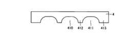
図6はこの発明のさらに他の実施形態における天板に形成した凹部の変形例を示す断面図である。この実施形態は、図5(c)に示した例における凹部406とリング状の凹部407に代えて、凹部410とリング状の凹部411とを形成したものである。凹部410と411は下向きに開口されているが、凹部410の外周面はテーパ状ではなく円弧状に形成されており、凹部411の外周面および内周面も円弧状に形成されている。したがって、この発明におけるテーパ状には円弧状も含まれるものとする。 FIG. 6 is a cross-sectional view showing a modification of the concave portion formed in the top plate according to still another embodiment of the present invention. In this embodiment, a
このように天板4の厚みが円弧状に変化するように形成することで図5(c)と同様にして、凹部410およびリング状の凹部411の間に突条412が形成され、凹部411の外側に突条413が形成され、これらの肉厚の厚い部分で共振領域を形成できるので、これらの部分でのプラズマ密度を高くできる。 By forming the
なお、図1〜図6に示した実施形態において、天板4に形成するテーパ状部は、図7に示すように基板11の半径Rよりも外側に少なくとも1つ形成するのが望ましい。これにより、基板11の端部付近でのプラズマ密度が過度に低くならないようにすることができる。 In the embodiment shown in FIGS. 1 to 6, it is desirable to form at least one tapered portion formed on the
さらに、より好ましくは、天板4に形成するテーパ状部は、図7に示した天板4と基板11との間の距離をDとすると、天板4の中心から半径Dよりも内側に少なくとも1つ形成されているのが望ましい。これにより、天板4の中心付近のプラズマが過度に低くならないようにすることができる。 More preferably, the tapered portion formed on the
図8はこの発明のさらに他の実施形態における天板に形成した凹部の変形例を示す断面図である。図8(a)に示した例は、天板4の中心部に下向きに突出する凸部421を形成し、この凸部421の外側付近の天板4の厚みはλ/4±λ/8に選ばれている。さらに、凸部421の外側には、下向きに開口されたリング状の凹部422を形成するとともに、凹部422の外側に、下向きに突出する肉厚の厚い凸部423を形成し、凸部423の外周部を除いて下面に同心的に複数のリング状の溝424を形成する。凸部421の外周面と、凸部423の内周面はテーパ状に形成されている。 FIG. 8 is a cross-sectional view showing a modification of the recess formed in the top plate according to still another embodiment of the present invention. In the example shown in FIG. 8A, a
この例では、凹部422の外側に肉厚の厚い凸部423を形成したことにより強度を高めることができる。また、この凸部423部分でのプラズマ密度が高くなり電界密度も高くなってプラズマが放射しやすくなるが、複数のリング状の溝424によりその表面からプラズマが放射されるのを抑制でき、溝424が形成されていない最外周部からプラズマを放射しやすくなる。 In this example, the strength can be increased by forming the thick
さらに、天板4のアンテナ3側である大気側には凹部425が形成されている。この凹部425は、その深さがλ/8以上に形成されており、より好ましくはλ/4以上に形成されるのが好ましい。凹部425には大気,良導体もしくは天板4とは誘電率の異なる物質(図示せず)が配置される。これはマイクロ波が天板4の中心部の凹部425付近で強く反射されるので、この部分でプラズマが強くなりがちであるという問題点を改善するためである。凹部425の周辺部の肉厚がλ/4近傍であれば、さらにその効果が助長される。 Further, a
なお、凹部425は天板4のアンテナ3側の中心部に限らず周辺に形成してもよい。 The
図8(b)に示した例は、天板4の中心部の下部に突出する凸部421を形成し、凸部421の外側に下部が開口されたリング状の凹部422を形成し、凹部422の外側に突条426を下向きに形成し、さらに突条426の外側に下部が開口されたリング状の凹部427を形成し、凹部427の外側に下向きに突出するリング状の突条428を形成したものである。最外周に形成された突条428は凸部421および突条426に比べて肉厚が厚く形成されている。また、凹部422および427の外周面および内周面はテーパ状に形成されている。 In the example shown in FIG. 8B, a
この例では、突条426を形成したことにより、天板4の機械的強度を保つことができる。また、突条426と428とで共振領域が形成されるが、突条426に比べて最外周の突条428部分の肉厚が厚く形成されていることにより、この部分でのプラズマ密度を突条426のプラズマ密度に比べて高くできる。 In this example, the mechanical strength of the
図8(c)に示した例では、天板4の中央部に下向きに円板状の凸部429を形成し、その下面に同心的に複数の溝430を形成し、凸部429の外側に下向きに開口されたリング状の凹部431を形成し、凹部431の外側に下向きに突出する突条432を形成したものである。突条432は凸部429に比べて肉厚が厚く形成されている。この例では、天板4の中央部の凸部429により肉厚を厚くして機械的強度を高めることができる。凸部429は肉厚が厚いためプラズマが伝播しやすくなり、密度が高くなるが溝430が形成されていることによりプラズマが放射され難くなる。そして、凹部431の肉厚の薄い部分ではプラズマが伝播しにくくなり、最外周部の突条432でのプラズマ密度を高くできる。なお、この例においても、図8(a)と同様にして、天板4のアンテナ3側である大気側には凹部425が形成されている。 In the example shown in FIG. 8C, a disk-shaped
図9はこの発明の他の実施形態として、スロット板のスロットの位置に対応して突条を形成したものである。すなわち、図9(a)に示すように円板状のスロット板3cには同心円上に三重にリング状に配列されたスロット31,32,33が形成されている。導波管6に入力されるマイクロ波は、スロット板3cのスロット31,32,33を介してチャンバー1内に放射されて電磁界が発生される。したがって、天板4のうちスロット31,32,33の位置に対応する部分の電界強度が最も大きくなっている。 FIG. 9 shows another embodiment of the present invention in which protrusions are formed corresponding to the slot positions of the slot plate. That is, as shown in FIG. 9A,
そこで、図9(b)に示すように各スロット31,32,33の各位置に対応してリング状の複数の突条45,46,47が形成される。これらの突条45,46,47は、図1に示した突条41と同様にして外周面が天板4の下面に対して垂直であり、内周面が天板4に対して所定の角度を有するようにテーパ状に形成されているが、外周面側もテーパ状に形成してもよい。天板4のうち各スロット31,32,33の各位置に対応する部分の電界強度が強くなっており、この部分に共振領域を形成することでプラズマを均一にさせることができる。 Therefore, as shown in FIG. 9B, a plurality of ring-shaped
図10はこの発明のさらに他の実施形態を示す天板を下から見た図である。前述の図9(b)に示した実施形態は、スロット板3cの各スロット31,32,33の位置に対応してリング状の突条45,46,47を形成したのに対して、この実施形態では、各スロット31,32,33の各位置に対応してそれぞれが独立しかつ径の小さな円錘状の突起48を多数配置したものである。この実施形態においても、各スロット31,32,33で生じた強い電界強度を多数の突起48によって共振を分散させることができる。 FIG. 10 is a view of a top plate showing still another embodiment of the present invention as viewed from below. In the embodiment shown in FIG. 9B, ring-shaped
本件発明において、天板4の厚さが21mmで、天板4の直径が280mmで、突条41の直径が220mmで突出高さを22mmに形成したとき、プラズマ条件としての、例えばプラズマの圧力が1〜100Torrに変化し、マイクロ波の出力が100〜3000W変化したときでも安定したプラズマを発生できる。 In the present invention, when the
図面を参照してこの発明の一実施形態を説明したが、本発明は、図示した実施形態に限定されるものではない。本発明と同一の範囲内において、または均等の範囲内において、図示した実施形態に対して種々の変更を加えることが可能である。 Although one embodiment of the present invention has been described with reference to the drawings, the present invention is not limited to the illustrated embodiment. Various modifications can be made to the illustrated embodiment within the same scope or equivalent scope as the present invention.
マイクロ波によって駆動されて電磁界を発生するアンテナ部3の下部にチャンバー1の開口部を封止する天板4を設け、天板4の下面側にリング状の突条41を設けて径方向の厚さをテーパ状に連続的に変化させ、プラズマのどの条件においてもどこかで共振させることにより、高い圧力から低い圧力にわたって安定したプラズマの発生が可能なプラズマ処理装置に利用できる。 A
1 チャンバー、3 アンテナ部、3b 遅波板、3c スロット板、4 天板、6 導波管、7 サセプタ、10 冷却プレート、11 基板、22 プラズマ生成領域、31〜33 スロット、41,43,45〜47,405,408,409,412,413,426,428,432 突条、42,44,48 突起、401,403,406,407,410,411,422,425,427,431 凹部、402,404,408,413,421,423,429 凸部、424,430 溝。 1 chamber, 3 antenna section, 3b slow wave plate, 3c slot plate, 4 top plate, 6 waveguide, 7 susceptor, 10 cooling plate, 11 substrate, 22 plasma generation region, 31-33 slot, 41, 43, 45 ~ 47,405,408,409,412,413,426,428,432 protrusion, 42,44,48 protrusion, 401,403,406,407,410,411,422,425,427,431 recess, 402 , 404, 408, 413, 421, 423, 429 Protrusions, 424, 430 grooves.
Claims (18)
Translated fromJapanese前記プラズマ発生室の上部の開口部に配置され、マイクロ波によって駆動されて電磁界を発生するアンテナと、
前記アンテナの下部に設けられ、面方向に渡って均一な所定の厚さを有して前記プラズマ発生室の開口部を封止する天板と、
前記天板の下面側に形成されるテーパ状部とを備え、
前記テーパ状部の先端側、および前記テーパ状部の天板側に位置する前記天板の下面側の両方には、平面が形成されている、プラズマ処理装置。A plasma generation chamber for storing a substrate to be processed and generating plasma;
An antenna that is disposed in an opening at the top of the plasma generation chamber and is driven by microwaves to generate an electromagnetic field;
A top plate provided at a lower portion of the antenna and having a predetermined thickness that is uniform in a plane direction and sealing the opening of the plasma generation chamber;
A tapered portion formed on the lower surface side of the top plate,
A plasma processing apparatus, wherein a flat surface is formed on both the distal end side of the tapered portion and the lower surface side of the top plate located on the top plate side of the tapered portion .
前記リング状の突条は、前記天板の中心と同心的に径方向に複数形成される、請求項3に記載のプラズマ処理装置。The top plate is disc-shaped,
The plasma processing apparatus according to claim 3, wherein a plurality of the ring-shaped protrusions are formed in a radial direction concentrically with a center of the top plate.
前記テーパ状部は、前記被処理基板の半径をRとしたとき、前記天板の中心から半径Rより外側に少なくとも1つ形成されている、請求項4、5、7から9のいずれかに記載のプラズマ処理装置。The substrate to be processed is disk-shaped,
Thetaper-shaped portion is formed at least one outside the radius R from the center of the top plate, where R is a radius of the substrate to be processed, according to any one of claims 4, 5, 7 to 9. The plasma processing apparatus as described.
前記天板の下面の前記テーパ状部は、前記所定のパターンに対応する位置に延在するように形成されている、請求項1から5のいずれかに記載のプラズマ処理装置。The antenna includes a slot plate formed such that a plurality of slots are distributed in a predetermined pattern,
The plasma processing apparatus according to claim 1, wherein thetapered portion on the lower surface of the top plate is formed to extend to a position corresponding to the predetermined pattern.
Priority Applications (6)
| Application Number | Priority Date | Filing Date | Title |
|---|---|---|---|
| JP2004159186AJP4563729B2 (en) | 2003-09-04 | 2004-05-28 | Plasma processing equipment |
| TW101143844ATWI436697B (en) | 2003-09-04 | 2004-09-03 | Plasma processing device |
| KR1020067002758AKR100824813B1 (en) | 2003-09-04 | 2004-09-03 | Plasma processing equipment |
| TW093126710ATWI454186B (en) | 2003-09-04 | 2004-09-03 | Plasma processing device |
| PCT/JP2004/012824WO2005031830A1 (en) | 2003-09-04 | 2004-09-03 | Plasma processing device |
| US10/570,631US7930992B2 (en) | 2003-09-04 | 2004-09-03 | Plasma processing equipment |
Applications Claiming Priority (2)
| Application Number | Priority Date | Filing Date | Title |
|---|---|---|---|
| JP2003312486 | 2003-09-04 | ||
| JP2004159186AJP4563729B2 (en) | 2003-09-04 | 2004-05-28 | Plasma processing equipment |
Related Child Applications (1)
| Application Number | Title | Priority Date | Filing Date |
|---|---|---|---|
| JP2010129799ADivisionJP2010258461A (en) | 2003-09-04 | 2010-06-07 | Plasma processing apparatus and top plate for plasma processing apparatus |
Publications (3)
| Publication Number | Publication Date |
|---|---|
| JP2005100931A JP2005100931A (en) | 2005-04-14 |
| JP2005100931A5 JP2005100931A5 (en) | 2007-07-05 |
| JP4563729B2true JP4563729B2 (en) | 2010-10-13 |
Family
ID=34395578
Family Applications (1)
| Application Number | Title | Priority Date | Filing Date |
|---|---|---|---|
| JP2004159186AExpired - Fee RelatedJP4563729B2 (en) | 2003-09-04 | 2004-05-28 | Plasma processing equipment |
Country Status (5)
| Country | Link |
|---|---|
| US (1) | US7930992B2 (en) |
| JP (1) | JP4563729B2 (en) |
| KR (1) | KR100824813B1 (en) |
| TW (2) | TWI454186B (en) |
| WO (1) | WO2005031830A1 (en) |
Families Citing this family (346)
| Publication number | Priority date | Publication date | Assignee | Title |
|---|---|---|---|---|
| US8267040B2 (en) | 2004-02-16 | 2012-09-18 | Tokyo Electron Limited | Plasma processing apparatus and plasma processing method |
| JP4953153B2 (en)* | 2005-07-28 | 2012-06-13 | 住友電気工業株式会社 | Microwave plasma CVD equipment |
| JP4756540B2 (en)* | 2005-09-30 | 2011-08-24 | 東京エレクトロン株式会社 | Plasma processing apparatus and method |
| JP5082229B2 (en)* | 2005-11-29 | 2012-11-28 | 東京エレクトロン株式会社 | Plasma processing equipment |
| JP5096047B2 (en)* | 2007-06-14 | 2012-12-12 | 東京エレクトロン株式会社 | Microwave plasma processing apparatus and microwave transmission plate |
| WO2009028376A1 (en) | 2007-08-28 | 2009-03-05 | Tokyo Electron Limited | Top panel and plasma processing apparatus |
| JP5374853B2 (en)* | 2007-10-17 | 2013-12-25 | 東京エレクトロン株式会社 | Plasma processing equipment |
| US20100307685A1 (en)* | 2008-01-31 | 2010-12-09 | Tokyo Electron Limited | Microwave plasma processing apparatus |
| KR101114848B1 (en)* | 2008-02-08 | 2012-03-07 | 도쿄엘렉트론가부시키가이샤 | plasma processing apparatus and plasma processing method |
| JP5407388B2 (en)* | 2008-02-08 | 2014-02-05 | 東京エレクトロン株式会社 | Plasma processing equipment |
| US8753475B2 (en) | 2008-02-08 | 2014-06-17 | Tokyo Electron Limited | Plasma processing apparatus |
| JP5369733B2 (en)* | 2008-02-27 | 2013-12-18 | 東京エレクトロン株式会社 | Plasma processing equipment |
| KR101157143B1 (en)* | 2008-02-13 | 2012-06-22 | 도쿄엘렉트론가부시키가이샤 | Top board of microwave plasma processing device, plasma processing device and plasma processing method |
| JP4585574B2 (en)* | 2008-02-26 | 2010-11-24 | 東京エレクトロン株式会社 | Plasma processing apparatus and plasma processing method |
| WO2009107718A1 (en) | 2008-02-27 | 2009-09-03 | 東京エレクトロン株式会社 | Plasma etching apparatus and plasma etching method |
| KR20090102955A (en)* | 2008-03-27 | 2009-10-01 | 주식회사 유진테크 | Apparatus and method for processing substrate |
| JP5243089B2 (en)* | 2008-04-09 | 2013-07-24 | 東京エレクトロン株式会社 | Seal structure of plasma processing apparatus, sealing method, and plasma processing apparatus |
| US8097082B2 (en)* | 2008-04-28 | 2012-01-17 | Applied Materials, Inc. | Nonplanar faceplate for a plasma processing chamber |
| JP2009302181A (en)* | 2008-06-11 | 2009-12-24 | Tokyo Electron Ltd | Plasma etching method, and plasma etching apparatus |
| KR20100002532A (en)* | 2008-06-30 | 2010-01-07 | 삼성전자주식회사 | Apparatus for processing a substrate |
| US8800484B2 (en) | 2008-07-09 | 2014-08-12 | Tokyo Electron Limited | Plasma processing apparatus |
| US8242405B2 (en)* | 2008-07-15 | 2012-08-14 | Tokyo Electron Limited | Microwave plasma processing apparatus and method for producing cooling jacket |
| KR101239772B1 (en)* | 2009-02-06 | 2013-03-06 | 도쿄엘렉트론가부시키가이샤 | Plasma processing device |
| JP2010232493A (en)* | 2009-03-27 | 2010-10-14 | Tokyo Electron Ltd | Plasma processing device |
| US9394608B2 (en) | 2009-04-06 | 2016-07-19 | Asm America, Inc. | Semiconductor processing reactor and components thereof |
| US8802201B2 (en) | 2009-08-14 | 2014-08-12 | Asm America, Inc. | Systems and methods for thin-film deposition of metal oxides using excited nitrogen-oxygen species |
| US8415884B2 (en)* | 2009-09-08 | 2013-04-09 | Tokyo Electron Limited | Stable surface wave plasma source |
| JP5670245B2 (en)* | 2011-04-06 | 2015-02-18 | 株式会社アルバック | Plasma processing equipment |
| JP5377587B2 (en)* | 2011-07-06 | 2013-12-25 | 東京エレクトロン株式会社 | Antenna, plasma processing apparatus, and plasma processing method |
| US20130023129A1 (en) | 2011-07-20 | 2013-01-24 | Asm America, Inc. | Pressure transmitter for a semiconductor processing environment |
| US9017481B1 (en) | 2011-10-28 | 2015-04-28 | Asm America, Inc. | Process feed management for semiconductor substrate processing |
| JP5527490B2 (en)* | 2011-11-11 | 2014-06-18 | 東京エレクトロン株式会社 | Dielectric window for plasma processing apparatus and plasma processing apparatus |
| US8664125B2 (en) | 2011-12-23 | 2014-03-04 | Tokyo Electron Limited | Highly selective spacer etch process with reduced sidewall spacer slimming |
| US9984906B2 (en)* | 2012-05-25 | 2018-05-29 | Tokyo Electron Limited | Plasma processing device and plasma processing method |
| US10714315B2 (en) | 2012-10-12 | 2020-07-14 | Asm Ip Holdings B.V. | Semiconductor reaction chamber showerhead |
| JP2014112644A (en)* | 2012-11-06 | 2014-06-19 | Tokyo Electron Ltd | Plasma processing apparatus and plasma processing method |
| US20160376700A1 (en) | 2013-02-01 | 2016-12-29 | Asm Ip Holding B.V. | System for treatment of deposition reactor |
| JP2015018685A (en)* | 2013-07-10 | 2015-01-29 | 東京エレクトロン株式会社 | Microwave plasma treatment apparatus |
| JP2015130325A (en)* | 2013-12-03 | 2015-07-16 | 東京エレクトロン株式会社 | Dielectric window, antenna, and plasma processing apparatus |
| US11015245B2 (en) | 2014-03-19 | 2021-05-25 | Asm Ip Holding B.V. | Gas-phase reactor and system having exhaust plenum and components thereof |
| US9947516B2 (en)* | 2014-06-03 | 2018-04-17 | Tokyo Electron Limited | Top dielectric quartz plate and slot antenna concept |
| US10858737B2 (en) | 2014-07-28 | 2020-12-08 | Asm Ip Holding B.V. | Showerhead assembly and components thereof |
| US9890456B2 (en) | 2014-08-21 | 2018-02-13 | Asm Ip Holding B.V. | Method and system for in situ formation of gas-phase compounds |
| US10941490B2 (en) | 2014-10-07 | 2021-03-09 | Asm Ip Holding B.V. | Multiple temperature range susceptor, assembly, reactor and system including the susceptor, and methods of using the same |
| JP6406631B2 (en)* | 2014-10-22 | 2018-10-17 | パナソニックIpマネジメント株式会社 | Plasma processing equipment |
| JP2016086099A (en) | 2014-10-27 | 2016-05-19 | 東京エレクトロン株式会社 | Plasma processing apparatus |
| JPWO2016098582A1 (en)* | 2014-12-15 | 2017-11-02 | 東京エレクトロン株式会社 | Plasma processing equipment |
| US9673059B2 (en) | 2015-02-02 | 2017-06-06 | Tokyo Electron Limited | Method for increasing pattern density in self-aligned patterning integration schemes |
| US9443731B1 (en) | 2015-02-20 | 2016-09-13 | Tokyo Electron Limited | Material processing to achieve sub-10nm patterning |
| US10276355B2 (en) | 2015-03-12 | 2019-04-30 | Asm Ip Holding B.V. | Multi-zone reactor, system including the reactor, and method of using the same |
| JP6479550B2 (en)* | 2015-04-22 | 2019-03-06 | 東京エレクトロン株式会社 | Plasma processing equipment |
| US10458018B2 (en) | 2015-06-26 | 2019-10-29 | Asm Ip Holding B.V. | Structures including metal carbide material, devices including the structures, and methods of forming same |
| KR102334378B1 (en) | 2015-09-23 | 2021-12-02 | 삼성전자 주식회사 | Dielectric window, plasma processing system comprising the window, and method for fabricating semiconductor device using the system |
| US10211308B2 (en) | 2015-10-21 | 2019-02-19 | Asm Ip Holding B.V. | NbMC layers |
| US11139308B2 (en) | 2015-12-29 | 2021-10-05 | Asm Ip Holding B.V. | Atomic layer deposition of III-V compounds to form V-NAND devices |
| US10529554B2 (en) | 2016-02-19 | 2020-01-07 | Asm Ip Holding B.V. | Method for forming silicon nitride film selectively on sidewalls or flat surfaces of trenches |
| US10343920B2 (en) | 2016-03-18 | 2019-07-09 | Asm Ip Holding B.V. | Aligned carbon nanotubes |
| US10370763B2 (en)* | 2016-04-18 | 2019-08-06 | Tokyo Electron Limited | Plasma processing apparatus |
| US10865475B2 (en) | 2016-04-21 | 2020-12-15 | Asm Ip Holding B.V. | Deposition of metal borides and silicides |
| US10190213B2 (en) | 2016-04-21 | 2019-01-29 | Asm Ip Holding B.V. | Deposition of metal borides |
| US10367080B2 (en) | 2016-05-02 | 2019-07-30 | Asm Ip Holding B.V. | Method of forming a germanium oxynitride film |
| US11453943B2 (en) | 2016-05-25 | 2022-09-27 | Asm Ip Holding B.V. | Method for forming carbon-containing silicon/metal oxide or nitride film by ALD using silicon precursor and hydrocarbon precursor |
| US9859151B1 (en) | 2016-07-08 | 2018-01-02 | Asm Ip Holding B.V. | Selective film deposition method to form air gaps |
| US10612137B2 (en) | 2016-07-08 | 2020-04-07 | Asm Ip Holdings B.V. | Organic reactants for atomic layer deposition |
| KR102532607B1 (en) | 2016-07-28 | 2023-05-15 | 에이에스엠 아이피 홀딩 비.브이. | Substrate processing apparatus and method of operating the same |
| US9887082B1 (en) | 2016-07-28 | 2018-02-06 | Asm Ip Holding B.V. | Method and apparatus for filling a gap |
| US9812320B1 (en) | 2016-07-28 | 2017-11-07 | Asm Ip Holding B.V. | Method and apparatus for filling a gap |
| US10643826B2 (en) | 2016-10-26 | 2020-05-05 | Asm Ip Holdings B.V. | Methods for thermally calibrating reaction chambers |
| US11532757B2 (en) | 2016-10-27 | 2022-12-20 | Asm Ip Holding B.V. | Deposition of charge trapping layers |
| US10714350B2 (en) | 2016-11-01 | 2020-07-14 | ASM IP Holdings, B.V. | Methods for forming a transition metal niobium nitride film on a substrate by atomic layer deposition and related semiconductor device structures |
| US10229833B2 (en) | 2016-11-01 | 2019-03-12 | Asm Ip Holding B.V. | Methods for forming a transition metal nitride film on a substrate by atomic layer deposition and related semiconductor device structures |
| KR102546317B1 (en) | 2016-11-15 | 2023-06-21 | 에이에스엠 아이피 홀딩 비.브이. | Gas supply unit and substrate processing apparatus including the same |
| KR102762543B1 (en)* | 2016-12-14 | 2025-02-05 | 에이에스엠 아이피 홀딩 비.브이. | Substrate processing apparatus |
| US11581186B2 (en) | 2016-12-15 | 2023-02-14 | Asm Ip Holding B.V. | Sequential infiltration synthesis apparatus |
| US11447861B2 (en) | 2016-12-15 | 2022-09-20 | Asm Ip Holding B.V. | Sequential infiltration synthesis apparatus and a method of forming a patterned structure |
| KR102700194B1 (en) | 2016-12-19 | 2024-08-28 | 에이에스엠 아이피 홀딩 비.브이. | Substrate processing apparatus |
| US10269558B2 (en) | 2016-12-22 | 2019-04-23 | Asm Ip Holding B.V. | Method of forming a structure on a substrate |
| US10867788B2 (en) | 2016-12-28 | 2020-12-15 | Asm Ip Holding B.V. | Method of forming a structure on a substrate |
| US11390950B2 (en) | 2017-01-10 | 2022-07-19 | Asm Ip Holding B.V. | Reactor system and method to reduce residue buildup during a film deposition process |
| US10468261B2 (en) | 2017-02-15 | 2019-11-05 | Asm Ip Holding B.V. | Methods for forming a metallic film on a substrate by cyclical deposition and related semiconductor device structures |
| US10529563B2 (en) | 2017-03-29 | 2020-01-07 | Asm Ip Holdings B.V. | Method for forming doped metal oxide films on a substrate by cyclical deposition and related semiconductor device structures |
| KR102457289B1 (en) | 2017-04-25 | 2022-10-21 | 에이에스엠 아이피 홀딩 비.브이. | Method for depositing a thin film and manufacturing a semiconductor device |
| US10770286B2 (en) | 2017-05-08 | 2020-09-08 | Asm Ip Holdings B.V. | Methods for selectively forming a silicon nitride film on a substrate and related semiconductor device structures |
| US10892156B2 (en) | 2017-05-08 | 2021-01-12 | Asm Ip Holding B.V. | Methods for forming a silicon nitride film on a substrate and related semiconductor device structures |
| US10886123B2 (en) | 2017-06-02 | 2021-01-05 | Asm Ip Holding B.V. | Methods for forming low temperature semiconductor layers and related semiconductor device structures |
| US12040200B2 (en) | 2017-06-20 | 2024-07-16 | Asm Ip Holding B.V. | Semiconductor processing apparatus and methods for calibrating a semiconductor processing apparatus |
| US11306395B2 (en) | 2017-06-28 | 2022-04-19 | Asm Ip Holding B.V. | Methods for depositing a transition metal nitride film on a substrate by atomic layer deposition and related deposition apparatus |
| KR20190009245A (en) | 2017-07-18 | 2019-01-28 | 에이에스엠 아이피 홀딩 비.브이. | Methods for forming a semiconductor device structure and related semiconductor device structures |
| US11018002B2 (en) | 2017-07-19 | 2021-05-25 | Asm Ip Holding B.V. | Method for selectively depositing a Group IV semiconductor and related semiconductor device structures |
| US11374112B2 (en) | 2017-07-19 | 2022-06-28 | Asm Ip Holding B.V. | Method for depositing a group IV semiconductor and related semiconductor device structures |
| US10541333B2 (en) | 2017-07-19 | 2020-01-21 | Asm Ip Holding B.V. | Method for depositing a group IV semiconductor and related semiconductor device structures |
| US10590535B2 (en) | 2017-07-26 | 2020-03-17 | Asm Ip Holdings B.V. | Chemical treatment, deposition and/or infiltration apparatus and method for using the same |
| TWI815813B (en) | 2017-08-04 | 2023-09-21 | 荷蘭商Asm智慧財產控股公司 | Showerhead assembly for distributing a gas within a reaction chamber |
| US10692741B2 (en) | 2017-08-08 | 2020-06-23 | Asm Ip Holdings B.V. | Radiation shield |
| US10770336B2 (en) | 2017-08-08 | 2020-09-08 | Asm Ip Holding B.V. | Substrate lift mechanism and reactor including same |
| US11139191B2 (en) | 2017-08-09 | 2021-10-05 | Asm Ip Holding B.V. | Storage apparatus for storing cassettes for substrates and processing apparatus equipped therewith |
| US11769682B2 (en) | 2017-08-09 | 2023-09-26 | Asm Ip Holding B.V. | Storage apparatus for storing cassettes for substrates and processing apparatus equipped therewith |
| US11830730B2 (en) | 2017-08-29 | 2023-11-28 | Asm Ip Holding B.V. | Layer forming method and apparatus |
| US11295980B2 (en) | 2017-08-30 | 2022-04-05 | Asm Ip Holding B.V. | Methods for depositing a molybdenum metal film over a dielectric surface of a substrate by a cyclical deposition process and related semiconductor device structures |
| US11056344B2 (en) | 2017-08-30 | 2021-07-06 | Asm Ip Holding B.V. | Layer forming method |
| KR102491945B1 (en) | 2017-08-30 | 2023-01-26 | 에이에스엠 아이피 홀딩 비.브이. | Substrate processing apparatus |
| KR102401446B1 (en) | 2017-08-31 | 2022-05-24 | 에이에스엠 아이피 홀딩 비.브이. | Substrate processing apparatus |
| KR102630301B1 (en) | 2017-09-21 | 2024-01-29 | 에이에스엠 아이피 홀딩 비.브이. | Method of sequential infiltration synthesis treatment of infiltrateable material and structures and devices formed using same |
| US10844484B2 (en) | 2017-09-22 | 2020-11-24 | Asm Ip Holding B.V. | Apparatus for dispensing a vapor phase reactant to a reaction chamber and related methods |
| US10658205B2 (en) | 2017-09-28 | 2020-05-19 | Asm Ip Holdings B.V. | Chemical dispensing apparatus and methods for dispensing a chemical to a reaction chamber |
| US10403504B2 (en) | 2017-10-05 | 2019-09-03 | Asm Ip Holding B.V. | Method for selectively depositing a metallic film on a substrate |
| US10923344B2 (en) | 2017-10-30 | 2021-02-16 | Asm Ip Holding B.V. | Methods for forming a semiconductor structure and related semiconductor structures |
| US10910262B2 (en) | 2017-11-16 | 2021-02-02 | Asm Ip Holding B.V. | Method of selectively depositing a capping layer structure on a semiconductor device structure |
| US11022879B2 (en) | 2017-11-24 | 2021-06-01 | Asm Ip Holding B.V. | Method of forming an enhanced unexposed photoresist layer |
| WO2019103613A1 (en) | 2017-11-27 | 2019-05-31 | Asm Ip Holding B.V. | A storage device for storing wafer cassettes for use with a batch furnace |
| CN111344522B (en) | 2017-11-27 | 2022-04-12 | 阿斯莫Ip控股公司 | Including clean mini-environment device |
| US20190189398A1 (en)* | 2017-12-14 | 2019-06-20 | Tokyo Electron Limited | Microwave plasma processing apparatus |
| US10872771B2 (en) | 2018-01-16 | 2020-12-22 | Asm Ip Holding B. V. | Method for depositing a material film on a substrate within a reaction chamber by a cyclical deposition process and related device structures |
| KR102695659B1 (en) | 2018-01-19 | 2024-08-14 | 에이에스엠 아이피 홀딩 비.브이. | Method for depositing a gap filling layer by plasma assisted deposition |
| TWI799494B (en) | 2018-01-19 | 2023-04-21 | 荷蘭商Asm 智慧財產控股公司 | Deposition method |
| US11018047B2 (en) | 2018-01-25 | 2021-05-25 | Asm Ip Holding B.V. | Hybrid lift pin |
| USD880437S1 (en) | 2018-02-01 | 2020-04-07 | Asm Ip Holding B.V. | Gas supply plate for semiconductor manufacturing apparatus |
| US11081345B2 (en) | 2018-02-06 | 2021-08-03 | Asm Ip Holding B.V. | Method of post-deposition treatment for silicon oxide film |
| US10896820B2 (en) | 2018-02-14 | 2021-01-19 | Asm Ip Holding B.V. | Method for depositing a ruthenium-containing film on a substrate by a cyclical deposition process |
| WO2019158960A1 (en) | 2018-02-14 | 2019-08-22 | Asm Ip Holding B.V. | A method for depositing a ruthenium-containing film on a substrate by a cyclical deposition process |
| US10731249B2 (en) | 2018-02-15 | 2020-08-04 | Asm Ip Holding B.V. | Method of forming a transition metal containing film on a substrate by a cyclical deposition process, a method for supplying a transition metal halide compound to a reaction chamber, and related vapor deposition apparatus |
| KR102636427B1 (en) | 2018-02-20 | 2024-02-13 | 에이에스엠 아이피 홀딩 비.브이. | Substrate processing method and apparatus |
| US10975470B2 (en) | 2018-02-23 | 2021-04-13 | Asm Ip Holding B.V. | Apparatus for detecting or monitoring for a chemical precursor in a high temperature environment |
| US11473195B2 (en) | 2018-03-01 | 2022-10-18 | Asm Ip Holding B.V. | Semiconductor processing apparatus and a method for processing a substrate |
| US11629406B2 (en) | 2018-03-09 | 2023-04-18 | Asm Ip Holding B.V. | Semiconductor processing apparatus comprising one or more pyrometers for measuring a temperature of a substrate during transfer of the substrate |
| US11114283B2 (en) | 2018-03-16 | 2021-09-07 | Asm Ip Holding B.V. | Reactor, system including the reactor, and methods of manufacturing and using same |
| KR102646467B1 (en) | 2018-03-27 | 2024-03-11 | 에이에스엠 아이피 홀딩 비.브이. | Method of forming an electrode on a substrate and a semiconductor device structure including an electrode |
| US11088002B2 (en) | 2018-03-29 | 2021-08-10 | Asm Ip Holding B.V. | Substrate rack and a substrate processing system and method |
| US11230766B2 (en) | 2018-03-29 | 2022-01-25 | Asm Ip Holding B.V. | Substrate processing apparatus and method |
| KR102501472B1 (en) | 2018-03-30 | 2023-02-20 | 에이에스엠 아이피 홀딩 비.브이. | Substrate processing method |
| KR102600229B1 (en) | 2018-04-09 | 2023-11-10 | 에이에스엠 아이피 홀딩 비.브이. | Substrate supporting device, substrate processing apparatus including the same and substrate processing method |
| TWI811348B (en) | 2018-05-08 | 2023-08-11 | 荷蘭商Asm 智慧財產控股公司 | Methods for depositing an oxide film on a substrate by a cyclical deposition process and related device structures |
| US12025484B2 (en) | 2018-05-08 | 2024-07-02 | Asm Ip Holding B.V. | Thin film forming method |
| US12272527B2 (en) | 2018-05-09 | 2025-04-08 | Asm Ip Holding B.V. | Apparatus for use with hydrogen radicals and method of using same |
| KR20190129718A (en) | 2018-05-11 | 2019-11-20 | 에이에스엠 아이피 홀딩 비.브이. | Methods for forming a doped metal carbide film on a substrate and related semiconductor device structures |
| KR102596988B1 (en) | 2018-05-28 | 2023-10-31 | 에이에스엠 아이피 홀딩 비.브이. | Method of processing a substrate and a device manufactured by the same |
| US11718913B2 (en) | 2018-06-04 | 2023-08-08 | Asm Ip Holding B.V. | Gas distribution system and reactor system including same |
| TWI840362B (en) | 2018-06-04 | 2024-05-01 | 荷蘭商Asm Ip私人控股有限公司 | Wafer handling chamber with moisture reduction |
| US11286562B2 (en) | 2018-06-08 | 2022-03-29 | Asm Ip Holding B.V. | Gas-phase chemical reactor and method of using same |
| US10797133B2 (en) | 2018-06-21 | 2020-10-06 | Asm Ip Holding B.V. | Method for depositing a phosphorus doped silicon arsenide film and related semiconductor device structures |
| KR102568797B1 (en) | 2018-06-21 | 2023-08-21 | 에이에스엠 아이피 홀딩 비.브이. | Substrate processing system |
| TWI873894B (en) | 2018-06-27 | 2025-02-21 | 荷蘭商Asm Ip私人控股有限公司 | Cyclic deposition methods for forming metal-containing material and films and structures including the metal-containing material |
| KR102854019B1 (en) | 2018-06-27 | 2025-09-02 | 에이에스엠 아이피 홀딩 비.브이. | Periodic deposition method for forming a metal-containing material and films and structures comprising the metal-containing material |
| US10612136B2 (en) | 2018-06-29 | 2020-04-07 | ASM IP Holding, B.V. | Temperature-controlled flange and reactor system including same |
| KR102686758B1 (en) | 2018-06-29 | 2024-07-18 | 에이에스엠 아이피 홀딩 비.브이. | Method for depositing a thin film and manufacturing a semiconductor device |
| US10388513B1 (en) | 2018-07-03 | 2019-08-20 | Asm Ip Holding B.V. | Method for depositing silicon-free carbon-containing film as gap-fill layer by pulse plasma-assisted deposition |
| US10755922B2 (en) | 2018-07-03 | 2020-08-25 | Asm Ip Holding B.V. | Method for depositing silicon-free carbon-containing film as gap-fill layer by pulse plasma-assisted deposition |
| US10767789B2 (en) | 2018-07-16 | 2020-09-08 | Asm Ip Holding B.V. | Diaphragm valves, valve components, and methods for forming valve components |
| WO2020017015A1 (en)* | 2018-07-20 | 2020-01-23 | 株式会社日立ハイテクノロジーズ | Plasma processing device |
| US11053591B2 (en) | 2018-08-06 | 2021-07-06 | Asm Ip Holding B.V. | Multi-port gas injection system and reactor system including same |
| US10883175B2 (en) | 2018-08-09 | 2021-01-05 | Asm Ip Holding B.V. | Vertical furnace for processing substrates and a liner for use therein |
| US10829852B2 (en) | 2018-08-16 | 2020-11-10 | Asm Ip Holding B.V. | Gas distribution device for a wafer processing apparatus |
| US11430674B2 (en) | 2018-08-22 | 2022-08-30 | Asm Ip Holding B.V. | Sensor array, apparatus for dispensing a vapor phase reactant to a reaction chamber and related methods |
| US11024523B2 (en) | 2018-09-11 | 2021-06-01 | Asm Ip Holding B.V. | Substrate processing apparatus and method |
| KR102707956B1 (en) | 2018-09-11 | 2024-09-19 | 에이에스엠 아이피 홀딩 비.브이. | Method for deposition of a thin film |
| US11049751B2 (en) | 2018-09-14 | 2021-06-29 | Asm Ip Holding B.V. | Cassette supply system to store and handle cassettes and processing apparatus equipped therewith |
| CN110970344B (en) | 2018-10-01 | 2024-10-25 | Asmip控股有限公司 | Substrate holding apparatus, system comprising the same and method of using the same |
| US11232963B2 (en) | 2018-10-03 | 2022-01-25 | Asm Ip Holding B.V. | Substrate processing apparatus and method |
| KR102592699B1 (en) | 2018-10-08 | 2023-10-23 | 에이에스엠 아이피 홀딩 비.브이. | Substrate support unit and apparatuses for depositing thin film and processing the substrate including the same |
| KR102546322B1 (en) | 2018-10-19 | 2023-06-21 | 에이에스엠 아이피 홀딩 비.브이. | Substrate processing apparatus and substrate processing method |
| KR102605121B1 (en) | 2018-10-19 | 2023-11-23 | 에이에스엠 아이피 홀딩 비.브이. | Substrate processing apparatus and substrate processing method |
| USD948463S1 (en) | 2018-10-24 | 2022-04-12 | Asm Ip Holding B.V. | Susceptor for semiconductor substrate supporting apparatus |
| US12378665B2 (en) | 2018-10-26 | 2025-08-05 | Asm Ip Holding B.V. | High temperature coatings for a preclean and etch apparatus and related methods |
| US11087997B2 (en) | 2018-10-31 | 2021-08-10 | Asm Ip Holding B.V. | Substrate processing apparatus for processing substrates |
| KR102748291B1 (en) | 2018-11-02 | 2024-12-31 | 에이에스엠 아이피 홀딩 비.브이. | Substrate support unit and substrate processing apparatus including the same |
| US11572620B2 (en) | 2018-11-06 | 2023-02-07 | Asm Ip Holding B.V. | Methods for selectively depositing an amorphous silicon film on a substrate |
| US11031242B2 (en) | 2018-11-07 | 2021-06-08 | Asm Ip Holding B.V. | Methods for depositing a boron doped silicon germanium film |
| US10818758B2 (en) | 2018-11-16 | 2020-10-27 | Asm Ip Holding B.V. | Methods for forming a metal silicate film on a substrate in a reaction chamber and related semiconductor device structures |
| US10847366B2 (en) | 2018-11-16 | 2020-11-24 | Asm Ip Holding B.V. | Methods for depositing a transition metal chalcogenide film on a substrate by a cyclical deposition process |
| US12040199B2 (en) | 2018-11-28 | 2024-07-16 | Asm Ip Holding B.V. | Substrate processing apparatus for processing substrates |
| US11217444B2 (en) | 2018-11-30 | 2022-01-04 | Asm Ip Holding B.V. | Method for forming an ultraviolet radiation responsive metal oxide-containing film |
| KR102636428B1 (en) | 2018-12-04 | 2024-02-13 | 에이에스엠 아이피 홀딩 비.브이. | A method for cleaning a substrate processing apparatus |
| US11158513B2 (en) | 2018-12-13 | 2021-10-26 | Asm Ip Holding B.V. | Methods for forming a rhenium-containing film on a substrate by a cyclical deposition process and related semiconductor device structures |
| TWI874340B (en) | 2018-12-14 | 2025-03-01 | 荷蘭商Asm Ip私人控股有限公司 | Method of forming device structure, structure formed by the method and system for performing the method |
| TWI866480B (en) | 2019-01-17 | 2024-12-11 | 荷蘭商Asm Ip 私人控股有限公司 | Methods of forming a transition metal containing film on a substrate by a cyclical deposition process |
| KR102727227B1 (en) | 2019-01-22 | 2024-11-07 | 에이에스엠 아이피 홀딩 비.브이. | Semiconductor processing device |
| CN111524788B (en) | 2019-02-01 | 2023-11-24 | Asm Ip私人控股有限公司 | Method for forming topologically selective films of silicon oxide |
| TWI873122B (en) | 2019-02-20 | 2025-02-21 | 荷蘭商Asm Ip私人控股有限公司 | Method of filling a recess formed within a surface of a substrate, semiconductor structure formed according to the method, and semiconductor processing apparatus |
| TWI845607B (en) | 2019-02-20 | 2024-06-21 | 荷蘭商Asm Ip私人控股有限公司 | Cyclical deposition method and apparatus for filling a recess formed within a substrate surface |
| TWI838458B (en) | 2019-02-20 | 2024-04-11 | 荷蘭商Asm Ip私人控股有限公司 | Apparatus and methods for plug fill deposition in 3-d nand applications |
| KR102626263B1 (en) | 2019-02-20 | 2024-01-16 | 에이에스엠 아이피 홀딩 비.브이. | Cyclical deposition method including treatment step and apparatus for same |
| TWI842826B (en) | 2019-02-22 | 2024-05-21 | 荷蘭商Asm Ip私人控股有限公司 | Substrate processing apparatus and method for processing substrate |
| KR102782593B1 (en) | 2019-03-08 | 2025-03-14 | 에이에스엠 아이피 홀딩 비.브이. | Structure Including SiOC Layer and Method of Forming Same |
| KR102858005B1 (en) | 2019-03-08 | 2025-09-09 | 에이에스엠 아이피 홀딩 비.브이. | Method for Selective Deposition of Silicon Nitride Layer and Structure Including Selectively-Deposited Silicon Nitride Layer |
| US11742198B2 (en) | 2019-03-08 | 2023-08-29 | Asm Ip Holding B.V. | Structure including SiOCN layer and method of forming same |
| JP2020167398A (en) | 2019-03-28 | 2020-10-08 | エーエスエム・アイピー・ホールディング・ベー・フェー | Door openers and substrate processing equipment provided with door openers |
| KR102809999B1 (en) | 2019-04-01 | 2025-05-19 | 에이에스엠 아이피 홀딩 비.브이. | Method of manufacturing semiconductor device |
| KR20200123380A (en) | 2019-04-19 | 2020-10-29 | 에이에스엠 아이피 홀딩 비.브이. | Layer forming method and apparatus |
| KR20200125453A (en) | 2019-04-24 | 2020-11-04 | 에이에스엠 아이피 홀딩 비.브이. | Gas-phase reactor system and method of using same |
| US11289326B2 (en) | 2019-05-07 | 2022-03-29 | Asm Ip Holding B.V. | Method for reforming amorphous carbon polymer film |
| KR20200130121A (en) | 2019-05-07 | 2020-11-18 | 에이에스엠 아이피 홀딩 비.브이. | Chemical source vessel with dip tube |
| KR20200130652A (en) | 2019-05-10 | 2020-11-19 | 에이에스엠 아이피 홀딩 비.브이. | Method of depositing material onto a surface and structure formed according to the method |
| JP7598201B2 (en) | 2019-05-16 | 2024-12-11 | エーエスエム・アイピー・ホールディング・ベー・フェー | Wafer boat handling apparatus, vertical batch furnace and method |
| JP7612342B2 (en) | 2019-05-16 | 2025-01-14 | エーエスエム・アイピー・ホールディング・ベー・フェー | Wafer boat handling apparatus, vertical batch furnace and method |
| USD975665S1 (en) | 2019-05-17 | 2023-01-17 | Asm Ip Holding B.V. | Susceptor shaft |
| USD947913S1 (en) | 2019-05-17 | 2022-04-05 | Asm Ip Holding B.V. | Susceptor shaft |
| USD935572S1 (en) | 2019-05-24 | 2021-11-09 | Asm Ip Holding B.V. | Gas channel plate |
| USD922229S1 (en) | 2019-06-05 | 2021-06-15 | Asm Ip Holding B.V. | Device for controlling a temperature of a gas supply unit |
| KR20200141002A (en) | 2019-06-06 | 2020-12-17 | 에이에스엠 아이피 홀딩 비.브이. | Method of using a gas-phase reactor system including analyzing exhausted gas |
| KR20200141931A (en) | 2019-06-10 | 2020-12-21 | 에이에스엠 아이피 홀딩 비.브이. | Method for cleaning quartz epitaxial chambers |
| KR20200143254A (en) | 2019-06-11 | 2020-12-23 | 에이에스엠 아이피 홀딩 비.브이. | Method of forming an electronic structure using an reforming gas, system for performing the method, and structure formed using the method |
| USD944946S1 (en) | 2019-06-14 | 2022-03-01 | Asm Ip Holding B.V. | Shower plate |
| USD931978S1 (en) | 2019-06-27 | 2021-09-28 | Asm Ip Holding B.V. | Showerhead vacuum transport |
| KR20210005515A (en) | 2019-07-03 | 2021-01-14 | 에이에스엠 아이피 홀딩 비.브이. | Temperature control assembly for substrate processing apparatus and method of using same |
| JP7499079B2 (en) | 2019-07-09 | 2024-06-13 | エーエスエム・アイピー・ホールディング・ベー・フェー | Plasma device using coaxial waveguide and substrate processing method |
| CN112216646A (en) | 2019-07-10 | 2021-01-12 | Asm Ip私人控股有限公司 | Substrate supporting assembly and substrate processing device comprising same |
| KR20210010307A (en) | 2019-07-16 | 2021-01-27 | 에이에스엠 아이피 홀딩 비.브이. | Substrate processing apparatus |
| KR102860110B1 (en) | 2019-07-17 | 2025-09-16 | 에이에스엠 아이피 홀딩 비.브이. | Methods of forming silicon germanium structures |
| KR20210010816A (en) | 2019-07-17 | 2021-01-28 | 에이에스엠 아이피 홀딩 비.브이. | Radical assist ignition plasma system and method |
| US11643724B2 (en) | 2019-07-18 | 2023-05-09 | Asm Ip Holding B.V. | Method of forming structures using a neutral beam |
| TWI839544B (en) | 2019-07-19 | 2024-04-21 | 荷蘭商Asm Ip私人控股有限公司 | Method of forming topology-controlled amorphous carbon polymer film |
| KR20210010817A (en) | 2019-07-19 | 2021-01-28 | 에이에스엠 아이피 홀딩 비.브이. | Method of Forming Topology-Controlled Amorphous Carbon Polymer Film |
| TWI851767B (en) | 2019-07-29 | 2024-08-11 | 荷蘭商Asm Ip私人控股有限公司 | Methods for selective deposition utilizing n-type dopants and/or alternative dopants to achieve high dopant incorporation |
| CN112309900A (en) | 2019-07-30 | 2021-02-02 | Asm Ip私人控股有限公司 | Substrate processing apparatus |
| US12169361B2 (en) | 2019-07-30 | 2024-12-17 | Asm Ip Holding B.V. | Substrate processing apparatus and method |
| CN112309899A (en) | 2019-07-30 | 2021-02-02 | Asm Ip私人控股有限公司 | Substrate processing apparatus |
| US11587815B2 (en) | 2019-07-31 | 2023-02-21 | Asm Ip Holding B.V. | Vertical batch furnace assembly |
| US11587814B2 (en) | 2019-07-31 | 2023-02-21 | Asm Ip Holding B.V. | Vertical batch furnace assembly |
| US11227782B2 (en) | 2019-07-31 | 2022-01-18 | Asm Ip Holding B.V. | Vertical batch furnace assembly |
| CN112323048B (en) | 2019-08-05 | 2024-02-09 | Asm Ip私人控股有限公司 | Liquid level sensor for chemical source container |
| CN112342526A (en) | 2019-08-09 | 2021-02-09 | Asm Ip私人控股有限公司 | Heater assembly including cooling device and method of using same |
| USD965044S1 (en) | 2019-08-19 | 2022-09-27 | Asm Ip Holding B.V. | Susceptor shaft |
| USD965524S1 (en) | 2019-08-19 | 2022-10-04 | Asm Ip Holding B.V. | Susceptor support |
| JP2021031769A (en) | 2019-08-21 | 2021-03-01 | エーエスエム アイピー ホールディング ビー.ブイ. | Production apparatus of mixed gas of film deposition raw material and film deposition apparatus |
| USD930782S1 (en) | 2019-08-22 | 2021-09-14 | Asm Ip Holding B.V. | Gas distributor |
| KR20210024423A (en) | 2019-08-22 | 2021-03-05 | 에이에스엠 아이피 홀딩 비.브이. | Method for forming a structure with a hole |
| USD949319S1 (en) | 2019-08-22 | 2022-04-19 | Asm Ip Holding B.V. | Exhaust duct |
| USD979506S1 (en) | 2019-08-22 | 2023-02-28 | Asm Ip Holding B.V. | Insulator |
| USD940837S1 (en) | 2019-08-22 | 2022-01-11 | Asm Ip Holding B.V. | Electrode |
| US11286558B2 (en) | 2019-08-23 | 2022-03-29 | Asm Ip Holding B.V. | Methods for depositing a molybdenum nitride film on a surface of a substrate by a cyclical deposition process and related semiconductor device structures including a molybdenum nitride film |
| KR20210024420A (en) | 2019-08-23 | 2021-03-05 | 에이에스엠 아이피 홀딩 비.브이. | Method for depositing silicon oxide film having improved quality by peald using bis(diethylamino)silane |
| KR102806450B1 (en) | 2019-09-04 | 2025-05-12 | 에이에스엠 아이피 홀딩 비.브이. | Methods for selective deposition using a sacrificial capping layer |
| KR102733104B1 (en) | 2019-09-05 | 2024-11-22 | 에이에스엠 아이피 홀딩 비.브이. | Substrate processing apparatus |
| US11562901B2 (en) | 2019-09-25 | 2023-01-24 | Asm Ip Holding B.V. | Substrate processing method |
| CN112593212B (en) | 2019-10-02 | 2023-12-22 | Asm Ip私人控股有限公司 | Method for forming topologically selective silicon oxide film by cyclic plasma enhanced deposition process |
| TW202128273A (en) | 2019-10-08 | 2021-08-01 | 荷蘭商Asm Ip私人控股有限公司 | Gas injection system, reactor system, and method of depositing material on surface of substratewithin reaction chamber |
| TWI846953B (en) | 2019-10-08 | 2024-07-01 | 荷蘭商Asm Ip私人控股有限公司 | Substrate processing device |
| KR20210042810A (en) | 2019-10-08 | 2021-04-20 | 에이에스엠 아이피 홀딩 비.브이. | Reactor system including a gas distribution assembly for use with activated species and method of using same |
| TWI846966B (en) | 2019-10-10 | 2024-07-01 | 荷蘭商Asm Ip私人控股有限公司 | Method of forming a photoresist underlayer and structure including same |
| US12009241B2 (en) | 2019-10-14 | 2024-06-11 | Asm Ip Holding B.V. | Vertical batch furnace assembly with detector to detect cassette |
| TWI834919B (en) | 2019-10-16 | 2024-03-11 | 荷蘭商Asm Ip私人控股有限公司 | Method of topology-selective film formation of silicon oxide |
| US11637014B2 (en) | 2019-10-17 | 2023-04-25 | Asm Ip Holding B.V. | Methods for selective deposition of doped semiconductor material |
| KR102845724B1 (en) | 2019-10-21 | 2025-08-13 | 에이에스엠 아이피 홀딩 비.브이. | Apparatus and methods for selectively etching films |
| KR20210050453A (en) | 2019-10-25 | 2021-05-07 | 에이에스엠 아이피 홀딩 비.브이. | Methods for filling a gap feature on a substrate surface and related semiconductor structures |
| US11646205B2 (en) | 2019-10-29 | 2023-05-09 | Asm Ip Holding B.V. | Methods of selectively forming n-type doped material on a surface, systems for selectively forming n-type doped material, and structures formed using same |
| KR20210054983A (en) | 2019-11-05 | 2021-05-14 | 에이에스엠 아이피 홀딩 비.브이. | Structures with doped semiconductor layers and methods and systems for forming same |
| US11501968B2 (en) | 2019-11-15 | 2022-11-15 | Asm Ip Holding B.V. | Method for providing a semiconductor device with silicon filled gaps |
| KR102861314B1 (en) | 2019-11-20 | 2025-09-17 | 에이에스엠 아이피 홀딩 비.브이. | Method of depositing carbon-containing material on a surface of a substrate, structure formed using the method, and system for forming the structure |
| US11450529B2 (en) | 2019-11-26 | 2022-09-20 | Asm Ip Holding B.V. | Methods for selectively forming a target film on a substrate comprising a first dielectric surface and a second metallic surface |
| CN112951697B (en) | 2019-11-26 | 2025-07-29 | Asmip私人控股有限公司 | Substrate processing apparatus |
| CN120432376A (en) | 2019-11-29 | 2025-08-05 | Asm Ip私人控股有限公司 | Substrate processing apparatus |
| CN112885692B (en) | 2019-11-29 | 2025-08-15 | Asmip私人控股有限公司 | Substrate processing apparatus |
| JP7527928B2 (en) | 2019-12-02 | 2024-08-05 | エーエスエム・アイピー・ホールディング・ベー・フェー | Substrate processing apparatus and substrate processing method |
| KR20210070898A (en) | 2019-12-04 | 2021-06-15 | 에이에스엠 아이피 홀딩 비.브이. | Substrate processing apparatus |
| JP7301727B2 (en)* | 2019-12-05 | 2023-07-03 | 東京エレクトロン株式会社 | Plasma processing apparatus and plasma processing method |
| KR20210078405A (en) | 2019-12-17 | 2021-06-28 | 에이에스엠 아이피 홀딩 비.브이. | Method of forming vanadium nitride layer and structure including the vanadium nitride layer |
| KR20210080214A (en) | 2019-12-19 | 2021-06-30 | 에이에스엠 아이피 홀딩 비.브이. | Methods for filling a gap feature on a substrate and related semiconductor structures |
| JP7636892B2 (en) | 2020-01-06 | 2025-02-27 | エーエスエム・アイピー・ホールディング・ベー・フェー | Channeled Lift Pins |
| JP7730637B2 (en) | 2020-01-06 | 2025-08-28 | エーエスエム・アイピー・ホールディング・ベー・フェー | Gas delivery assembly, components thereof, and reactor system including same |
| US11993847B2 (en) | 2020-01-08 | 2024-05-28 | Asm Ip Holding B.V. | Injector |
| KR20210093163A (en) | 2020-01-16 | 2021-07-27 | 에이에스엠 아이피 홀딩 비.브이. | Method of forming high aspect ratio features |
| KR102675856B1 (en) | 2020-01-20 | 2024-06-17 | 에이에스엠 아이피 홀딩 비.브이. | Method of forming thin film and method of modifying surface of thin film |
| TWI889744B (en) | 2020-01-29 | 2025-07-11 | 荷蘭商Asm Ip私人控股有限公司 | Contaminant trap system, and baffle plate stack |
| TW202513845A (en) | 2020-02-03 | 2025-04-01 | 荷蘭商Asm Ip私人控股有限公司 | Semiconductor structures and methods for forming the same |
| KR20210100010A (en) | 2020-02-04 | 2021-08-13 | 에이에스엠 아이피 홀딩 비.브이. | Method and apparatus for transmittance measurements of large articles |
| US11776846B2 (en) | 2020-02-07 | 2023-10-03 | Asm Ip Holding B.V. | Methods for depositing gap filling fluids and related systems and devices |
| KR20210103956A (en) | 2020-02-13 | 2021-08-24 | 에이에스엠 아이피 홀딩 비.브이. | Substrate processing apparatus including light receiving device and calibration method of light receiving device |
| TW202146691A (en) | 2020-02-13 | 2021-12-16 | 荷蘭商Asm Ip私人控股有限公司 | Gas distribution assembly, shower plate assembly, and method of adjusting conductance of gas to reaction chamber |
| TWI855223B (en) | 2020-02-17 | 2024-09-11 | 荷蘭商Asm Ip私人控股有限公司 | Method for growing phosphorous-doped silicon layer |
| CN113410160A (en) | 2020-02-28 | 2021-09-17 | Asm Ip私人控股有限公司 | System specially used for cleaning parts |
| KR20210113043A (en) | 2020-03-04 | 2021-09-15 | 에이에스엠 아이피 홀딩 비.브이. | Alignment fixture for a reactor system |
| US11876356B2 (en) | 2020-03-11 | 2024-01-16 | Asm Ip Holding B.V. | Lockout tagout assembly and system and method of using same |
| KR20210116240A (en) | 2020-03-11 | 2021-09-27 | 에이에스엠 아이피 홀딩 비.브이. | Substrate handling device with adjustable joints |
| KR102775390B1 (en) | 2020-03-12 | 2025-02-28 | 에이에스엠 아이피 홀딩 비.브이. | Method for Fabricating Layer Structure Having Target Topological Profile |
| US12173404B2 (en) | 2020-03-17 | 2024-12-24 | Asm Ip Holding B.V. | Method of depositing epitaxial material, structure formed using the method, and system for performing the method |
| KR102755229B1 (en) | 2020-04-02 | 2025-01-14 | 에이에스엠 아이피 홀딩 비.브이. | Thin film forming method |
| TWI887376B (en) | 2020-04-03 | 2025-06-21 | 荷蘭商Asm Ip私人控股有限公司 | Method for manufacturing semiconductor device |
| TWI888525B (en) | 2020-04-08 | 2025-07-01 | 荷蘭商Asm Ip私人控股有限公司 | Apparatus and methods for selectively etching silcon oxide films |
| CN113527612A (en) | 2020-04-13 | 2021-10-22 | 大金工业株式会社 | Polyurethane compounds |
| KR20210128343A (en) | 2020-04-15 | 2021-10-26 | 에이에스엠 아이피 홀딩 비.브이. | Method of forming chromium nitride layer and structure including the chromium nitride layer |
| US11821078B2 (en) | 2020-04-15 | 2023-11-21 | Asm Ip Holding B.V. | Method for forming precoat film and method for forming silicon-containing film |
| US11996289B2 (en) | 2020-04-16 | 2024-05-28 | Asm Ip Holding B.V. | Methods of forming structures including silicon germanium and silicon layers, devices formed using the methods, and systems for performing the methods |
| KR20210130646A (en) | 2020-04-21 | 2021-11-01 | 에이에스엠 아이피 홀딩 비.브이. | Method for processing a substrate |
| TW202208671A (en) | 2020-04-24 | 2022-03-01 | 荷蘭商Asm Ip私人控股有限公司 | Methods of forming structures including vanadium boride and vanadium phosphide layers |
| KR20210132600A (en) | 2020-04-24 | 2021-11-04 | 에이에스엠 아이피 홀딩 비.브이. | Methods and systems for depositing a layer comprising vanadium, nitrogen, and a further element |
| KR20210132612A (en) | 2020-04-24 | 2021-11-04 | 에이에스엠 아이피 홀딩 비.브이. | Methods and apparatus for stabilizing vanadium compounds |
| KR102866804B1 (en) | 2020-04-24 | 2025-09-30 | 에이에스엠 아이피 홀딩 비.브이. | Vertical batch furnace assembly comprising a cooling gas supply |
| CN113555279A (en) | 2020-04-24 | 2021-10-26 | Asm Ip私人控股有限公司 | Methods of forming vanadium nitride-containing layers and structures comprising the same |
| KR102783898B1 (en) | 2020-04-29 | 2025-03-18 | 에이에스엠 아이피 홀딩 비.브이. | Solid source precursor vessel |
| KR20210134869A (en) | 2020-05-01 | 2021-11-11 | 에이에스엠 아이피 홀딩 비.브이. | Fast FOUP swapping with a FOUP handler |
| JP7726664B2 (en) | 2020-05-04 | 2025-08-20 | エーエスエム・アイピー・ホールディング・ベー・フェー | Substrate processing system for processing a substrate |
| KR102788543B1 (en) | 2020-05-13 | 2025-03-27 | 에이에스엠 아이피 홀딩 비.브이. | Laser alignment fixture for a reactor system |
| TW202146699A (en) | 2020-05-15 | 2021-12-16 | 荷蘭商Asm Ip私人控股有限公司 | Method of forming a silicon germanium layer, semiconductor structure, semiconductor device, method of forming a deposition layer, and deposition system |
| KR20210143653A (en) | 2020-05-19 | 2021-11-29 | 에이에스엠 아이피 홀딩 비.브이. | Substrate processing apparatus |
| KR102795476B1 (en) | 2020-05-21 | 2025-04-11 | 에이에스엠 아이피 홀딩 비.브이. | Structures including multiple carbon layers and methods of forming and using same |
| KR20210145079A (en) | 2020-05-21 | 2021-12-01 | 에이에스엠 아이피 홀딩 비.브이. | Flange and apparatus for processing substrates |
| TWI873343B (en) | 2020-05-22 | 2025-02-21 | 荷蘭商Asm Ip私人控股有限公司 | Reaction system for forming thin film on substrate |
| KR20210146802A (en) | 2020-05-26 | 2021-12-06 | 에이에스엠 아이피 홀딩 비.브이. | Method for depositing boron and gallium containing silicon germanium layers |
| TWI876048B (en) | 2020-05-29 | 2025-03-11 | 荷蘭商Asm Ip私人控股有限公司 | Substrate processing device |
| TW202212620A (en) | 2020-06-02 | 2022-04-01 | 荷蘭商Asm Ip私人控股有限公司 | Apparatus for processing substrate, method of forming film, and method of controlling apparatus for processing substrate |
| TW202208659A (en) | 2020-06-16 | 2022-03-01 | 荷蘭商Asm Ip私人控股有限公司 | Method for depositing boron containing silicon germanium layers |
| TW202218133A (en) | 2020-06-24 | 2022-05-01 | 荷蘭商Asm Ip私人控股有限公司 | Method for forming a layer provided with silicon |
| TWI873359B (en) | 2020-06-30 | 2025-02-21 | 荷蘭商Asm Ip私人控股有限公司 | Substrate processing method |
| US12431354B2 (en) | 2020-07-01 | 2025-09-30 | Asm Ip Holding B.V. | Silicon nitride and silicon oxide deposition methods using fluorine inhibitor |
| TW202202649A (en) | 2020-07-08 | 2022-01-16 | 荷蘭商Asm Ip私人控股有限公司 | Substrate processing method |
| KR20220010438A (en) | 2020-07-17 | 2022-01-25 | 에이에스엠 아이피 홀딩 비.브이. | Structures and methods for use in photolithography |
| KR20220011092A (en) | 2020-07-20 | 2022-01-27 | 에이에스엠 아이피 홀딩 비.브이. | Method and system for forming structures including transition metal layers |
| TWI878570B (en) | 2020-07-20 | 2025-04-01 | 荷蘭商Asm Ip私人控股有限公司 | Method and system for depositing molybdenum layers |
| JP7242612B2 (en)* | 2020-07-22 | 2023-03-20 | 株式会社Kokusai Electric | SUBSTRATE PROCESSING APPARATUS, SEMICONDUCTOR DEVICE MANUFACTURING METHOD AND PROGRAM |
| US12322591B2 (en) | 2020-07-27 | 2025-06-03 | Asm Ip Holding B.V. | Thin film deposition process |
| KR20220021863A (en) | 2020-08-14 | 2022-02-22 | 에이에스엠 아이피 홀딩 비.브이. | Method for processing a substrate |
| US12040177B2 (en) | 2020-08-18 | 2024-07-16 | Asm Ip Holding B.V. | Methods for forming a laminate film by cyclical plasma-enhanced deposition processes |
| TW202228863A (en) | 2020-08-25 | 2022-08-01 | 荷蘭商Asm Ip私人控股有限公司 | Method for cleaning a substrate, method for selectively depositing, and reaction system |
| US11725280B2 (en) | 2020-08-26 | 2023-08-15 | Asm Ip Holding B.V. | Method for forming metal silicon oxide and metal silicon oxynitride layers |
| TW202229601A (en) | 2020-08-27 | 2022-08-01 | 荷蘭商Asm Ip私人控股有限公司 | Method of forming patterned structures, method of manipulating mechanical property, device structure, and substrate processing system |
| TW202217045A (en) | 2020-09-10 | 2022-05-01 | 荷蘭商Asm Ip私人控股有限公司 | Methods for depositing gap filing fluids and related systems and devices |
| USD990534S1 (en) | 2020-09-11 | 2023-06-27 | Asm Ip Holding B.V. | Weighted lift pin |
| KR20220036866A (en) | 2020-09-16 | 2022-03-23 | 에이에스엠 아이피 홀딩 비.브이. | Silicon oxide deposition method |
| USD1012873S1 (en) | 2020-09-24 | 2024-01-30 | Asm Ip Holding B.V. | Electrode for semiconductor processing apparatus |
| TWI889903B (en) | 2020-09-25 | 2025-07-11 | 荷蘭商Asm Ip私人控股有限公司 | Semiconductor processing method |
| US12009224B2 (en) | 2020-09-29 | 2024-06-11 | Asm Ip Holding B.V. | Apparatus and method for etching metal nitrides |
| KR20220045900A (en) | 2020-10-06 | 2022-04-13 | 에이에스엠 아이피 홀딩 비.브이. | Deposition method and an apparatus for depositing a silicon-containing material |
| CN114293174A (en) | 2020-10-07 | 2022-04-08 | Asm Ip私人控股有限公司 | Gas supply unit and substrate processing apparatus including the same |
| TW202229613A (en) | 2020-10-14 | 2022-08-01 | 荷蘭商Asm Ip私人控股有限公司 | Method of depositing material on stepped structure |
| TW202232565A (en) | 2020-10-15 | 2022-08-16 | 荷蘭商Asm Ip私人控股有限公司 | Method of manufacturing semiconductor device, and substrate treatment apparatus using ether-cat |
| TW202217037A (en) | 2020-10-22 | 2022-05-01 | 荷蘭商Asm Ip私人控股有限公司 | Method of depositing vanadium metal, structure, device and a deposition assembly |
| TW202223136A (en) | 2020-10-28 | 2022-06-16 | 荷蘭商Asm Ip私人控股有限公司 | Method for forming layer on substrate, and semiconductor processing system |
| TW202229620A (en) | 2020-11-12 | 2022-08-01 | 特文特大學 | Deposition system, method for controlling reaction condition, method for depositing |
| TW202229795A (en) | 2020-11-23 | 2022-08-01 | 荷蘭商Asm Ip私人控股有限公司 | A substrate processing apparatus with an injector |
| TW202235649A (en) | 2020-11-24 | 2022-09-16 | 荷蘭商Asm Ip私人控股有限公司 | Methods for filling a gap and related systems and devices |
| TW202235675A (en) | 2020-11-30 | 2022-09-16 | 荷蘭商Asm Ip私人控股有限公司 | Injector, and substrate processing apparatus |
| US12255053B2 (en) | 2020-12-10 | 2025-03-18 | Asm Ip Holding B.V. | Methods and systems for depositing a layer |
| TW202233884A (en) | 2020-12-14 | 2022-09-01 | 荷蘭商Asm Ip私人控股有限公司 | Method of forming structures for threshold voltage control |
| US11946137B2 (en) | 2020-12-16 | 2024-04-02 | Asm Ip Holding B.V. | Runout and wobble measurement fixtures |
| TW202232639A (en) | 2020-12-18 | 2022-08-16 | 荷蘭商Asm Ip私人控股有限公司 | Wafer processing apparatus with a rotatable table |
| KR102567508B1 (en) | 2020-12-21 | 2023-08-16 | 세메스 주식회사 | Apparatus for porcessing a substrate and method for processing a substrate |
| TW202242184A (en) | 2020-12-22 | 2022-11-01 | 荷蘭商Asm Ip私人控股有限公司 | Precursor capsule, precursor vessel, vapor deposition assembly, and method of loading solid precursor into precursor vessel |
| TW202226899A (en) | 2020-12-22 | 2022-07-01 | 荷蘭商Asm Ip私人控股有限公司 | Plasma treatment device having matching box |
| TW202231903A (en) | 2020-12-22 | 2022-08-16 | 荷蘭商Asm Ip私人控股有限公司 | Transition metal deposition method, transition metal layer, and deposition assembly for depositing transition metal on substrate |
| USD1023959S1 (en) | 2021-05-11 | 2024-04-23 | Asm Ip Holding B.V. | Electrode for substrate processing apparatus |
| USD980814S1 (en) | 2021-05-11 | 2023-03-14 | Asm Ip Holding B.V. | Gas distributor for substrate processing apparatus |
| USD980813S1 (en) | 2021-05-11 | 2023-03-14 | Asm Ip Holding B.V. | Gas flow control plate for substrate processing apparatus |
| USD981973S1 (en) | 2021-05-11 | 2023-03-28 | Asm Ip Holding B.V. | Reactor wall for substrate processing apparatus |
| WO2023021372A1 (en)* | 2021-08-16 | 2023-02-23 | AddOn Optics Ltd. | Apparatus and methods for applying vacuum-plasma treatment |
| USD990441S1 (en) | 2021-09-07 | 2023-06-27 | Asm Ip Holding B.V. | Gas flow control plate |
| USD1060598S1 (en) | 2021-12-03 | 2025-02-04 | Asm Ip Holding B.V. | Split showerhead cover |
Family Cites Families (20)
| Publication number | Priority date | Publication date | Assignee | Title |
|---|---|---|---|---|
| JPH0525624A (en)* | 1991-07-15 | 1993-02-02 | Nippon Telegr & Teleph Corp <Ntt> | Sputtering method |
| JP3107971B2 (en)* | 1994-05-17 | 2000-11-13 | 株式会社半導体エネルギー研究所 | Gas phase reactor |
| JP2770753B2 (en)* | 1994-09-16 | 1998-07-02 | 日本電気株式会社 | Plasma processing apparatus and plasma processing method |
| JPH09232099A (en)* | 1996-02-20 | 1997-09-05 | Hitachi Ltd | Plasma processing equipment |
| EP0831680A4 (en)* | 1996-03-28 | 2000-02-02 | Sumitomo Metal Ind | PLASMIC TREATMENT METHOD AND DEVICE |
| JP2967770B2 (en)* | 1997-11-10 | 1999-10-25 | 日本電気株式会社 | Plasma processing equipment |
| JP2000059919A (en)* | 1998-08-10 | 2000-02-25 | Toyota Motor Corp | Electric vehicle battery charger |
| JP3595853B2 (en)* | 1999-03-18 | 2004-12-02 | 日本エー・エス・エム株式会社 | Plasma CVD film forming equipment |
| JP4298049B2 (en)* | 1999-04-02 | 2009-07-15 | キヤノン株式会社 | Microwave plasma processing equipment using dielectric window |
| JP2001135626A (en)* | 1999-11-02 | 2001-05-18 | Hitachi Kokusai Electric Inc | Plasma CVD apparatus and plasma CVD film forming method |
| JP4849705B2 (en)* | 2000-03-24 | 2012-01-11 | 東京エレクトロン株式会社 | Plasma processing apparatus, plasma generation introducing member, and dielectric |
| US6418874B1 (en)* | 2000-05-25 | 2002-07-16 | Applied Materials, Inc. | Toroidal plasma source for plasma processing |
| US6391787B1 (en)* | 2000-10-13 | 2002-05-21 | Lam Research Corporation | Stepped upper electrode for plasma processing uniformity |
| JP2002176033A (en)* | 2000-12-06 | 2002-06-21 | Hitachi Ltd | Plasma processing equipment |
| JP2002237462A (en)* | 2001-02-13 | 2002-08-23 | Toshiba Ceramics Co Ltd | Plasma processing apparatus and window material for microwave transmission used therefor |
| JP2002299240A (en)* | 2001-03-28 | 2002-10-11 | Tadahiro Omi | Plasma processor |
| JP4974318B2 (en)* | 2001-08-17 | 2012-07-11 | 株式会社アルバック | Microwave plasma processing apparatus and processing method |
| JP2003347282A (en)* | 2002-05-29 | 2003-12-05 | Toshiba Corp | Method for plasma treatment and apparatus therefor |
| JP3723783B2 (en)* | 2002-06-06 | 2005-12-07 | 東京エレクトロン株式会社 | Plasma processing equipment |
| JP2004186303A (en)* | 2002-12-02 | 2004-07-02 | Tokyo Electron Ltd | Plasma processing device |
- 2004
- 2004-05-28JPJP2004159186Apatent/JP4563729B2/ennot_activeExpired - Fee Related
- 2004-09-03WOPCT/JP2004/012824patent/WO2005031830A1/enactiveApplication Filing
- 2004-09-03TWTW093126710Apatent/TWI454186B/ennot_activeIP Right Cessation
- 2004-09-03TWTW101143844Apatent/TWI436697B/ennot_activeIP Right Cessation
- 2004-09-03KRKR1020067002758Apatent/KR100824813B1/ennot_activeExpired - Fee Related
- 2004-09-03USUS10/570,631patent/US7930992B2/ennot_activeExpired - Fee Related
Also Published As
| Publication number | Publication date |
|---|---|
| TW200522801A (en) | 2005-07-01 |
| KR100824813B1 (en) | 2008-04-23 |
| TWI436697B (en) | 2014-05-01 |
| WO2005031830A1 (en) | 2005-04-07 |
| KR20060038466A (en) | 2006-05-03 |
| JP2005100931A (en) | 2005-04-14 |
| TWI454186B (en) | 2014-09-21 |
| US7930992B2 (en) | 2011-04-26 |
| US20070113788A1 (en) | 2007-05-24 |
| TW201313076A (en) | 2013-03-16 |
Similar Documents
| Publication | Publication Date | Title |
|---|---|---|
| JP4563729B2 (en) | Plasma processing equipment | |
| JP2010258461A (en) | Plasma processing apparatus and top plate for plasma processing apparatus | |
| KR101176061B1 (en) | Top plate and plasma processing apparatus | |
| JP3828539B2 (en) | Microwave plasma processing apparatus, plasma processing method, and microwave radiation member | |
| JP5243457B2 (en) | Top plate of microwave plasma processing apparatus, plasma processing apparatus and plasma processing method | |
| JP5835985B2 (en) | Plasma processing apparatus and plasma processing method | |
| JP7085828B2 (en) | Plasma processing equipment | |
| JP4093212B2 (en) | Plasma processing equipment | |
| JP7629813B2 (en) | Plasma Processing Equipment | |
| JP5407388B2 (en) | Plasma processing equipment | |
| JP5036092B2 (en) | Microwave plasma processing equipment | |
| US7807019B2 (en) | Radial antenna and plasma processing apparatus comprising the same | |
| US20110039417A1 (en) | Plasma processing apparatus and plasma processing method | |
| JP7336378B2 (en) | Plasma processing apparatus and plasma processing method | |
| JP2020092027A (en) | Plasma processing apparatus and plasma processing method | |
| JP5374853B2 (en) | Plasma processing equipment | |
| KR102131539B1 (en) | Microwave plasma processing apparatus | |
| JP2000173989A (en) | Plasma processing equipment | |
| US20060065195A1 (en) | Microwave plasma generating device | |
| JP2008182102A (en) | Top plate member and plasma processing apparatus using the same | |
| KR20190107582A (en) | Antenna device and plasma processing apparatus | |
| TWI415526B (en) | Plasma processing apparatus | |
| JP6486207B2 (en) | Plasma processing equipment | |
| JP2000349068A (en) | Plasma processing equipment | |
| WO2025079434A1 (en) | Plasma processing apparatus and shower head |
Legal Events
| Date | Code | Title | Description |
|---|---|---|---|
| A621 | Written request for application examination | Free format text:JAPANESE INTERMEDIATE CODE: A621 Effective date:20060704 | |
| A521 | Request for written amendment filed | Free format text:JAPANESE INTERMEDIATE CODE: A523 Effective date:20070518 | |
| A131 | Notification of reasons for refusal | Free format text:JAPANESE INTERMEDIATE CODE: A131 Effective date:20090804 | |
| A521 | Request for written amendment filed | Free format text:JAPANESE INTERMEDIATE CODE: A523 Effective date:20091002 | |
| A02 | Decision of refusal | Free format text:JAPANESE INTERMEDIATE CODE: A02 Effective date:20100309 | |
| A521 | Request for written amendment filed | Free format text:JAPANESE INTERMEDIATE CODE: A523 Effective date:20100607 | |
| A911 | Transfer to examiner for re-examination before appeal (zenchi) | Free format text:JAPANESE INTERMEDIATE CODE: A911 Effective date:20100616 | |
| TRDD | Decision of grant or rejection written | ||
| A01 | Written decision to grant a patent or to grant a registration (utility model) | Free format text:JAPANESE INTERMEDIATE CODE: A01 Effective date:20100727 | |
| A01 | Written decision to grant a patent or to grant a registration (utility model) | Free format text:JAPANESE INTERMEDIATE CODE: A01 | |
| A61 | First payment of annual fees (during grant procedure) | Free format text:JAPANESE INTERMEDIATE CODE: A61 Effective date:20100729 | |
| FPAY | Renewal fee payment (event date is renewal date of database) | Free format text:PAYMENT UNTIL: 20130806 Year of fee payment:3 | |
| R150 | Certificate of patent or registration of utility model | Ref document number:4563729 Country of ref document:JP Free format text:JAPANESE INTERMEDIATE CODE: R150 Free format text:JAPANESE INTERMEDIATE CODE: R150 | |
| R250 | Receipt of annual fees | Free format text:JAPANESE INTERMEDIATE CODE: R250 | |
| R250 | Receipt of annual fees | Free format text:JAPANESE INTERMEDIATE CODE: R250 | |
| R250 | Receipt of annual fees | Free format text:JAPANESE INTERMEDIATE CODE: R250 | |
| R250 | Receipt of annual fees | Free format text:JAPANESE INTERMEDIATE CODE: R250 | |
| R250 | Receipt of annual fees | Free format text:JAPANESE INTERMEDIATE CODE: R250 | |
| LAPS | Cancellation because of no payment of annual fees |