JP4560310B2 - Method for manufacturing substrate of group III nitride crystal - Google Patents
Method for manufacturing substrate of group III nitride crystalDownload PDFInfo
- Publication number
- JP4560310B2 JP4560310B2JP2004059231AJP2004059231AJP4560310B2JP 4560310 B2JP4560310 B2JP 4560310B2JP 2004059231 AJP2004059231 AJP 2004059231AJP 2004059231 AJP2004059231 AJP 2004059231AJP 4560310 B2JP4560310 B2JP 4560310B2
- Authority
- JP
- Japan
- Prior art keywords
- crystal
- group iii
- plane
- iii nitride
- substrate
- Prior art date
- Legal status (The legal status is an assumption and is not a legal conclusion. Google has not performed a legal analysis and makes no representation as to the accuracy of the status listed.)
- Expired - Fee Related
Links
Images


Landscapes
- Crystals, And After-Treatments Of Crystals (AREA)
Description
Translated fromJapanese本発明は、III族窒化物の基板の製造方法に関する。The present invention relatesto theproductionhowthe substrate of the Group III nitride.
従来、例えば特許文献1に示されているように、アルカリ金属を含む融液中でIII族金属と窒素を反応させてIII族窒化物結晶を成長させるIII族窒化物の結晶成長方法(すなわち、フラックス法)が知られている。
しかしながら、従来のフラックス法では、転位密度の低いIII族窒化物結晶を結晶成長させることが難しいという問題があった。However, in the conventional flux method, there is a problem that the low III-nitride crystal dislocation density havedifficulty be grown.
具体的に、例えば種結晶を用いてIII族窒化物結晶を成長させる場合、種結晶に用いることのできるIII族窒化物結晶は必ずしも転位密度の低いものばかりではなかった。 Specifically, for example, when a group III nitride crystal is grown using a seed crystal, the group III nitride crystal that can be used for the seed crystal is not always low in dislocation density.
また、転位密度が低くない種結晶を用いても、転位密度の低いIII族窒化物結晶を結晶成長することは難しかった。Further, even when using a seed crystal dislocation density is not lower, it was notdifficult to crystal growth with low III-nitride crystal dislocation density.
本発明は、転位密度の低い高品質なIII族窒化物結晶の基板を作製することの可能なIII族窒化物の結晶の基板の製造方法を提供することを目的としている。The present invention aims at providing amethod for manufacturing a substrate for crystals of possible III-nitride of making a low quality Group III nitridecrystal substrate dislocation density.
上記目的を達成するために、請求項1記載の発明は、III族窒化物結晶の基板の製造方法であって、少なくともアルカリ金属とIII族金属と窒素が溶解した融液からIII族窒化物結晶を成長させる際に種結晶に対して、基板の主面とはならない{10−11}面を成長面として形成しながらIII族窒化物結晶を成長する工程と、前記III族窒化物結晶のうち前記種結晶よりも低転位密度である部分を加工して特定の結晶面を前記主面とする基板を作製する工程とを含むことを特徴としている。In order to achieve the above object, the invention according to claim 1 is a method for producing a group III nitride crystal substrate, wherein at least an alkali metal, a group III metal and nitrogen are dissolved in a group III nitride crystal. Growing a group III nitride crystal while forming a {10-11} plane thatis not the main surface of the substrate as a growthsurface with respect to the seed crystal,and among the group III nitride crystals, it is characterized by a step of preparing a substrate tothe main surface of the specified crystal plane be processed portions that are low dislocation density than the seed crystal.
また、請求項2記載の発明は、請求項1記載のIII族窒化物の結晶の基板の製造方法において、前記種結晶は六角推結晶であることを特徴としている。According to a second aspect of the present invention, in the methodfor manufacturing a group III nitride crystal substrate according to the first aspect , theseed crystal is a hexagonal crystal .
また、請求項3記載の発明は、請求項1記載のIII族窒化物の結晶の基板の製造方法において、前記種結晶は板状結晶であることを特徴としている。According to a third aspect of the present invention, in the methodfor producing a group III nitride crystal substrate according to the first aspect , theseed crystal is a plate crystal .
請求項1記載の発明によれば、III族窒化物結晶の基板の製造方法であって、少なくともアルカリ金属とIII族金属と窒素が溶解した融液からIII族窒化物結晶を成長させる際に種結晶に対して、基板の主面とはならない{10−11}面を成長面として形成しながらIII族窒化物結晶を成長する工程と、前記III族窒化物結晶のうち前記種結晶よりも低転位密度である部分を加工して特定の結晶面を前記主面とする基板を作製する工程とを含むので、種結晶に{10−11}面を成長面として形成しながらIII族窒化物を結晶成長することで、種結晶の転位密度が大きい場合においても、{10−11}面以外の結晶面への転位の伝播を抑制しながら結晶成長する事ができる。従って、転位密度の大きな種結晶を使用しても、例えば、低転位密度の(0001)面を有する結晶を容易に作製することができる。そして、III族窒化物結晶を加工して作製した特定の結晶面(例えば(0001)面)を主面とする基板であるので、所望とする特定の結晶面(例えば(0001)面)の貫通転位密度が少ない高品質のIII族窒化物結晶の基板を提供することができる。According to the first aspect of the present invention, there is provided a method for producing a group III nitride crystal substrate, wherein seeds are grown when a group III nitride crystal is grown from a melt in which at least an alkali metal, a group III metal, and nitrogen are dissolved. A step of growing a group III nitride crystal while forming a {10-11} plane whichis not the main surface of the substrate as a growth surface with respect to the crystal, and the group III nitride crystal is lower than the seed crystal. since a specific crystal plane by processing the portion which is dislocation density and a step of preparing a substrate forsaid main surface, a group III nitride while forming a {10-11} plane in the seed crystal as the growth surface By growing the crystal, even when the dislocation density of the seed crystal is large, the crystal can be grown while suppressing the propagation of the dislocation to the crystal plane other than the {10-11} plane. Therefore, even if a seed crystal having a high dislocation density is used, for example, a crystal having a (0001) plane with a low dislocation density can be easily produced. And since it is a board | substrate which makes the principal surface the specific crystal plane (for example, (0001) plane) produced by processing a group III nitride crystal, penetration of the desired specific crystal plane (for example, (0001) plane) It is possible to provide a high-quality group III nitride crystal substrate having a low dislocation density.
以下、本発明を実施するための最良の形態を説明する。 Hereinafter, the best mode for carrying out the present invention will be described.
本発明は、少なくともアルカリ金属とIII族金属と窒素が溶解した融液からIII族窒化物結晶を成長させる結晶成長方法において、特定の結晶面(例えば(0001)面)以外の結晶面を成長面として形成しながら結晶成長することを特徴としている。This onsetMing, grown in at least an alkali metal and the group III metal and the crystal growth method of the nitrogen from the dissolved melt for growing the Group III nitride crystal, the crystal plane other than the specific crystal plane (e.g., (0001)) It is characterized by crystal growth while forming as a plane.
上記の構成によれば、少なくともアルカリ金属とIII族金属と窒素が溶解した融液からIII族窒化物結晶を成長させる結晶成長方法において、特定の結晶面(例えば(0001)面)以外の結晶面を成長面として形成しながら結晶成長するので、転位密度の低い高品質なIII族窒化物結晶を作製することができる。According to theabove configuration, in a crystal growth method for growing a group III nitride crystal from a melt in which at least an alkali metal, a group III metal, and nitrogen are dissolved, a crystal plane other than a specific crystal plane (for example, (0001) plane) Since the crystal is grown while forming as a growth surface, a high-quality group III nitride crystal having a low dislocation density can be produced.
すなわち、転位は成長面に向かって伝播する傾向があるので、所望とする特定の結晶面(例えば(0001)面)以外の結晶面を成長面として形成しながら成長すると、特定の結晶面(例えば(0001)面)には転位が伝播し難い。従って、第1の形態では、所望とする特定の結晶面(例えば(0001)面)が低転位密度である結晶を作製することができる。 In other words, since dislocations tend to propagate toward the growth plane, when growing while forming a crystal plane other than the desired specific crystal plane (for example, (0001) plane) as the growth plane, a specific crystal plane (for example, Dislocations hardly propagate to (0001) plane. Therefore, in the first embodiment, it is possible to produce a crystal whose desired specific crystal plane (for example, (0001) plane) has a low dislocation density.
また、本発明は、上記の構成において、特定の結晶面以外の結晶面として、{10−11}面を成長面として形成しながらIII族窒化物を結晶成長することを特徴としている。Further, the present invention is characterized in that, in theabove configuration, the group III nitride is crystal-grown while forming a {10-11} plane as a growth plane as a crystal plane other than the specific crystal plane.
上記によれば、特定の結晶面以外の結晶面として、{10−11}面を成長面として形成しながらIII族窒化物を結晶成長するので、{10−11}面以外の結晶面への転位の伝播を抑制しながら結晶成長する事が容易に行える。従って、例えば、低転位密度の(0001)面を有する結晶を容易に作製することができる。According to theabove, since the group III nitride crystal is grown while forming the {10-11} plane as a growth plane as a crystal plane other than the specific crystal plane, the crystal plane other than the {10-11} plane is grown. Crystal growth can be easily performed while suppressing the propagation of dislocations. Therefore, for example, a crystal having a (0001) plane with a low dislocation density can be easily produced.
ここで、{10−11}面は、フラックス法の条件を適切に選ぶことによって、容易に形成することができる。 Here, the {10-11} plane can be easily formed by appropriately selecting the conditions of the flux method.
この{10−11}面を成長面として形成しながら結晶成長を行うと、{10−11}面以外の結晶面への転位の伝播を抑制しながら結晶成長する事が容易に行える。従って、例えば、低転位密度の(0001)面を有する結晶を容易に作製することができる。 When crystal growth is performed while forming this {10-11} plane as a growth plane, crystal growth can be easily performed while suppressing the propagation of dislocations to crystal planes other than the {10-11} plane. Therefore, for example, a crystal having a (0001) plane with a low dislocation density can be easily produced.
また、本発明は、上記の構成において、種結晶に{10−11}面を成長面として形成しながらIII族窒化物を結晶成長することを特徴としている。Further, the present invention is characterized in that, in the above-described configuration , the group III nitride is crystal-grown while forming a {10-11} plane as a growth surface in the seed crystal.
この構成によれば、種結晶に{10−11}面を成長面として形成しながらIII族窒化物を結晶成長するので、種結晶の転位密度が大きい場合においても、{10−11}面以外の結晶面への転位の伝播を抑制しながら結晶成長する事ができる。従って、転位密度の大きな種結晶を使用しても、例えば、低転位密度の(0001)面を有する結晶を容易に作製することができる。According to this configuration, since the group III nitride crystal is grown while forming the {10-11} plane as a growth surface in the seed crystal, even if the dislocation density of the seed crystal is high, other than the {10-11} plane Crystal growth can be achieved while suppressing the propagation of dislocations to the crystal plane. Therefore, even if a seed crystal having a high dislocation density is used, for example, a crystal having a (0001) plane with a low dislocation density can be easily produced.
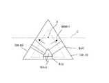
図1,図2には、種結晶として、{10−11}面を有する六角錐結晶1を用いて、III族窒化物結晶を結晶成長する場合が示されている。なお、図2は図1の断面図である。 1 and 2 show a case where a group III nitride crystal is grown using a hexagonal pyramid crystal 1 having a {10-11} plane as a seed crystal. 2 is a cross-sectional view of FIG.
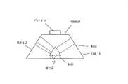
また、図3には、種結晶として、(0001)面を主面とする板状結晶2を用いて、III族窒化物結晶を結晶成長する場合が示されている。 FIG. 3 shows a case where a group III nitride crystal is grown using a plate crystal 2 having a (0001) plane as a main surface as a seed crystal.
図2,図3のいずれの場合も、成長したIII族窒化物結晶の結晶上部A,Bは、転位が伝播しにくく、転位密度が低くなっている(低転位密度となっている)。 In both cases of FIGS. 2 and 3, the crystal tops A and B of the grown group III nitride crystal are less likely to propagate dislocations and have a low dislocation density (low dislocation density).
上記したいずれかの結晶製造方法で作製されたIII族窒化物結晶が得られる。A group III nitride crystal produced by any of the above-described crystal production methods is obtained.
また、上記の結晶製造方法で作製されたIII族窒化物結晶であれば、所望とする特定の結晶面(例えば(0001)面)の貫通転位密度が少ない高品質のIII族窒化物結晶を提供することができる。Further,if the aboveSymbol of crystal manufacturing method III nitride made with crystals, a specific crystal plane (e.g. (0001) plane) of the threading dislocation density is less high-quality group III-nitride crystal to a desired Can be provided.
具体的に、種結晶として、{10−11}面を有する六角錐結晶1を用いて結晶成長したIII族窒化物結晶は、図2に示すように、結晶上部Aが低転位密度となっている。また、種結晶として、(0001)面を主面とする板状結晶2を用いて結晶成長したIII族窒化物結晶は、図3に示すように、結晶上部Bが低転位密度となっている。 Specifically, a group III nitride crystal grown using a hexagonal pyramid crystal 1 having a {10-11} plane as a seed crystal has a low dislocation density in the upper portion A of the crystal as shown in FIG. Yes. In addition, as shown in FIG. 3, a group III nitride crystal grown using a plate-like crystal 2 having a (0001) plane as a main surface as a seed crystal has a low dislocation density in the upper part B of the crystal. .
本発明は、上記により得られたIII族窒化物結晶を加工して作製した特定の結晶面(例えば(0001)面)を主面とする基板であることを特徴としている。The present invention is characterized in that it is a substrate whose principal surface is a specific crystal plane (for example, (0001) plane) produced by processing a group III nitride crystalobtained as described above .
また、この発明によれば、上記のIII族窒化物結晶を加工して作製した特定の結晶面(例えば(0001)面)を主面とする基板であるので、所望とする特定の結晶面(例えば(0001)面)の貫通転位密度が少ない高品質のIII族窒化物結晶の基板を提供することができる。Further, according to thepresent invention, since the substrate has a specific crystal plane (for example, (0001) plane) produced by processing the group II / II nitride crystal asdescribed above, the specific crystal plane desired A high-quality group III nitride crystal substrate having a low threading dislocation density (for example, (0001) plane) can be provided.
具体的に、例えば図2に示すように結晶成長したIII族窒化物結晶を、図4に示すような破線Cの部分(図4の例では、結晶の上部A付近を通る(0001)面)で切断し、これを図5に示すような特定の結晶面((0001)面)を主面とする基板(低転位密度基板)とすることができる。 Specifically, for example, a group III nitride crystal grown as shown in FIG. 2 is shown in a portion indicated by a broken line C as shown in FIG. 4 (in the example of FIG. 4, it passes through the vicinity of the upper part A of the crystal (0001) plane). This can be cut into a substrate (low dislocation density substrate) having a specific crystal plane ((0001) plane) as a main surface as shown in FIG.
本発明により得られたIII族窒化物結晶の特定の結晶面(例えば(0001)面)上、または、基板上に半導体デバイスを作製することができる。A semiconductor device can be manufactured on a specific crystal plane (for example, (0001) plane) of the group III nitride crystal obtained by the present invention or on a substrate .
上記の構成によれば、III族窒化物結晶の特定の結晶面(例えば(0001)面)上、または、基板上に作製された半導体デバイスであるので、高性能,高信頼性の半導体デバイスを提供することができる。According to the above configuration, since the semiconductor device is manufactured ona specific crystal plane (for example, (0001) plane) of a group III nitride crystal or on a substrate, a high-performance and high-reliability semiconductor device can be obtained. Can be provided.
図6には、図4のIII族窒化物結晶を破線Cの部分で切断,研磨して形成した低転位密度の(0001)面基板(図5の基板)上に作製したデバイスの一例が示されている。このデバイスは、低転位密度の(0001)面基板(図5の基板)上に作製されているので、高性能,高信頼性のものとなる。 FIG. 6 shows an example of a device fabricated on a low dislocation density (0001) plane substrate (substrate of FIG. 5) formed by cutting and polishing the group III nitride crystal of FIG. Has been. Since this device is fabricated on a (0001) plane substrate (substrate in FIG. 5) having a low dislocation density, it has high performance and high reliability.
実施例1では、アルカリ金属としてNa(ナトリウム)を用い、III族金属原料としてGa(ガリウム)を用い、窒素原料として窒素ガスを使用し、(0001)面を主面とするGaN種結晶に、III族窒化物としてGaNを結晶成長させた。なお、ここで、Na,Gaはあらかじめ混合融液として融液保持容器中に保持し、窒素を気相から融液中に溶解してGaNを結晶成長させた。 In Example 1, Na (sodium) is used as an alkali metal, Ga (gallium) is used as a Group III metal raw material, nitrogen gas is used as a nitrogen raw material, and a GaN seed crystal having a (0001) plane as a main surface, GaN was grown as a group III nitride. Here, Na and Ga were previously held in a melt holding container as a mixed melt, and nitrogen was dissolved from the gas phase into the melt to grow GaN crystals.
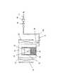
図7は実施例1に用いられる結晶製造装置の構成例を示す図である。FIG. 7 is a diagram illustrating a configuration example of the crystalmanufacturing apparatus used in the first embodiment.
図7の結晶製造装置は、ステンレス製の閉じた形状の反応容器11内に、アルカリ金属とIII族金属を含む融液22を保持し、結晶成長を行なうための融液保持容器12が設けられている。The crystalmanufacturing apparatus of FIG. 7 is provided with a
この融液保持容器12は反応容器11から取り外すことができる。また、融液保持容器12の材質はBNである。 The
また、反応容器11の内部空間19に窒素原料となる窒素(N2)ガスを充満させ、かつ反応容器11内の窒素(N2)圧力を調整することを可能にするガス供給管14が反応容器11を貫通して装着されている。Also, nitrogen (N2) as a nitrogen source in the
窒素ガスの圧力は圧力制御装置16で調整する事ができる。 The pressure of the nitrogen gas can be adjusted by the
また、反応容器11内の全圧力は圧力計18でモニターされる。 The total pressure in the
また、反応容器11の外側にはヒーター13が設置されている。 A
また、反応容器11は、バルブ21の部分で結晶成長装置から取り外すことが可能であり、反応容器11の部分のみをグローブボックスに入れて作業することができる。 The
以下に、図7の結晶製造装置を使用した実施例1でのGaNの結晶成長方法を説明する。Below, the crystal growth method of GaN in Example 1 using the crystalmanufacturing apparatus of FIG. 7 is demonstrated.
まず、反応容器11をバルブ21の部分で結晶成長装置から分離し、Ar雰囲気のグローブボックスに入れる。 First, the
次いで、BN製の融液保持容器12に、(0001)面を主面とするGaN種結晶24とガリウム(Ga)とナトリウム(Na)を入れる。 Next, a
次いで、融液保持容器12を融液保持容器保持台20に置き、反応容器11内に設置する。 Next, the
次いで、反応容器11を密閉し、バルブ21を閉じ、反応容器11内部を外部雰囲気と遮断する。 Next, the
次いで、反応容器11をグローブボックスから出し、結晶成長装置に組み込む。 Next, the
すなわち、反応容器11をヒーター13がある所定の位置に設置し、バルブ21の部分で窒素のガス供給ライン14に接続する。 That is, the
次いで、バルブ15,21を開け、反応容器11内に窒素ガスを入れる。このとき、圧力制御装置16で窒素圧力を1MPaにした。この圧力は、実施例1で使用した装置において、結晶成長温度(775℃)に昇温したときに、反応容器11内の全圧が1.5MPaになる圧力である。 Next, the
次いで、バルブ15とバルブ21を閉じる。これにより、反応容器11は密閉される。 Next, the
次いで、ヒーター13に通電し、融液22を室温(27℃)から結晶成長温度まで1時間で昇温する。結晶成長温度は775℃とした。 Next, the
昇温に追随して密閉された反応容器11内の圧力は上昇し、結晶成長温度775℃に達した時の反応容器11内の全圧は1.5MPaになった。 The pressure in the sealed
この状態で500時間保持した後、室温まで降温する。 After holding in this state for 500 hours, the temperature is lowered to room temperature.
結晶成長終了後、反応容器11を開けると、種結晶24上に{10−11}面で形成された六角錐状のGaN23が成長していた。When the
成長したGaN結晶23は、結晶上部の欠陥密度がエッチピット密度評価で106cm−2以下であった。
本発明は、光ディスク用青紫色光源、紫外光源(全面)、電子写真用青紫色光源、III族窒化物電子デバイスなどに利用可能である。 The present invention can be used for a blue-violet light source for optical disks, an ultraviolet light source (entire surface), a blue-violet light source for electrophotography, a group III nitride electronic device, and the like.
1,2 種結晶
11 反応容器
12 融液保持容器
13 ヒーター
14 ガス供給管
15,21 バルブ
16 圧力制御装置
18 圧力計
23 GaN
24 種結晶
1, 2
24 seed crystals
Claims (3)
Translated fromJapanese少なくともアルカリ金属とIII族金属と窒素が溶解した融液からIII族窒化物結晶を成長させる際に種結晶に対して、基板の主面とはならない{10−11}面を成長面として形成しながらIII族窒化物結晶を成長する工程と、
前記III族窒化物結晶のうち前記種結晶よりも低転位密度である部分を加工して特定の結晶面を前記主面とする基板を作製する工程とを含むことを特徴とするIII族窒化物の結晶の基板の製造方法。A method for producing a group III nitride crystal substrate, comprising:
When a group III nitride crystal is grown from a melt in which at least an alkali metal, a group III metal, and nitrogen are dissolved, a {10-11} plane thatis not the main surface of the substrate is formed as a growthsurface with respect to the seed crystal. While growing a group III nitride crystal,
III-nitride, which comprises a step of preparing a substrate for said group IIIsaid major surface a specific crystal plane be processed portions that are low dislocation density than the seed crystal of the nitride crystal Method for manufacturing a crystal substrate.
Priority Applications (1)
| Application Number | Priority Date | Filing Date | Title |
|---|---|---|---|
| JP2004059231AJP4560310B2 (en) | 2004-03-03 | 2004-03-03 | Method for manufacturing substrate of group III nitride crystal |
Applications Claiming Priority (1)
| Application Number | Priority Date | Filing Date | Title |
|---|---|---|---|
| JP2004059231AJP4560310B2 (en) | 2004-03-03 | 2004-03-03 | Method for manufacturing substrate of group III nitride crystal |
Publications (2)
| Publication Number | Publication Date |
|---|---|
| JP2005247625A JP2005247625A (en) | 2005-09-15 |
| JP4560310B2true JP4560310B2 (en) | 2010-10-13 |
Family
ID=35028482
Family Applications (1)
| Application Number | Title | Priority Date | Filing Date |
|---|---|---|---|
| JP2004059231AExpired - Fee RelatedJP4560310B2 (en) | 2004-03-03 | 2004-03-03 | Method for manufacturing substrate of group III nitride crystal |
Country Status (1)
| Country | Link |
|---|---|
| JP (1) | JP4560310B2 (en) |
Families Citing this family (9)
| Publication number | Priority date | Publication date | Assignee | Title |
|---|---|---|---|---|
| JP4856934B2 (en) | 2005-11-21 | 2012-01-18 | 株式会社リコー | GaN crystal |
| TWI490918B (en)* | 2006-01-20 | 2015-07-01 | Univ California | Improved growth method for semi-polar nitriding (aluminum, indium, gallium, boron) |
| US8545626B2 (en) | 2008-03-03 | 2013-10-01 | Mitsubishi Chemical Corporation | Nitride semiconductor crystal and its production method |
| JP5328682B2 (en) | 2010-01-13 | 2013-10-30 | 日立電線株式会社 | Method for producing group III nitride crystal and method for producing group III nitride semiconductor substrate |
| JP5699493B2 (en)* | 2010-08-31 | 2015-04-08 | 株式会社リコー | Method for producing group III nitride single crystal |
| JP5328999B2 (en)* | 2013-02-22 | 2013-10-30 | 日立電線株式会社 | Method for manufacturing group III nitride semiconductor substrate |
| JP6186763B2 (en)* | 2013-03-08 | 2017-08-30 | 株式会社リコー | Method for producing group 13 nitride crystal, method for producing group 13 nitride crystal substrate, and group 13 nitride crystal substrate |
| JP6398213B2 (en)* | 2014-02-13 | 2018-10-03 | 株式会社リコー | Method for producing group 13 nitride crystal |
| JP6337526B2 (en)* | 2014-03-10 | 2018-06-06 | 株式会社リコー | Method for producing group 13 nitride crystal |
Family Cites Families (2)
| Publication number | Priority date | Publication date | Assignee | Title |
|---|---|---|---|---|
| JP4278330B2 (en)* | 2002-01-10 | 2009-06-10 | 株式会社リコー | Group III nitride crystal production method and group III nitride crystal production apparatus |
| JP4801315B2 (en)* | 2002-01-29 | 2011-10-26 | 株式会社リコー | Method for producing group III nitride crystal |
- 2004
- 2004-03-03JPJP2004059231Apatent/JP4560310B2/ennot_activeExpired - Fee Related
Also Published As
| Publication number | Publication date |
|---|---|
| JP2005247625A (en) | 2005-09-15 |
Similar Documents
| Publication | Publication Date | Title |
|---|---|---|
| CN107407008B (en) | Method for manufacturing group III nitride semiconductor crystal substrate | |
| US9096950B2 (en) | Nitride crystal and method for producing the same | |
| US9670594B2 (en) | Group III nitride crystals, their fabrication method, and method of fabricating bulk group III nitride crystals in supercritical ammonia | |
| JP4560310B2 (en) | Method for manufacturing substrate of group III nitride crystal | |
| KR20190133274A (en) | Iii-n single crystals | |
| US9790617B2 (en) | Group III nitride bulk crystals and their fabrication method | |
| CN107002278B (en) | Group III nitride crystal, method of making the same, and method of making bulk Group III nitride crystal in supercritical ammonia gas | |
| JP4278330B2 (en) | Group III nitride crystal production method and group III nitride crystal production apparatus | |
| JP2006290677A (en) | Nitride-based compound semiconductor crystal manufacturing method and nitride-based compound semiconductor substrate manufacturing method | |
| JP2012051746A (en) | Method for producing group iii nitride single crystal | |
| WO2019017043A1 (en) | Single-crystal aln production method and single-crystal aln | |
| JP2018043893A (en) | Method for producing group 13 nitride crystal and method for producing group 13 nitride crystal substrate | |
| JP4271408B2 (en) | Group III nitride crystal production method | |
| WO2010084681A1 (en) | Group iiib nitride crystal manufacturing method | |
| JP2011046548A (en) | Template, method for producing the template, crystal grown using the template, and method and apparatus for producing the crystal | |
| JP2003095790A (en) | Method of preparing seed crystal of zinc oxide and method of growing single crystal of zinc oxide | |
| JP5883912B2 (en) | Nitride crystal and method for producing the same | |
| EP3146093A1 (en) | Group iii nitride bulk crystals and their fabrication method | |
| JP2018016497A (en) | Method for manufacturing group iii nitride semiconductor | |
| JP4640943B2 (en) | Group III nitride crystal manufacturing method | |
| JP2024003681A (en) | How to reuse SAM board | |
| JP2016172692A (en) | Nitride crystal and method for producing the same | |
| JP2005015316A (en) | How to grow artificial quartz | |
| JP2015078121A (en) | Nitride crystal and method for producing the same | |
| JPH05221772A (en) | Apparatus and method for producing compound semiconductor single crystal |
Legal Events
| Date | Code | Title | Description |
|---|---|---|---|
| RD02 | Notification of acceptance of power of attorney | Free format text:JAPANESE INTERMEDIATE CODE: A7422 Effective date:20060201 | |
| RD04 | Notification of resignation of power of attorney | Free format text:JAPANESE INTERMEDIATE CODE: A7424 Effective date:20060210 | |
| A621 | Written request for application examination | Free format text:JAPANESE INTERMEDIATE CODE: A621 Effective date:20060627 | |
| A977 | Report on retrieval | Free format text:JAPANESE INTERMEDIATE CODE: A971007 Effective date:20081117 | |
| A131 | Notification of reasons for refusal | Free format text:JAPANESE INTERMEDIATE CODE: A131 Effective date:20081125 | |
| A521 | Request for written amendment filed | Free format text:JAPANESE INTERMEDIATE CODE: A523 Effective date:20090123 | |
| RD02 | Notification of acceptance of power of attorney | Free format text:JAPANESE INTERMEDIATE CODE: A7422 Effective date:20090730 | |
| RD05 | Notification of revocation of power of attorney | Free format text:JAPANESE INTERMEDIATE CODE: A7425 Effective date:20090909 | |
| A131 | Notification of reasons for refusal | Free format text:JAPANESE INTERMEDIATE CODE: A131 Effective date:20091222 | |
| A521 | Request for written amendment filed | Free format text:JAPANESE INTERMEDIATE CODE: A523 Effective date:20100218 | |
| TRDD | Decision of grant or rejection written | ||
| A01 | Written decision to grant a patent or to grant a registration (utility model) | Free format text:JAPANESE INTERMEDIATE CODE: A01 Effective date:20100720 | |
| A01 | Written decision to grant a patent or to grant a registration (utility model) | Free format text:JAPANESE INTERMEDIATE CODE: A01 | |
| A61 | First payment of annual fees (during grant procedure) | Free format text:JAPANESE INTERMEDIATE CODE: A61 Effective date:20100726 | |
| R150 | Certificate of patent or registration of utility model | Ref document number:4560310 Country of ref document:JP Free format text:JAPANESE INTERMEDIATE CODE: R150 Free format text:JAPANESE INTERMEDIATE CODE: R150 | |
| FPAY | Renewal fee payment (event date is renewal date of database) | Free format text:PAYMENT UNTIL: 20130730 Year of fee payment:3 | |
| LAPS | Cancellation because of no payment of annual fees |