JP4556282B2 - Organic EL device and method for manufacturing the same - Google Patents
Organic EL device and method for manufacturing the sameDownload PDFInfo
- Publication number
- JP4556282B2 JP4556282B2JP2000101304AJP2000101304AJP4556282B2JP 4556282 B2JP4556282 B2JP 4556282B2JP 2000101304 AJP2000101304 AJP 2000101304AJP 2000101304 AJP2000101304 AJP 2000101304AJP 4556282 B2JP4556282 B2JP 4556282B2
- Authority
- JP
- Japan
- Prior art keywords
- layer
- protective layer
- film
- organic
- gas
- Prior art date
- Legal status (The legal status is an assumption and is not a legal conclusion. Google has not performed a legal analysis and makes no representation as to the accuracy of the status listed.)
- Expired - Fee Related
Links
Images


Classifications
- H—ELECTRICITY
- H10—SEMICONDUCTOR DEVICES; ELECTRIC SOLID-STATE DEVICES NOT OTHERWISE PROVIDED FOR
- H10K—ORGANIC ELECTRIC SOLID-STATE DEVICES
- H10K59/00—Integrated devices, or assemblies of multiple devices, comprising at least one organic light-emitting element covered by group H10K50/00
- H10K59/80—Constructional details
- H10K59/87—Passivation; Containers; Encapsulations
- H10K59/873—Encapsulations
- H—ELECTRICITY
- H10—SEMICONDUCTOR DEVICES; ELECTRIC SOLID-STATE DEVICES NOT OTHERWISE PROVIDED FOR
- H10K—ORGANIC ELECTRIC SOLID-STATE DEVICES
- H10K50/00—Organic light-emitting devices
- H10K50/80—Constructional details
- H10K50/84—Passivation; Containers; Encapsulations
- H10K50/844—Encapsulations
- H10K50/8445—Encapsulations multilayered coatings having a repetitive structure, e.g. having multiple organic-inorganic bilayers
- Y—GENERAL TAGGING OF NEW TECHNOLOGICAL DEVELOPMENTS; GENERAL TAGGING OF CROSS-SECTIONAL TECHNOLOGIES SPANNING OVER SEVERAL SECTIONS OF THE IPC; TECHNICAL SUBJECTS COVERED BY FORMER USPC CROSS-REFERENCE ART COLLECTIONS [XRACs] AND DIGESTS
- Y10—TECHNICAL SUBJECTS COVERED BY FORMER USPC
- Y10T—TECHNICAL SUBJECTS COVERED BY FORMER US CLASSIFICATION
- Y10T428/00—Stock material or miscellaneous articles
- Y10T428/24—Structurally defined web or sheet [e.g., overall dimension, etc.]
- Y10T428/24942—Structurally defined web or sheet [e.g., overall dimension, etc.] including components having same physical characteristic in differing degree
Landscapes
- Physics & Mathematics (AREA)
- Optics & Photonics (AREA)
- Chemical & Material Sciences (AREA)
- Inorganic Chemistry (AREA)
- Electroluminescent Light Sources (AREA)
Description
Translated fromJapanese【0001】
【発明の属する技術分野】
本発明は、基板上に、互いに対向する一対の電極間に有機発光材料を配置した構造体を備え、該構造体の外表面に有機発光材料を被覆する保護層を有する有機EL(エレクトロルミネッセンス)素子およびその製造方法に関する。
【0002】
【従来の技術】
一般的に、有機EL素子は、基板上に、互いに対向する一対の電極間に有機発光材料を配置した構造体を備える。しかし、使用雰囲気中の水分により有機発光材料が劣化し、構造体における本来の発光領域に無発光領域が形成され、表示品位の悪化を招く。この問題に対して、特開平7−161474号公報では、CVD法(化学気相成長法)により成膜された炭素または珪素からなる無機アモルファス性膜を、構造体の外表面に有機発光材料を被覆するように形成し、これを保護膜として用いることが提案されている。
【0003】
【発明が解決しようとする課題】
しかしながら、上記従来公報について行った本発明者等の検討によれば、従来の保護膜は構造体に対する被覆性が不十分であるために、水分に対する抵抗性が低く、高温高湿(例えば、65℃、95%RH)雰囲気で動作させたところ、無発光領域が発生してしまうことがわかった。
【0004】
そこで、本発明は上記問題に鑑み、基板上に、互いに対向する一対の電極間に有機発光材料を配置した構造体を備え、該構造体の外表面に有機発光材料を被覆する保護層を有する有機EL素子において、保護層の構造体に対する被覆性を向上させることを目的とする。
【0005】
【課題を解決するための手段】
上記目的を達成するため、請求項1〜請求項14記載の発明では、基板(1)上に、互いに対向する一対の電極(2、5)間に有機発光材料(3、4)を配置した構造体を備える有機EL素子であって、該構造体の外表面に、該有機発光材料を被覆する保護層(6)を有し、この保護層が原子層成長法により形成されており、該保護層の全応力は−150MPa〜150MPaであり、該保護層は、該保護層に発生する応力を緩和するための応力緩和成分としての窒素を含有しているものであるか、または、異なる膜質の層が積層されてなるものであることを特徴としている。
【0006】
原子層成長法(以下、本欄にてALE法という)は、被形成体の表面で反応するのを利用するため、被形成体の表面形状に沿って均一な膜を形成できる。そのため、ALE法により形成された保護層は、従来のCVD法等により形成される膜と比べて、構造体に対する被覆性が良好なものとなる。よって、本発明によれば、保護層の構造体に対する被覆性を向上させることができる。また、保護層の構造体に対する被覆性が向上すれば、水分に対する抵抗性も良好とできるため、水分により構造体に無発光領域が形成されるのを防止することができる。また、保護層を該保護層に発生する応力を緩和するための応力緩和成分を含有するものとすれば、保護層に発生する応力を緩和し、保護層に亀裂等の損傷が発生するのを回避できる。
【0007】
また、請求項2の発明では、請求項1記載の保護層(6)の上に、該保護層を保護する樹脂膜(7)を形成したことを特徴としており、該樹脂膜により保護層が保護されるため、保護層を薄くしても水分に対する抵抗性を確保できる。そして、保護層を薄くできるということは、ALE法による保護層の成膜時間を短縮でき、スループットを向上させることができる。
【0008】
また、請求項3の発明では、請求項1または2記載のALE法を、有機発光材料(3、4)のガラス転移点以下の成膜温度にて行うことを特徴としている。保護層の成膜時の温度が、有機発光材料のガラス転移点よりも大きいと、保護層の成膜中に、下地である構造体中の有機発光材料が結晶化して発光効率が低下してしまう可能性があるが、本発明によれば、そのような問題を回避でき、より発光効率の高い有機EL素子を提供することができる。
【0009】
また、請求項4の発明では、保護層(6)を、互いに内部に発生する応力の異なる層を積層してなるものとしたことを特徴としている。通常、ALE法により形成された保護層は、成膜時に体積収縮を起こすため、保護層自体が縮むような応力が発生し保護層に亀裂等が発生する可能性がある。その点、本発明によれば、保護層が、互いに内部に発生する応力の異なる層よりなるため、保護層を、比較的応力が低く応力を緩和する膜(応力緩和膜)と比較的応力が高く応力を緩和しにくい膜(非応力緩和膜)とにより、形成されたものとすることができる。
【0010】
そして、応力緩和膜によって応力を緩和することができる。また、応力緩和膜は、通常、内部欠陥等の多い膜となるので構造体に対する被覆性が不十分となりやすいが、この点については、内部欠陥の少ない非応力緩和膜の方にて、被覆性を確保できるので大丈夫である。よって、保護層に発生する応力を緩和して亀裂等の損傷の可能性を低減した保護層を実現することができ、請求項1〜請求項3の発明の効果を、より高レベルにて実現できる。
【0011】
ここで、互いに内部に発生する応力の異なる層は、互いにALE法における成膜条件を異ならせることにより形成したものとすることができる(請求項5の発明)。成膜条件(成膜温度等)を異ならせることにより膜質を変えることができるため、互いに応力の異なる応力緩和膜と非応力緩和膜とを形成することができる。なお、応力緩和膜と非応力緩和膜とは同一材料でも異種材料でも構わない。
【0013】
ここで、請求項1記載の保護層としては、請求項6の発明のように、応力緩和成分を含有する層と応力緩和成分を含有しない層とを積層した積層構造でも良い。それによれば、応力緩和成分を含有する層が上記応力緩和膜として機能し、応力緩和成分を含有しない層が上記非応力緩和膜として機能するため、請求項4の発明と同様の効果が得られる。
【0014】
また、請求項6の発明における応力緩和成分を含有する層は、請求項7の発明のように、ALE法による成膜時に、保護層(6)を構成する材料ガスとともに、該材料ガスとは異なり応力緩和成分として作用する元素成分を含むガスを使用することにより、形成されたものとできる。具体的には、応力緩和成分として作用する元素成分として窒素元素を含む窒素化合物のガスを用いることができる。
【0015】
また、保護層に発生する応力を緩和して亀裂等の損傷の可能性を低減した保護層を実現するにあたっては、請求項9の発明のように、保護層(6)を、ALE法により形成された層(6a)と、ALE法とは異なる方法(以下、非ALE法という)により形成された層(6b)との組合せから構成したものとしても良い。
【0016】
それによっても、互いの層の膜質を変えることができ、ALE法により形成された層を上記応力緩和膜、非ALE法により形成された層を上記非応力緩和膜として機能させることができるため、請求項4の発明と同様の効果を実現することができる。さらに、請求項9の発明の効果としては、保護層の一部を非ALE法により形成するため、保護層の全部を比較的成膜時間の長いALE法にて成膜する場合に比べて、成膜時間を短くすることも可能である。
【0017】
ここで、ALE法により形成された層(ALE層)と、非ALE法により形成された層(非ALE層)との組合せとしては、請求項10の発明のように、非ALE層(6b)を構造体(2〜5)の直上に形成し、その上にALE層(6a)を形成した構成としても良いし、その逆、即ち、請求項11の発明のように、ALE層(6a)を構造体(2〜5)の直上に形成し、その上に非ALE層(6b)を形成した構成としても良い。また、上記請求項5に記載の有機EL素子において、原子層成長法における成膜条件は、成膜温度やパージに用いるガス種類とすることができる。
【0018】
また、請求項16に記載の発明は、構造体の外表面に原子層成長法を用いて有機発光材料を被覆する保護層(6)を形成する工程を備える有機EL素子の製造方法であって、当該原子層成長法による保護層の形成工程では、前記構造体が形成されたガラス基板(1)を、反応炉に入れて、その反応炉を真空にし、
有機金属成分を含む第1のガスと酸素を含む第2のガスとを前記反応炉に交互に導入しながら、前記反応炉内の前記ガラス基板の温度を、前記有機発光材料のガラス転移点以下である第1の温度となるように制御することにより、前記第1のガスおよび前記第2のガスにより前記保護層の第1の層を形成し、この第1の層の形成後、前記反応炉内の前記ガラス基板の温度を、前記第1の温度とは異なる温度であって且つ前記有機発光材料のガラス転移点以下である第2の温度となるように制御することにより、前記第1のガスおよび前記第2のガスにより前記保護層の第2の層を形成するものであり、
この第1および第2のガスを交互に導入することを複数サイクル繰り返し行うことによって、前記有機金属成分を含む金属酸化物としての所望厚さを有する前記保護層を形成するものであり、前記第1のガスはトリメチルアルミニウムよりなり、前記第2のガスは気化したH2Oよりなり、
前記ガラス基板における前記第2の温度を前記第1の温度よりも高いものとすることにより、前記第1の層を応力緩和膜としてのアルミナ膜とし、前記第2の層を非応力緩和膜としてのアルミナ膜とすることを特徴とする。なお、上記各手段の括弧内の符号は、後述する実施形態に記載の具体的手段との対応関係を示す一例である。
【0019】
【発明の実施の形態】
以下、本発明を図に示す実施形態について説明する。なお、以下の各実施形態において、互いに同一部分には、各図中、同一符号を付してある。
【0020】
(第1実施形態)
図1は、本発明の第1実施形態に係る有機EL(エレクトロルミネッセンス)素子100の部分断面図であり、図2は図1中の矢印A方向から視た有機EL素子100の全体概略平面図である。なお、図1は図2中のB−B断面に沿った部分断面図である。
【0021】
1はガラス基板であり、このガラス基板1の平坦な一面上には、ITO(インジウムチンオキサイド)膜等の透明導電膜よりなり、ホール注入電極として機能する陽極(下部電極)2が形成されている。図2に示す様に、陽極2は、基板1上にスパッタ法により成膜されたITO膜(例えば厚さ150nm)をエッチング等にてパターニングすることにより、x方向に延びるストライプ状に形成されたものであり、例えば、500μm幅の帯状のものが、50μmの間隔でストライプ状に並んだものとしている。
【0022】
この陽極2上には、本発明でいう有機発光材料としてのホール輸送層3及び有機発光層4が、順次形成されている。本例では、ホール輸送層3として、ガラス転移点(以下、Tg点という)が約130℃のテトラトリフェニルアミン(以下、TPTEという)を約40nmの膜厚で、有機発光層4として、Tg点が170℃のトリス(8−キノリノール)アルミニウム(以下、Alqという)に対して蛍光物質のキナクリドン化合物(Tg点存在せず)をドープしたものを約50nmの膜厚で、約10-6Torrの真空度で順次蒸着している。
【0023】
そして、有機発光層4の上には、金属等よりなり、電子注入電極として機能する陰極(上部電極)5が形成されている。本例では、陰極5は、マスクを用いた真空蒸着によって形成されたAl(アルミニウム)膜(例えば厚さ100nm)であり、図2に示す様に、陽極2と略直交するようにy方向へ延びるストライプ形状をなす。例えば、陰極5は、500μm幅の帯状のものが、50μmの間隔でストライプ状に並んだものとしている。
【0024】
このように、本有機EL素子100は、陽極2と陰極5とが交差して重なり合う領域が、発光表示を行うべき部分である表示画素(本来の発光領域)を構成しているドットマトリクスディスプレイである。図2では、陽極2と陰極5とが重なり合って、複数個の矩形状の表示画素Gを構成している。
【0025】
このように、本有機EL素子100は、基板1上に、互いに対向する一対の電極2、5間に有機発光材料4を配置してなる構造体2〜5を備えるが、さらに、この構造体2〜5の外表面に、有機発光材料3、4を被覆して外部環境から保護する保護層6を有する。本例では、保護層6は原子層成長法(アトミックレイヤーエピタキシー法、以下、ALE法という)により、約400nmの厚さで形成されたアルミナ(Al2O3)膜である。
【0026】
保護層6は、陰極5の上部及び陰極5が形成されていない有機発光層4の上部において、図2に示す様に(便宜上、保護層6にハッチングを施してあるが断面ではない)、有機発光層4の成膜領域(二点鎖線にて図示)よりも広い範囲を被覆しており、下地である有機発光層4を保護している。また、石英ガラス製のマスク等を用いて成膜することにより、保護層6の成膜領域は、図2に示す様に、陽極2と陰極5における外部回路(図示せず)との接続端子部2a、5aが露出されるように設定されている。
【0027】
かかる有機EL素子100においては、上記外部回路によって陽極2と陰極5との間に所定のデューティ比を有する駆動用の直流電圧を印加することにより、所望の表示画素Gにおいて、陽極2から正孔、陰極5から電子がそれぞれ移動してきて、これら正孔及び電子が有機発光層4内で再結合し、その放出エネルギーで蛍光材料(本例ではキナクリドン化合物)が発光するようになっている。この発光はガラス基板1側から取り出される。
【0028】
ところで、本実施形態では、構造体2〜5を保護する保護層6において、従来の有機EL素子では行われていなかったALE法を用いて形成した独自の構成を採用している。次に、この保護層6の形成方法や構成等について、より詳細に述べる。まず、保護層6の形成方法の一具体例を図3に示す工程の流れ図を参照して述べる。
【0029】
まず、陽極2、各有機層3、4、陰極5が成膜されたガラス基板(有機EL薄膜付きガラス基板)1上に石英ガラス製のマスクをホルダを用いて固定し、反応炉に入れた。その反応炉を40Pa程度の真空にし、N2ガスを400sccm程度流しながら、該ガラス基板1を加熱し、基板温度を100℃に安定させた。
【0030】
その後、TMA(トリメチルアルミニウム)を原料ボトル内にて28℃、H2Oを原料ボトル内にて室温(24℃)に保持し、減圧下で気化させ、次のようにして、キャリアガスであるN2ガス(流量は400sccm)により、反応炉へ交互に導入した。まず、気化TMAを0.6秒導入した後、基板表面に吸着した分子以外の気相に存在する過剰のTMAを取り除くため、パージガスとしてN2ガスを2.4秒導入した。その後、同様に気化H2Oを1.0秒、N2パージガスを4.0秒のガス導入時間(パルス時間)にて成膜した。
【0031】
このTMA導入→パージ→H2O導入→パージのサイクルを5000回繰り返し(約11時間)、成膜を行った。この間、反応炉の圧力は150〜300Paであり、基板温度は反応炉内のヒータによって100℃に保持した。成膜が終了した後は、N2ガスを400sccm導入しながら、放置冷却を行い、基板温度が70℃になった時点で反応炉を大気圧にし、基板1を取り出した。これにより、保護層6として、膜厚約400nmのアルミナ(Al2O3)が得られた。なお、膜厚は保護層6の断面をTEM(電子透過型顕微鏡)観察することで求めた。
【0032】
ここで、ALE法による保護層6の成膜時の基板温度(成膜温度)については、予め成膜されている有機発光材料3、4(本例ではTPTE、Alq)のTg点以下の温度とすることが好ましい。これは、該成膜温度が該Tg点よりも高いと有機発光材料の結晶化が進み、発光効率が低下するためである。上記具体例では、有機発光材料3、4に使用されている材料の中で最も低いTPTEのTg点130℃よりも約30℃低い100℃に、基板温度を設定した。
【0033】
図4は、成膜温度(基板温度)により、素子の電圧−輝度特性がどのように変化するかを確認した結果を示すグラフである。成膜温度が100℃で成膜した時と130℃(TPTEのTg点)で成膜した時とでは、ほとんど差は認められなかったが、150℃で成膜した時は、明らかに電圧−輝度特性が右側にシフトしていることがわかる。これは、成膜温度が150℃で保護層6を形成する工程中に、TPTEの結晶化が進み、発光効率が低下したためと考えられる。
【0034】
次に、保護層6の膜厚、組成、加工、及びALE法における成膜装置等について、留意点を述べる。
【0035】
[保護層の膜厚]本実施形態では、保護層6の膜厚は問わず、保護層6としての要求特性が満足できればよい。一般的に膜厚は厚い方が信頼性は高くなるが、ALE法による成膜の場合は成膜時間が長いため、プロセスと保護特性の許容範囲であれば薄くてもよい。ただし、プロセスにおいて下地(構造体2〜5)に発生する異物を被覆してピンホールの発生等を防止するために、経験的には、少なくとも5nm以上の膜厚が望ましい。更に言えば50nm以上が望ましい。
【0036】
また、ALE法においては、ステップカバレッジ率は、ガスの基板吸着率が一様ならば、ほぼ100%であるため、基板表面上さえ清浄であれば、たとえ薄くともピンホールや欠陥が発生すること無く、大気中の水分や酸素などから有機発光材料3、4を十分に保護できる。保護層6を薄膜化することにより、保護層6の全応力を小さく出来るので、クラック等の発生を回避することが可能となる。
【0037】
また、基板加工時のスクラッチ(ひっかき傷)や、製品レベルでの組み付け時における物理的ダメージから保護するには、ALE法で保護層6を成膜した後、この物理的ダメージから保護層6を保護する樹脂膜(物理的ダメージ保護層)を、保護層6の上部に設ければ良い。図5は、上記有機EL素子100において、樹脂膜7を設けた構成を示す部分的な概略断面図である。
【0038】
ここで、樹脂膜7の組成、成膜法、厚さは問わない。例えば、保護層6として、ALE法で上記図3に準じてAl2O3を50nm程度成膜し、その後、樹脂膜7として、蒸着法などでパラキシレン重合体などを約2μm成膜すればよい。その他、樹脂膜7としては、スピンコート法、スクリーン印刷法、塗布法などによって形成されるゴム系材料、アクリル系樹脂、シリコーン、エポキシ系樹脂などの有機系材料の膜でも良い。なお、樹脂膜7の成膜過程(スピンコート法での硬化処理等を含む)であってもやはり有機発光材料3、4のTg点以下であることが望ましい。
【0039】
[保護層の組成]保護層6は、ALE法によって成膜可能であることが必要なことは勿論であるが、上述のように有機発光材料3、4のTg点以下で成膜でき、かつ、物理的・化学的に安定であって、保護層6としての要求特性を満足できれば、その組成は問わない。例えば、金属や珪素の酸化物、窒化物、酸窒化物が好ましい。
【0040】
また、保護層6を得るための原料も問わないが、原料を選択するにあたっては、一旦気化した原料ガスが再凝集したり再凝固しないように、原料の気化温度が反応炉温度及び基板温度よりも低いことが望ましい。更に言えば、原料気化温度は所望のガス濃度や圧力から決めるので、各原料の飽和蒸気圧曲線を参考にし、成膜温度よりも低い温度で気化し且つ成膜可能なガス量を得ることのできる原料が望ましい。
【0041】
例えば、アルミニウム酸化物の保護層6を得るためには、TMAやTEA(トリエチルアルミニウム)、DMAH(ジメチルアルミニウム水素化物)等のアルキル系金属と、H2O、H2O2やO2、O3、またはCH3OH、C2H5OH等のアルコール類との反応で成膜可能である。また、上記アルキル系金属とNH3等の窒素化合物ガスとを導入し互いに反応させることにより、AlN、AlxOyNzなどの窒素化合物よりなる保護層6を成膜することも可能である。また、珪素系材料としてSiCl4を用い、この気化ガスとH2Oの気化ガスとの反応からSiO2を成膜することも可能である。
【0042】
また、ALE法において、基板上からUV(紫外線)照射を行い、化学反応をより活性化させることにより、反応効率を向上させれば、有機材料3、4のTg点以下のより低温で成膜することができる。この場合、UV照射により、有機材料3、4の劣化が懸念されるが、その発光領域は陰極5にてマスクされるため、UV照射の影響は少ない。
【0043】
また、有機発光層4上に成膜する場合、保護層6の成膜における化学的反応により有機発光層4を劣化させることもありうるので注意を要する。例えばアルミニウム酸化物の保護層6をALE法で成膜する場合、TMAはルイス酸であり、成膜中の暴露時間によっては有機発光層4の露出部分を、分解等により劣化させる可能性がある。さらに、H2Oもその程度を超えれば、非発光領域の発生や増加等の劣化につながる可能性もある。
【0044】
例えば、上記図1に示す有機EL素子100のように、有機発光層4が保護層6の下地として表面に露出している場合、ALE成膜時に、有機発光層4がTMAやH2Oに直接曝されることになるので、その場合、TMAやH2Oのパルス時間や濃度に注意する。また、この場合、予め有機発光層4上に、有機発光層4に影響を与えないようなガスでALE法やその他の手法(蒸着やスパッタ等)にて劣化保護膜を成膜しておいても差し支えない。
【0045】
[保護膜の加工]有機EL素子100の陰極(上部電極)5及び陽極(下部電極)2の接続端子部(電極取り出し部)2a、5aの形成は、上述のように、石英ガラスなどのマスクなどにより保護層6が成膜されないようにするか、後の工程で除去すればよい。この接続端子部2a、5aは、後工程ではんだ付けなどの方法で配線と接合される部分である。
【0046】
ここで、上記マスクは、石英ガラスでなくとも端子部2a、5aに保護層6を成膜させないという目的を達成できればよいので、材質は問わないが、熱変形によりマスク浮きが発生してしまう問題は解決しておかなければならない。例えば厚み0.2mm程度のSUS(ステンレス)製マスクでもよいがマスク浮きに注意を払う必要がある。
【0047】
この場合は、マスクと基板が密着するよう外部から圧力を加えたり、マスク端部に逆テーパ加工などの処置を施し、ガスを回り込みにくくしておくなどの処置が好ましい。また、マスク材料の耐熱性が基板温度に対して許す限り、ゴム系材料やエポキシ樹脂などの有機系材料を用いて、塗布法、スクリーン印刷法、スピンコート法などにより、マスクを形成してもよい。
【0048】
また、マスク等を用いなくとも構造体2〜5が形成されたガラス基板1の全面に保護層6を形成し、後でフォトリソグラフを行って、接続端子部2a、5a等の所望部位の保護層6を、ウェットエッチングまたはドライエッチングにより取り除いてもよい。さらには、保護層6の除去は、ショットブラスト法やテープ研磨法などを用いてもよい。
【0049】
[成膜装置]保護層6は、大気開放による有機EL素子の劣化を極力防ぐために同一の真空装置内で形成することが望ましい。例えば、真空蒸着法とALE法を兼ね備えた成膜装置であれば、構造体2〜5、保護層6まで同一チャンバ内で形成が可能である。また、真空中で素子を別の成膜装置へ搬送可能な機構を備えた成膜装置を用いて成膜すれば、同様の効果がある。例えば、上記と同じく構造体2〜5を真空蒸着装置にて成膜した後、大気開放することなくALE装置に搬送し、保護層6をALE成膜することも可能である。
【0050】
ところで、本実施形態によれば、構造体2〜5の外表面に、有機発光材料3、4を被覆する保護層6をALE法により成膜した独自の構成を採用している。上述のように、ALE法は、被形成体の表面で反応するのを利用するため、被形成体の表面形状に沿って均一な厚みの膜を形成できる。そのため、ALE法により形成された保護層6は、構造体2〜5の外表面に段差や異物等が存在しても、均一な厚みの膜として形成される。
【0051】
そのため、本実施形態によれば、従来のCVD法等により形成される膜と比べて、保護層6の構造体2〜5に対する被覆性を向上させることができる。そして、水分に対する抵抗性も良好とできるため、水分により構造体2〜5において表示画素G中に無発光領域が形成されるのを防止することができる。
【0052】
また、上記図5に示す様に、保護層6の上に、保護層6を保護する樹脂膜7を形成すれば、この樹脂膜7により、その下の保護層6が保護されるため、保護層6を薄くしても水分に対する抵抗性を確保できる。そして、保護層6を薄くできるということは、ALE法による保護層6の成膜時間を短縮でき、スループットを向上させることができる。
【0053】
また、上述のように、保護層6の成膜時の温度が、有機発光材料3、4のTg点よりも大きいと、保護層6の成膜中に、下地である構造体2〜5中の有機発光材料3、4が徐々に結晶化して発光効率が低下してしまう可能性がある。しかし、上述した本実施形態の好ましい形態によれば、ALE法による保護層6の成膜を、有機発光材料3、4のTg点以下の成膜温度にて行うようにしているため、そのような問題を回避でき、より発光効率の高い有機EL素子100を提供することができる。
【0054】
次に、限定するものではないが、本実施形態における保護層6の構造体2〜5に対する被覆性向上の効果について、より具体的に述べる。保護層6として、Si3N4膜(アモルファス性膜)をプラズマCVD法により約2μmの厚さで封止した素子(X素子、上記従来公報に基づく比較例)と、ALE法によりAl2O3を約400nm成膜した素子(Y素子、上記図1に相当)と、ALE法によりAl2O3を約50nm成膜した後に、パラキシレン重合体を蒸着にて約2μm成膜した素子(Z素子、上記図5に相当)との3種類の素子を用意した。尚、X素子、Y素子及びZ素子は保護層6以外はすべて同条件で作成した素子である。
【0055】
これらX、Y、Zの各素子について、高温高湿作動試験により寿命の比較を行なった。試験条件は、65℃,95%RHの雰囲気内で動作することとした。図6は、その時の動作時間(Hr)に伴う輝度(cd/m2)の変化を示すグラフである。なお、この時の輝度測定条件として、発光面積の減少に合わせて電流を調整し、電流密度を一定にした。図6より明らかなように、Y素子(実線)とZ素子(破線)は、輝度の低下がX素子(1点鎖線)に対して緩やかである。
【0056】
また、図7は、上記高温高湿作動試験において、200時間作動後の発光領域(上記表示画素Gの1個)を模式的に示した図である。図7において(a)はX、Y、Zの各素子における初期の状態であり、(b)はX素子の200時間作動後の状態、(c)はY素子及びZ素子の200時間作動後の状態を示している。ここで、図7(a)において存在するダークスポットD2は、もともと有機発光層4等の上に存在するゴミ等の異物に起因するものである。
【0057】
そして、図7から、Y及びZ素子では、ALE法による保護層6のカバーレッジが良く、陰極5のエッジ部から発生するダークエリアD1や保護層6に発生するピンホール等に起因するダークスポットD2(即ち非発光領域)の増加や進行が抑制されており、ピンホールやエッジ部のカバーレッジが不完全なX素子は、水分の侵入によりダークエリアD1及びダークスポットD2が大きくなり、また、ダークスポットD1の数が増加していることがわかる。
【0058】
(第2実施形態)
ところで、通常、ALE法により形成された保護層6は、保護層6自体が縮むような応力(以下、引っ張り応力という)が発生し、保護層6にクラック(亀裂)等が発生する可能性がある。このクラックが発生すると、保護層6の構造体に対する被覆性の低下、ひいては、水分に対する抵抗性の悪化を招く。
【0059】
ここで、保護層6に発生する応力は、熱履歴によって発生する熱応力と、膜本来のもつ真応力とに分離できる。熱応力は、ガラス基板1を、ソーダ硝子等アルカリ金属類を多く含むガラス基板を用いることによって、ある程度小さく出来る。これらガラス基板は熱膨張係数が大きいため、成膜中の加熱による膨張、収縮により、薄膜の熱収縮による応力の発生を小さく出来るからである。上記真応力は、保護層6の成長過程で体積収縮が発生することが要因であり、この真応力がALE法により形成された上記保護層6の引っ張り応力の主因と考えられる。
【0060】
本第2実施形態は、上記第1実施形態に加えて、更に、この保護層6に発生する応力の問題を解決すべく、保護層6に応力の緩和機能を持たせたものである。即ち、本実施形態では、保護層6を、保護層6を構成する成分中に、応力を緩和するための応力緩和成分を含有させたものとする。
【0061】
例えば、ALE法にて成膜されたAl2O3よりなる保護層6は、引っ張り応力が大きい。この場合、ALEの利点を生かし且つ応力を下げるために、この保護層6に、N(窒素原子)等の原子または分子を応力緩和成分として加えることにより、保護層6の引っ張り応力を低下させることができる。これは、応力緩和成分の添加によって、Al2O3の結晶構造が乱れると考えられるためである。
【0062】
そして、この応力緩和成分を含有する保護層6の形成は、ALE法による保護層6の成膜時に、保護層6を構成する材料ガスとともに、該材料ガスとは異なり応力緩和成分として作用する元素成分を含むガス(以下、応力緩和ガスという)を使用することにより、可能である。
【0063】
例えば、ALE法によりAl2O3中に応力緩和成分としてのN原子を含有させるためには、ALE法による成膜時に、保護層6を構成する材料ガスであるTMAやH2Oとともに、応力緩和ガスとしてNH3やN2H4等の窒素化合物のガスを使用すれば良い。例えば、NH3を使用した場合には、次のような各方法を採用することができる。
【0064】
▲1▼TMA導入→パージ→H2O+NH3導入(H2OとNH3とを同時に導入)→パージ→…といったサイクルでAlxOyNz膜を保護層6として形成する方法、▲2▼TMA導入→パージ→H2O導入→パージ→TMA導入→パージ→NH3導入→パージ→…といったサイクルでAl2O3層とAlN層を交互に成膜し、Al2O3+AlNの積層膜を保護層6として形成する方法、▲3▼TMA導入→パージ→H2O+NH3導入→パージ→…を所望のサイクル数だけ繰り返し、次にTMA導入→パージ→NH3導入→パージ→…を所望のサイクル数繰り返し、AlxOyNz+AlNの積層膜を保護層6として形成する方法。
【0065】
このようにALE法により応力緩和成分が含有されてなる保護層6としては、上記方法▲1▼のようにAlxOyNz膜の単層よりなるものや、上記方法▲3▼のように応力緩和成分(N)を含有する層同士が積層されたもの、つまり、保護層6全部が、応力緩和成分が含有されてなる層として構成されていてもよいが、上記方法▲2▼のように、応力緩和成分(N)を含有する層(AlN)と応力緩和成分を含有しない層(Al2O3)とを積層した積層構造でも良い。
【0066】
ここで、TMAとNH3の反応によるAlN薄膜の原子層成長においては、一般に、実用的な成膜レートと完全な反応という観点から、成膜温度は300℃以上が望ましいとされているが、本発明では成膜レートを問題とせず、反応も均一でなくてもよいため、低温でもかまわない。即ちサイクルの手順も限定しない。
【0067】
しかし、AlxOyNzやAlNは、その密度によっては導電性を示すこともあるため、陰極5上に直接これを形成すると、配線間短絡などの問題を引き起こす場合がある。そのため、陰極5に直接接する部分は、例えば1〜50nm程度のAl2O3を成膜しておき、その後、AlxOyNzやAlNを成膜することが望ましい。
【0068】
または、AlxOyNzやAlNが陰極5と直接接している場合は、導電性を示さないように、Nを例えば5wt%以下になるよう成膜を制御したほうが望ましい。その制御法は、ALE法においては、NH3ガスの濃度を小さくすることが簡便であるが、1サイクルあたりのNH3ガスの導入時間(パルス時間)を短くしたり、導入する回数を減らしてもよい。
【0069】
また、保護層6としてAlxOyNz膜を形成する場合には、保護層6を構成する材料ガスとしてのTMAやTEA、DMAHと応力緩和ガスとしての窒素化合物を反応させる以外にも、ジメチルアミノジメチルアルミニウム((CH3)2NAl(CH3)2)、ジメチルアミノジエチルアルミニウム((CH3)2NAl(C2H5)2)、トリメチルアミン−アルアンAlH3:N(CH3)3等のアミノアルキル金属原料や、ジメチルアルミニウムアジド((CH3)2AlN3)、ジエチルアルミニウムアジド((C2H5)2AlN3)等のアジド化合物等を用いて、これらとH2OやO3等と反応させても良い。
【0070】
次に、限定されるものではないが、本実施形態に係る応力緩和成分を含有する保護層6について、その応力低減の効果等について検証した一例を示す。本検証例では、ガラス基板1のみを用い、その上に直接、応力緩和ガスとしてNH3ガスを用いて保護層6としてのAlxOyNz膜を形成した。図8は、本検証例における保護層6の形成方法を示す工程の流れ図である。
【0071】
まず、洗浄したガラス基板1(35mm×45mm)を反応炉に入れた。その反応炉を40Pa程度の真空にし、N2ガスを400sccm程度流しながら、基板1を加熱し、基板温度を130℃に安定させた。その後、TMAを原料ボトル内にて28℃、H2Oを原料ボトル内にて室温(24℃)に保持し、減圧下で気化させ、キャリアガスであるN2ガス(流量400sccm)により、反応炉へ導入した。また、NH3ガスは、ボンベから供給し(流量10sccm)、N2希釈ガス(流量390sccm)とミキシングしながら反応炉へ導入した。
【0072】
反応炉へのガスの導入は次のように行った。まず、気化TMAを0.6秒導入した後、パージとしてN2ガスを2.4秒導入した。その後、同様に、気化H2Oを0.6秒、N2パージガスを1.8秒、NH3ガスを1.0秒、N2パージガスを2.0秒、順次導入し、成膜を行った。このTMA導入→パージ→H2O導入→パージ→NH3導入→パージのサイクルを5000回繰り返し、成膜を行った。この間、反応炉の圧力は150〜300Paであり、基板温度は反応炉内のヒータによって130℃に保持した。
【0073】
成膜が終了した後は、N2ガスを400sccm導入しながら、放置冷却を行い、基板温度が70℃になった時点で反応炉を大気圧にし、基板1を取り出した。これにより、保護層6として、膜厚約430nmのAlxOyNz膜が得られた。その組成はRBS(ラザフォード後方散乱法)により、Al:O:Nの原子量比(x:y:z)で、6:8:1であることが確かめられた。
【0074】
また、ガラス基板1における成膜前後の変形(反り量)から、図9に示す様に、このAlxOyNz膜による応力は、約110MPaの引っ張り応力であることが確認された。なお、図9に示す様に、基板温度100℃、TMA+H2OによるALE法で形成された膜厚400nmのAl2O3膜(上記図3の形成方法による保護層)は、アモルファスであり、内部応力は約430MPaで引っ張り応力を示す。即ち、本検証例によれば、保護層6に応力緩和成分であるNを添加することにより、保護層6に発生する引っ張り応力を緩和できることが確認できた。
【0075】
従って、本実施形態の応力緩和成分を含有する保護層6を適用した有機EL素子によれば、クラックや剥離といった保護層6の損傷を防止することができ、保護層6の構造体2〜5に対する被覆性を、より確実に向上させることができる。
【0076】
(第3実施形態)
本第3実施形態も、上記第2実施形態と同じく、保護層6に発生する応力を緩和して亀裂等の損傷の可能性を低減した保護層6を実現するものである。上記第2実施形態は、保護層6に応力緩和成分を含有させるという発想に基づくものであったが、本実施形態は、保護層6を、互いに内部に発生する応力の異なる層を積層してなるものとし、それによって、保護層6を、比較的応力が低く応力を緩和する膜(以下、応力緩和膜という)と比較的応力が高く応力を緩和しにくい膜(以下、非応力緩和膜という)との組合せとするという発想に基づくものである。
【0077】
具体的には、保護層6を、ALE法における成膜条件を互いに異ならせることで膜質の異なる膜を積層した構成とする。このとき、保護層6においては、膜質(内部に発生する応力)の異なる互いの膜の構成元素が同一であってもかまわないし、全く異なる組成であってもよい。即ち、保護層6の原料、得られる保護層6の種類を問わず、保護層6全体での応力を小さくできれば良い。
【0078】
圧縮応力(以下、応力の数値に−(マイナス)を付す)を有する膜と引っ張り応力を有する膜とを組み合わせるか、圧縮または引っ張りを問わず応力の小さい膜同士を組み合わせ、全応力が1層のものより小さくなればよく、その層数や、構成比も問わない。結果として保護層6の全応力が小さくなり、構造体2〜5上に成膜したとき、保護層6に発生する応力が原因で、保護層6にクラックや剥離等が発生しなければ良い。
【0079】
数値としてあげるならば、経験的に、その全応力は−150MPa〜150MPaであることが望ましく、さらに言えば、−50MPa〜50MPaであることが望ましい。また、例えば、成膜条件の異なる膜同士の構成元素が同一の場合は、成膜温度、ガス供給量、基板上の流速等の成膜条件を成膜中に変更することで、互いに同一構成元素よりなるけれども膜質の異なる膜が積層される。
【0080】
TMAとH2OからALE法によってAl2O3を成膜する場合を例にとれば、基板温度(成膜温度)を、例えば30℃から80℃程度の低温にすることによって、通常の基板温度(例えば100℃)で成膜されたものよりも応力が低減された応力緩和膜を形成することができる。さらに、酸化反応ガスであるH2Oの供給量を、例えば導入時間を短くするなどして少なくし、反応率を低下させても良く、この場合にも、応力緩和膜を形成することができる。
【0081】
ここで、基板温度を下げると基板への吸着量は低下するため、TMAの供給量は通常の基板温度の時よりも多くした方が良い。供給量は原料ボトルの温度を上げれば簡単に増加させることができる。こうして成膜を行えば、未反応のメチル基や、炭素が膜中に多く残留し内部欠陥が発生するはずであり、それによって、応力が低減された応力緩和膜を形成できる。
【0082】
この内部欠陥は非常に微視的なものなので、ALE成膜の基本である基板吸着さえ理想的であれば、ピンホールやステップカバレッジを保証できる。有機EL素子の信頼性を考慮すれば、さらに緻密な薄膜を、その上部または下部に積層した方が良い。この場合は、基板温度を100℃から140℃程度の高温領域で、同一反応炉内で連続的にALE成長させれば良い。
【0083】
これら異なった条件で成膜された各層の膜厚や膜厚比は問わない。またその層数や構造は限定しないので、内部欠陥の多い応力緩和膜と、内部欠陥の少ない非応力緩和膜とを組み合わせ、結果として保護層6全体の全応力が小さくなればよい。
【0084】
また、ALE法による2層以上の保護層6を異種材料で構成してもよい。例えば、Al2O3膜とSiO2膜とを組み合わせても良い。SiO2は、例えば、SiCl4の液体原料を気化させたガスとH2Oとを反応させることで形成することができる。この原料の組み合わせにおいて、100℃前後の基板温度とすれば、SiO2膜内部にCl等の残留元素が多くなるため、応力を低減できる。
【0085】
次に、限定されるものではないが、本実施形態について、以下の各検証例(第1及び第2の検証例)を参照して、より具体的に述べる。これら各検証例では、ガラス基板1のみを用い、その上に直接、保護層6を形成し、応力低減効果を検証したものである。
【0086】
[第1検証例]本例では、保護層6における成膜条件の異なる膜同士の構成元素が同一の場合に、成膜温度を変更することによって互いに膜質を変化させた膜を、積層した例を示すものである。図10は、本検証例における保護層6の形成方法を示す工程の流れ図である。
【0087】
洗浄したガラス基板1(35mm×45mm)を反応炉に入れ、その反応炉を40Pa程度の真空にし、N2ガスを400sccm程度流しながら基板1を加熱し、基板温度を50℃に安定させた。その後、TMAを原料ボトル内にて28℃、H2Oを原料ボトル内にて室温(24℃)に保持し、減圧下で気化させ、次のようにして、キャリアガスであるN2ガス(流量400sccm)により、反応炉へ導入した。
【0088】
まず、気化TMAを0.6秒導入した後、パージとしてN2ガスを2.4秒導入した。その後、同様に気化H2Oを0.2秒、N2パージガスを2.0秒のガス導入時間(パルス時間)にて導入した。このTMA導入→パージ→H2O導入→パージのサイクルを3000回繰り返し、成膜を行った。この間、反応炉の圧力は150〜300Paであり、基板温度は反応炉内のヒータによって50℃に保持した。
【0089】
その後、N2ガスを400sccm導入しながら、基板温度を100℃に安定させた。この後、基板温度50℃のときと同様のパルス時間にて、TMA導入→パージ→H2O導入→パージのサイクルを2000回繰り返し、成膜を行った。成膜が終了した後は、N2ガスを400sccm導入しながら、放置冷却を行い、基板温度が70℃になった時点で反応炉を大気圧にし、基板1を取り出した。
【0090】
これにより、保護層6として、総膜厚が約320nmのAl2O3膜が得られた。また、ガラス基板1の成膜前後の変形(反り量)から、図11に示す様に、本例の保護層(Al2O3+Al2O3)6の全応力は、約140MPaの引っ張り応力であることが確認され、上記第1実施形態に示されたAl2O3膜(上記図3の工程にて形成されたもの)と比較して、応力を低下できたことが確認できた。
【0091】
従って、上記第1検証例に代表されるような保護層6を適用した有機EL素子100によれば、同一材料であっても成膜条件を異ならせることにより互いに膜質を変えた膜を積層してなる保護層6を形成することができるため、相対的に応力緩和膜と非応力緩和膜とを形成することができる。上記第1検証例では、基板温度50℃で先に形成したAl2O3膜が応力緩和膜、基板温度100℃で後に形成したAl2O3膜が非応力緩和膜となる。
【0092】
そして、応力緩和膜により、応力を緩和することができる。また、上述のように、内部欠陥等の多い応力緩和膜は、構造体に対する被覆性が不十分となりやすいが、この点については、内部欠陥の少ない非応力緩和膜の方にて、被覆性を確保できるので大丈夫である。そのため、保護層6に発生する応力を緩和して亀裂等の損傷の可能性を低減した保護層6を実現することができ、保護層6の構造体2〜5に対する被覆性を、より確実に向上させることができる。
【0093】
[第2検証例]本例では、保護層6における成膜条件の異なる膜同士を、互いに異種材料で構成することによって膜質を変化させた例を示すものである。図12は、本検証例における保護層6の形成方法を示す流れ図である。洗浄したガラス基板1(35mm×45mm)を反応炉に入れ、その反応炉を40Pa程度の真空にし、N2ガスを400sccm程度流しながら基板1を加熱し基板温度を130℃に安定させた。
【0094】
その後、SiCl4およびH2Oを原料ボトル内にて気化させ、次のようにして、キャリアガスであるN2ガス(流量400sccm)により、反応炉へ交互に導入した。気化SiCl4を1.0秒導入した後、N2ガスを2.4秒導入した。その後、同様に気化H2Oを3.0秒、N2パージガスを6.0秒のガス導入時間(パルス時間)にて導入した。このSiCl4導入→パージ→H2O導入→パージのサイクルを2000回繰り返し、成膜を行い、SiO2膜を成膜した。
【0095】
その後、N2ガスを400sccm導入しながら、基板温度を100℃に安定させた。この後、TMAおよびH2Oを原料ボトル内にて気化させ、次のようにして、キャリアガスであるN2ガス(流量400sccm)により、反応炉へ交互に導入した。
【0096】
気化TMAを0.6秒導入した後、N2ガスを2.4秒導入した。その後、同様に気化H2Oを0.2秒、N2パージガスを2.0秒のガス導入時間(パルス時間)にて導入した。このTMA導入→パージ→H2O導入→パージのサイクルを2000回繰り返し、成膜を行い、SiO2膜の上にAl2O3膜を成膜した。成膜が終了した後は、N2ガスを400sccm導入しながら、放置冷却を行い、基板温度が70℃になった時点で反応炉を大気圧にし、基板1を取り出した。
【0097】
これにより、保護層6として、膜厚約70nmのSiO2膜と膜厚約160nmのAl2O3膜との積層膜が得られた。また、ガラス基板1の成膜前後の変形(反り量)から、図13に示す様に、その保護層(SiO2+Al2O3)6の全応力は、約50MPaの引っ張り応力であることが確認され、上記第1実施形態に示されたAl2O3膜(図3の工程にて形成されたもの)と比較して、応力を低下できたことが確認できた。
【0098】
従って、上記第2検証例に代表されるような保護層6を適用した有機EL素子100によれば、ALE法による2層以上の保護層6を異種材料で構成することにより、互いに膜質を変えた膜を積層してなる保護層6を形成することができるため、相対的に応力緩和膜と非応力緩和膜とを形成することができる。
【0099】
上記第2検証例では、基板温度130℃で先に形成したAl2O3膜が非応力緩和膜、基板温度100℃で後に形成したSiO2膜が応力緩和膜となり、応力緩和膜にて応力緩和効果が得られ、非応力緩和膜にて被覆性を確保できる。そして、亀裂等の損傷の可能性を低減した保護層6を実現することができ、保護層6の構造体2〜5に対する被覆性を、より確実に向上させることができる。
【0100】
(第4実施形態)
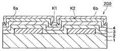
図14に本発明の第4実施形態に係る有機EL素子200の部分的な概略断面構成を示す。上記各実施形態では、保護層6はALE法のみにより成膜されたものであったが、本実施形態は、構造体2〜5の上に形成された保護層6を、ALE法により形成された層(ALE層という)6aと、ALE法とは異なる方法により形成された層(非ALE層という)6bとの組合せから構成したことを特徴とするものである。
【0101】
本例では、保護層6は、厚さ数nm〜数十nmのAl2O3よりなるALE層6aと厚さ数nm〜数十nmのCVD法により形成されたAl2O3よりなる非ALE層6bとが交互に積まれたものである。ここで、ALE層6aが構造体2〜5の直上に形成され、非ALE層6bがALE層6aの上に形成され、以降、順次交互に積層されている。なお、図示例では4層だが層数は限定しない。
【0102】
次に、本実施形態の保護層6の形成方法について述べる。図15は、本実施形態に係る成膜装置の模式的な構成を示す図である。この成膜装置は、まず、ALE法によりALE層6aであるAl2O3膜を形成し、続いて、同じ装置内にて、CVD法により非ALE層6bであるAl2O3膜を形成するものである。
【0103】
10は例えばステンレス等より区画形成された密閉構造の真空室であり、その内部は排気通路11とつながっている。そして、真空室10の内部は、図示しない真空ポンプ(メカニカルブースターポンプやロータリーポンプ等)を用いて、排気通路11から真空に引かれている。
【0104】
真空室10の内部には、例えばチタン等により密閉構造に形成された反応室12が設置されている。反応室12の壁部には、図示しない制御回路等にて作動制御される電動開閉式のシャッタ13が形成されている。このシャッタ13を開閉することで反応室12内への基板の出し入れを行ったり、シャッタ13の開度調整によって反応室12内の圧力を調整したり、シャッタ13を全開することでパージの促進を行うようになっている。
【0105】
また、反応室12内へTMAガス、H2Oガス及びN2ガスを供給するためのステンレス等よりなる各配管系14、15、16、17が設けられている。配管系14はTMAガスの配管系(TMA配管系)であり、反応室12内へTMAガスを導入するためのものである。配管系15はN2ガスの配管系(TMA除去用N2ガス配管系)であり、TMA配管系14によってTMAガスを所定の時間流した後に、残存するTMAガスを除去するためのパージガスとしてのN2ガスを流すために利用する。
【0106】
配管系16は反応ガスであるH2Oガスの配管系(水配管系)であり、TMA除去用N2ガス配管系15によってパージガスを流した後、反応室12内へH2Oガスを導入するためのものである。配管系17はN2ガスの配管系(水除去用N2ガス配管系)であり、水配管系16によってH2Oガスを所定の時間流した後に、残存するH2Oガスを除去するためのパージガスとしてのN2ガスを流すために利用する。
【0107】
これらTMA配管系14、水配管系16、各N2ガス配管系15、17は各々、図示しない制御回路等によって作動制御される図示しないバルブ及びガス供給源を有しており、それぞれ、吸着ガス供給手段、反応ガス供給手段、パージ手段を構成している。
【0108】
そして、各配管系14〜17のバルブは、所定のタイミングにて開閉されるようになっており、それによって、反応室12へのガス供給は、TMA、N2ガス(パージガス)、H2Oガス、N2ガス(パージガス)の順に、切り替えて交互に供給されるようになっている。なお、配管系14〜17は、真空室10を貫通して(貫通部は密封構造となっている)、接続用のボルト等により反応室12に接続されている。
【0109】
また、反応室12の内部には、薄膜が形成される基板(ガラス基板等)18を搭載するヒータ付き基板ホルダ19が設置されている。この基板18は、上記各実施形態における構造体2〜5までが形成されたガラス基板1に相当するものである。基板ホルダ19は、例えば、基板18が搭載可能な面積を有する金属板の下に均一加熱可能なようにシースヒータを取り付けたものとできる。
【0110】
更に、基板ホルダ19は、基板温度を測定するための図示しない熱電対を有しており、図示しない温度制御回路によって該熱電対の測定値を検知しつつ、基板18を所望の温度に加熱可能となっている。また、この基板ホルダ19は、反応室12内へ基板18を出し入れするために、搬送可能になっている。
【0111】
かかる成膜装置においては、まず、基板18をヒータ付き基板ホルダ19に設置搭載し、真空室10を通して、シャッタ13の部分から反応室12内に搬送する。そこで、所望の反応が起こる以上の温度(本例では100℃)まで、基板18を基板ホルダ19により、加熱する。
【0112】
基板18が所望の温度(例えば100℃)に達したら、TMA配管系14からTMAガスを反応室12に送り込む。その供給流量、及び、TMA配管系14とは逆側にあるシャッタ13の開閉度を適宜制御することにより、反応室12内の雰囲気圧を数百Pa程度に保つことができ、基板18にTMAが一層だけ吸着する。その後、シャッタ13を全開にして、TMA除去用N2ガス配管系15よりN2ガスを流すことにより、反応室12内に残留するTMAガスを除去することができる。
【0113】
次に、H2Oガスを水配管系16から反応室12へ送り込む。その供給流量、及び、水配管系16とは逆側にあるシャッタ13の開閉度を適宜制御することにより、反応室12内の水蒸気圧を一定に保つことができ、基板18に吸着したTMAと反応させてAl2O3を形成することができる。その後、シャッタ13を全開にして、水除去用N2ガス配管系17よりN2ガスを流す。それにより、反応室12内に残留するH2Oを除去することができる。
【0114】
このようにALE法による成膜サイクル(TMA導入→パージ→H2O導入→パージ)を所望の膜厚に達するまで繰り返し、1層目のALE層6aを形成した後、以下のようなCVD法による成膜を開始する。なお、CVD成膜における成膜温度(基板温度)は、上記ALE法による成膜温度と同じ100℃とするが、これに限定するものではなく、室温でもよい。
【0115】
まず、TMAを気化して、そのガスをTMA配管系14から反応室12に送り込む。そのTMAガスの量を制御するとともに、TMA配管系14と逆側にあるシャッタ13の開閉度を制御して、反応室12の雰囲気圧を数百Pa以上に保つ。そうすると、TMAが基板18に吸着するのはもとより、基板18周辺に滞留する。
【0116】
その後、上記シャッタ13を全開にして、TMA除去用N2ガス配管系15より窒素ガスを流すこと無く、H2Oを気化して、そのガスを水配管系16から反応室12に送り込む。そうすると、基板18上はもとより、基板18周辺の気相でもTMAとH2Oとが反応して、Al2O3を形成することができる。こうして、基板18においてALE層6a上に、非ALE層6bが形成される。このようなCVD成膜では、成膜レートが速いため、膜中の空孔が成膜途中で消滅することが少なく、内部応力を低減できる。
【0117】
このように、本実施形態によれば、保護層6をALE法により成膜されたALE層6aとCVD法により成膜された非ALE層6bとの組み合わせにより構成しているため、互いの層6a、6bの膜質を変えることができ、ALE層6aを上記非応力緩和膜として、非ALE層6bを上記応力緩和膜としてそれぞれ機能させることができる。
【0118】
ALE層6aの内部応力は100℃程度の低温で成膜しても、例えば400nmの厚さで約430MPaになるが、CVD法により成膜された非ALE層6bでは−150Mpa程度に落とすことができる。従って、ALE層6aと非ALE層6bとの多層膜よりなる保護層6全体の全応力は、例えば400nmの厚さで150MPa程度に落とすことができる。
【0119】
また、応力緩和膜として機能する非ALE層6bは、膜内に内部欠陥等の多い膜となるので構造体2〜5に対する被覆性が不十分となりやすい。しかし、本実施形態の有機EL素子200によれば、図16に示す様に、非ALE層6bにカバレッジ不良部K1やピンホールK2が発生しても、その下、即ち、構造体2〜5の直上を被覆するALE層6aの被覆性が良いため、水分に対する抵抗性は問題ない。なお、図16は、上記図2において陰極5が無い部分の断面に対応した断面図である。
【0120】
よって、本実施形態においても、保護層6に発生する応力を緩和して亀裂等の損傷の可能性を低減した保護層6を実現することができ、保護層6の構造体2〜5に対する被覆性を、より確実に向上させることができる。さらに、本実施形態によれば、保護層6の一部を成膜レートの速いCVD法により形成するため、保護層6の全部をALE法にて成膜する場合に比べて、成膜時間を短くすることができる。なお、ALE法とは異なる方法はスパッタ法等でも良い。
【0121】
(第5実施形態)
図17に本発明の第5実施形態に係る有機EL素子300の部分的な概略断面構成(上記図16に対応した断面)を示す。本実施形態は、上記第4実施形態を変形したもので、第4実施形態とは、構造体2〜5に対するALE層6aと非ALE層6bの積層順を逆にしたものである。即ち、図17に示す様に、非ALE層6bが構造体2〜5の直上に形成され、ALE層6aが非ALE層6bの上に形成された2層構造としている。
【0122】
ここで、本実施形態の保護層6の形成方法の一例を述べる。まず、大気開放による有機発光材料の劣化を極力防ぐために、構造体2〜5を形成したものと同一の真空蒸着機内で、抵抗加熱蒸着法により、厚さ200nmのGeO(酸化ゲルマニウム)を非ALE層6bとして形成した。続いて、この非ALE層6bの上に、上記図3に示す形成方法と同様にして、TMAとH2Oを原材料としたALE法により、厚さ400nmのAl2O3をALE層6aとして成膜した。
【0123】
なお、非ALE層6bとしてはGeOに限ったものではなく、比較的低温での蒸着が可能なSiO、LiF、AlF3などの無機膜でもよい。また、非ALE法による成膜としては、構造体2〜5を形成したものと同一の真空蒸着機でなくても良い。
【0124】
また、ガラス基板1上に構造体2〜5を真空蒸着により形成した後、大気開放することなく、別の成膜装置に素子を搬送可能な機構を備えた成膜装置により、非ALE層6bを成膜するならば、その成膜法(非ALE法)も蒸着法に限定しない。例えば、陽極2から陰極5までを真空蒸着機にて成膜した後、大気開放することなくCVD装置に搬送し、Si1-XNXを非ALE層6bとして成膜することも可能である。
【0125】
また、CVD法の場合はガス圧等による成膜条件により、非ALE層6bに発生する応力を調整し易いという利点も生かされる。なんとなれば、ALE層6aを構成するAl2O3等は、上述のように引っ張り応力を示す傾向があるので、Si1-XNXを圧縮応力とすれば、これら引っ張り応力と圧縮応力とが相殺して保護層6の損傷や剥離の防止を図れるからである。
【0126】
また、非ALE層6bは、無機膜に限定されるものではなく、パラキシレン重合体、ポリイミドといった有機膜を用いてもよい。特に、これら有機膜は弾性率が極めて低いので、上層のALE層6a(Al2O3等)に発生する引っ張り応力を緩和できるという利点がある。
【0127】
ただし、これら有機膜は極性が弱いために、反応ガスの化学吸着を前提とするALE法においては、これら有機膜の上には膜が成長し難い、もしくは、有機膜とALE法による膜との界面の密着力が弱くなる懸念がある。従って、非ALE層6bとしての有機膜の上に、ALE層6aを形成するに先立っては、シランカップリング剤など適当なカップリング剤を用いることが望ましい。
【0128】
また、非ALE層6bとして、これら有機膜を適用する場合の別の懸念点としては、無機膜に比べて耐湿性が劣ることと、化学的・物理的安定性が劣ることである。従って、ALE層6aの成膜用装置に有機EL素子を移し替えるときに、やむなく一度大気開放せざるを得ないような場合、大気の湿度による有機EL素子の特性劣化を予防するために、少なくとも非ALE層6bとしての有機膜は1μm程度の厚さを確保して成膜しておくことが望ましい。ただし、この厚さは大気開放する時間、大気中の湿度に依存する。
【0129】
また、非ALE層6bとしての有機膜が、その上に、ALE層6aをALE法により成膜するときの原料ガスにより侵され、該有機膜の直下の有機発光材料3、4に原料ガスのダメージが生じてしまうことを回避するためにも、非ALE層6bとしての有機膜は、1μm程度の厚さに成膜しておくのが望ましい。
【0130】
このように、本実施形態によっても、上記第4実施形態と同様に、保護層6をALE層6aと非ALE層6bとの組み合わせにより構成しているため、互いの層6a、6bの膜質を変えることができ、ALE層6aを上記非応力緩和膜として、非ALE層6bを上記応力緩和膜としてそれぞれ機能させることができる。
【0131】
また、上記図17に示す様に、非ALE層6bにカバレッジ不良部K1やピンホールK2が発生しても、その上を被覆するALE層6aの被覆性が良いため、水分に対する抵抗性は問題ない。つまり、ALE層6aにより、保護層6の被覆性が確保される。
【0132】
よって、本実施形態においても、保護層6に発生する応力を緩和して亀裂等の損傷の可能性を低減した保護層6を実現することができ、保護層6の構造体2〜5に対する被覆性を、より確実に向上させることができる。さらに、本実施形態においても、保護層6の全部をALE法にて成膜する場合に比べて、成膜時間を短くすることができる。
【0133】
(他の実施形態)
なお、有機発光材料としてのホール輸送層や有機発光層は上記のものに限定されるものではなく、公知の材料等を適宜使用することができる。さらには、一対の電極間に有機発光材料としてのホール輸送層及び有機発光層を挟んでなるものに限らず、ホール注入層、電子輸送層や電子注入層等(これらも有機発光材料に相当する)が適宜存在するものでも良い。
【図面の簡単な説明】
【図1】本発明の第1実施形態に係る有機EL素子の部分断面図である。
【図2】図1に示す有機EL素子の概略平面図である。
【図3】上記第1実施形態に係る保護層の形成方法の一例を示す流れ図である。
【図4】ALE法による保護層の成膜温度と有機EL素子の電圧−輝度特性との関係を示す図である。
【図5】保護層を保護する膜を設けた有機EL素子の部分断面図である。
【図6】上記第1実施形態における保護層の被覆性向上効果を具体的に示す図である。
【図7】保護層の被覆性向上による非発光領域の抑制効果を示す図である。
【図8】本発明の第2実施形態に係る保護層の形成方法の一例を示す流れ図である。
【図9】上記第2実施形態における保護層の応力低減効果を示す図である。
【図10】本発明の第3実施形態に係る保護層の形成方法の一例を示す流れ図である。
【図11】図10に示す形成方法にて形成した保護層の応力低減効果を示す図である。
【図12】上記第3実施形態に係る保護層の形成方法の他の例を示す流れ図である。
【図13】図12に示す形成方法にて形成した保護層の応力低減効果を示す図である。
【図14】本発明の第4実施形態に係る有機EL素子の部分断面図である。
【図15】上記第4実施形態に係る成膜装置の構成図である。
【図16】上記第4実施形態に係る保護層の被覆性向上効果を示す概略断面図である。
【図17】本発明の第5実施形態に係る有機EL素子の部分断面図である。
【符号の説明】
1…ガラス基板、2…陽極、3…ホール輸送層、4…有機発光層、5…陰極、6…保護層、6a…ALE層、6b…非ALE層。[0001]
BACKGROUND OF THE INVENTION
The present invention includes an organic EL (electroluminescence) having a structure in which an organic light emitting material is disposed between a pair of electrodes facing each other on a substrate, and a protective layer that covers the organic light emitting material on the outer surface of the structure. elementAnd manufacturing method thereofAbout.
[0002]
[Prior art]
In general, an organic EL element includes a structure in which an organic light emitting material is disposed between a pair of electrodes facing each other on a substrate. However, the organic light emitting material deteriorates due to moisture in the use atmosphere, and a non-light emitting region is formed in the original light emitting region of the structure, leading to deterioration of display quality. To solve this problem, Japanese Patent Application Laid-Open No. 7-161474 discloses an inorganic amorphous film made of carbon or silicon formed by a CVD method (chemical vapor deposition method) and an organic light emitting material on the outer surface of the structure. It has been proposed to form it so as to cover it and use it as a protective film.
[0003]
[Problems to be solved by the invention]
However, according to the study by the present inventors conducted on the above-mentioned conventional publication, the conventional protective film has insufficient coverage with respect to the structure, and thus has low resistance to moisture, and high temperature and high humidity (for example, 65 It was found that when operated in an atmosphere at 95 ° C., a non-light-emitting region was generated.
[0004]
In view of the above problems, the present invention has a structure in which an organic light emitting material is disposed between a pair of electrodes facing each other on a substrate, and has a protective layer that covers the organic light emitting material on the outer surface of the structure. An object of the organic EL element is to improve the coverage of the protective layer on the structure.
[0005]
[Means for Solving the Problems]
In order to achieve the above object, in the invention according to
[0006]
The atomic layer growth method (hereinafter referred to as the ALE method in this section) utilizes the reaction on the surface of the object to be formed, so that a uniform film can be formed along the surface shape of the object to be formed. For this reason, the protective layer formed by the ALE method has better coverage with respect to the structure than a film formed by the conventional CVD method or the like. Therefore, according to the present invention, it is possible to improve the coverage of the protective layer on the structure. Further, if the covering property of the protective layer to the structure is improved, the resistance to moisture can be improved, so that a non-light-emitting region can be prevented from being formed in the structure by moisture.Further, if the protective layer contains a stress relaxation component for relaxing the stress generated in the protective layer, the stress generated in the protective layer is relaxed, and damage such as cracks is generated in the protective layer. Can be avoided.
[0007]
The invention of
[0008]
The invention according to
[0009]
Further, the invention of
[0010]
The stress can be relaxed by the stress relaxation film. In addition, since the stress relaxation film is usually a film with many internal defects, the coverage with respect to the structure tends to be insufficient, but in this respect, the non-stress relaxation film with few internal defects has a better coverage. Can be secured. Therefore, the stress which generate | occur | produces in a protective layer can be relieve | moderated and the protective layer which reduced the possibility of damages, such as a crack, can be implement | achieved, The effect of the invention of Claims 1-3 can be implement | achieved in a higher level it can.
[0011]
Here, the layers having different stresses generated inside each other can be formed by making the film forming conditions in the ALE method different from each other (invention of claim 5). Since the film quality can be changed by changing the film formation conditions (film formation temperature and the like), it is possible to form a stress relaxation film and a non-stress relaxation film having different stresses. The stress relaxation film and the non-stress relaxation film may be the same material or different materials.
[0013]
Where the claim1As a protective layerIsClaim6As in the present invention, a laminated structure in which a layer containing a stress relaxation component and a layer not containing a stress relaxation component may be laminated. According to this, since the layer containing the stress relaxation component functions as the stress relaxation film and the layer not containing the stress relaxation component functions as the non-stress relaxation film, the same effect as the invention of
[0014]
Claims6'sThe layer containing the stress relaxation component in the invention is claimed7In the film formation by the ALE method, the material gas constituting the protective layer (6) is used together with a gas containing an elemental component that acts as a stress relaxation component, unlike the material gas. You can do it. Specifically, a nitrogen compound gas containing a nitrogen element as an element component acting as a stress relaxation component can be used.
[0015]
Further, in realizing a protective layer that reduces the possibility of damage such as cracks by relaxing the stress generated in the protective layer, claims9As in the present invention, the protective layer (6) is a combination of a layer (6a) formed by the ALE method and a layer (6b) formed by a method different from the ALE method (hereinafter referred to as non-ALE method). It may be configured from
[0016]
Thereby, the film quality of each other layer can be changed, and the layer formed by the ALE method can function as the stress relaxation film, and the layer formed by the non-ALE method can function as the non-stress relaxation film. The same effect as that of the invention of
[0017]
Here, as a combination of a layer formed by the ALE method (ALE layer) and a layer formed by the non-ALE method (non-ALE layer), the claims10The non-ALE layer (6b) may be formed directly on the structure (2-5) and the ALE layer (6a) may be formed on the non-ALE layer (6b), or vice versa.11As in the present invention, the ALE layer (6a) may be formed immediately above the structures (2 to 5), and the non-ALE layer (6b) may be formed thereon.In the organic EL device according to
[0018]
The invention according to
While alternately introducing a first gas containing an organometallic component and a second gas containing oxygen into the reaction furnace, the temperature of the glass substrate in the reaction furnace is set to be equal to or lower than the glass transition point of the organic light emitting material. The first layer of the protective layer is formed by the first gas and the second gas by controlling to be the first temperature, and after the formation of the first layer, the reaction By controlling the temperature of the glass substrate in the furnace to be a second temperature that is different from the first temperature and lower than or equal to the glass transition point of the organic light-emitting material, Forming the second layer of the protective layer with the gas and the second gas,
The protective layer having a desired thickness as the metal oxide containing the organometallic component is formed by repeatedly introducing the first gas and the second gas a plurality of cycles. The first gas is made of trimethylaluminum, and the second gas is vaporized H2O
By making the second temperature of the glass substrate higher than the first temperature, the first layer is an alumina film as a stress relaxation film, and the second layer is a non-stress relaxation film. It is characterized by using an alumina film.In addition, the code | symbol in the bracket | parenthesis of each said means is an example which shows a corresponding relationship with the specific means as described in embodiment mentioned later.
[0019]
DETAILED DESCRIPTION OF THE INVENTION
DESCRIPTION OF THE PREFERRED EMBODIMENTS Embodiments shown in the drawings will be described below. In the following embodiments, the same parts are denoted by the same reference numerals in the drawings.
[0020]
(First embodiment)
FIG. 1 is a partial cross-sectional view of an organic EL (electroluminescence)
[0021]
[0022]
On the
[0023]
On the organic
[0024]
As described above, the
[0025]
As described above, the
[0026]
As shown in FIG. 2 (for the sake of convenience, the
[0027]
In such an
[0028]
By the way, in this embodiment, in the
[0029]
First, a quartz glass mask was fixed on a glass substrate (glass substrate with an organic EL thin film) 1 on which an
[0030]
After that, TMA (trimethylaluminum) was placed in the raw material bottle at 28 ° C., H2O is kept at room temperature (24 ° C.) in the raw material bottle, vaporized under reduced pressure, and N is a carrier gas as follows.2Gas (flow rate was 400 sccm) was alternately introduced into the reactor. First, after introducing vaporized TMA for 0.6 seconds, in order to remove excess TMA present in the gas phase other than the molecules adsorbed on the substrate surface, N2 is used as a purge gas.2Gas was introduced for 2.4 seconds. After that, vaporize H as well2O for 1.0 second, N2The purge gas was deposited at a gas introduction time (pulse time) of 4.0 seconds.
[0031]
This TMA introduction → purge → H2Film formation was performed by repeating the cycle of O introduction → purging 5000 times (about 11 hours). During this time, the pressure in the reaction furnace was 150 to 300 Pa, and the substrate temperature was maintained at 100 ° C. by a heater in the reaction furnace. After film formation is completed, N2Cooling was performed while introducing 400 sccm of gas, and when the substrate temperature reached 70 ° C., the reactor was brought to atmospheric pressure, and the
[0032]
Here, with respect to the substrate temperature (deposition temperature) when forming the
[0033]
FIG. 4 is a graph showing the results of confirming how the voltage-luminance characteristics of the element change depending on the film formation temperature (substrate temperature). Almost no difference was observed when the film was formed at a film forming temperature of 100 ° C. and when the film was formed at 130 ° C. (Tg point of TPTE). It can be seen that the luminance characteristic is shifted to the right. This is presumably because the crystallization of TPTE progressed during the process of forming the
[0034]
Next, points to be noted regarding the film thickness, composition, processing, and film forming apparatus in the ALE method of the
[0035]
[Thickness of Protective Layer] In this embodiment, the
[0036]
In the ALE method, since the step coverage rate is almost 100% if the gas substrate adsorption rate is uniform, even if the substrate surface is clean, even if it is thin, pinholes and defects are generated. The organic
[0037]
Further, in order to protect against scratches at the time of substrate processing and physical damage during assembly at the product level, after the
[0038]
Here, the composition, film forming method, and thickness of the
[0039]
[Composition of Protective Layer] The
[0040]
The raw material for obtaining the
[0041]
For example, in order to obtain the
[0042]
Further, in the ALE method, if the reaction efficiency is improved by irradiating UV (ultraviolet rays) from the substrate to further activate the chemical reaction, the film is formed at a lower temperature below the Tg point of the
[0043]
In addition, when forming a film on the organic
[0044]
For example, when the organic
[0045]
[Processing of Protective Film] As described above, the connection terminal portions (electrode extraction portions) 2a and 5a of the cathode (upper electrode) 5 and the anode (lower electrode) 2 of the
[0046]
Here, even if the mask is not made of quartz glass, it is only necessary to achieve the purpose of preventing the
[0047]
In this case, it is preferable to apply a pressure from the outside so that the mask and the substrate are in close contact with each other, or to apply a treatment such as reverse taper processing to the mask end portion to make it difficult for gas to flow around. In addition, as long as the heat resistance of the mask material allows for the substrate temperature, an organic material such as a rubber material or an epoxy resin may be used to form a mask by a coating method, a screen printing method, a spin coating method, or the like. Good.
[0048]
Further, a
[0049]
[Film Forming Apparatus] The
[0050]
By the way, according to this embodiment, the original structure which formed into a
[0051]
Therefore, according to this embodiment, the coverage with respect to the structures 2-5 of the
[0052]
Further, as shown in FIG. 5, if a
[0053]
Further, as described above, when the temperature at the time of film formation of the
[0054]
Next, although it does not limit, the effect of the coverage improvement with respect to the structures 2-5 of the
[0055]
The lifespan of these X, Y, and Z elements was compared by a high temperature and high humidity operation test. The test conditions were to operate in an atmosphere of 65 ° C. and 95% RH. FIG. 6 shows the luminance (cd / m) with the operating time (Hr) at that time.2). In addition, as the luminance measurement conditions at this time, the current was adjusted according to the decrease in the light emitting area, and the current density was made constant. As is clear from FIG. 6, the Y element (solid line) and the Z element (broken line) have a gradual decrease in luminance with respect to the X element (dashed line).
[0056]
FIG. 7 is a diagram schematically showing a light emitting region (one of the display pixels G) after 200 hours of operation in the high temperature and high humidity operation test. In FIG. 7, (a) is an initial state in each element of X, Y, and Z, (b) is a state after 200 hours of operation of the X element, and (c) is after 200 hours of operation of the Y element and Z element. Shows the state. Here, the dark spot D2 existing in FIG. 7A is caused by foreign matters such as dust originally existing on the organic
[0057]
From FIG. 7, in the Y and Z elements, the coverage of the
[0058]
(Second Embodiment)
By the way, normally, the
[0059]
Here, the stress generated in the
[0060]
In the second embodiment, in addition to the first embodiment, the
[0061]
For example, Al deposited by the ALE method2OThreeThe
[0062]
The formation of the
[0063]
For example, Al by the ALE method2OThreeIn order to contain N atoms as stress relaxation components, TMA or H which is a material gas constituting the
[0064]
(1) TMA introduction → purge → H2O + NHThreeIntroduction (H2O and NHThreeAnd a method of forming an AlxOyNz film as the
[0065]
As described above, the
[0066]
Where TMA and NHThreeIn the atomic layer growth of an AlN thin film by the above reaction, in general, the film formation temperature is desirably 300 ° C. or more from the viewpoint of a practical film formation rate and a complete reaction. It does not matter, and the reaction may not be uniform, so it may be at a low temperature. That is, the cycle procedure is not limited.
[0067]
However, since AlxOyNz and AlN may exhibit conductivity depending on their density, forming them directly on the
[0068]
Alternatively, when AlxOyNz or AlN is in direct contact with the
[0069]
When an AlxOyNz film is formed as the
[0070]
Next, although not limited, an example in which the stress reduction effect and the like of the
[0071]
First, the cleaned glass substrate 1 (35 mm × 45 mm) was placed in a reaction furnace. The reactor is evacuated to about 40 Pa and N2The
[0072]
The gas was introduced into the reactor as follows. First, after introducing vaporized TMA for 0.6 seconds, N2Gas was introduced for 2.4 seconds. Then, similarly, vaporization H2O for 0.6 seconds, N2Purge gas for 1.8 seconds, NHThreeGas for 1.0 second, N2Purge gas was sequentially introduced for 2.0 seconds to form a film. This TMA introduction → purge → H2O introduction → purge → NHThreeThe introduction → purge cycle was repeated 5000 times to form a film. During this time, the pressure in the reactor was 150 to 300 Pa, and the substrate temperature was maintained at 130 ° C. by a heater in the reactor.
[0073]
After film formation is completed, N2Cooling was performed while introducing 400 sccm of gas, and when the substrate temperature reached 70 ° C., the reactor was brought to atmospheric pressure, and the
[0074]
Further, from the deformation (warpage amount) before and after the film formation on the
[0075]
Therefore, according to the organic EL element to which the
[0076]
(Third embodiment)
Similarly to the second embodiment, the third embodiment also realizes the
[0077]
Specifically, the
[0078]
A film having a compressive stress (hereinafter,-(minus) is added to the numerical value of the stress) and a film having a tensile stress are combined, or films having a small stress regardless of compression or tension are combined, and the total stress is one layer. The number of layers and the composition ratio are not particularly limited. As a result, the total stress of the
[0079]
If given as a numerical value, empirically, the total stress is desirably −150 MPa to 150 MPa, and more specifically, −50 MPa to 50 MPa. Also, for example, when the constituent elements of films having different film forming conditions are the same, the film forming conditions such as the film forming temperature, the gas supply amount, the flow rate on the substrate, etc. are changed during the film forming, so Although they are composed of elements, films having different film qualities are stacked.
[0080]
TMA and H2Al from O to ALE method2OThreeFor example, when the substrate temperature (film formation temperature) is lowered to a low temperature of about 30 ° C. to 80 ° C., for example, the film is formed at a normal substrate temperature (for example, 100 ° C.). Also, a stress relaxation film with reduced stress can be formed. Furthermore, oxidation reaction gas H2The amount of O supplied may be reduced, for example, by shortening the introduction time, and the reaction rate may be reduced. In this case as well, a stress relaxation film can be formed.
[0081]
Here, if the substrate temperature is lowered, the amount of adsorption to the substrate is lowered, so it is better to increase the supply amount of TMA than at the normal substrate temperature. The supply amount can be easily increased by raising the temperature of the raw material bottle. When the film is formed in this way, a large amount of unreacted methyl groups and carbon should remain in the film and internal defects should be generated, whereby a stress relaxation film with reduced stress can be formed.
[0082]
Since the internal defects are very microscopic, pinholes and step coverage can be guaranteed if the substrate adsorption, which is the basis of ALE film formation, is ideal. In view of the reliability of the organic EL element, it is better to stack a denser thin film on the upper or lower part. In this case, the ALE may be continuously grown in the same reactor in a high temperature range of about 100 ° C. to 140 ° C.
[0083]
The thickness and thickness ratio of each layer formed under these different conditions are not limited. Further, since the number and structure of the layers are not limited, it is only necessary to combine a stress relaxation film having many internal defects and a non-stress relaxation film having few internal defects, and as a result, the total stress of the entire
[0084]
Further, the two or more
[0085]
Next, although not limited, the present embodiment will be described more specifically with reference to the following verification examples (first and second verification examples). In each of these verification examples, only the
[0086]
[First Verification Example] In this example, when the constituent elements of the films having different film forming conditions in the
[0087]
The cleaned glass substrate 1 (35 mm × 45 mm) is put in a reaction furnace, the reaction furnace is evacuated to about 40 Pa, N2The
[0088]
First, after introducing vaporized TMA for 0.6 seconds, N2Gas was introduced for 2.4 seconds. After that, vaporize H as well2O for 0.2 seconds, N2The purge gas was introduced at a gas introduction time (pulse time) of 2.0 seconds. This TMA introduction → purge → H2The film was formed by repeating the cycle of O introduction → purging 3000 times. During this time, the pressure in the reaction furnace was 150 to 300 Pa, and the substrate temperature was maintained at 50 ° C. by a heater in the reaction furnace.
[0089]
Then N2The substrate temperature was stabilized at 100 ° C. while introducing 400 sccm of gas. Thereafter, in the same pulse time as when the substrate temperature is 50 ° C., TMA introduction → purge → H2The film was formed by repeating the cycle of O introduction → purging 2000 times. After film formation is completed, N2Cooling was performed while introducing 400 sccm of gas, and when the substrate temperature reached 70 ° C., the reactor was brought to atmospheric pressure, and the
[0090]
As a result, the
[0091]
Therefore, according to the
[0092]
The stress can be relaxed by the stress relaxation film. In addition, as described above, the stress relaxation film with many internal defects and the like tends to have insufficient coverage with respect to the structure. However, in this respect, the non-stress relaxation film with few internal defects has a better coverage. It can be secured. Therefore, it is possible to realize the
[0093]
[Second Verification Example] In this example, films having different film forming conditions in the
[0094]
Then SiClFourAnd H2O is vaporized in the raw material bottle, and N is a carrier gas as follows.2Gas (flow
[0095]
Then N2The substrate temperature was stabilized at 100 ° C. while introducing 400 sccm of gas. After this, TMA and H2O is vaporized in the raw material bottle, and N is a carrier gas as follows.2Gas (flow
[0096]
After introducing vaporized TMA for 0.6 seconds, N2Gas was introduced for 2.4 seconds. After that, vaporize H as well2O for 0.2 seconds, N2The purge gas was introduced at a gas introduction time (pulse time) of 2.0 seconds. This TMA introduction → purge → H2The film was formed by repeating the cycle of O introduction → purging 2000 times to form SiO.2Al on the film2OThreeA film was formed. After film formation is completed, N2Cooling was performed while introducing 400 sccm of gas, and when the substrate temperature reached 70 ° C., the reactor was brought to atmospheric pressure, and the
[0097]
As a result, the
[0098]
Therefore, according to the
[0099]
In the second verification example, Al previously formed at a substrate temperature of 130 ° C.2OThreeThe film is a non-stress relaxation film, SiO formed later at a substrate temperature of 100 ° C.2The film becomes a stress relaxation film, and a stress relaxation effect is obtained by the stress relaxation film, and the covering property can be secured by the non-stress relaxation film. And the
[0100]
(Fourth embodiment)
FIG. 14 shows a partial schematic cross-sectional configuration of an
[0101]
In this example, the
[0102]
Next, a method for forming the
[0103]
[0104]
Inside the
[0105]
Also, TMA gas, H into the reaction chamber 122O gas and N2Each piping
[0106]
The
[0107]
These
[0108]
The valves of the
[0109]
A
[0110]
Further, the
[0111]
In such a film forming apparatus, first, the
[0112]
When the
[0113]
Next, H2O gas is sent from the
[0114]
Thus, the film formation cycle by ALE method (TMA introduction → purge → H2(O introduction → purging) is repeated until a desired film thickness is reached, and after the
[0115]
First, TMA is vaporized, and the gas is sent from the
[0116]
Thereafter, the
[0117]
As described above, according to the present embodiment, the
[0118]
Even if the internal stress of the
[0119]
Moreover, since the
[0120]
Therefore, also in the present embodiment, it is possible to realize the
[0121]
(Fifth embodiment)
FIG. 17 shows a partial schematic cross-sectional configuration (cross-section corresponding to FIG. 16) of an
[0122]
Here, an example of the formation method of the
[0123]
The
[0124]
Further, after the
[0125]
In the case of the CVD method, the advantage that the stress generated in the
[0126]
The
[0127]
However, since these organic films are weak in polarity, in the ALE method based on the chemical adsorption of the reaction gas, it is difficult for the film to grow on these organic films, or between the organic film and the film formed by the ALE method. There is a concern that the adhesion at the interface will be weakened. Therefore, it is desirable to use a suitable coupling agent such as a silane coupling agent before forming the
[0128]
Another concern when applying these organic films as the
[0129]
In addition, the organic film as the
[0130]
Thus, also in the present embodiment, as in the fourth embodiment, since the
[0131]
Further, as shown in FIG. 17, even if the coverage failure portion K1 or the pinhole K2 occurs in the
[0132]
Therefore, also in the present embodiment, it is possible to realize the
[0133]
(Other embodiments)
Note that the hole transport layer and the organic light emitting layer as the organic light emitting material are not limited to those described above, and known materials and the like can be appropriately used. Furthermore, the hole transport layer and the organic light emitting layer as an organic light emitting material are not only sandwiched between a pair of electrodes, but also a hole injection layer, an electron transport layer, an electron injection layer, etc. (these also correspond to the organic light emitting material) ) May be present as appropriate.
[Brief description of the drawings]
FIG. 1 is a partial cross-sectional view of an organic EL element according to a first embodiment of the present invention.
FIG. 2 is a schematic plan view of the organic EL element shown in FIG.
FIG. 3 is a flowchart showing an example of a method for forming a protective layer according to the first embodiment.
FIG. 4 is a diagram showing the relationship between the temperature at which a protective layer is formed by the ALE method and the voltage-luminance characteristics of an organic EL element.
FIG. 5 is a partial cross-sectional view of an organic EL element provided with a film for protecting a protective layer.
FIG. 6 is a diagram specifically showing the effect of improving the coverage of the protective layer in the first embodiment.
FIG. 7 is a diagram showing an effect of suppressing a non-light emitting region by improving the coverage of a protective layer.
FIG. 8 is a flowchart showing an example of a method for forming a protective layer according to the second embodiment of the present invention.
FIG. 9 is a diagram showing the stress reduction effect of the protective layer in the second embodiment.
FIG. 10 is a flowchart showing an example of a method for forming a protective layer according to a third embodiment of the present invention.
11 is a diagram showing a stress reduction effect of a protective layer formed by the forming method shown in FIG.
FIG. 12 is a flowchart showing another example of a method for forming a protective layer according to the third embodiment.
13 is a diagram showing the stress reduction effect of the protective layer formed by the forming method shown in FIG.
FIG. 14 is a partial cross-sectional view of an organic EL device according to a fourth embodiment of the invention.
FIG. 15 is a configuration diagram of a film forming apparatus according to the fourth embodiment.
FIG. 16 is a schematic cross-sectional view showing the effect of improving the coverage of the protective layer according to the fourth embodiment.
FIG. 17 is a partial cross-sectional view of an organic EL element according to a fifth embodiment of the invention.
[Explanation of symbols]
DESCRIPTION OF
Claims (16)
Translated fromJapanese前記構造体の外表面に、前記有機発光材料を被覆する保護層(6)を有し、この保護層が原子層成長法により形成されており、
前記保護層の全応力は−150MPa〜150MPaであり、
前記保護層は、該保護層に発生する応力を緩和するための応力緩和成分としての窒素を含有しているものであるか、または、異なる膜質の層が積層されてなるものであることを特徴とする有機EL素子。An organic EL element comprising a structure in which an organic light emitting material (3, 4) is disposed between a pair of electrodes (2, 5) facing each other on a substrate (1),
The outer surface of the structure has a protective layer (6) covering the organic light emitting material, and the protective layer is formed by an atomic layer growth method,
The total stress of the protective layer is −150 MPa to 150 MPa,
The protective layer contains nitrogen as a stress relaxation component for relieving stress generated in the protective layer, or is formed by laminating layers having different film qualities. An organic EL element.
前記構造体の外表面に、原子層成長法を用いて、有機発光材料を被覆する保護層(6)を形成する工程と、を備える有機EL素子の製造方法であって、 Forming a protective layer (6) covering the organic light emitting material on the outer surface of the structure using an atomic layer growth method, and a method for producing an organic EL element,
前記原子層成長法による前記保護層の形成工程では、前記構造体が形成された前記ガラス基板を、反応炉に入れて、その反応炉を真空にし、 In the step of forming the protective layer by the atomic layer growth method, the glass substrate on which the structure is formed is put into a reaction furnace, and the reaction furnace is evacuated,
有機金属成分を含む第1のガスと酸素を含む第2のガスとを前記反応炉に交互に導入しながら、前記反応炉内の前記ガラス基板の温度を、前記有機発光材料のガラス転移点以下である第1の温度となるように制御することにより、前記第1のガスおよび前記第2のガスにより前記保護層の第1の層を形成し、この第1の層の形成後、前記反応炉内の前記ガラス基板の温度を、前記第1の温度とは異なる温度であって且つ前記有機発光材料のガラス転移点以下である第2の温度となるように制御することにより、前記第1のガスおよび前記第2のガスにより前記保護層の第2の層を形成するものであり、 While alternately introducing a first gas containing an organometallic component and a second gas containing oxygen into the reaction furnace, the temperature of the glass substrate in the reaction furnace is set to be equal to or lower than the glass transition point of the organic light emitting material. The first layer of the protective layer is formed by the first gas and the second gas by controlling to be the first temperature, and after the formation of the first layer, the reaction By controlling the temperature of the glass substrate in the furnace to be a second temperature that is different from the first temperature and lower than or equal to the glass transition point of the organic light-emitting material, Forming the second layer of the protective layer with the gas and the second gas,
この第1および第2のガスを交互に導入することを複数サイクル繰り返し行うことによって、前記有機金属成分を含む金属酸化物としての所望厚さを有する前記保護層を形成するものであり、 The protective layer having a desired thickness as the metal oxide containing the organometallic component is formed by repeatedly introducing the first gas and the second gas a plurality of cycles.
前記第1のガスはトリメチルアルミニウムよりなり、前記第2のガスは気化したH The first gas is made of trimethylaluminum, and the second gas is vaporized H22Oよりなり、O
前記ガラス基板における前記第2の温度を前記第1の温度よりも高いものとすることにより、前記第1の層を応力緩和膜としてのアルミナ膜とし、前記第2の層を非応力緩和膜としてのアルミナ膜とすることを特徴とする有機EL素子の製造方法。 By making the second temperature of the glass substrate higher than the first temperature, the first layer is an alumina film as a stress relaxation film, and the second layer is a non-stress relaxation film. A method for producing an organic EL element, characterized by comprising an alumina film of
Priority Applications (3)
| Application Number | Priority Date | Filing Date | Title |
|---|---|---|---|
| JP2000101304AJP4556282B2 (en) | 2000-03-31 | 2000-03-31 | Organic EL device and method for manufacturing the same |
| US09/820,168US20010031379A1 (en) | 2000-03-31 | 2001-03-29 | Organic EL device with protective layer |
| US10/345,234US6933002B2 (en) | 2000-03-31 | 2003-01-16 | Method for manufacturing organic EL device with protective layer |
Applications Claiming Priority (1)
| Application Number | Priority Date | Filing Date | Title |
|---|---|---|---|
| JP2000101304AJP4556282B2 (en) | 2000-03-31 | 2000-03-31 | Organic EL device and method for manufacturing the same |
Publications (2)
| Publication Number | Publication Date |
|---|---|
| JP2001284042A JP2001284042A (en) | 2001-10-12 |
| JP4556282B2true JP4556282B2 (en) | 2010-10-06 |
Family
ID=18615385
Family Applications (1)
| Application Number | Title | Priority Date | Filing Date |
|---|---|---|---|
| JP2000101304AExpired - Fee RelatedJP4556282B2 (en) | 2000-03-31 | 2000-03-31 | Organic EL device and method for manufacturing the same |
Country Status (2)
| Country | Link |
|---|---|
| US (2) | US20010031379A1 (en) |
| JP (1) | JP4556282B2 (en) |
Cited By (1)
| Publication number | Priority date | Publication date | Assignee | Title |
|---|---|---|---|---|
| KR101671529B1 (en)* | 2008-01-30 | 2016-11-01 | 오스람 오엘이디 게엠베하 | Device comprising an encapsulation unit |
Families Citing this family (116)
| Publication number | Priority date | Publication date | Assignee | Title |
|---|---|---|---|---|
| US6620723B1 (en) | 2000-06-27 | 2003-09-16 | Applied Materials, Inc. | Formation of boride barrier layers using chemisorption techniques |
| US7405158B2 (en) | 2000-06-28 | 2008-07-29 | Applied Materials, Inc. | Methods for depositing tungsten layers employing atomic layer deposition techniques |
| US7732327B2 (en) | 2000-06-28 | 2010-06-08 | Applied Materials, Inc. | Vapor deposition of tungsten materials |
| US6551929B1 (en) | 2000-06-28 | 2003-04-22 | Applied Materials, Inc. | Bifurcated deposition process for depositing refractory metal layers employing atomic layer deposition and chemical vapor deposition techniques |
| US7101795B1 (en) | 2000-06-28 | 2006-09-05 | Applied Materials, Inc. | Method and apparatus for depositing refractory metal layers employing sequential deposition techniques to form a nucleation layer |
| US7964505B2 (en) | 2005-01-19 | 2011-06-21 | Applied Materials, Inc. | Atomic layer deposition of tungsten materials |
| US7476420B2 (en)* | 2000-10-23 | 2009-01-13 | Asm International N.V. | Process for producing metal oxide films at low temperatures |
| TW548239B (en)* | 2000-10-23 | 2003-08-21 | Asm Microchemistry Oy | Process for producing aluminium oxide films at low temperatures |
| US6825447B2 (en) | 2000-12-29 | 2004-11-30 | Applied Materials, Inc. | Apparatus and method for uniform substrate heating and contaminate collection |
| US6765178B2 (en) | 2000-12-29 | 2004-07-20 | Applied Materials, Inc. | Chamber for uniform substrate heating |
| US6998579B2 (en) | 2000-12-29 | 2006-02-14 | Applied Materials, Inc. | Chamber for uniform substrate heating |
| US6951804B2 (en) | 2001-02-02 | 2005-10-04 | Applied Materials, Inc. | Formation of a tantalum-nitride layer |
| US6878206B2 (en) | 2001-07-16 | 2005-04-12 | Applied Materials, Inc. | Lid assembly for a processing system to facilitate sequential deposition techniques |
| US6660126B2 (en) | 2001-03-02 | 2003-12-09 | Applied Materials, Inc. | Lid assembly for a processing system to facilitate sequential deposition techniques |
| US6734020B2 (en) | 2001-03-07 | 2004-05-11 | Applied Materials, Inc. | Valve control system for atomic layer deposition chamber |
| US6897477B2 (en)* | 2001-06-01 | 2005-05-24 | Semiconductor Energy Laboratory Co., Ltd. | Semiconductor device, manufacturing method thereof, and display device |
| US7211144B2 (en) | 2001-07-13 | 2007-05-01 | Applied Materials, Inc. | Pulsed nucleation deposition of tungsten layers |
| EP1425110B1 (en)* | 2001-07-18 | 2014-09-03 | The Regents of the University of Colorado | A method of depositing an inorganic film on an organic polymer |
| US7085616B2 (en) | 2001-07-27 | 2006-08-01 | Applied Materials, Inc. | Atomic layer deposition apparatus |
| US6936906B2 (en) | 2001-09-26 | 2005-08-30 | Applied Materials, Inc. | Integration of barrier layer and seed layer |
| US7049226B2 (en) | 2001-09-26 | 2006-05-23 | Applied Materials, Inc. | Integration of ALD tantalum nitride for copper metallization |
| US7780785B2 (en) | 2001-10-26 | 2010-08-24 | Applied Materials, Inc. | Gas delivery apparatus for atomic layer deposition |
| US6916398B2 (en) | 2001-10-26 | 2005-07-12 | Applied Materials, Inc. | Gas delivery apparatus and method for atomic layer deposition |
| US6729824B2 (en) | 2001-12-14 | 2004-05-04 | Applied Materials, Inc. | Dual robot processing system |
| JP2003207965A (en)* | 2002-01-16 | 2003-07-25 | Seiko Epson Corp | Image forming device |
| US6815723B2 (en)* | 2001-12-28 | 2004-11-09 | Semiconductor Energy Laboratory Co., Ltd. | Light emitting device, method of manufacturing the same, and manufacturing apparatus therefor |
| US6620670B2 (en) | 2002-01-18 | 2003-09-16 | Applied Materials, Inc. | Process conditions and precursors for atomic layer deposition (ALD) of AL2O3 |
| US6926572B2 (en) | 2002-01-25 | 2005-08-09 | Electronics And Telecommunications Research Institute | Flat panel display device and method of forming passivation film in the flat panel display device |
| KR100507463B1 (en)* | 2002-01-25 | 2005-08-10 | 한국전자통신연구원 | Flat panel display and method for forming a passivation layer in flat panel display |
| US6998014B2 (en) | 2002-01-26 | 2006-02-14 | Applied Materials, Inc. | Apparatus and method for plasma assisted deposition |
| US6911391B2 (en) | 2002-01-26 | 2005-06-28 | Applied Materials, Inc. | Integration of titanium and titanium nitride layers |
| US6827978B2 (en) | 2002-02-11 | 2004-12-07 | Applied Materials, Inc. | Deposition of tungsten films |
| US6833161B2 (en) | 2002-02-26 | 2004-12-21 | Applied Materials, Inc. | Cyclical deposition of tungsten nitride for metal oxide gate electrode |
| JP2003272834A (en)* | 2002-03-20 | 2003-09-26 | Denso Corp | Display device |
| JP3501148B2 (en)* | 2002-03-25 | 2004-03-02 | 富士電機ホールディングス株式会社 | Organic EL display |
| JP2003282242A (en)* | 2002-03-25 | 2003-10-03 | Toyota Central Res & Dev Lab Inc | Organic electroluminescent element and organic electronic device |
| US7439191B2 (en) | 2002-04-05 | 2008-10-21 | Applied Materials, Inc. | Deposition of silicon layers for active matrix liquid crystal display (AMLCD) applications |
| DE10222958B4 (en)* | 2002-04-15 | 2007-08-16 | Schott Ag | Process for producing an organic electro-optical element and organic electro-optical element |
| US7279432B2 (en) | 2002-04-16 | 2007-10-09 | Applied Materials, Inc. | System and method for forming an integrated barrier layer |
| JP4048830B2 (en)* | 2002-05-16 | 2008-02-20 | 株式会社デンソー | Organic electronic device elements |
| JP2004014311A (en)* | 2002-06-07 | 2004-01-15 | Sony Corp | Method of forming organic thin film |
| JP3729262B2 (en) | 2002-08-29 | 2005-12-21 | セイコーエプソン株式会社 | ELECTROLUMINESCENT DEVICE AND ELECTRONIC DEVICE |
| JP2004095482A (en)* | 2002-09-03 | 2004-03-25 | Chi Mei Electronics Corp | Image display device |
| JP4032909B2 (en)* | 2002-10-01 | 2008-01-16 | ソニー株式会社 | Manufacturing method of organic light emitting display device |
| JP3953404B2 (en)* | 2002-10-21 | 2007-08-08 | インターナショナル・ビジネス・マシーンズ・コーポレーション | ORGANIC ELECTROLUMINESCENCE ELEMENT, METHOD FOR PRODUCING THE ORGANIC ELECTROLUMINESCENCE ELEMENT, AND ORGANIC ELECTROLUMINESCENCE DISPLAY DEVICE |
| JP3997888B2 (en)* | 2002-10-25 | 2007-10-24 | セイコーエプソン株式会社 | Electro-optical device, method of manufacturing electro-optical device, and electronic apparatus |
| JP4225030B2 (en)* | 2002-10-30 | 2009-02-18 | コニカミノルタホールディングス株式会社 | Organic electroluminescence device |
| KR100522427B1 (en)* | 2002-12-30 | 2005-10-20 | 주식회사 하이닉스반도체 | Method of manufacturing capacitor for semiconductor device |
| US7262133B2 (en) | 2003-01-07 | 2007-08-28 | Applied Materials, Inc. | Enhancement of copper line reliability using thin ALD tan film to cap the copper line |
| US6888172B2 (en)* | 2003-04-11 | 2005-05-03 | Eastman Kodak Company | Apparatus and method for encapsulating an OLED formed on a flexible substrate |
| US7192849B2 (en)* | 2003-05-07 | 2007-03-20 | Sensor Electronic Technology, Inc. | Methods of growing nitride-based film using varying pulses |
| KR20060006840A (en)* | 2003-05-16 | 2006-01-19 | 이 아이 듀폰 디 네모아 앤드 캄파니 | Barrier film for plastic substrate produced by atomic layer deposition |
| US7728516B2 (en) | 2003-06-13 | 2010-06-01 | Fuji Electric Holdings Co., Ltd. | Organic EL display |
| US7211508B2 (en) | 2003-06-18 | 2007-05-01 | Applied Materials, Inc. | Atomic layer deposition of tantalum based barrier materials |
| KR100569607B1 (en)* | 2003-08-26 | 2006-04-10 | 한국전자통신연구원 | Protective film formation method of organic light emitting element |
| KR100565636B1 (en)* | 2003-12-02 | 2006-03-30 | 엘지전자 주식회사 | Organic EL element and its manufacturing method |
| JP4131243B2 (en)* | 2004-02-06 | 2008-08-13 | セイコーエプソン株式会社 | Electro-optical device manufacturing method, electro-optical device, and electronic apparatus |
| US20050214556A1 (en)* | 2004-02-20 | 2005-09-29 | Fuji Photo Film Co., Ltd | Organic-inorganic composite composition, plastic substrate, gas barrier laminate film, and image display device |
| JP2007526601A (en)* | 2004-02-20 | 2007-09-13 | オー・ツェー・エリコン・バルザース・アクチェンゲゼルシャフト | Diffusion barrier layer and method for producing diffusion barrier layer |
| JP2005285659A (en)* | 2004-03-30 | 2005-10-13 | Toyota Industries Corp | Organic EL device and manufacturing method thereof |
| WO2006014591A2 (en)* | 2004-07-08 | 2006-02-09 | Itn Energy Systems, Inc. | Permeation barriers for flexible electronics |
| JP4363365B2 (en)* | 2004-07-20 | 2009-11-11 | 株式会社デンソー | Color organic EL display and manufacturing method thereof |
| JP2008077836A (en)* | 2005-01-12 | 2008-04-03 | Pioneer Electronic Corp | Organic EL panel |
| KR100819975B1 (en)* | 2005-01-19 | 2008-04-07 | 후지 덴키 홀딩스 가부시키가이샤 | Organic EL display |
| JP4425167B2 (en)* | 2005-03-22 | 2010-03-03 | 富士フイルム株式会社 | Gas barrier film, substrate film and organic electroluminescence device |
| KR20060104531A (en)* | 2005-03-30 | 2006-10-09 | 삼성에스디아이 주식회사 | Manufacturing method of light emitting display device |
| JP4663381B2 (en)* | 2005-04-12 | 2011-04-06 | 富士フイルム株式会社 | Gas barrier film, substrate film and organic electroluminescence device |
| JP4698310B2 (en)* | 2005-07-11 | 2011-06-08 | 富士フイルム株式会社 | Gas barrier film, substrate film and organic electroluminescence device |
| US7579285B2 (en)* | 2005-07-11 | 2009-08-25 | Imec | Atomic layer deposition method for depositing a layer |
| JP4363374B2 (en)* | 2005-08-04 | 2009-11-11 | 株式会社デンソー | Manufacturing method of color organic EL display |
| WO2007040295A1 (en)* | 2005-10-04 | 2007-04-12 | Seoul Opto Device Co., Ltd. | (al, ga, in)n-based compound semiconductor and method of fabricating the same |
| US7521858B2 (en)* | 2005-11-25 | 2009-04-21 | Toshiba Matsushita Display Technology Co., Ltd. | Organic EL display and method of manufacturing the same |
| KR100750591B1 (en) | 2005-12-07 | 2007-08-20 | 한국전자통신연구원 | Organic light-emitting device, method for manufacturing same, and method for forming inorganic insulating film for pixel electrode |
| JP4717674B2 (en) | 2006-03-27 | 2011-07-06 | 富士フイルム株式会社 | Gas barrier film, substrate film and organic electroluminescence device |
| US7781031B2 (en)* | 2006-12-06 | 2010-08-24 | General Electric Company | Barrier layer, composite article comprising the same, electroactive device, and method |
| US20080138538A1 (en)* | 2006-12-06 | 2008-06-12 | General Electric Company | Barrier layer, composite article comprising the same, electroactive device, and method |
| KR20080051572A (en)* | 2006-12-06 | 2008-06-11 | 주성엔지니어링(주) | Organic electroluminescent device and manufacturing method thereof |
| JP5220106B2 (en)* | 2007-06-22 | 2013-06-26 | ザ・リージエンツ・オブ・ザ・ユニバーシティ・オブ・コロラド | Protective coatings for organic electronic devices manufactured using atomic layer deposition and molecular layer deposition methods |
| KR100841679B1 (en) | 2007-07-12 | 2008-06-26 | 한양대학교 산학협력단 | Manufacturing method of protective film of organic device |
| DE102008014093B4 (en)* | 2007-12-27 | 2020-02-06 | Osram Opto Semiconductors Gmbh | Edge-emitting semiconductor laser chip with at least one current barrier |
| KR101509112B1 (en) | 2008-04-18 | 2015-04-08 | 삼성디스플레이 주식회사 | Organic light emitting display |
| JP2010198969A (en)* | 2009-02-26 | 2010-09-09 | Toshiba Mobile Display Co Ltd | Organic el display panel |
| KR101084267B1 (en)* | 2009-02-26 | 2011-11-16 | 삼성모바일디스플레이주식회사 | Organic light emitting display and manufacturing method thereof |
| DE102009024411A1 (en)* | 2009-03-24 | 2010-09-30 | Osram Opto Semiconductors Gmbh | Thin-film encapsulation for an optoelectronic component, method for its production and optoelectronic component |
| DE102009022900A1 (en) | 2009-04-30 | 2010-11-18 | Osram Opto Semiconductors Gmbh | Optoelectronic component and method for its production |
| DE102009034822A1 (en)* | 2009-07-27 | 2011-02-03 | Osram Opto Semiconductors Gmbh | Electronic component as well as electrical contact |
| JP5461096B2 (en)* | 2009-07-29 | 2014-04-02 | 双葉電子工業株式会社 | Organic EL display device |
| US20110083735A1 (en)* | 2009-10-13 | 2011-04-14 | Ips Ltd. | Solar cell and method of fabricating the same |
| EP2504872A1 (en)* | 2009-11-27 | 2012-10-03 | Koninklijke Philips Electronics N.V. | Organic electroluminescent devices |
| JP2011228648A (en)* | 2010-03-31 | 2011-11-10 | Fujifilm Corp | Imaging device |
| FR2958795B1 (en)* | 2010-04-12 | 2012-06-15 | Commissariat Energie Atomique | ORGANIC OPTOELECTRONIC DEVICE AND METHOD OF ENCAPSULATION |
| DE102010044738A1 (en)* | 2010-09-08 | 2012-03-08 | Osram Opto Semiconductors Gmbh | Thin-film encapsulation, optoelectronic semiconductor body with a thin-layer encapsulation and method for producing a thin-layer encapsulation |
| JP5589706B2 (en)* | 2010-09-17 | 2014-09-17 | カシオ計算機株式会社 | Light emitting device |
| JPWO2012039310A1 (en)* | 2010-09-22 | 2014-02-03 | 株式会社アルバック | Organic EL element manufacturing method, film forming apparatus, and organic EL element |
| JP5648523B2 (en)* | 2011-02-16 | 2015-01-07 | 富士通株式会社 | Semiconductor device, power supply device, amplifier, and semiconductor device manufacturing method |
| KR20120109083A (en) | 2011-03-24 | 2012-10-08 | 삼성디스플레이 주식회사 | Organic light emitting diode display and manufacturing method of organic light emitting diode display |
| WO2013051070A1 (en)* | 2011-10-07 | 2013-04-11 | パナソニック株式会社 | Light-emitting element and light-emitting element manufacturing method |
| JPWO2013051071A1 (en)* | 2011-10-07 | 2015-03-30 | パナソニック株式会社 | Light emitting device and method for manufacturing light emitting device |
| KR101717333B1 (en) | 2011-10-07 | 2017-03-16 | 가부시키가이샤 제이올레드 | Light-emitting element and light-emitting element manufacturing method |
| KR20140096982A (en)* | 2011-11-22 | 2014-08-06 | 파나소닉 주식회사 | Method for manufacturing display palel, display panel and display device |
| JP5687638B2 (en)* | 2012-01-26 | 2015-03-18 | 株式会社東芝 | Manufacturing method of display device |
| KR101931177B1 (en)* | 2012-03-02 | 2018-12-21 | 삼성디스플레이 주식회사 | Organic light emitting display device |
| JP5674707B2 (en)* | 2012-05-22 | 2015-02-25 | 株式会社東芝 | Display device |
| WO2015192144A2 (en)* | 2014-06-13 | 2015-12-17 | Hzo, Inc. | Protective coatings for electronic devices and atomic layer deposition processes for forming the protective coatings |
| FR3023654B1 (en)* | 2014-07-09 | 2016-08-26 | Commissariat Energie Atomique | ENCAPSULATION OF AN ORGANIC OPTOELECTRONIC COMPONENT |
| KR102404726B1 (en)* | 2015-06-24 | 2022-05-31 | 삼성전자주식회사 | Organic electronic device and method of manufacturing the same |
| CN105679964A (en)* | 2016-03-28 | 2016-06-15 | 中国电子科技集团公司第五十五研究所 | Organic light-emitting device (OLED) packaging structure and method |
| KR101793897B1 (en)* | 2016-05-17 | 2017-11-06 | 주식회사 테스 | Deposition method of passivation film for light emitting diode |
| JP6788935B2 (en) | 2016-08-16 | 2020-11-25 | 株式会社日本製鋼所 | Method of forming a protective film for an organic EL element and a method of manufacturing a display device |
| US10503209B2 (en)* | 2016-08-18 | 2019-12-10 | Lenovo (Singapore) Pte. Ltd. | Electronic device with structural layer |
| US11751426B2 (en)* | 2016-10-18 | 2023-09-05 | Universal Display Corporation | Hybrid thin film permeation barrier and method of making the same |
| JP2018089874A (en)* | 2016-12-05 | 2018-06-14 | 大日本印刷株式会社 | Combination of thermal transfer sheet and body to be transferred |
| KR102799270B1 (en)* | 2017-01-05 | 2025-04-23 | 주성엔지니어링(주) | Film for preventing humidity from percolation and Method for manufacturing the same |
| JP6815901B2 (en)* | 2017-03-06 | 2021-01-20 | 株式会社日本製鋼所 | Display device and its manufacturing method |
| JP6889022B2 (en)* | 2017-04-27 | 2021-06-18 | 株式会社日本製鋼所 | Display device manufacturing method |
| TW202232796A (en)* | 2021-01-14 | 2022-08-16 | 日商半導體能源研究所股份有限公司 | display device |
Family Cites Families (23)
| Publication number | Priority date | Publication date | Assignee | Title |
|---|---|---|---|---|
| SE393967B (en)* | 1974-11-29 | 1977-05-31 | Sateko Oy | PROCEDURE AND PERFORMANCE OF LAYING BETWEEN THE STORAGE IN A LABOR PACKAGE |
| FI57975C (en)* | 1979-02-28 | 1980-11-10 | Lohja Ab Oy | OVER ANCHORING VIDEO UPDATE FOR AVAILABILITY |
| FI64878C (en)* | 1982-05-10 | 1984-01-10 | Lohja Ab Oy | KOMBINATIONSFILM FOER ISYNNERHET TUNNFILMELEKTROLUMINENSSTRUKTURER |
| US5427858A (en)* | 1990-11-30 | 1995-06-27 | Idemitsu Kosan Company Limited | Organic electroluminescence device with a fluorine polymer layer |
| JP2813499B2 (en)* | 1991-09-30 | 1998-10-22 | 出光興産株式会社 | Organic EL device |
| US5291066A (en)* | 1991-11-14 | 1994-03-01 | General Electric Company | Moisture-proof electrical circuit high density interconnect module and method for making same |
| JPH05160152A (en)* | 1991-12-05 | 1993-06-25 | Fujitsu Ltd | Manufacture of film transistor |
| US5652067A (en)* | 1992-09-10 | 1997-07-29 | Toppan Printing Co., Ltd. | Organic electroluminescent device |
| JP3170542B2 (en) | 1993-12-08 | 2001-05-28 | 出光興産株式会社 | Organic EL device |
| JPH07199217A (en)* | 1993-12-28 | 1995-08-04 | Fujitsu Ltd | Thin film transistor matrix and manufacturing method thereof |
| JP3090057B2 (en)* | 1996-08-07 | 2000-09-18 | 昭和電工株式会社 | Short wavelength light emitting device |
| JPH1174078A (en)* | 1997-07-04 | 1999-03-16 | Fuji Photo Film Co Ltd | Organic electroluminescent element material, and organic electroluminescent element using the material |
| US6198220B1 (en)* | 1997-07-11 | 2001-03-06 | Emagin Corporation | Sealing structure for organic light emitting devices |
| TW344859B (en)* | 1997-09-23 | 1998-11-11 | United Microelectronics Corp | Method for increasing the etching rate of silicon-oxy-nitride |
| US6025627A (en)* | 1998-05-29 | 2000-02-15 | Micron Technology, Inc. | Alternate method and structure for improved floating gate tunneling devices |
| KR20000013654A (en)* | 1998-08-12 | 2000-03-06 | 윤종용 | Capacitor having an al2o3/aln mixed dielectric layer by using an atomic layer deposition and a manufacturing method thereof |
| JP2000077181A (en)* | 1998-09-01 | 2000-03-14 | Denso Corp | EL element |
| US6124158A (en)* | 1999-06-08 | 2000-09-26 | Lucent Technologies Inc. | Method of reducing carbon contamination of a thin dielectric film by using gaseous organic precursors, inert gas, and ozone to react with carbon contaminants |
| US6576053B1 (en)* | 1999-10-06 | 2003-06-10 | Samsung Electronics Co., Ltd. | Method of forming thin film using atomic layer deposition method |
| JP4434411B2 (en)* | 2000-02-16 | 2010-03-17 | 出光興産株式会社 | Active drive type organic EL light emitting device and manufacturing method thereof |
| JP5016767B2 (en)* | 2000-03-07 | 2012-09-05 | エーエスエム インターナショナル エヌ.ヴェー. | Method for forming gradient thin film |
| US20010052752A1 (en)* | 2000-04-25 | 2001-12-20 | Ghosh Amalkumar P. | Thin film encapsulation of organic light emitting diode devices |
| US6617173B1 (en)* | 2000-10-11 | 2003-09-09 | Genus, Inc. | Integration of ferromagnetic films with ultrathin insulating film using atomic layer deposition |
- 2000
- 2000-03-31JPJP2000101304Apatent/JP4556282B2/ennot_activeExpired - Fee Related
- 2001
- 2001-03-29USUS09/820,168patent/US20010031379A1/ennot_activeAbandoned
- 2003
- 2003-01-16USUS10/345,234patent/US6933002B2/ennot_activeExpired - Lifetime
Cited By (1)
| Publication number | Priority date | Publication date | Assignee | Title |
|---|---|---|---|---|
| KR101671529B1 (en)* | 2008-01-30 | 2016-11-01 | 오스람 오엘이디 게엠베하 | Device comprising an encapsulation unit |
Also Published As
| Publication number | Publication date |
|---|---|
| US6933002B2 (en) | 2005-08-23 |
| US20030129298A1 (en) | 2003-07-10 |
| JP2001284042A (en) | 2001-10-12 |
| US20010031379A1 (en) | 2001-10-18 |
Similar Documents
| Publication | Publication Date | Title |
|---|---|---|
| JP4556282B2 (en) | Organic EL device and method for manufacturing the same | |
| KR101279914B1 (en) | Improving water-barrier performance of an encapsulating film | |
| JP5544086B2 (en) | Method and apparatus for forming a multi-layer sealing film | |
| US6660409B1 (en) | Electronic device and process for producing the same | |
| CN1723741B (en) | Light emitting device, manufacturing device, film forming method, and cleaning method | |
| CN102828164B (en) | The improvement of encapsulating layer water-barrier performance | |
| US7838092B2 (en) | Gas barrier film, substrate film, and organic electroluminescence device | |
| US20100243999A1 (en) | Organic electronic device, organic electronic device manufacturing method, organic electronic device manufacturing apparatus, substrate processing system, protection film structure and storage medium with control program stored therein | |
| JP2003017244A (en) | Organic electroluminescent device and method of manufacturing the same | |
| US20160056414A1 (en) | Thin film permeation barrier system for substrates and devices and method of making the same | |
| CN104115300A (en) | Methods of Depositing Encapsulation Films | |
| WO2007145075A1 (en) | Silicon thin-film and method of forming silicon thin-film | |
| KR100656137B1 (en) | Organic el device and method of manufacturing the same | |
| US20170117503A1 (en) | Buffer layer for organic light emitting devices and method of making the same | |
| KR101972148B1 (en) | Organic device manufacturing method and organic device manufacturing apparatus | |
| US20050238816A1 (en) | Method and apparatus of depositing low temperature inorganic films on plastic substrates | |
| JP4252317B2 (en) | Vapor deposition apparatus and vapor deposition method | |
| JP4062981B2 (en) | Organic EL device | |
| JP2003217845A (en) | Manufacturing method for light emitting device | |
| JP5839556B2 (en) | Deposition method | |
| KR101369908B1 (en) | Organic electroluminescent element and method of manufacturing the same | |
| KR100971503B1 (en) | Method for manufacturing a protective film of an organic device using ECR plasma |
Legal Events
| Date | Code | Title | Description |
|---|---|---|---|
| A621 | Written request for application examination | Free format text:JAPANESE INTERMEDIATE CODE: A621 Effective date:20060619 | |
| A977 | Report on retrieval | Free format text:JAPANESE INTERMEDIATE CODE: A971007 Effective date:20090714 | |
| A131 | Notification of reasons for refusal | Free format text:JAPANESE INTERMEDIATE CODE: A131 Effective date:20090908 | |
| A521 | Request for written amendment filed | Free format text:JAPANESE INTERMEDIATE CODE: A523 Effective date:20091023 | |
| TRDD | Decision of grant or rejection written | ||
| A01 | Written decision to grant a patent or to grant a registration (utility model) | Free format text:JAPANESE INTERMEDIATE CODE: A01 Effective date:20100629 | |
| A01 | Written decision to grant a patent or to grant a registration (utility model) | Free format text:JAPANESE INTERMEDIATE CODE: A01 | |
| A61 | First payment of annual fees (during grant procedure) | Free format text:JAPANESE INTERMEDIATE CODE: A61 Effective date:20100712 | |
| R151 | Written notification of patent or utility model registration | Ref document number:4556282 Country of ref document:JP Free format text:JAPANESE INTERMEDIATE CODE: R151 | |
| FPAY | Renewal fee payment (event date is renewal date of database) | Free format text:PAYMENT UNTIL: 20130730 Year of fee payment:3 | |
| R250 | Receipt of annual fees | Free format text:JAPANESE INTERMEDIATE CODE: R250 | |
| R250 | Receipt of annual fees | Free format text:JAPANESE INTERMEDIATE CODE: R250 | |
| R250 | Receipt of annual fees | Free format text:JAPANESE INTERMEDIATE CODE: R250 | |
| R250 | Receipt of annual fees | Free format text:JAPANESE INTERMEDIATE CODE: R250 | |
| R250 | Receipt of annual fees | Free format text:JAPANESE INTERMEDIATE CODE: R250 | |
| LAPS | Cancellation because of no payment of annual fees |