JP4555369B2 - Electronic component module and manufacturing method thereof - Google Patents
Electronic component module and manufacturing method thereofDownload PDFInfo
- Publication number
- JP4555369B2 JP4555369B2JP2008208373AJP2008208373AJP4555369B2JP 4555369 B2JP4555369 B2JP 4555369B2JP 2008208373 AJP2008208373 AJP 2008208373AJP 2008208373 AJP2008208373 AJP 2008208373AJP 4555369 B2JP4555369 B2JP 4555369B2
- Authority
- JP
- Japan
- Prior art keywords
- insulating substrate
- metal pattern
- lid
- chip
- device chip
- Prior art date
- Legal status (The legal status is an assumption and is not a legal conclusion. Google has not performed a legal analysis and makes no representation as to the accuracy of the status listed.)
- Expired - Fee Related
Links
Images


Classifications
- H—ELECTRICITY
- H05—ELECTRIC TECHNIQUES NOT OTHERWISE PROVIDED FOR
- H05K—PRINTED CIRCUITS; CASINGS OR CONSTRUCTIONAL DETAILS OF ELECTRIC APPARATUS; MANUFACTURE OF ASSEMBLAGES OF ELECTRICAL COMPONENTS
- H05K1/00—Printed circuits
- H05K1/02—Details
- H05K1/14—Structural association of two or more printed circuits
- H05K1/144—Stacked arrangements of planar printed circuit boards
- H—ELECTRICITY
- H01—ELECTRIC ELEMENTS
- H01L—SEMICONDUCTOR DEVICES NOT COVERED BY CLASS H10
- H01L23/00—Details of semiconductor or other solid state devices
- H01L23/02—Containers; Seals
- H01L23/10—Containers; Seals characterised by the material or arrangement of seals between parts, e.g. between cap and base of the container or between leads and walls of the container
- H—ELECTRICITY
- H01—ELECTRIC ELEMENTS
- H01L—SEMICONDUCTOR DEVICES NOT COVERED BY CLASS H10
- H01L24/00—Arrangements for connecting or disconnecting semiconductor or solid-state bodies; Methods or apparatus related thereto
- H01L24/93—Batch processes
- H01L24/95—Batch processes at chip-level, i.e. with connecting carried out on a plurality of singulated devices, i.e. on diced chips
- H01L24/97—Batch processes at chip-level, i.e. with connecting carried out on a plurality of singulated devices, i.e. on diced chips the devices being connected to a common substrate, e.g. interposer, said common substrate being separable into individual assemblies after connecting
- H—ELECTRICITY
- H03—ELECTRONIC CIRCUITRY
- H03H—IMPEDANCE NETWORKS, e.g. RESONANT CIRCUITS; RESONATORS
- H03H9/00—Networks comprising electromechanical or electro-acoustic elements; Electromechanical resonators
- H03H9/02—Details
- H03H9/05—Holders or supports
- H03H9/0538—Constructional combinations of supports or holders with electromechanical or other electronic elements
- H03H9/0542—Constructional combinations of supports or holders with electromechanical or other electronic elements consisting of a lateral arrangement
- H—ELECTRICITY
- H03—ELECTRONIC CIRCUITRY
- H03H—IMPEDANCE NETWORKS, e.g. RESONANT CIRCUITS; RESONATORS
- H03H9/00—Networks comprising electromechanical or electro-acoustic elements; Electromechanical resonators
- H03H9/02—Details
- H03H9/05—Holders or supports
- H03H9/10—Mounting in enclosures
- H03H9/1064—Mounting in enclosures for surface acoustic wave [SAW] devices
- H03H9/1071—Mounting in enclosures for surface acoustic wave [SAW] devices the enclosure being defined by a frame built on a substrate and a cap, the frame having no mechanical contact with the SAW device
- H—ELECTRICITY
- H01—ELECTRIC ELEMENTS
- H01L—SEMICONDUCTOR DEVICES NOT COVERED BY CLASS H10
- H01L2224/00—Indexing scheme for arrangements for connecting or disconnecting semiconductor or solid-state bodies and methods related thereto as covered by H01L24/00
- H01L2224/01—Means for bonding being attached to, or being formed on, the surface to be connected, e.g. chip-to-package, die-attach, "first-level" interconnects; Manufacturing methods related thereto
- H01L2224/10—Bump connectors; Manufacturing methods related thereto
- H01L2224/15—Structure, shape, material or disposition of the bump connectors after the connecting process
- H01L2224/16—Structure, shape, material or disposition of the bump connectors after the connecting process of an individual bump connector
- H01L2224/161—Disposition
- H01L2224/16151—Disposition the bump connector connecting between a semiconductor or solid-state body and an item not being a semiconductor or solid-state body, e.g. chip-to-substrate, chip-to-passive
- H01L2224/16221—Disposition the bump connector connecting between a semiconductor or solid-state body and an item not being a semiconductor or solid-state body, e.g. chip-to-substrate, chip-to-passive the body and the item being stacked
- H01L2224/16225—Disposition the bump connector connecting between a semiconductor or solid-state body and an item not being a semiconductor or solid-state body, e.g. chip-to-substrate, chip-to-passive the body and the item being stacked the item being non-metallic, e.g. insulating substrate with or without metallisation
- H—ELECTRICITY
- H01—ELECTRIC ELEMENTS
- H01L—SEMICONDUCTOR DEVICES NOT COVERED BY CLASS H10
- H01L2224/00—Indexing scheme for arrangements for connecting or disconnecting semiconductor or solid-state bodies and methods related thereto as covered by H01L24/00
- H01L2224/73—Means for bonding being of different types provided for in two or more of groups H01L2224/10, H01L2224/18, H01L2224/26, H01L2224/34, H01L2224/42, H01L2224/50, H01L2224/63, H01L2224/71
- H01L2224/732—Location after the connecting process
- H01L2224/73251—Location after the connecting process on different surfaces
- H01L2224/73253—Bump and layer connectors
- H—ELECTRICITY
- H01—ELECTRIC ELEMENTS
- H01L—SEMICONDUCTOR DEVICES NOT COVERED BY CLASS H10
- H01L25/00—Assemblies consisting of a plurality of semiconductor or other solid state devices
- H01L25/16—Assemblies consisting of a plurality of semiconductor or other solid state devices the devices being of types provided for in two or more different subclasses of H10B, H10D, H10F, H10H, H10K or H10N, e.g. forming hybrid circuits
- H—ELECTRICITY
- H01—ELECTRIC ELEMENTS
- H01L—SEMICONDUCTOR DEVICES NOT COVERED BY CLASS H10
- H01L2924/00—Indexing scheme for arrangements or methods for connecting or disconnecting semiconductor or solid-state bodies as covered by H01L24/00
- H01L2924/0001—Technical content checked by a classifier
- H01L2924/00011—Not relevant to the scope of the group, the symbol of which is combined with the symbol of this group
- H—ELECTRICITY
- H01—ELECTRIC ELEMENTS
- H01L—SEMICONDUCTOR DEVICES NOT COVERED BY CLASS H10
- H01L2924/00—Indexing scheme for arrangements or methods for connecting or disconnecting semiconductor or solid-state bodies as covered by H01L24/00
- H01L2924/0001—Technical content checked by a classifier
- H01L2924/00014—Technical content checked by a classifier the subject-matter covered by the group, the symbol of which is combined with the symbol of this group, being disclosed without further technical details
- H—ELECTRICITY
- H01—ELECTRIC ELEMENTS
- H01L—SEMICONDUCTOR DEVICES NOT COVERED BY CLASS H10
- H01L2924/00—Indexing scheme for arrangements or methods for connecting or disconnecting semiconductor or solid-state bodies as covered by H01L24/00
- H01L2924/01—Chemical elements
- H01L2924/01079—Gold [Au]
- H—ELECTRICITY
- H01—ELECTRIC ELEMENTS
- H01L—SEMICONDUCTOR DEVICES NOT COVERED BY CLASS H10
- H01L2924/00—Indexing scheme for arrangements or methods for connecting or disconnecting semiconductor or solid-state bodies as covered by H01L24/00
- H01L2924/15—Details of package parts other than the semiconductor or other solid state devices to be connected
- H01L2924/161—Cap
- H01L2924/1615—Shape
- H01L2924/16195—Flat cap [not enclosing an internal cavity]
- H—ELECTRICITY
- H01—ELECTRIC ELEMENTS
- H01L—SEMICONDUCTOR DEVICES NOT COVERED BY CLASS H10
- H01L2924/00—Indexing scheme for arrangements or methods for connecting or disconnecting semiconductor or solid-state bodies as covered by H01L24/00
- H01L2924/19—Details of hybrid assemblies other than the semiconductor or other solid state devices to be connected
- H01L2924/191—Disposition
- H01L2924/19101—Disposition of discrete passive components
- H01L2924/19105—Disposition of discrete passive components in a side-by-side arrangement on a common die mounting substrate
- H—ELECTRICITY
- H03—ELECTRONIC CIRCUITRY
- H03H—IMPEDANCE NETWORKS, e.g. RESONANT CIRCUITS; RESONATORS
- H03H9/00—Networks comprising electromechanical or electro-acoustic elements; Electromechanical resonators
- H03H9/02—Details
- H03H9/05—Holders or supports
- H03H9/0538—Constructional combinations of supports or holders with electromechanical or other electronic elements
- H03H9/0547—Constructional combinations of supports or holders with electromechanical or other electronic elements consisting of a vertical arrangement
- H—ELECTRICITY
- H05—ELECTRIC TECHNIQUES NOT OTHERWISE PROVIDED FOR
- H05K—PRINTED CIRCUITS; CASINGS OR CONSTRUCTIONAL DETAILS OF ELECTRIC APPARATUS; MANUFACTURE OF ASSEMBLAGES OF ELECTRICAL COMPONENTS
- H05K2201/00—Indexing scheme relating to printed circuits covered by H05K1/00
- H05K2201/04—Assemblies of printed circuits
- H05K2201/042—Stacked spaced PCBs; Planar parts of folded flexible circuits having mounted components in between or spaced from each other
- H—ELECTRICITY
- H05—ELECTRIC TECHNIQUES NOT OTHERWISE PROVIDED FOR
- H05K—PRINTED CIRCUITS; CASINGS OR CONSTRUCTIONAL DETAILS OF ELECTRIC APPARATUS; MANUFACTURE OF ASSEMBLAGES OF ELECTRICAL COMPONENTS
- H05K2201/00—Indexing scheme relating to printed circuits covered by H05K1/00
- H05K2201/09—Shape and layout
- H05K2201/09209—Shape and layout details of conductors
- H05K2201/0929—Conductive planes
- H05K2201/09354—Ground conductor along edge of main surface
- H—ELECTRICITY
- H05—ELECTRIC TECHNIQUES NOT OTHERWISE PROVIDED FOR
- H05K—PRINTED CIRCUITS; CASINGS OR CONSTRUCTIONAL DETAILS OF ELECTRIC APPARATUS; MANUFACTURE OF ASSEMBLAGES OF ELECTRICAL COMPONENTS
- H05K2201/00—Indexing scheme relating to printed circuits covered by H05K1/00
- H05K2201/10—Details of components or other objects attached to or integrated in a printed circuit board
- H05K2201/10007—Types of components
- H05K2201/10083—Electromechanical or electro-acoustic component, e.g. microphone
- H—ELECTRICITY
- H05—ELECTRIC TECHNIQUES NOT OTHERWISE PROVIDED FOR
- H05K—PRINTED CIRCUITS; CASINGS OR CONSTRUCTIONAL DETAILS OF ELECTRIC APPARATUS; MANUFACTURE OF ASSEMBLAGES OF ELECTRICAL COMPONENTS
- H05K2201/00—Indexing scheme relating to printed circuits covered by H05K1/00
- H05K2201/10—Details of components or other objects attached to or integrated in a printed circuit board
- H05K2201/10613—Details of electrical connections of non-printed components, e.g. special leads
- H05K2201/10621—Components characterised by their electrical contacts
- H05K2201/10674—Flip chip
- H—ELECTRICITY
- H05—ELECTRIC TECHNIQUES NOT OTHERWISE PROVIDED FOR
- H05K—PRINTED CIRCUITS; CASINGS OR CONSTRUCTIONAL DETAILS OF ELECTRIC APPARATUS; MANUFACTURE OF ASSEMBLAGES OF ELECTRICAL COMPONENTS
- H05K2201/00—Indexing scheme relating to printed circuits covered by H05K1/00
- H05K2201/10—Details of components or other objects attached to or integrated in a printed circuit board
- H05K2201/10613—Details of electrical connections of non-printed components, e.g. special leads
- H05K2201/10954—Other details of electrical connections
- H05K2201/10969—Metallic case or integral heatsink of component electrically connected to a pad on PCB
- H—ELECTRICITY
- H05—ELECTRIC TECHNIQUES NOT OTHERWISE PROVIDED FOR
- H05K—PRINTED CIRCUITS; CASINGS OR CONSTRUCTIONAL DETAILS OF ELECTRIC APPARATUS; MANUFACTURE OF ASSEMBLAGES OF ELECTRICAL COMPONENTS
- H05K2203/00—Indexing scheme relating to apparatus or processes for manufacturing printed circuits covered by H05K3/00
- H05K2203/11—Treatments characterised by their effect, e.g. heating, cooling, roughening
- H05K2203/1147—Sealing or impregnating, e.g. of pores
Landscapes
- Physics & Mathematics (AREA)
- Engineering & Computer Science (AREA)
- Microelectronics & Electronic Packaging (AREA)
- Acoustics & Sound (AREA)
- Computer Hardware Design (AREA)
- Power Engineering (AREA)
- Condensed Matter Physics & Semiconductors (AREA)
- General Physics & Mathematics (AREA)
- Surface Acoustic Wave Elements And Circuit Networks Thereof (AREA)
Description
Translated fromJapanese本発明は電子部品モジュール及びその製造方法に関し、特にデバイスチップを基板にフリップチップ実装する電子部品モジュール及びその製造方法に関する。 The present invention relates to an electronic component module and a manufacturing method thereof, and more particularly to an electronic component module in which a device chip is flip-chip mounted on a substrate and a manufacturing method thereof.
近年、電子部品の小型化、低コスト化の要求に伴い、デバイスチップと基板とをバンプを用いて接続するフリップチップ実装技術が用いられることがある。また、デバイスチップだけでなく、例えばインダクタンスやコンデンサ等のいわゆるチップ部品も基板と接続し、電子部品をモジュールとして形成し、高集積化することが多くなっている。 2. Description of the Related Art In recent years, a flip chip mounting technique for connecting a device chip and a substrate using bumps is sometimes used in accordance with a demand for downsizing and cost reduction of electronic components. Further, not only device chips but also so-called chip components such as inductances and capacitors are connected to a substrate, and electronic components are formed as modules to be highly integrated.
こうした電子部品モジュールにおいては、外部から加わる衝撃、異物付着、浸入する水分等により、デバイスチップの機能が損なわれることがある。特に、デバイスチップが弾性表面波デバイス(SAWデバイス)や薄膜圧電共振器(FBAR)などの場合、特性が変化することがある。これらを抑制するために、デバイスチップを封止し保護する技術が用いられている。 In such an electronic component module, the function of the device chip may be impaired due to externally applied impact, foreign matter adhesion, moisture entering, and the like. In particular, when the device chip is a surface acoustic wave device (SAW device) or a thin film piezoelectric resonator (FBAR), the characteristics may change. In order to suppress these, a technique for sealing and protecting the device chip is used.
特許文献1及び特許文献2には多層基板上に弾性波素子とその他の表面実装素子とが搭載され、各々が樹脂からなる側壁と蓋とで封止する技術が開示されている。
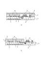
従来例として特許文献1及び2の技術について説明する。図1(a)及び図1(b)の各々は、特許文献1及び2の各々に係る電子部品モジュールの断面図である。 The techniques of
図1(a)に示すように、内導体層3を有するセラミック多層基板5の上面に設けられた電極8に、バンプ12を介してSAWデバイスチップ10が接続されている。すなわち、SAWデバイスチップ10はセラミック多層基板5の上面にフリップチップ実装されている。また、チップ部品14が電極8に半田7により接続されている。SAWデバイスチップ10及びチップ部品14は、樹脂からなる側壁4及び樹脂からなるリッド6(樹脂蓋)により封止されている。また、図1(b)に示すように、複数のSAWデバイスチップ10が個別に側壁4とリッド6とにより封止され、チップ部品14は封止されない構造を採ることもある。
しかしながら、図1(a)及び図1(b)に示した電子部品モジュールでは、側壁及びリッドが樹脂により形成されているため、気密性が劣るという課題があった。 However, in the electronic component module shown in FIGS. 1 (a) and 1 (b), the side wall and the lid are formed of resin, and thus there is a problem that the airtightness is inferior.
本発明は上記課題に鑑み、気密性が高い電子部品モジュール及びその製造方法を提供することを目的とする。 An object of this invention is to provide an electronic component module with high airtightness, and its manufacturing method in view of the said subject.
本発明は、絶縁性基板と、前記絶縁性基板の上面にフリップチップ実装されたデバイスチップと、前記絶縁性基板に接続されたチップ部品と、前記絶縁性基板と前記デバイスチップとの上に設けられたリッドと、前記絶縁性基板の上面の周辺部に、前記絶縁性基板の上面を囲むように設けられた第1金属パターンと、前記リッドの前記絶縁性基板と対向する面の周辺部に、前記リッドの前記絶縁性基板と対向する面を囲むように設けられた第2金属パターンと、前記第1金属パターンと前記第2金属パターンとを、前記絶縁性基板と前記リッドとの間であって前記第1金属パターン及び前記第2金属パターンの設けられていない領域並びに前記絶縁性基板と前記デバイスチップとの間に空洞が形成されるように接合する封止半田とを具備し、前記チップ部品は前記絶縁性基板の上面に実装され、前記第2金属パターンは前記デバイスチップと重なり、かつ前記チップ部品と重ならないように設けられ、前記封止半田は前記デバイスチップの上面を覆うように、前記第1金属パターンと前記第2金属パターンとを接合することを特徴とする電子部品モジュールである。本発明によれば、気密性が高い電子部品モジュールを提供することができる。The present invention provides an insulating substrate, a device chip flip-chip mounted on the upper surface of the insulating substrate, a chip component connected to the insulating substrate, and the insulating substrate and the device chip. A lid, a first metal pattern provided to surround the upper surface of the insulating substrate at a peripheral portion of the upper surface of the insulating substrate, and a peripheral portion of a surface of the lid facing the insulating substrate. The second metal pattern provided to surround the surface of the lid facing the insulating substrate, the first metal pattern and the second metal pattern between the insulating substrate and the lid. therecomprises a sealing solder Metropolitan joining such that a cavity is formed between the first metal pattern and the areas not provided the second metal pattern and said insulating substrate and the devicechip, The chip component is mounted on the upper surface of the insulating substrate, the second metal pattern is provided so as to overlap the device chip and not to overlap the chip component, and the sealing solder covers the upper surface of the device chip. Thus, the electronic component module is characterizedby joining the first metal pattern and the second metal pattern . ADVANTAGE OF THE INVENTION According to this invention, an electronic component module with high airtightness can be provided.
上記構成において、前記封止半田は、前記第1金属パターンと前記第2金属パターンとを接合することにより前記デバイスチップを封止し、前記デバイスチップの前記チップ部品側の面は封止されていない構成とすることができる。この構成によれば、デバイスチップとチップ部品とは絶縁されるため、独立に動作することが可能となる。In the above configuration, thesealing solder seals the device chip by bonding the first metal pattern and the second metal pattern, and the surface of the device chip on the chip component side is sealed. There can beno configuration. According to this configuration, since the device chip and the chip component are insulated, it is possible to operate independently.
本発明は、絶縁性基板と、前記絶縁性基板の上面にフリップチップ実装されたデバイスチップと、前記絶縁性基板に接続されたチップ部品と、前記絶縁性基板と前記デバイスチップとの上に設けられたリッドと、前記絶縁性基板の上面の周辺部に、前記絶縁性基板の上面を囲むように設けられた第1金属パターンと、前記リッドの前記絶縁性基板と対向する面の周辺部に、前記リッドの前記絶縁性基板と対向する面を囲むように設けられた第2金属パターンと、前記第1金属パターンと前記第2金属パターンとを、前記絶縁性基板と前記リッドとの間であって前記第1金属パターン及び前記第2金属パターンの設けられていない領域並びに前記絶縁性基板と前記デバイスチップとの間に空洞が形成されるように接合する封止半田とを具備し、前記チップ部品は前記リッドの前記絶縁性基板と対向する面とは反対の面に実装され、前記チップ部品は前記リッドに設けられたビア及び前記空洞に形成された配線を介して前記絶縁性基板と接続されている構成とすることができる。本発明によれば、電子部品モジュールの小型化が可能となる。また、デバイスチップとチップ部品とは絶縁されるため、独立に動作することが可能となる。The present invention provides an insulating substrate, a device chip flip-chip mounted on the upper surface of the insulating substrate, a chip component connected to the insulating substrate, and the insulating substrate and the device chip. A lid, a first metal pattern provided to surround the upper surface of the insulating substrate at a peripheral portion of the upper surface of the insulating substrate, and a peripheral portion of a surface of the lid facing the insulating substrate. The second metal pattern provided to surround the surface of the lid facing the insulating substrate, the first metal pattern and the second metal pattern between the insulating substrate and the lid. there comprises a sealing solder Metropolitan joining such that a cavity is formed between the first metal pattern and the areas not provided the second metal pattern and said insulating substrate and the device chip, The chip component is mounted on a surface of the lid opposite to the surface facing the insulating substrate, and the chip component is connected to the insulating substrate via vias provided in the lid and wiring formed in the cavity. It can be set as the structure connected with. According to thepresent invention , the electronic component module can be miniaturized. In addition, since the device chip and the chip component are insulated, it is possible to operate independently.
上記構成において、前記リッドにシールドパターンが設けられている構成とすることができる。この構成によれば、外部からの電気的なノイズを遮断することができる。 The said structure WHEREIN: It can be set as the structure by which the shield pattern was provided in the said lid. According to this configuration, external electrical noise can be blocked.
上記構成において、複数の前記デバイスチップがフリップチップ実装されている構成とすることができる。この構成によれば、電子部品モジュールの集積度を高めることができる。 In the above configuration, a plurality of the device chips can be flip-chip mounted. According to this configuration, the degree of integration of the electronic component module can be increased.
本発明は、絶縁性基板と、前記絶縁性基板の上面にフリップチップ実装されたデバイスチップと、前記絶縁性基板に接続されたチップ部品と、前記絶縁性基板と前記デバイスチップとの上に設けられたリッドと、前記絶縁性基板の上面の周辺部に、前記絶縁性基板の上面を囲むように設けられた第1金属パターンと、前記リッドの前記絶縁性基板と対向する面の周辺部に、前記リッドの前記絶縁性基板と対向する面を囲むように設けられた第2金属パターンと、前記第1金属パターンと前記第2金属パターンとを、前記絶縁性基板と前記リッドとの間であって前記第1金属パターン及び前記第2金属パターンの設けられていない領域並びに前記絶縁性基板と前記デバイスチップとの間に空洞が形成されるように接合する封止半田と、前記リッドの前記絶縁性基板と対向する面とは反対の面にフリップチップ実装された別のデバイスチップと、前記別のデバイスチップの上に設けられた別のリッドと、前記リッドの前記絶縁性基板と対向する面とは反対の面の周辺部に、前記絶縁性基板と対向する面とは反対の面を囲むように設けられた第3金属パターンと、前記別のリッドの前記リッドと対向する面の周辺部に、前記リッドと対向する面を囲むように設けられた第4金属パターンと、前記第3金属パターンと前記第4金属パターンとを、前記リッドと前記別のリッドとの間であって前記第3金属パターン及び前記第4金属パターンの設けられていない領域並びに前記リッドと前記別のデバイスチップとの間に空洞が形成されるように接合する別の封止半田とを具備する構成とすることができる。本発明によれば、電子部品モジュールの実装密度を高めることができる。The present invention provides an insulating substrate, a device chip flip-chip mounted on the upper surface of the insulating substrate, a chip component connected to the insulating substrate, and the insulating substrate and the device chip. A lid, a first metal pattern provided to surround the upper surface of the insulating substrate at a peripheral portion of the upper surface of the insulating substrate, and a peripheral portion of a surface of the lid facing the insulating substrate. The second metal pattern provided to surround the surface of the lid facing the insulating substrate, the first metal pattern and the second metal pattern between the insulating substrate and the lid. a sealing solder joining such that a cavity is formed between the first metal pattern and the areas not provided the second metal pattern and said insulating substrate and the device chip a, the ripple Another device chip flip-chip mounted on a surface opposite to the surface facing the insulating substrate, another lid provided on the other device chip, and the insulating substrate of the lid A third metal pattern provided on the periphery of the surface opposite to the opposing surface so as to surround the surface opposite to the surface facing the insulating substrate, and a surface facing the lid of the other lid The fourth metal pattern, the third metal pattern, and the fourth metal pattern provided on the periphery of the lid so as to surround the surface facing the lid, are disposed between the lid and the other lid. A region in which the third metal pattern and the fourth metal pattern are not provided, and another sealing solder that is joined so that a cavity is formed between the lid and the other device chip. To do Can. According to thepresent invention , the mounting density of electronic component modules can be increased.
上記構成において、前記デバイスチップは弾性波デバイスチップである構成とすることができる。 In the above configuration, the device chip may be an acoustic wave device chip.
本発明は、絶縁性基板の上面にデバイスチップをフリップチップ実装する工程と、前記絶縁性基板とチップ部品とを接続する工程と、前記絶縁性基板の上面の周辺部に前記上面を囲むように設けられた第1金属パターンと、リッドの前記絶縁性基板と対向する面に前記絶縁性基板と対向する面を囲むように設けられた第2金属パターンとを、前記絶縁性基板と前記リッドとの間であって前記第1金属パターン及び前記第2金属パターンの設けられていない領域並びに前記絶縁性基板と前記デバイスチップとの間に空洞が形成されるように封止半田で接合する工程と、を有し、前記チップ部品を接続する工程は、前記絶縁性基板の上面に前記チップ部品を実装する工程であり、前記第2金属パターンは前記デバイスチップと重なり、かつ前記チップ部品と重ならないように設けられ、前記封止半田で接合する工程は、前記デバイスチップの上面を覆うように、前記第1金属パターンと前記第2金属パターンとを接合する工程であることを特徴とする電子部品モジュールの製造方法である。本発明によれば、気密性が高い電子部品モジュールの製造方法を提供することができる。The present invention includes a step of flip-chip mounting a device chip on an upper surface of an insulating substrate, a step of connecting the insulating substrate and a chip component, and a peripheral portion of the upper surface of the insulating substrate surrounding the upper surface. A first metal pattern provided and a second metal pattern provided on a surface of the lid facing the insulating substrate so as to surround the surface facing the insulating substrate; the insulating substrate and the lid; Bonding with sealing solder so that a cavity is formed between the insulating substrate and the device chip, and a region where the first metal pattern and the second metal pattern are not provided. ,have astep of connecting the chip component is a step of mounting the chip component on the upper surface of the insulating substrate, the second metal pattern overlaps with the device chip, and the switch It provided so as not to overlap the up part, thestep of joining with the sealing solder, so as to cover the upper surface of the device chip, a step of bonding the first metal pattern and the second metal pattern It is the manufacturing method of the electronic component module characterized. ADVANTAGE OF THE INVENTION According to this invention, the manufacturing method of an electronic component module with high airtightness can be provided.
上記構成において、前記封止半田で接合する工程は、前記デバイスチップを封止するように前記第1金属パターンと前記第2金属パターンとを接合する工程であり、前記デバイスチップの前記チップ部品側の面は封止されない構成とすることができる。この構成によれば、デバイスチップとチップ部品とは絶縁されるため、独立に動作することが可能となる。In the above configuration,the step of bonding with the sealing solder is a step of bonding the first metal pattern and the second metal pattern so as to seal the device chip, and the chip component side of the device chip This surface can be configurednot to besealed . According to this configuration, since the device chip and the chip component are insulated, it is possible to operate independently.
本発明は、絶縁性基板の上面にデバイスチップをフリップチップ実装する工程と、前記絶縁性基板とチップ部品とを接続する工程と、前記絶縁性基板の上面の周辺部に前記上面を囲むように設けられた第1金属パターンと、リッドの前記絶縁性基板と対向する面に前記絶縁性基板と対向する面を囲むように設けられた第2金属パターンとを、前記絶縁性基板と前記リッドとの間であって前記第1金属パターン及び前記第2金属パターンの設けられていない領域並びに前記絶縁性基板と前記デバイスチップとの間に空洞が形成されるように封止半田で接合する工程と、を有し、前記チップ部品を接続する工程は、前記リッドの前記絶縁性基板と対向する面とは反対の面に前記チップ部品を実装し、前記リッドに設けられたビア及び前記空洞に形成された配線を介して前記基板と接続する工程である構成とすることができる。この構成によれば、電子部品モジュールの小型化が可能となる。また、デバイスチップとチップ部品とは絶縁されるため、独立に動作することが可能となる。
The present invention includes a step of flip-chip mounting a device chip on an upper surface of an insulating substrate, a step of connecting the insulating substrate and a chip component, and a peripheral portion of the upper surface of the insulating substrate surrounding the upper surface. A first metal pattern provided and a second metal pattern provided on a surface of the lid facing the insulating substrate so as to surround the surface facing the insulating substrate; the insulating substrate and the lid; Bonding with sealing solder so that a cavity is formed between the insulating substrate and the device chip, and a region where the first metal pattern and the second metal pattern are not provided. has a step of connecting the chip component, the chip component was mounted on the surface opposite to the insulating substrate and the opposing surfaces of the lid, form a via and the cavity provided on the lid And the wiring can be configured is a step of connecting to the substrate via. According to this configuration, the electronic component module can be reduced in size. In addition, since the device chip and the chip component are insulated, it is possible to operate independently.
上記構成において、前記封止半田で接合する工程は、前記絶縁性基板と前記リッドとの間に半田シートを配置し、前記半田シートを加熱及び加圧する工程である構成とすることができる。この構成によれば、半田シートが溶融し、第1金属パターン及び第2金属パターンに沿って流動するため、電子部品モジュールを気密性高く封止することができる。また、一度の工程で配線と封止半田とを形成することができる。 The said structure WHEREIN: The process joined by the said sealing solder can be set as the structure which is a process which arrange | positions a solder sheet between the said insulating substrate and the said lid, and heats and pressurizes the said solder sheet. According to this configuration, since the solder sheet melts and flows along the first metal pattern and the second metal pattern, the electronic component module can be sealed with high airtightness. Further, the wiring and the sealing solder can be formed in a single process.
本発明によれば、気密性が高い電子部品モジュール及びその製造方法を提供することができる。 ADVANTAGE OF THE INVENTION According to this invention, an electronic component module with high airtightness and its manufacturing method can be provided.
図面を用いて、本発明の実施例について説明する。 Embodiments of the present invention will be described with reference to the drawings.
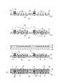
図2(a)は実施例1に係る電子部品モジュールの断面図であり、図2(b)は基板の上面図、図2(c)はリッドの下面図である。図の簡略化のため、縮尺については省略して図示している。 2A is a cross-sectional view of the electronic component module according to the first embodiment, FIG. 2B is a top view of the substrate, and FIG. 2C is a bottom view of the lid. In order to simplify the drawing, the scale is not shown.
図2(a)に示すように、例えばアルミナを主成分とする高温焼成セラミック(HTCC)等の絶縁体からなる、厚さT1が例えば0.2mmの絶縁性基板2の上面に、例えばAlからなる電極8が設けられている。二つのSAWデバイスチップ10は、例えばAu等の金属からなるバンプ12を介して電極8に接続されている。すなわち、SAWデバイスチップ10は絶縁性基板2の上面にフリップチップ実装されている。SAWデバイスチップ10の高さH1は例えば0.2〜0.3mmである。チップ部品14と電極8とは、例えばSn−Ag等からなる半田7を用いて接続されている。すなわち、チップ部品14は絶縁性基板2の上面に実装されている。チップ部品の高さH2は例えば0.2〜0.3mmである。電極8は絶縁性基板2の下面に設けられた例えばW+Ni+Au等の金属からなる端子18と導通している。絶縁性基板2、SAWデバイスチップ10及びチップ部品14の上には、例えばアルミナを主成分とする高温焼成セラミック等の絶縁体からなる、厚さT2が例えば0.2〜0.4mmのリッド16が設けられている。 As shown in FIG. 2A, an upper surface of an insulating
図2(b)及び図2(a)に示すように、絶縁性基板2の上面の周辺部には、上面を囲むように、例えばAu等の金属からなる、例えば厚さT3が1〜30μmの第1金属パターン22が設けられている。 As shown in FIGS. 2B and 2A, the peripheral portion of the upper surface of the insulating
図2(c)及び図2(a)に示すように、リッド16の絶縁性基板2と対向する面(下面)には、下面を囲み、かつSAWデバイスチップ10と重なるように例えばAu等の金属からなる、例えば厚さT4が1〜30μmの第2金属パターン24が設けられている。また、チップ部品14と重なる部分には第2金属パターン24は設けられていない。SAWデバイスチップ10の上面と第2金属パターン24との間の高さH3は例えば0.1mm以下である。 2C and 2A, the surface (lower surface) of the
図2(a)に示すように、第1金属パターン22と第2金属パターン24とは、例えばSn−Agからなる封止半田20により接合されている。すなわち、SAWデバイスチップ10とチップ部品14とはリッド16と封止半田20とにより封止されている。このとき、絶縁性基板2とSAWデバイスチップ10との間、及び絶縁性基板2とリッド16との間であって第1金属パターン22及び第2金属パターン24が設けられていない領域に空洞28が形成される。すなわち、チップ部品14とSAWデバイスチップ10との間、チップ部品14と封止半田20との間に空洞28が形成される。 As shown in FIG. 2A, the
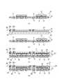
次に、実施例1に係る電子部品モジュールの製造方法について説明する。図3(a)から図4(b)は実施例1に係る電子部品モジュールの製造方法を示す断面図である。 Next, a method for manufacturing the electronic component module according to the first embodiment will be described. FIG. 3A to FIG. 4B are cross-sectional views illustrating the method for manufacturing the electronic component module according to the first embodiment.
図3(a)に示すように、多面取り構造の絶縁性基板32の上面に設けられた電極8に半田7を印刷し、チップ部品14を接続する。すなわち、表面実装技術を用いて、チップ部品14を絶縁性基板32の上面に実装する。 As shown in FIG. 3A,
図3(b)に示すように、バンプ12を用いてSAWデバイスチップ10を絶縁性基板32の上面にフリップチップ実装する。 As shown in FIG. 3B, the
図3(c)に示すように、絶縁性基板32、SAWデバイスチップ10及びチップ部品14の上に半田シート35及びリッド34を配置する。このとき、絶縁性基板32とリッド34との間に半田シート35が配置される。 As shown in FIG. 3C, the
図3(d)に示すように、半田シート35を加熱及び加圧することで、溶融した半田シート35は絶縁性基板32の上面に設けられた第1金属パターン22及びリッド34の下面に設けられた第2金属パターン24に沿って流動する。溶融した半田が固化することで、第1金属パターン22と第2金属パターン24とは封止半田20で接合される。すなわち、SAWデバイスチップ10とチップ部品14とがリッド16と封止半田20とにより封止される。このとき、絶縁性基板32とリッド16との間であって第1金属パターン22及び第2金属パターン24が設けられていない領域、並びに絶縁性基板32とSAWデバイスチップ10との間には空洞28が形成される。 As shown in FIG. 3D, the
図4(a)に示すように、例えばダイシング工程を行うことにより、リッド16及び封止半田20を切断する。このとき、絶縁性基板32は切断されない。 As shown in FIG. 4A, the
図4(b)に示すように、無電解メッキ法または電解メッキ法により、例えばNi等のからなる金属膜26を封止半田20の表面に形成する。この後、絶縁性基板32を切断することにより図2(a)に示した電子部品モジュールが完成する。 As shown in FIG. 4B, a
実施例1によれば、溶融した半田が第1金属パターン22と第2金属パターン24とに沿って流動し、両者を接合するため、樹脂で封止する場合よりも気密性の高い電子部品モジュールを提供することができる。これにより、耐湿性はMSL1を維持することができた。 According to the first embodiment, the molten solder flows along the
図2(a)に示すように、チップ部品14とSAWデバイスチップ10との間、チップ部品14と封止半田20との間に空洞28が形成される。すなわち、チップ部品14と封止半田20とは絶縁される。同様に、SAWデバイスチップ10と封止半田20とは絶縁される。従って、SAWデバイスチップ10とチップ部品14とは、各々が独立に動作することが可能となる。これを用いて、例えばチップ部品14を整合回路とし、SAWデバイスチップ10と組み合わせて実装することで、安価な高温焼成セラミックからなる絶縁性基板2を用いて、低コストかつ気密性の高いデュプレクサを提供することができる。 As shown in FIG. 2A,
第2金属パターン24はリッド16の下面を囲むように設けられていれば、封止半田20で封止することができる。しかし、第2金属パターン24がSAWデバイスチップ10と重なる位置に設けられているため、封止半田20はSAWデバイスチップ10の上面を覆うこととなる。これにより、第2金属パターン24と封止半田20とは外部からの電気的なノイズを遮断するシールドとして機能する。また、封止半田20がSAWデバイスチップ10を上から押さえつけるため、絶縁性基板2とSAWデバイスチップ10との接合強度が向上する。従って、第2金属パターン24はSAWデバイスチップ10と重なる位置に設けられていることが好ましい。 If the
バンプ12はAuに限定されないが、図3(b)から図3(d)に示すように、SAWデバイスチップ10のフリップチップ実装工程の後に半田シート35を加熱する封止工程を行うため、バンプ12を形成する金属は、半田シート35を形成する半田の融点よりも高いことが好ましい。また、第1金属パターン22及び第2金属パターン24もAuに限定されず、封止半田20との濡れ性が良好な金属であればよい。 The
金属膜26は形成されなくてもよいが、機械的強度を向上させるためには金属膜26が形成されていることが好ましい。 The
実施例2は、リッド16にシールドパターンが設けられている例である。図5(a)及び図5(b)は実施例2に係る電子部品モジュールの断面図である。既述した構成と同様の構成については説明を省略する。 The second embodiment is an example in which a shield pattern is provided on the
図5(a)に示すように、リッド16の上面に例えばW+Ni+Au等の金属からなるシールドパターン30が設けられており、その上にはメッキにより形成された金属膜26が設けられている。 As shown in FIG. 5A, a
また、図5(b)に示すように、リッド16がいずれも例えば高温焼成セラミックからなる複数の層16a及び16bを有し、その間にシールドパターン30が設けられていてもよい。 Further, as shown in FIG. 5B, the
実施例2によれば、シールドパターン30が設けられているため、電気的なノイズを遮断する効果をより大きくすることができる。 According to the second embodiment, since the
実施例3はリッドの上面にチップ部品が実装されている例である。図6(a)は実施例3に係る電子部品モジュールの断面図であり、図6(b)から図6(d)の各々は、絶縁性基板の上面図、リッドの下面図、リッドの上面図である。 The third embodiment is an example in which a chip component is mounted on the upper surface of the lid. FIG. 6A is a cross-sectional view of the electronic component module according to the third embodiment. Each of FIGS. 6B to 6D includes a top view of an insulating substrate, a bottom view of the lid, and a top view of the lid. FIG.
図6(a)及び図6(d)に示すように、リッド16の絶縁性基板2と対向する面とは反対の面(上面)に設けられた例えばW+Ni+Au等の金属からなる電極36a及び36bにチップ部品14が、半田7を用いて接続されている。すなわち、チップ部品14がリッド16の上面に実装されている。 As shown in FIGS. 6A and 6D,
図6(b)に示すように、絶縁性基板2の上面には電極9が設けられている。電極38と電極9とは、例えばW+Ni+Au等の金属からなる。また、図6(c)に示すように、リッド16の下面には、第2金属パターン24と絶縁されている電極38が設けられている。 As shown in FIG. 6B, an
リッド16の上面に設けられた電極36aと、下面に設けられた電極38とは、直径R1が例えば0.3mmで、リッド16を貫通し、内部に例えばWやCu等の金属が充填されたビア40を介して接続されている。また、電極36aと電極9とは、空洞28に形成された、直径R2がR1より大きく、例えばSn−Ag等の半田からなる配線42により接続されている。すなわち、チップ部品14と絶縁性基板2とは接続されている。また、電極36bと第2金属パターン24とはビア40を介して接続されている。すなわち、電極36bは接地されている。 The
図7(a)から図8(b)は、実施例3に係る電子部品モジュールの製造方法を示す断面図である。 FIG. 7A to FIG. 8B are cross-sectional views illustrating a method for manufacturing an electronic component module according to the third embodiment.
図7(a)に示すように、絶縁性基板32の上面にSAWデバイスチップ10をフリップチップ実装する。 As shown in FIG. 7A, the
図7(b)に示すように、絶縁性基板32及びSAWデバイスチップの上に半田シート35とリッド34とを配置する。 As shown in FIG. 7B, a
図7(c)に示すように、半田シート35を加熱及び加圧することで、第1金属パターン22と第2金属パターン24とが接合される。このとき、図3(d)と同様に、絶縁性基板32とリッド16との間であって第1金属パターン22及び第2金属パターン24が設けられていない領域、並びに絶縁性基板32とSAWデバイスチップ10との間には空洞28が形成される。また、空洞28には、電極38と電極9とを接続する配線42が形成される。 As shown in FIG. 7C, the
図7(d)に示すように、例えばダイシング工程を行うことにより、リッド16及び封止半田20を切断する。 As shown in FIG. 7D, the
図8(a)に示すように、無電解メッキ法または電解メッキ法により、例えばNi等の金属からなる金属膜26を封止半田20の表面に形成する。 As shown in FIG. 8A, a
図8(b)に示すように、リッド16の上面に半田7を印刷し、チップ部品14を電極36a及び36bに接続する。すなわち、表面実装技術を用いて、チップ部品14をリッド16の上面に実装する。この後、絶縁性基板32を切断することにより、実施例3に係る電子部品モジュールが完成する。 As shown in FIG. 8B,
実施例3によれば、絶縁性基板2にチップ部品14を実装するスペースを設けなくてよいため、電子部品モジュールの面積を縮小することが可能となる。また、配線42は空洞28に形成されるため、封止半田20及びSAWデバイスチップ10と絶縁される。従って、SAWデバイスチップ10とチップ部品14とは絶縁され、各々が独立に動作することが可能となる。これにより、小型化可能で、かつ気密性が高い電子部品モジュールを提供することができる。また、図7(d)に示すように、配線42と封止半田20とは、一度の工程で半田シート35から形成することができる。すなわち、工程を簡略化することができる。 According to the third embodiment, since it is not necessary to provide a space for mounting the
図9は実施例3の変形例に係る電子部品モジュールの断面図である。図9に示すように、チップ部品14が例えばエポキシ等からなる樹脂44により封止されている。これにより、リッド16の上面に実装されたチップ部品14を保護することができる。 FIG. 9 is a cross-sectional view of an electronic component module according to a modification of the third embodiment. As shown in FIG. 9, the
実施例4は、電子部品モジュールの実装密度を高めた例である。図10(a)及び図10(b)は実施例4に係る電子部品モジュールの断面図である。 Example 4 is an example in which the mounting density of the electronic component module is increased. 10A and 10B are cross-sectional views of the electronic component module according to the fourth embodiment.
図10(a)に示すように、リッド16の上面に設けられた電極36に二つのSAWデバイスチップ50(別のデバイスチップ)がバンプ12を介して接続されている。すなわちSAWデバイスチップ50はリッド16の上面にフリップチップ実装されている。リッド16の上面の周辺部には、上面を囲むように第3金属パターン54が設けられている。また、リッド16の上に設けられたリッド46(別のリッド)の下面の周辺部には、下面を囲みかつSAWデバイスチップ50に重なるように第4金属パターン56が設けられている。第3金属パターン54と第4金属パターン56とは、第1金属パターン22等と同様に、例えばAu等の金属からなる。封止半田21(別の封止半田)は第3金属パターン54と第4金属パターン56を接合している。すなわち、チップ部品14とSAWデバイスチップ50とはリッド46と封止半田21とにより封止されている。このとき、リッド16とリッド46との間であって第3金属パターン54及び第4金属パターンが設けられていない領域、並びにリッド16とSAWデバイスチップ50との間に空洞58が形成される。第3金属パターン54と第2金属パターン24、電極36bと電極38とは各々ビア40を介して接続されている。 As shown in FIG. 10A, two SAW device chips 50 (another device chip) are connected to the
リッド46の上面に設けられた、電極59a及び59bに、チップ部品14が半田7を介して接続されている。すなわち、チップ部品14はリッド46の上面に実装されている。電極59aとリッド46の下面に設けられた電極57とはビア48を介して接続されている。また、電極57とリッド16の上面に設けられた電極53とは、空洞58に形成された配線52を介して接続されている。すなわち、チップ部品14はリッド16と接続されている。また、電極59bと第4金属パターン56とはビア40を介して接続されている。すなわち、電極59bは接地されている。 The
また、図10(b)に示すように、リッド16の上面にチップ部品14を実装せず、リッド16の上面にのみチップ部品14が実装されている構成としてもよい。 Further, as shown in FIG. 10B, the
実施例4によれば、リッド16の上面にチップ部品14及びSAWデバイスチップ50を実装し、封止半田21とリッド46とで封止することができる。また、配線52は空洞58に設けられている。すなわち、二つのチップ部品14の各々とSAWデバイスチップ50とは絶縁されるため、各々独立して動作することが可能となる。これにより、実装密度が高く、かつ気密性が高い電子部品モジュールを提供することができる。 According to the fourth embodiment, the
実施例においては、二つのSAWデバイスチップを実装する例を示したが、一つ、または三つ以上でもよい。複数のSAWデバイスチップを実装することで、集積度を高めることができる。また、SAWデバイスチップ以外の弾性波デバイスチップ、または弾性波デバイスチップ以外のデバイスチップ、例えばスイッチやアンプ等でもよい。 In the embodiment, an example in which two SAW device chips are mounted has been described, but one or three or more may be used. The degree of integration can be increased by mounting a plurality of SAW device chips. Also, an acoustic wave device chip other than the SAW device chip, or a device chip other than the acoustic wave device chip, such as a switch or an amplifier, may be used.
以上、本発明の実施例について詳述したが、本発明は係る特定の実施例に限定されるものではなく、特許請求の範囲に記載された本発明の要旨の範囲内において、種々の変形・変更が可能である。 Although the embodiments of the present invention have been described in detail above, the present invention is not limited to such specific embodiments, and various modifications and changes can be made within the scope of the gist of the present invention described in the claims. It can be changed.
絶縁性基板 2、32
リッド 6、16、34、46
SAWデバイスチップ 10、50
チップ部品 14
封止半田 20、21
第1金属パターン 22
第2金属パターン 24
ビア 40、48
配線 42、52
第3金属パターン 54
第4金属パターン 56Insulating
Sealing
Via 40, 48
Claims (11)
Translated fromJapanese前記絶縁性基板の上面にフリップチップ実装されたデバイスチップと、
前記絶縁性基板に接続されたチップ部品と、
前記絶縁性基板と前記デバイスチップとの上に設けられたリッドと、
前記絶縁性基板の上面の周辺部に、前記絶縁性基板の上面を囲むように設けられた第1金属パターンと、
前記リッドの前記絶縁性基板と対向する面の周辺部に、前記リッドの前記絶縁性基板と対向する面を囲むように設けられた第2金属パターンと、
前記第1金属パターンと前記第2金属パターンとを、前記絶縁性基板と前記リッドとの間であって前記第1金属パターン及び前記第2金属パターンの設けられていない領域並びに前記絶縁性基板と前記デバイスチップとの間に空洞が形成されるように接合する封止半田とを具備し、
前記チップ部品は前記絶縁性基板の上面に実装され、
前記第2金属パターンは前記デバイスチップと重なり、かつ前記チップ部品と重ならないように設けられ、前記封止半田は前記デバイスチップの上面を覆うように、前記第1金属パターンと前記第2金属パターンとを接合することを特徴とする電子部品モジュール。An insulating substrate;
A device chip flip-chip mounted on the upper surface of the insulating substrate;
A chip component connected to the insulating substrate;
A lid provided on the insulating substrate and the device chip;
A first metal pattern provided on the periphery of the upper surface of the insulating substrate so as to surround the upper surface of the insulating substrate;
A second metal pattern provided around a surface of the lid facing the insulating substrate so as to surround the surface of the lid facing the insulating substrate;
The first metal pattern and the second metal pattern, the region between the insulating substrate and the lid, where the first metal pattern and the second metal pattern are not provided, and the insulating substrate;comprising a sealing solder Metropolitan joining such that a cavity is formed between the devicechip,
The chip component is mounted on the upper surface of the insulating substrate,
The second metal pattern is provided so as to overlap the device chip and not to overlap the chip component, and the sealing solder covers the upper surface of the device chip so that the first metal pattern and the second metal pattern are covered. And an electronic component module.
前記デバイスチップの前記チップ部品側の面は封止されていないことを特徴とする請求項1記載の電子部品モジュール。The sealing solder seals the device chip by bonding the first metal pattern and the second metal pattern,
2. The electronic component module according to claim 1, wherein a surface of the device chip on the chip component side is not sealed .
前記絶縁性基板の上面にフリップチップ実装されたデバイスチップと、
前記絶縁性基板に接続されたチップ部品と、
前記絶縁性基板と前記デバイスチップとの上に設けられたリッドと、
前記絶縁性基板の上面の周辺部に、前記絶縁性基板の上面を囲むように設けられた第1金属パターンと、
前記リッドの前記絶縁性基板と対向する面の周辺部に、前記リッドの前記絶縁性基板と対向する面を囲むように設けられた第2金属パターンと、
前記第1金属パターンと前記第2金属パターンとを、前記絶縁性基板と前記リッドとの間であって前記第1金属パターン及び前記第2金属パターンの設けられていない領域並びに前記絶縁性基板と前記デバイスチップとの間に空洞が形成されるように接合する封止半田とを具備し、
前記チップ部品は前記リッドの前記絶縁性基板と対向する面とは反対の面に実装され、前記チップ部品は前記リッドに設けられたビア及び前記空洞に形成された配線を介して前記絶縁性基板と接続されていることを特徴とする電子部品モジュール。An insulating substrate;
A device chip flip-chip mounted on the upper surface of the insulating substrate;
A chip component connected to the insulating substrate;
A lid provided on the insulating substrate and the device chip;
A first metal pattern provided on the periphery of the upper surface of the insulating substrate so as to surround the upper surface of the insulating substrate;
A second metal pattern provided around a surface of the lid facing the insulating substrate so as to surround the surface of the lid facing the insulating substrate;
The first metal pattern and the second metal pattern, the region between the insulating substrate and the lid, where the first metal pattern and the second metal pattern are not provided, and the insulating substrate; A sealing solder that is joined so that a cavity is formed between the device chip and
The chip component is mounted on a surface of the lid opposite to the surface facing the insulating substrate, and the chip component is connected to the insulating substrate via vias provided in the lid and wiring formed in the cavity.An electronic component modulecharacterized by being connected to.
前記絶縁性基板の上面にフリップチップ実装されたデバイスチップと、
前記絶縁性基板に接続されたチップ部品と、
前記絶縁性基板と前記デバイスチップとの上に設けられたリッドと、
前記絶縁性基板の上面の周辺部に、前記絶縁性基板の上面を囲むように設けられた第1金属パターンと、
前記リッドの前記絶縁性基板と対向する面の周辺部に、前記リッドの前記絶縁性基板と対向する面を囲むように設けられた第2金属パターンと、
前記第1金属パターンと前記第2金属パターンとを、前記絶縁性基板と前記リッドとの間であって前記第1金属パターン及び前記第2金属パターンの設けられていない領域並びに前記絶縁性基板と前記デバイスチップとの間に空洞が形成されるように接合する封止半田と、
前記リッドの前記絶縁性基板と対向する面とは反対の面にフリップチップ実装された別のデバイスチップと、
前記別のデバイスチップの上に設けられた別のリッドと、
前記リッドの前記絶縁性基板と対向する面とは反対の面の周辺部に、前記絶縁性基板と対向する面とは反対の面を囲むように設けられた第3金属パターンと、
前記別のリッドの前記リッドと対向する面の周辺部に、前記リッドと対向する面を囲むように設けられた第4金属パターンと、
前記第3金属パターンと前記第4金属パターンとを、前記リッドと前記別のリッドとの間であって前記第3金属パターン及び前記第4金属パターンの設けられていない領域並びに前記リッドと前記別のデバイスチップとの間に空洞が形成されるように接合する別の封止半田とを具備することを特徴とする電子部品モジュール。An insulating substrate;
A device chip flip-chip mounted on the upper surface of the insulating substrate;
A chip component connected to the insulating substrate;
A lid provided on the insulating substrate and the device chip;
A first metal pattern provided on the periphery of the upper surface of the insulating substrate so as to surround the upper surface of the insulating substrate;
A second metal pattern provided around a surface of the lid facing the insulating substrate so as to surround the surface of the lid facing the insulating substrate;
The first metal pattern and the second metal pattern, the region between the insulating substrate and the lid, where the first metal pattern and the second metal pattern are not provided, and the insulating substrate; Sealing solder that is joined so that a cavity is formed between the device chip,
Another device chip flip-chip mounted on the surface of the lid opposite to the surface facing the insulating substrate;
Another lid provided on the other device chip;
A third metal pattern provided on the periphery of the surface opposite to the surface facing the insulating substrate of the lid so as to surround the surface opposite to the surface facing the insulating substrate;
A fourth metal pattern provided on the periphery of the surface facing the lid of the other lid so as to surround the surface facing the lid;
The third metal pattern and the fourth metal pattern are arranged between the lid and the another lid, and the region where the third metal pattern and the fourth metal pattern are not provided, and the lid and the separateAn electronic component module comprising: another sealing solder that is joined so as to form a cavity with the device chip.
前記絶縁性基板とチップ部品とを接続する工程と、
前記絶縁性基板の上面の周辺部に前記上面を囲むように設けられた第1金属パターンと、リッドの前記絶縁性基板と対向する面に前記絶縁性基板と対向する面を囲むように設けられた第2金属パターンとを、前記絶縁性基板と前記リッドとの間であって前記第1金属パターン及び前記第2金属パターンの設けられていない領域並びに前記絶縁性基板と前記デバイスチップとの間に空洞が形成されるように封止半田で接合する工程と、を有し、
前記チップ部品を接続する工程は、前記絶縁性基板の上面に前記チップ部品を実装する工程であり、
前記第2金属パターンは前記デバイスチップと重なり、かつ前記チップ部品と重ならないように設けられ、
前記封止半田で接合する工程は、前記デバイスチップの上面を覆うように、前記第1金属パターンと前記第2金属パターンとを接合する工程であることを特徴とする電子部品モジュールの製造方法。Flip chip mounting the device chip on the top surface of the insulating substrate;
Connecting the insulating substrate and the chip component;
A first metal pattern provided on the periphery of the upper surface of the insulating substrate so as to surround the upper surface; and a surface of the lid facing the insulating substrate so as to surround a surface facing the insulating substrate. A second metal pattern between the insulating substrate and the lid, where the first metal pattern and the second metal pattern are not provided, and between the insulating substrate and the device chip. and bonding a sealing solder such that a cavity is formed, apossess the,
The step of connecting the chip components is a step of mounting the chip components on the upper surface of the insulating substrate,
The second metal pattern is provided so as to overlap the device chip and not to overlap the chip component;
The step of bonding with the sealing solder is a step of bonding the first metal pattern and the second metal pattern so as to cover the upper surface of the device chip .
前記デバイスチップの前記チップ部品側の面は封止されないことを特徴とする請求項8記載の電子部品モジュールの製造方法。The step of bonding with the sealing solder is a step of bonding the first metal pattern and the second metal pattern so as to seal the device chip,
9. The method of manufacturing an electronic component module according to claim8, wherein a surface of the device chip on the chip component side is not sealed .
前記絶縁性基板とチップ部品とを接続する工程と、
前記絶縁性基板の上面の周辺部に前記上面を囲むように設けられた第1金属パターンと、リッドの前記絶縁性基板と対向する面に前記絶縁性基板と対向する面を囲むように設けられた第2金属パターンとを、前記絶縁性基板と前記リッドとの間であって前記第1金属パターン及び前記第2金属パターンの設けられていない領域並びに前記絶縁性基板と前記デバイスチップとの間に空洞が形成されるように封止半田で接合する工程と、を有し、
前記チップ部品を接続する工程は、前記リッドの前記絶縁性基板と対向する面とは反対の面に前記チップ部品を実装し、前記リッドに設けられたビア及び前記空洞に形成された配線を介して前記基板と接続する工程であることを特徴とする電子部品モジュールの製造方法。Flip chip mounting the device chip on the top surface of the insulating substrate;
Connecting the insulating substrate and the chip component;
A first metal pattern provided to surround the upper surface at a peripheral portion of the upper surface of the insulating substrate, and a surface of the lid facing the insulating substrate so as to surround the surface facing the insulating substrate. The second metal pattern is a region between the insulating substrate and the lid, where the first metal pattern and the second metal pattern are not provided, and between the insulating substrate and the device chip. Bonding with sealing solder so that a cavity is formed in
The step of connecting the chip components includes mounting the chip components on a surface of the lid opposite to the surface facing the insulating substrate, and via vias provided in the lid and wiring formed in the cavity. The method for manufacturingan electronic component module is a step of connecting to the substrate.
Priority Applications (2)
| Application Number | Priority Date | Filing Date | Title |
|---|---|---|---|
| JP2008208373AJP4555369B2 (en) | 2008-08-13 | 2008-08-13 | Electronic component module and manufacturing method thereof |
| US12/540,721US8363422B2 (en) | 2008-08-13 | 2009-08-13 | Electronic component module and method for manufacturing the same |
Applications Claiming Priority (1)
| Application Number | Priority Date | Filing Date | Title |
|---|---|---|---|
| JP2008208373AJP4555369B2 (en) | 2008-08-13 | 2008-08-13 | Electronic component module and manufacturing method thereof |
Publications (2)
| Publication Number | Publication Date |
|---|---|
| JP2010045201A JP2010045201A (en) | 2010-02-25 |
| JP4555369B2true JP4555369B2 (en) | 2010-09-29 |
Family
ID=41680490
Family Applications (1)
| Application Number | Title | Priority Date | Filing Date |
|---|---|---|---|
| JP2008208373AExpired - Fee RelatedJP4555369B2 (en) | 2008-08-13 | 2008-08-13 | Electronic component module and manufacturing method thereof |
Country Status (2)
| Country | Link |
|---|---|
| US (1) | US8363422B2 (en) |
| JP (1) | JP4555369B2 (en) |
Families Citing this family (9)
| Publication number | Priority date | Publication date | Assignee | Title |
|---|---|---|---|---|
| JP5807413B2 (en)* | 2011-07-04 | 2015-11-10 | セイコーエプソン株式会社 | Electronic device package, electronic device and electronic equipment |
| CN103249273B (en)* | 2012-02-08 | 2016-04-13 | 环旭电子股份有限公司 | Stack board structure |
| WO2014020787A1 (en) | 2012-08-03 | 2014-02-06 | パナソニック株式会社 | Electronic component module and mounting body therefor |
| JP6336714B2 (en)* | 2013-05-27 | 2018-06-06 | 富士通コンポーネント株式会社 | Electronic equipment |
| US9363892B2 (en)* | 2013-07-19 | 2016-06-07 | Google Technology Holdings LLC | Circuit assembly and corresponding methods |
| JP6315650B2 (en)* | 2013-07-31 | 2018-04-25 | 太陽誘電株式会社 | Electronic devices |
| JP6360678B2 (en)* | 2013-12-09 | 2018-07-18 | 太陽誘電株式会社 | Module and manufacturing method thereof |
| JP6284811B2 (en)* | 2014-04-14 | 2018-02-28 | 太陽誘電株式会社 | Electronic device and manufacturing method thereof |
| CN113035788B (en)* | 2019-12-25 | 2025-03-14 | 台湾积体电路制造股份有限公司 | Packaging structure and manufacturing method thereof |
Family Cites Families (26)
| Publication number | Priority date | Publication date | Assignee | Title |
|---|---|---|---|---|
| JPS6187396A (en)* | 1984-10-05 | 1986-05-02 | 株式会社日立製作所 | Electronic circuit device and its manufacturing method |
| JPH0382144A (en)* | 1989-08-25 | 1991-04-08 | Hitachi Ltd | Sealing structure of semiconductor devices |
| JPH03142860A (en)* | 1989-10-30 | 1991-06-18 | Hitachi Ltd | Method for manufacturing semiconductor integrated circuit device |
| FR2674078B1 (en)* | 1991-03-12 | 1994-10-07 | Thomson Trt Defense | MICROWAVE TRANSCEIVER USING MULTI-LAYER PRINTED CIRCUIT TECHNIQUE. |
| JPH05206313A (en)* | 1992-01-29 | 1993-08-13 | Hitachi Ltd | Semiconductor integrated circuit device and manufacturing method thereof |
| JPH06291207A (en)* | 1993-03-31 | 1994-10-18 | Toshiba Lighting & Technol Corp | Hybrid module and manufacturing method thereof |
| JPH08141745A (en)* | 1994-11-22 | 1996-06-04 | Nippon Avionics Co Ltd | IC airtight sealing method |
| JPH09130009A (en)* | 1995-10-27 | 1997-05-16 | Mitsubishi Electric Corp | Hybrid integrated circuit device and manufacturing method thereof |
| JP3042431B2 (en)* | 1996-12-03 | 2000-05-15 | 株式会社村田製作所 | Electronic component sealing structure and sealing method |
| US5990418A (en)* | 1997-07-29 | 1999-11-23 | International Business Machines Corporation | Hermetic CBGA/CCGA structure with thermal paste cooling |
| JP3598874B2 (en)* | 1998-05-27 | 2004-12-08 | 株式会社村田製作所 | Piezoelectric ceramic composition and piezoelectric element using this piezoelectric ceramic composition |
| US6137693A (en)* | 1998-07-31 | 2000-10-24 | Agilent Technologies Inc. | High-frequency electronic package with arbitrarily-shaped interconnects and integral shielding |
| JP2001267473A (en)* | 2000-03-17 | 2001-09-28 | Hitachi Ltd | Semiconductor device and method of manufacturing the same |
| JP4049239B2 (en) | 2000-08-30 | 2008-02-20 | Tdk株式会社 | Method for manufacturing high-frequency module component including surface acoustic wave element |
| JP3722209B2 (en)* | 2000-09-05 | 2005-11-30 | セイコーエプソン株式会社 | Semiconductor device |
| JP4137356B2 (en)* | 2000-09-07 | 2008-08-20 | Tdk株式会社 | Method for manufacturing high-frequency module component including surface acoustic wave element |
| JP3960156B2 (en)* | 2002-07-19 | 2007-08-15 | 千住金属工業株式会社 | Method for manufacturing lid for sealing plate-like substrate |
| JP2004364041A (en)* | 2003-06-05 | 2004-12-24 | Fujitsu Media Device Kk | Surface acoustic wave device and manufacturing method thereof |
| US7608789B2 (en)* | 2004-08-12 | 2009-10-27 | Epcos Ag | Component arrangement provided with a carrier substrate |
| JP4677991B2 (en)* | 2004-12-02 | 2011-04-27 | 株式会社村田製作所 | Electronic component and manufacturing method thereof |
| JP4456503B2 (en)* | 2004-12-24 | 2010-04-28 | 富士通メディアデバイス株式会社 | Manufacturing method of electronic parts |
| US7643311B2 (en)* | 2005-04-21 | 2010-01-05 | Stmicroelectronics Sa | Electronic circuit protection device |
| DE602006006106D1 (en)* | 2005-04-21 | 2009-05-20 | St Microelectronics Sa | Device for protecting an electrical circuit |
| JP5087335B2 (en)* | 2007-07-19 | 2012-12-05 | 日本電波工業株式会社 | Crystal oscillator for surface mounting |
| US7989928B2 (en)* | 2008-02-05 | 2011-08-02 | Advanced Semiconductor Engineering Inc. | Semiconductor device packages with electromagnetic interference shielding |
| JP2009194725A (en)* | 2008-02-15 | 2009-08-27 | Nippon Dempa Kogyo Co Ltd | Crystal oscillator for surface mounting |
- 2008
- 2008-08-13JPJP2008208373Apatent/JP4555369B2/ennot_activeExpired - Fee Related
- 2009
- 2009-08-13USUS12/540,721patent/US8363422B2/ennot_activeExpired - Fee Related
Also Published As
| Publication number | Publication date |
|---|---|
| US20100038122A1 (en) | 2010-02-18 |
| US8363422B2 (en) | 2013-01-29 |
| JP2010045201A (en) | 2010-02-25 |
Similar Documents
| Publication | Publication Date | Title |
|---|---|---|
| JP4555369B2 (en) | Electronic component module and manufacturing method thereof | |
| JP6096812B2 (en) | Electronic device mounting package, electronic device and imaging module | |
| JP6496865B2 (en) | Electronic component storage package, electronic device and electronic module | |
| KR20060073453A (en) | Electronic component and its manufacturing method | |
| JP5206377B2 (en) | Electronic component module | |
| JP4741621B2 (en) | Electronic component sealing substrate, electronic device using the same, and electronic device manufacturing method | |
| JP2018032704A (en) | Electronic device mounting substrate, electronic device and electronic module | |
| JPWO2008066087A1 (en) | MICROSTRUCTURE DEVICE, ITS MANUFACTURING METHOD, AND SEALING SUBSTRATE | |
| JP4268480B2 (en) | Electronic component sealing substrate and electronic device using the same | |
| JP6360678B2 (en) | Module and manufacturing method thereof | |
| JP4859811B2 (en) | Electronic component storage package | |
| JP7163409B2 (en) | Substrate for mounting electronic device and electronic device | |
| JP2005262382A (en) | Electronic device and manufacturing method thereof | |
| JP4126459B2 (en) | Electronic component sealing substrate, electronic device using the same, and electronic device manufacturing method | |
| JP2005212017A (en) | Electronic component sealing substrate, multi-component electronic component sealing substrate, and method of manufacturing electronic device | |
| JP2020035898A (en) | Electronic element mounting substrate, electronic device, and electronic module | |
| JP2019009375A (en) | Electronic device mounting substrate, electronic device and electronic module | |
| JP5213663B2 (en) | Electronic device mounting structure | |
| JP2017059814A (en) | Electronic component storage package and electronic device | |
| JP2011097247A (en) | High frequency module and method for manufacturing the same | |
| JP4116954B2 (en) | Electronic component sealing substrate and electronic device using the same | |
| JP6622583B2 (en) | Wiring board and electronic device | |
| JP2005212016A (en) | Electronic component sealing substrate, multi-component electronic component sealing substrate, and method of manufacturing electronic device | |
| JP2010212379A (en) | Electronic component module, and method of manufacturing the same | |
| JP2020102584A (en) | Circuit board and electronic component |
Legal Events
| Date | Code | Title | Description |
|---|---|---|---|
| A977 | Report on retrieval | Free format text:JAPANESE INTERMEDIATE CODE: A971007 Effective date:20100506 | |
| A131 | Notification of reasons for refusal | Free format text:JAPANESE INTERMEDIATE CODE: A131 Effective date:20100511 | |
| A521 | Request for written amendment filed | Free format text:JAPANESE INTERMEDIATE CODE: A523 Effective date:20100621 | |
| TRDD | Decision of grant or rejection written | ||
| A01 | Written decision to grant a patent or to grant a registration (utility model) | Free format text:JAPANESE INTERMEDIATE CODE: A01 Effective date:20100713 | |
| A01 | Written decision to grant a patent or to grant a registration (utility model) | Free format text:JAPANESE INTERMEDIATE CODE: A01 | |
| A61 | First payment of annual fees (during grant procedure) | Free format text:JAPANESE INTERMEDIATE CODE: A61 Effective date:20100715 | |
| FPAY | Renewal fee payment (event date is renewal date of database) | Free format text:PAYMENT UNTIL: 20130723 Year of fee payment:3 | |
| R150 | Certificate of patent or registration of utility model | Free format text:JAPANESE INTERMEDIATE CODE: R150 | |
| S111 | Request for change of ownership or part of ownership | Free format text:JAPANESE INTERMEDIATE CODE: R313111 | |
| FPAY | Renewal fee payment (event date is renewal date of database) | Free format text:PAYMENT UNTIL: 20130723 Year of fee payment:3 | |
| S111 | Request for change of ownership or part of ownership | Free format text:JAPANESE INTERMEDIATE CODE: R313113 | |
| R350 | Written notification of registration of transfer | Free format text:JAPANESE INTERMEDIATE CODE: R350 | |
| FPAY | Renewal fee payment (event date is renewal date of database) | Free format text:PAYMENT UNTIL: 20130723 Year of fee payment:3 | |
| R350 | Written notification of registration of transfer | Free format text:JAPANESE INTERMEDIATE CODE: R350 | |
| R250 | Receipt of annual fees | Free format text:JAPANESE INTERMEDIATE CODE: R250 | |
| R250 | Receipt of annual fees | Free format text:JAPANESE INTERMEDIATE CODE: R250 | |
| R250 | Receipt of annual fees | Free format text:JAPANESE INTERMEDIATE CODE: R250 | |
| R250 | Receipt of annual fees | Free format text:JAPANESE INTERMEDIATE CODE: R250 | |
| LAPS | Cancellation because of no payment of annual fees |