JP4554651B2 - Touch panel input device - Google Patents
Touch panel input deviceDownload PDFInfo
- Publication number
- JP4554651B2 JP4554651B2JP2007200344AJP2007200344AJP4554651B2JP 4554651 B2JP4554651 B2JP 4554651B2JP 2007200344 AJP2007200344 AJP 2007200344AJP 2007200344 AJP2007200344 AJP 2007200344AJP 4554651 B2JP4554651 B2JP 4554651B2
- Authority
- JP
- Japan
- Prior art keywords
- input device
- touch panel
- sensor electrode
- finger
- panel input
- Prior art date
- Legal status (The legal status is an assumption and is not a legal conclusion. Google has not performed a legal analysis and makes no representation as to the accuracy of the status listed.)
- Expired - Fee Related
Links
Images


Classifications
- H—ELECTRICITY
- H03—ELECTRONIC CIRCUITRY
- H03K—PULSE TECHNIQUE
- H03K17/00—Electronic switching or gating, i.e. not by contact-making and –breaking
- H03K17/94—Electronic switching or gating, i.e. not by contact-making and –breaking characterised by the way in which the control signals are generated
- H03K17/96—Touch switches
- H03K17/962—Capacitive touch switches
- H03K17/9622—Capacitive touch switches using a plurality of detectors, e.g. keyboard
- G—PHYSICS
- G06—COMPUTING OR CALCULATING; COUNTING
- G06F—ELECTRIC DIGITAL DATA PROCESSING
- G06F3/00—Input arrangements for transferring data to be processed into a form capable of being handled by the computer; Output arrangements for transferring data from processing unit to output unit, e.g. interface arrangements
- G06F3/01—Input arrangements or combined input and output arrangements for interaction between user and computer
- G06F3/03—Arrangements for converting the position or the displacement of a member into a coded form
- G06F3/041—Digitisers, e.g. for touch screens or touch pads, characterised by the transducing means
- G06F3/044—Digitisers, e.g. for touch screens or touch pads, characterised by the transducing means by capacitive means
- G06F3/0448—Details of the electrode shape, e.g. for enhancing the detection of touches, for generating specific electric field shapes, for enhancing display quality
- G—PHYSICS
- G06—COMPUTING OR CALCULATING; COUNTING
- G06F—ELECTRIC DIGITAL DATA PROCESSING
- G06F3/00—Input arrangements for transferring data to be processed into a form capable of being handled by the computer; Output arrangements for transferring data from processing unit to output unit, e.g. interface arrangements
- G06F3/01—Input arrangements or combined input and output arrangements for interaction between user and computer
- G06F3/03—Arrangements for converting the position or the displacement of a member into a coded form
- G06F3/041—Digitisers, e.g. for touch screens or touch pads, characterised by the transducing means
- G06F3/0416—Control or interface arrangements specially adapted for digitisers
- G06F3/0418—Control or interface arrangements specially adapted for digitisers for error correction or compensation, e.g. based on parallax, calibration or alignment
- G06F3/04186—Touch location disambiguation
- G—PHYSICS
- G06—COMPUTING OR CALCULATING; COUNTING
- G06F—ELECTRIC DIGITAL DATA PROCESSING
- G06F3/00—Input arrangements for transferring data to be processed into a form capable of being handled by the computer; Output arrangements for transferring data from processing unit to output unit, e.g. interface arrangements
- G06F3/01—Input arrangements or combined input and output arrangements for interaction between user and computer
- G06F3/03—Arrangements for converting the position or the displacement of a member into a coded form
- G06F3/041—Digitisers, e.g. for touch screens or touch pads, characterised by the transducing means
- G06F3/044—Digitisers, e.g. for touch screens or touch pads, characterised by the transducing means by capacitive means
- G06F3/0443—Digitisers, e.g. for touch screens or touch pads, characterised by the transducing means by capacitive means using a single layer of sensing electrodes
- G—PHYSICS
- G06—COMPUTING OR CALCULATING; COUNTING
- G06F—ELECTRIC DIGITAL DATA PROCESSING
- G06F1/00—Details not covered by groups G06F3/00 - G06F13/00 and G06F21/00
- G06F1/16—Constructional details or arrangements
- G06F1/1613—Constructional details or arrangements for portable computers
- G06F1/1633—Constructional details or arrangements of portable computers not specific to the type of enclosures covered by groups G06F1/1615 - G06F1/1626
- G06F1/1637—Details related to the display arrangement, including those related to the mounting of the display in the housing
- G06F1/1643—Details related to the display arrangement, including those related to the mounting of the display in the housing the display being associated to a digitizer, e.g. laptops that can be used as penpads
- G—PHYSICS
- G06—COMPUTING OR CALCULATING; COUNTING
- G06F—ELECTRIC DIGITAL DATA PROCESSING
- G06F2203/00—Indexing scheme relating to G06F3/00 - G06F3/048
- G06F2203/041—Indexing scheme relating to G06F3/041 - G06F3/045
- G06F2203/04103—Manufacturing, i.e. details related to manufacturing processes specially suited for touch sensitive devices
- H—ELECTRICITY
- H03—ELECTRONIC CIRCUITRY
- H03K—PULSE TECHNIQUE
- H03K2217/00—Indexing scheme related to electronic switching or gating, i.e. not by contact-making or -breaking covered by H03K17/00
- H03K2217/94—Indexing scheme related to electronic switching or gating, i.e. not by contact-making or -breaking covered by H03K17/00 characterised by the way in which the control signal is generated
- H03K2217/96—Touch switches
- H03K2217/9607—Capacitive touch switches
- H03K2217/960755—Constructional details of capacitive touch and proximity switches
Landscapes
- Engineering & Computer Science (AREA)
- General Engineering & Computer Science (AREA)
- Theoretical Computer Science (AREA)
- Human Computer Interaction (AREA)
- Physics & Mathematics (AREA)
- General Physics & Mathematics (AREA)
- Quality & Reliability (AREA)
- Switches That Are Operated By Magnetic Or Electric Fields (AREA)
- Position Input By Displaying (AREA)
- Input From Keyboards Or The Like (AREA)
Description
Translated fromJapanese本発明は電子機器の操作入力用の入力装置等として用いられるタッチパネル入力装置に関する。 The present invention relates to a touch panel input device used as an input device for operation input of an electronic device.
この種のタッチパネル入力装置は、指の接近に応じて、静電容量が変化する複数のセンサ電極を備えている(特許文献1参照)。 This type of touch panel input device includes a plurality of sensor electrodes whose capacitances change in accordance with the approach of a finger (see Patent Document 1).
ところで、前記センサ電極の感度を十分に得るためには、当該センサ電極の面積をできるだけ大きくすることが好ましい。 By the way, in order to obtain sufficient sensitivity of the sensor electrode, it is preferable to make the area of the sensor electrode as large as possible.
しかしながら、前記センサ電極の配置領域が小さい場合、各センサ電極の面積を大きくすると、前記センサ電極の間のピッチ間隔が狭くなる。前記センサ電極の間のピッチ間隔が狭くなると、指の接近に応じて、当該指の接近を検出すべきセンサ電極の静電容量が変化するだけでなく、当該センサ電極の隣のセンサ電極の静電容量が変化する場合がある。即ち、所望のセンサ電極の隣のセンサ電極の静電容量の変化に基いて誤入力が起きる可能性があった。 However, when the sensor electrode arrangement area is small, the pitch interval between the sensor electrodes is narrowed if the area of each sensor electrode is increased. When the pitch interval between the sensor electrodes is narrowed, not only does the capacitance of the sensor electrode to detect the approach of the finger change according to the approach of the finger, but also the static of the sensor electrode adjacent to the sensor electrode changes. The capacitance may change. That is, erroneous input may occur based on the change in capacitance of the sensor electrode adjacent to the desired sensor electrode.
本発明は、上記事情に鑑みて創案されたものであって、その目的とするところは、所望のセンサ電極の隣のセンサ電極の静電容量の変化に基づく誤入力の発生を抑制することができるタッチパネル入力装置を提供することにある。 The present invention has been made in view of the above circumstances, and its object is to suppress the occurrence of erroneous input based on the change in capacitance of a sensor electrode adjacent to a desired sensor electrode. It is providing the touch panel input device which can be performed.
上記課題を解決するために、本発明のタッチパネル入力装置は、基板上に間隔を空けて配設されており且つ指の接近に応じて該指との間の静電容量が各々変化する複数のセンサ電極を備えるタッチパネル入力装置であって、前記センサ電極上にセットされる非電導部材とを備えており、前記非電導部材は、少なくとも複数のセンサ電極の中央部に当接する部分である複数の第1のブロックと、この第1のブロックの間の部分である複数の第2のブロックとを有しており、前記第2のブロックにはスリットが設けられており、このスリットに内在しており且つ前記非電導部材よりも比誘電率が低い空気により、前記第1のブロックの間にエアギャップが形成されている。In order to solve the above problem, a touch panel input device of the present invention, a plurality of electrostatic capacitance changes eachbetween the finger in accordance with and proximity of a finger arearranged at intervalson the substrate A touch panel input device including a sensor electrode, comprising: a non-conductive member that is set on the sensor electrode,wherein the non-conductive member is a portion that contacts at least a central portion of the plurality of sensor electrodes. It has a first block and a plurality of second blocks that are portions between the first blocks, andthe second block is provided with a slit, which is inherent in the slit. In addition, an air gap is formed between the first blocks by air having a dielectric constant lower than that of the nonconductive member.
このようなタッチパネル入力装置荷よる場合、第2のブロックに設けられたスリットにより、第1のブロックの間にエアギャップが形成される。このエアギャップの比誘電率は、非電導部材よりも小さい。このため、指が第1のブロックに接近すると、当該第1のブロックに当接するセンサ電極の静電容量が大きく変化する。その一方で、前記センサ電極の隣のセンサ電極の静電容量は、当該隣のセンサ電極と指との間に前記エアギャップが存在するため、その変化が小さくなる。このため、静電容量の所定以上の変化のみを検知するようにすれば、隣のセンサ電極の静電容量の変化に基づく誤入力の発生を抑制することができる。When such a touch panel input deviceis used, an air gap is formed between the first blocks by the slits provided in the second block. The relative permittivity of the air gap is smaller than that of the nonconductive member. For this reason, when the finger approaches the first block, the capacitance of the sensor electrode in contact with the first block changes greatly. On the other hand, the capacitance of the sensor electrode adjacent to the sensor electrode is less changed because the air gap exists between the adjacent sensor electrode and the finger. For this reason, if only a predetermined change or more in capacitance is detected, it is possible to suppress the occurrence of erroneous input based on the change in capacitance of the adjacent sensor electrode.
本発明の別のタッチパネル入力装置は、基板上に間隔を空けて配設されており且つ指の接近に応じて該指との間の静電容量が各々変化する複数のセンサ電極を備えるタッチパネル入力装置であって、少なくとも複数のセンサ電極の中央部に各々当接する複数の非電導部材を備えており、前記非電導部材の間に内在しており且つ該非電導部材よりも比誘電率が低い空気により、前記非電導部材の間にエアギャップが形成されている。Another touch panel input device of the present invention is a touch panel input provided with a plurality of sensor electrodes which arearrangedon asubstrate at intervalsand whose capacitances change with the finger as the finger approaches. An apparatus comprising a plurality of non-conductive members that respectivelyabut at least the center portions of the plurality of sensor electrodes,air that is present between the non-conductive members and has a lower relative dielectric constant than the non-conductive members Thus, an air gap is formed between the non-conductive members .
このようなタッチパネル入力装置による場合、複数のセンサ電極上に複数の非電導部材がセットされると、当該非電導部材の間にエアギャップが形成される。このエアギャップの比誘電率は、非電導部材よりも小さい。このため、指が非電導部材に接近すると、当該非電導部材に当接するセンサ電極の静電容量が大きく変化する。その一方で、前記センサ電極の隣のセンサ電極の静電容量は、当該隣のセンサ電極と指との間に前記エアギャップが存在するため、その変化が小さくなる。よって、静電容量の所定以上の変化のみを検知するようにすれば、隣のセンサ電極の静電容量の変化に基づく誤入力の発生を抑制することができる。In the case of such a touch panel input device, when a plurality of nonconductive members are set on a plurality of sensor electrodes, an air gap is formed between the nonconductive members. Therelative permittivity of the air gap is smaller than that of thenonconductive member . Therefore, when the finger approaches thenonconductive member, the capacitance of the sensor electrode in contact with thenonconductive member is largely changed. On the other hand, the capacitance of the sensor electrode adjacent to the sensor electrode is less changed because the air gap exists between the adjacent sensor electrode and the finger. Therefore, if only a predetermined change in capacitance is detected, it is possible to suppress the occurrence of erroneous input based on the change in capacitance of the adjacent sensor electrode.
非電導部材は操作パネル又は筐体とすることができる。 The non-conductive member can be an operation panel or a casing.
前記タッチパネル入力装置が、非電導部材上にセットされる操作パネル又は筐体を更に備えている場合、非電導部材は操作パネル又は筐体と前記センサ電極との間に設けられるスペーサとすることができる。The touch panel input device, if further comprising a control panel or the housing is set on anon-conductive member, nonconductive member be a spacer provided between the sensor electrode and the operation panel or the housing it can.
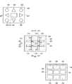
以下、本発明の実施の形態に係るタッチパネル入力装置について図面を参照しつつ説明する。図1は本発明の実施の形態に係るタッチパネル入力装置の概略的分解平面図、図2は同入力装置の概略的断面図、図3は同入力装置の設計変更例を示す概略的断面図、図4は同入力装置の別の設計変更例を示す概略的断面図である。 Hereinafter, a touch panel input device according to an embodiment of the present invention will be described with reference to the drawings. 1 is a schematic exploded plan view of a touch panel input device according to an embodiment of the present invention, FIG. 2 is a schematic cross-sectional view of the input device, FIG. 3 is a schematic cross-sectional view showing a design change example of the input device, FIG. 4 is a schematic cross-sectional view showing another design modification of the input device.
図1及び図2に示すタッチパネル入力装置は、基板100と、この基板100上にマトリックス状間隔を空けて配設されており且つ指の接近に応じて静電容量が各々変化する9個のセンサ電極200と、このセンサ電極200上にセットされる非電導性を有するスペーサ300と、このスペーサ300上にセットされる操作パネル400とを備えている。以下、各部を詳しく説明する。 The touch panel input device shown in FIGS. 1 and 2 includes a
基板100としてはリジット基板又はフレキシブル基板を用いる。 As the
スペーサ300は、ポリアミド(PA)樹脂、ポリカーボネート(PC)樹脂、ポリエチレンテレフタレート(PET)樹脂、ABS樹脂樹脂等で構成される板状の樹脂成形品である。この樹脂の比誘電率は3〜4である。 The
このスペーサ300は、9個のセンサ電極200の中央部に各々当接する部位である略矩形状の9つの第1のブロック310と、この第1のブロック310の間の部位である略矩形状の12つの第2のブロック320とを有する。 The
各第2のブロック320には、第1のブロック310の端部に沿って延びる長孔状のスリット321が設けられている。このスリット321により第1のブロック310の間にエアギャップが形成される。このエアギャップの空気の比誘電率は1である。 Each
操作パネル400は、ポリアミド(PA)樹脂、ポリカーボネート(PC)樹脂、ポリエチレンテレフタレート(PET)樹脂、ABS樹脂樹脂等で構成される板状の樹脂成形品である。この樹脂の比誘電率も3〜4である。 The
この操作パネル400の上面の中心部には、略長方形状の第1の操作突起410が設けられている。操作パネル400の第1の操作突起410の周囲には、略三角形状の4つの第2の操作突起420と、略円形状の4つの第3の操作突起430とが交互に設けられている。第1、第2、第3の操作突起410、420、430は、各センサ電極200の上方に位置するように配置されている。 A substantially rectangular
各センサ電極200は、基板100上に実装される銅箔あって、操作パネル400の第1の操作突起410、第2の操作突起420又は第3の操作突起430が指でタッチされる(即ち、指が接近する)と、前記指との間の静電容量が変化するようになっている。 Each
このセンサ電極200は、基板100上に設けられる図示しない信号処理回路に接続される。同回路により、指とセンサ電極200との間の静電容量の変化量を各々測定し、所定以上の静電容量の変化があった場合、操作パネル400の第1、第2、第3の操作突起410、420、430に指がタッチされたと検知するようになっている。 The
各センサ電極200の静電容量は次の数式から求められる。 The capacitance of each

例えば、図2に示すように、操作パネル400の第1の操作突起410が指でタッチされると、指と第1の操作突起410の下方に位置するセンサ電極200(即ち、図示中央のセンサ電極200)は、指と対向する面積(S)が大きく、指との距離(D)が近く且つ指との間の第1の操作突起410及びその下方の第1のブロック320の誘電率(ε)が3〜4であるため、指と中央のセンサ電極200との間の静電容量が大きく変化する。これに対し、前記センサ電極200の両隣のセンサ電極200(即ち、図示両端のセンサ電極200)は、指と対向する面積(S)が小さく、指との距離が遠く且つ指との間の前記エアギャップの誘電率(ε)が1であるため、指と両隣のセンサ電極200との間の静電容量の変化が小さくなる。 For example, as shown in FIG. 2, when the
この点、従来のタッチパネル入力装置による場合、複数のセンサ電極上に板状の操作パネルが存在していることから、前記操作パネルの指がタッチされた部位の下方に位置するセンサ電極と、その両隣のセンサ電極とは、指と対向する面積(S)及び指との距離(D)が異なるものの、指との間に存在する前記操作パネルの誘電率(ε)が同じになる。このため、センサ電極のピッチ間隔が狭くなると、前記センサ電極と指との間の静電容量の変化と同程度に、両隣のセンサ電極と指との間の静電容量が変化し、隣のセンサ電極の静電容量の変化に基づく誤入力の原因となっていた。 In this regard, in the case of the conventional touch panel input device, since a plate-like operation panel exists on the plurality of sensor electrodes, the sensor electrode positioned below the part touched by the finger of the operation panel, Although the adjacent sensor electrode has a different area (S) facing the finger and a distance (D) from the finger, the dielectric constant (ε) of the operation panel existing between the finger is the same. For this reason, when the pitch interval between the sensor electrodes is narrowed, the capacitance between the adjacent sensor electrode and the finger changes to the same extent as the change in capacitance between the sensor electrode and the finger. This was the cause of erroneous input based on the change in the capacitance of the sensor electrode.
これに対して、本タッチパネル入力装置による場合、センサ電極200のピッチ間隔が狭くなったとしても、操作パネル400の操作突起の下方のセンサ電極200の隣のセンサ電極200の静電容量の変化が、前記エアギャップにより、抑制される。このため、前記信号処理回路により、前記操作突起の下方のセンサ電極200の静電容量の大きな変化が測定され、センサ電極200上の操作突起がタッチされたと検知される一方、隣のセンサ電極200の静電容量の小さな変化が測定されても、隣のセンサ電極200上の操作突起がタッチされたと検知されない。このため、隣のセンサ電極200の静電容量の変化に基づく誤入力の発生を防止することができる。 On the other hand, in the case of this touch panel input device, even if the pitch interval of the
なお、上記実施例では、第2のブロック320にスリット321を設けてエアギャップを形成し、このエアギャップの空気の誘電体が第1のブロックの誘電率よりも低くなっているとしたが、これに限定されるものではない。即ち、第2のブロックは、第1のブロックの誘電率よりも低い素材で構成する限り任意に設計変更可能である。 In the above embodiment, the air gap is formed by providing the
また、第2のブロックを第1のブロックの誘電率よりも低い素材で構成するのに代えて、第2のブロックに導電部材(例えば、銅、鉄、ステンレス等の金属)を埋設(具体的には、インサート成型)し、当該金属をグランド接続するようにしても良い。この場合、指との間の静電容量の変化が隣のセンサ電極200に影響しないようにシールドすることができるため、前記エアギャップと同様の効果を得ることができる。 Also, instead of configuring the second block with a material having a lower dielectric constant than that of the first block, a conductive member (for example, a metal such as copper, iron, or stainless steel) is embedded in the second block (specifically, May be insert-molded) and the metal may be grounded. In this case, since it can shield so that the change of the electrostatic capacitance between fingers may not affect the
また、前記エアギャップは、第1のブロック310間の第2のブロック320にスリット321を設けることにより形成されるとしたが、これに限定されるものではない。例えば、図3に示すように、非電導部材である複数のスペーサ300’を複数のセンサ電極200の中央部上に各々セットし、当該スペーサ300’の間にエアギャップを形成するようにしても良い。The air gap is formed by providing the
上記実施例では、前記非電導部材はスペーサ300であるとして説明したが、これに限定されるものではない。例えば、図4に示すように、操作パネル400’の下面に第1、第2のブロックを設け、第2のブロックにスリットを形成するようにしても良い。また、操作パネルがタッチパネル入力装置の筐体と一体化されている場合、当該筐体に第1、第2のブロックを設け、第2のブロックにスリットを形成するようにしても良い。これらの場合であっても、スリットを設ける代わりに、前述のように、第2のブロックを誘電率が第1のブロックよりも低い素材で構成することができる。勿論、図3に示すスペーサ300’の代わりに前記操作パネル又は筐体を用いるようにしても良いが、センサ電極上にセットされる部分をテープ等で前記操作パネル本体又は筐体本体に取り付ける必要がある。なお、前記非電導部材として、操作パネルや筐体を用いる場合、スペーサ300は不要になる。In the said Example, although the saidnonelectroconductive member demonstrated as the
操作パネル400、400’については、第1、第2、第3の操作突起410、420、430が設けられているとしたが、これに限定されるものではない。例えば、前記操作パネルの操作面をフラット面とすることも可能である。操作パネルを筐体と一体化する場合も同様である。 The
第1のブロック310は、少なくともセンサ電極200の中央部に当接していれば良いが、センサ電極200の全面に当接するものを排除するものではない。なお、ここでいうセンサ電極200の中央部とは、センサ電極200の面上の周縁部を除く部分のことを言う。 The
スリット321は、スペーサ、操作パネル又は筐体の成型時にもうけるようにしても良いし、成型後にスリット加工するようにしても良い。この点は、前記スリットを操作パネル又は筐体に設ける場合も同様である。 The
また、センサ電極200については、指の接近に応じて静電容量が各々変化するものである限り任意に選択設定することが可能である。例えば、指の接近により、一対のセンサ電極の間の静電容量が変化するものであっても良い。この場合、前記非電導部材の第1のブロック又は前記非電導部材を一対のセンサ電極に各々当接させ、第2のブロック又は前記非電導部材の間のエアギャップを第1のブロックの間(即ち、一対の電極の周囲の上方又は下方位置)に配置するようにすれば良い。In addition, the
センサ電極200としては、上述した銅箔に限定されるものでない。例えば、操作パネルの面上に設けられる透明電極等とすることもできる。この場合も、前記透明電極に当接する部分を前記第1のブロックとし、第1のブロックの間の部分を前記第2のブロックとすれば良い。前記第2のブロックに前記スリットを設けるか、前記第2のブロックを第1のブロックより誘電率が低い素材とするかは任意に選択することが可能である。前述のように、操作パネルを透明電極に当接する複数のパーツに分割し、その間にエアギャップを形成する一方、前記パーツをテープ等で接続するようにしても構わない。なお、センサ電極として透明電極を設ける場合、基板100は不要になる。 The
センサ電極200の配列については、平面状に間隔を空けて並べられていれば良い。例えば、センサ電極200を一列に並べることも可能である。 As for the arrangement of the
なお、本発明に係るタッチパネル入力装置は、携帯通信端末のタッチパネル、カーナビゲーション用のタッチパネル、現金自動預け払い機用のタッチパネル、音楽携帯プレーヤ用のタッチパネル等に適応可能である。また、各部材の材質、個数、形状等については、上記実施例に限定されるものではない。 The touch panel input device according to the present invention can be applied to a touch panel of a mobile communication terminal, a touch panel for car navigation, a touch panel for an automatic teller machine, a touch panel for a portable music player, and the like. Further, the material, number, shape and the like of each member are not limited to the above embodiment.
100 基板
200 センサ電極
300 スペーサ(非電導部材)
310 第1のブロック
320 第2のブロック
321 スリット
400 操作パネル100
310
Claims (4)
Translated fromJapanese前記センサ電極上にセットされる非電導部材を備えており、
前記非電導部材は、少なくとも複数のセンサ電極の中央部に当接する部分である複数の第1のブロックと、
この第1のブロックの間の部分である複数の第2のブロックとを有しており、
前記第2のブロックにはスリットが設けられており、
このスリットに内在しており且つ前記非電導部材よりも比誘電率が低い空気により、前記第1のブロックの間にエアギャップが形成されている
ことを特徴とするタッチパネル入力装置。In a touch panel input device comprising a plurality of sensor electrodes whose capacitance changes eachbetween the finger in accordance with the proximity of and fingers arearranged at intervalson the substrate,
Comprising a non-conductive member set on the sensor electrode;
The non-conductive member includes a plurality of first blocks that are portions that contact at least central portions of the plurality of sensor electrodes;
A plurality of second blocks that are portions between the first blocks;
The second block is provided with a slit,
A touch panel input device, wherein an air gap is formed between the first blocks by air that is inherent in the slit and has a dielectric constant lower than that of the non-conductive member .
少なくとも複数のセンサ電極の中央部に各々当接する複数の非電導部材を備えており、
前記非電導部材の間に内在しており且つ該非電導部材よりも比誘電率が低い空気により、前記非電導部材の間にエアギャップが形成されている
ことを特徴とするタッチパネル入力装置。In a touch panel input device comprising a plurality of sensor electrodes whose capacitance changes eachbetween the finger in accordance with the proximity of and fingers arearranged at intervalson the substrate,
A plurality of non-conductive members eachabutting on the center of at least a plurality of sensor electrodes,
A touch panel input device, wherein an air gap is formed between the nonconductive members by air that is present between the nonconductive members and has a dielectric constant lower than that of the nonconductive members .
非電導部材は操作パネル又は筐体であることを特徴とするタッチパネル入力装置。The touch panel input device according to claim1 or 2 ,
The touch panel input device, wherein thenon-conductive member is an operation panel or a casing .
非電導部材上にセットされる操作パネル又は筐体を更に備えており、
非電導部材は操作パネル又は筐体と前記センサ電極との間に設けられるスペーサであることを特徴とするタッチパネル入力装置。The touch panel input device according to claim1 or 2 ,
It further includes an operation panel or a case set on the non-conductive member,
The touch panel input device, wherein the non-conductive member is a spacer provided between an operation panel or a casing and the sensor electrode .
Priority Applications (6)
| Application Number | Priority Date | Filing Date | Title |
|---|---|---|---|
| JP2007200344AJP4554651B2 (en) | 2007-08-01 | 2007-08-01 | Touch panel input device |
| TW097125732ATW200907773A (en) | 2007-08-01 | 2008-07-08 | Touch panel input device |
| US12/181,558US20090033636A1 (en) | 2007-08-01 | 2008-07-29 | Touch panel input device |
| KR1020080074896AKR20090013706A (en) | 2007-08-01 | 2008-07-31 | Touch Panel Input Device |
| EP08252606AEP2020631A3 (en) | 2007-08-01 | 2008-07-31 | Touch panel input device |
| CN2008101313012ACN101359907B (en) | 2007-08-01 | 2008-08-01 | Touch panel input device |
Applications Claiming Priority (1)
| Application Number | Priority Date | Filing Date | Title |
|---|---|---|---|
| JP2007200344AJP4554651B2 (en) | 2007-08-01 | 2007-08-01 | Touch panel input device |
Publications (2)
| Publication Number | Publication Date |
|---|---|
| JP2009037373A JP2009037373A (en) | 2009-02-19 |
| JP4554651B2true JP4554651B2 (en) | 2010-09-29 |
Family
ID=39926581
Family Applications (1)
| Application Number | Title | Priority Date | Filing Date |
|---|---|---|---|
| JP2007200344AExpired - Fee RelatedJP4554651B2 (en) | 2007-08-01 | 2007-08-01 | Touch panel input device |
Country Status (6)
| Country | Link |
|---|---|
| US (1) | US20090033636A1 (en) |
| EP (1) | EP2020631A3 (en) |
| JP (1) | JP4554651B2 (en) |
| KR (1) | KR20090013706A (en) |
| CN (1) | CN101359907B (en) |
| TW (1) | TW200907773A (en) |
Families Citing this family (32)
| Publication number | Priority date | Publication date | Assignee | Title |
|---|---|---|---|---|
| JP5098541B2 (en)* | 2007-09-28 | 2012-12-12 | カシオ計算機株式会社 | Capacitive touch panel |
| US20090278655A1 (en)* | 2008-05-06 | 2009-11-12 | The Abraham Joshua Heschel School | Method for inhibiting egress from a chamber containing contaminants |
| DE102008028313A1 (en)* | 2008-06-13 | 2009-12-17 | BSH Bosch und Siemens Hausgeräte GmbH | Capacitive touch switch for a household appliance |
| KR101583827B1 (en)* | 2009-03-10 | 2016-01-19 | 엘지이노텍 주식회사 | Input device |
| TWI392940B (en) | 2009-03-11 | 2013-04-11 | Au Optronics Corp | Pixel structure, touch display panel and liquid crystal display |
| FR2949007B1 (en)* | 2009-08-07 | 2012-06-08 | Nanotec Solution | DEVICE AND METHOD FOR CONTROL INTERFACE SENSITIVE TO A MOVEMENT OF A BODY OR OBJECT AND CONTROL EQUIPMENT INCORPORATING THIS DEVICE. |
| JP5466908B2 (en)* | 2009-09-21 | 2014-04-09 | 株式会社ワコム | Sensor substrate and position detection device |
| US8493349B2 (en)* | 2009-12-10 | 2013-07-23 | Lg Display Co., Ltd. | Touch screen panel |
| JP4918144B2 (en) | 2010-01-06 | 2012-04-18 | パナソニック株式会社 | Touch panel device and manufacturing method thereof |
| CN101840293B (en)* | 2010-01-21 | 2012-03-21 | 宸鸿科技(厦门)有限公司 | Scanning method for projected capacitive touch panels |
| JP5498811B2 (en)* | 2010-02-17 | 2014-05-21 | アルプス電気株式会社 | Capacitive input device |
| KR101148450B1 (en)* | 2010-03-02 | 2012-05-21 | 삼성전기주식회사 | Touch Screen for Vast Vision |
| JP5065431B2 (en) | 2010-03-31 | 2012-10-31 | キヤノン株式会社 | Image reading apparatus and operation panel |
| JP5038453B2 (en) | 2010-03-31 | 2012-10-03 | キヤノン株式会社 | Image reading apparatus and operation panel |
| JP5590974B2 (en) | 2010-06-08 | 2014-09-17 | キヤノン株式会社 | Operating device and image reading device |
| JP5595128B2 (en) | 2010-06-08 | 2014-09-24 | キヤノン株式会社 | Operating device and image reading device |
| WO2012012299A2 (en)* | 2010-07-21 | 2012-01-26 | Synaptics Incorporated | Producing capacitive images comprising non-connection values |
| US9041661B2 (en)* | 2010-08-13 | 2015-05-26 | Nokia Corporation | Cover for an electronic device |
| CN101976147B (en)* | 2010-09-30 | 2013-03-27 | 江苏惠通集团有限责任公司 | Touch recognition method, touch key structure and touch device |
| CN101963865B (en)* | 2010-09-30 | 2012-07-25 | 江苏惠通集团有限责任公司 | Touch identification method, touch key structure and touch device |
| JP5797025B2 (en)* | 2011-06-20 | 2015-10-21 | 日東電工株式会社 | Capacitive touch panel |
| CN102495681B (en)* | 2011-11-23 | 2014-07-09 | 江苏惠通集团有限责任公司 | Control equipment with touch buttons |
| JP5440618B2 (en)* | 2012-01-10 | 2014-03-12 | 株式会社デンソー | Input device |
| US8946985B2 (en) | 2012-05-07 | 2015-02-03 | Samsung Display Co., Ltd. | Flexible touch screen panel and flexible display device with the same |
| TW201415301A (en)* | 2012-10-03 | 2014-04-16 | Au Optronics Corp | Stylus, touch sensitive device and method for recognizing type of input element in contact with capacitive touch screen |
| CN105074863B (en) | 2013-04-01 | 2017-03-08 | 株式会社电装 | Capacitive switch |
| US9552090B2 (en) | 2014-02-05 | 2017-01-24 | Lg Innotek Co., Ltd. | Touch panel and display with the same |
| JP6384169B2 (en) | 2014-07-18 | 2018-09-05 | ブラザー工業株式会社 | Electronics |
| US10908742B2 (en)* | 2015-10-21 | 2021-02-02 | Microsoft Technology Licensing, Llc | Device with grooves in conductive casing |
| DE102016213868A1 (en)* | 2016-07-28 | 2018-02-01 | Bayerische Motoren Werke Aktiengesellschaft | Touch input device and electronic system for a motor vehicle and motor vehicle |
| KR102360850B1 (en)* | 2017-06-30 | 2022-02-10 | 삼성디스플레이 주식회사 | Touch sensor and display device including the touch sensor |
| KR20190012450A (en)* | 2017-07-27 | 2019-02-11 | 삼성전자주식회사 | Electronic device with fingerprint scan sensor |
Family Cites Families (16)
| Publication number | Priority date | Publication date | Assignee | Title |
|---|---|---|---|---|
| GB1443174A (en)* | 1973-04-06 | 1976-07-21 | Alphameric Keyboards Ltd | Keyboards for electronic circuits |
| US3965399A (en)* | 1974-03-22 | 1976-06-22 | Walker Jr Frank A | Pushbutton capacitive transducer |
| US4056699A (en)* | 1975-11-13 | 1977-11-01 | Essex International, Inc. | Touch plate assembly |
| JPS5682831U (en)* | 1979-11-30 | 1981-07-04 | ||
| US4439647A (en)* | 1982-07-14 | 1984-03-27 | Nick Calandrello | Touchpad keyboard |
| JPS6354619A (en)* | 1986-08-26 | 1988-03-09 | Daicel Chem Ind Ltd | Capacitance type coordinate detector |
| JP3651288B2 (en) | 1998-11-27 | 2005-05-25 | 松下電器産業株式会社 | INPUT DEVICE AND ELECTRONIC DEVICE USING THE SAME |
| KR100541009B1 (en)* | 2000-11-30 | 2006-01-10 | 니타 가부시키가이샤 | Capacitive sensor |
| WO2003088135A2 (en)* | 2002-04-15 | 2003-10-23 | Koninklijke Philips Electronics N.V. | Touch sensitive display device |
| US7154481B2 (en)* | 2002-06-25 | 2006-12-26 | 3M Innovative Properties Company | Touch sensor |
| WO2006068782A2 (en)* | 2004-12-22 | 2006-06-29 | 3M Innovative Properties Company | Touch sensors incorporating capacitively coupled electrodes |
| JP4456508B2 (en)* | 2005-03-22 | 2010-04-28 | アルプス電気株式会社 | Sensor |
| US7932898B2 (en)* | 2005-09-20 | 2011-04-26 | Atmel Corporation | Touch sensitive screen |
| JP2007122891A (en)* | 2005-10-25 | 2007-05-17 | Matsushita Electric Ind Co Ltd | Touch keys and electrical equipment using them |
| US20070229470A1 (en)* | 2006-03-31 | 2007-10-04 | Warren Snyder | Capacitive touch sense device having polygonal shaped sensor elements |
| US8599144B2 (en)* | 2006-07-31 | 2013-12-03 | Cypress Semiconductor Corporation | Grounded button for capacitive sensor |
- 2007
- 2007-08-01JPJP2007200344Apatent/JP4554651B2/ennot_activeExpired - Fee Related
- 2008
- 2008-07-08TWTW097125732Apatent/TW200907773A/enunknown
- 2008-07-29USUS12/181,558patent/US20090033636A1/ennot_activeAbandoned
- 2008-07-31EPEP08252606Apatent/EP2020631A3/ennot_activeWithdrawn
- 2008-07-31KRKR1020080074896Apatent/KR20090013706A/ennot_activeWithdrawn
- 2008-08-01CNCN2008101313012Apatent/CN101359907B/ennot_activeExpired - Fee Related
Also Published As
| Publication number | Publication date |
|---|---|
| US20090033636A1 (en) | 2009-02-05 |
| KR20090013706A (en) | 2009-02-05 |
| CN101359907B (en) | 2012-09-26 |
| CN101359907A (en) | 2009-02-04 |
| EP2020631A3 (en) | 2009-06-17 |
| EP2020631A2 (en) | 2009-02-04 |
| TW200907773A (en) | 2009-02-16 |
| JP2009037373A (en) | 2009-02-19 |
Similar Documents
| Publication | Publication Date | Title |
|---|---|---|
| JP4554651B2 (en) | Touch panel input device | |
| US9057653B2 (en) | Input device with force sensing | |
| US20110050631A1 (en) | Touch sensor | |
| US20140240616A1 (en) | Touch panel and manufacturing method thereof | |
| US20010055004A1 (en) | Flexible touchpad sensor grid for conforming to arcuate surfaces | |
| US20160054813A1 (en) | Low-profile capacitive pointing stick | |
| JP5482807B2 (en) | Capacitive touchpad with key switch | |
| US9910536B2 (en) | Touch sensor and touch panel device | |
| KR101905851B1 (en) | Capacitive switch | |
| US20170329434A1 (en) | Touch Panel | |
| CN107102764B (en) | Transcapacitive touch and force sensing in an input device | |
| JP2010086385A (en) | Capacitance sensor | |
| US9841859B2 (en) | Sensor structure and detection method | |
| JP5472858B2 (en) | Touch switch | |
| JP2016091803A (en) | Electrostatic capacity type input device | |
| KR20140110561A (en) | Wiring apparatus for touch screen panel | |
| JP2009026151A (en) | Input device and electronic appliance | |
| JP2018112854A (en) | Capacitance type sensor device | |
| US20160132180A1 (en) | Capacitive Touch Circuit and Touch Sensor and Capacitive Touch System Using The Same | |
| JP7026525B2 (en) | Sensor device | |
| CN106293136B (en) | Low-profile capacitive track point | |
| JP7344968B2 (en) | sensor device | |
| JP6392504B2 (en) | Control panel | |
| KR20110128533A (en) | Multi-layered Capacitive Input Device | |
| JP2014235927A (en) | Electrode for electrostatic touch switch device and electrostatic touch switch device |
Legal Events
| Date | Code | Title | Description |
|---|---|---|---|
| A621 | Written request for application examination | Free format text:JAPANESE INTERMEDIATE CODE: A621 Effective date:20090616 | |
| A977 | Report on retrieval | Free format text:JAPANESE INTERMEDIATE CODE: A971007 Effective date:20091209 | |
| A131 | Notification of reasons for refusal | Free format text:JAPANESE INTERMEDIATE CODE: A131 Effective date:20100105 | |
| A521 | Request for written amendment filed | Free format text:JAPANESE INTERMEDIATE CODE: A523 Effective date:20100302 | |
| TRDD | Decision of grant or rejection written | ||
| A01 | Written decision to grant a patent or to grant a registration (utility model) | Free format text:JAPANESE INTERMEDIATE CODE: A01 Effective date:20100713 | |
| A01 | Written decision to grant a patent or to grant a registration (utility model) | Free format text:JAPANESE INTERMEDIATE CODE: A01 | |
| A61 | First payment of annual fees (during grant procedure) | Free format text:JAPANESE INTERMEDIATE CODE: A61 Effective date:20100714 | |
| FPAY | Renewal fee payment (event date is renewal date of database) | Free format text:PAYMENT UNTIL: 20130723 Year of fee payment:3 | |
| R150 | Certificate of patent or registration of utility model | Free format text:JAPANESE INTERMEDIATE CODE: R150 | |
| LAPS | Cancellation because of no payment of annual fees |