JP4552810B2 - Semiconductor device - Google Patents
Semiconductor deviceDownload PDFInfo
- Publication number
- JP4552810B2 JP4552810B2JP2005257822AJP2005257822AJP4552810B2JP 4552810 B2JP4552810 B2JP 4552810B2JP 2005257822 AJP2005257822 AJP 2005257822AJP 2005257822 AJP2005257822 AJP 2005257822AJP 4552810 B2JP4552810 B2JP 4552810B2
- Authority
- JP
- Japan
- Prior art keywords
- leads
- plate
- semiconductor
- semiconductor elements
- lead
- Prior art date
- Legal status (The legal status is an assumption and is not a legal conclusion. Google has not performed a legal analysis and makes no representation as to the accuracy of the status listed.)
- Expired - Fee Related
Links
Images


Classifications
- H—ELECTRICITY
- H01—ELECTRIC ELEMENTS
- H01L—SEMICONDUCTOR DEVICES NOT COVERED BY CLASS H10
- H01L2224/00—Indexing scheme for arrangements for connecting or disconnecting semiconductor or solid-state bodies and methods related thereto as covered by H01L24/00
- H01L2224/01—Means for bonding being attached to, or being formed on, the surface to be connected, e.g. chip-to-package, die-attach, "first-level" interconnects; Manufacturing methods related thereto
- H01L2224/42—Wire connectors; Manufacturing methods related thereto
- H01L2224/44—Structure, shape, material or disposition of the wire connectors prior to the connecting process
- H01L2224/45—Structure, shape, material or disposition of the wire connectors prior to the connecting process of an individual wire connector
- H01L2224/45001—Core members of the connector
- H01L2224/45099—Material
- H01L2224/451—Material with a principal constituent of the material being a metal or a metalloid, e.g. boron (B), silicon (Si), germanium (Ge), arsenic (As), antimony (Sb), tellurium (Te) and polonium (Po), and alloys thereof
- H01L2224/45138—Material with a principal constituent of the material being a metal or a metalloid, e.g. boron (B), silicon (Si), germanium (Ge), arsenic (As), antimony (Sb), tellurium (Te) and polonium (Po), and alloys thereof the principal constituent melting at a temperature of greater than or equal to 950°C and less than 1550°C
- H01L2224/45144—Gold (Au) as principal constituent
- H—ELECTRICITY
- H01—ELECTRIC ELEMENTS
- H01L—SEMICONDUCTOR DEVICES NOT COVERED BY CLASS H10
- H01L2224/00—Indexing scheme for arrangements for connecting or disconnecting semiconductor or solid-state bodies and methods related thereto as covered by H01L24/00
- H01L2224/01—Means for bonding being attached to, or being formed on, the surface to be connected, e.g. chip-to-package, die-attach, "first-level" interconnects; Manufacturing methods related thereto
- H01L2224/42—Wire connectors; Manufacturing methods related thereto
- H01L2224/47—Structure, shape, material or disposition of the wire connectors after the connecting process
- H01L2224/48—Structure, shape, material or disposition of the wire connectors after the connecting process of an individual wire connector
- H01L2224/4805—Shape
- H01L2224/4809—Loop shape
- H01L2224/48091—Arched
- H—ELECTRICITY
- H01—ELECTRIC ELEMENTS
- H01L—SEMICONDUCTOR DEVICES NOT COVERED BY CLASS H10
- H01L2924/00—Indexing scheme for arrangements or methods for connecting or disconnecting semiconductor or solid-state bodies as covered by H01L24/00
- H01L2924/10—Details of semiconductor or other solid state devices to be connected
- H01L2924/11—Device type
- H01L2924/13—Discrete devices, e.g. 3 terminal devices
- H01L2924/1304—Transistor
- H01L2924/1305—Bipolar Junction Transistor [BJT]
- H01L2924/13055—Insulated gate bipolar transistor [IGBT]
- H—ELECTRICITY
- H01—ELECTRIC ELEMENTS
- H01L—SEMICONDUCTOR DEVICES NOT COVERED BY CLASS H10
- H01L2924/00—Indexing scheme for arrangements or methods for connecting or disconnecting semiconductor or solid-state bodies as covered by H01L24/00
- H01L2924/19—Details of hybrid assemblies other than the semiconductor or other solid state devices to be connected
- H01L2924/191—Disposition
- H01L2924/19101—Disposition of discrete passive components
- H01L2924/19107—Disposition of discrete passive components off-chip wires
Landscapes
- Lead Frames For Integrated Circuits (AREA)
Description
Translated fromJapanese本発明は、外部と電気的に接続するためのリードによって、Hブリッジ状に接続された複数の半導体素子の放熱を行うようにした半導体装置に関する。 The present invention relates to a semiconductor device in which a plurality of semiconductor elements connected in an H-bridge shape are radiated by leads for electrical connection to the outside.
本出願人は、先に出願した特願2004−291398号において、図10に示されるような半導体装置200を提案している。この半導体装置200は、パワーウィンドウの駆動モータを駆動するHIC(混成集積回路)に適用されるものである。 The present applicant has proposed a
図10(a)は半導体装置200の平面図、(b)は(a)のA−A断面図である。図10(a)に示されるように、先願の半導体装置200は、第1、第2電子素子210、220と、ヒートシンク230と、第1、第2配線基板240、250と、リード261、262と、を備えて構成されている。 10A is a plan view of the
第1電子素子210は、制御素子としてのマイコン211および制御IC212を備えている。また、第2電子素子220は、第1電子素子210よりも大きい電流が流れ、かつ、大きい発熱を行うものであり、例えばパワー素子としての4個のパワーMOS素子221〜224を備えている。このパワーMOS素子221〜224は、上記制御素子によって制御されるものであるとともに駆動モータを駆動する駆動素子として構成されている。 The first
この半導体装置200は、矩形板状のヒートシンク230を備えている。このヒートシンク230は、全体が鉄系金属で構成され、例えば純鉄(Fe)が用いられる。そして、ヒートシンク230の上面には、それぞれ分離された第1配線基板240、第2配線基板250が搭載されている。これら第1、第2配線基板240、250として、例えば積層構造のセラミック基板が用いられ、例えば、電気絶縁性を有しかつ熱伝導性に優れた樹脂などからなる接着剤によってヒートシンク230の上面に固定されている。これら第1、第2配線基板240、250は、それぞれ熱的にも分離されている。 The
そして、第1電子素子210としての制御素子は、第1配線基板240の上に実装され、第2電子素子220としてのパワーMOS素子221〜224は、第1配線基板240とは分離された第2配線基板250の上に実装されている。これら第1、第2電子素子210、220は、例えばはんだを介して第1、第2配線基板240、250にそれぞれ固定されている。 The control element as the first
また、図10(a)に示されるように、ヒートシンク230の外周において制御素子の周囲には、複数本の信号端子としてのリード261が設けられており、パワーMOS素子221〜224の周囲には、複数本の電流端子としてのリード262が設けられている。リード261は、制御端子であるマイコン211や制御IC212と電気的に接続されるものであり、リード262は、パワー素子である各パワーMOS素子221〜224と電気的に接続されるものである。 Also, as shown in FIG. 10A, a plurality of
これらリード261、262と第1、第2電子素子210、220とは、図10(b)に示されるように、ボンディングワイヤ270により結線され、電気的に接続されている。なお、図10(a)では、このボンディングワイヤ270を省略してある。 These leads 261 and 262 and the first and second
そして、第1、第2電子素子210、220、第1、第2配線基板240、250、ボンディングワイヤ270、リード261、262におけるボンディングワイヤ270との接続部、および、ヒートシンク230は、樹脂280によってモールドされている。 The first and second
このような構成を有する半導体装置200において、第1電子素子210よりも大きな熱を放出する第2電子素子220の熱は、セラミック基板である第1、第2配線基板240、250およびヒートシンク230を介して例えばモータの筐体に放熱されるようになっている。 In the
しかしながら、上記のように第1、第2配線基板240、250およびヒートシンク230を介して放熱する場合、以下のような問題が生じることが本発明者らの検討により明らかとなった。 However, when the heat is radiated through the first and
すなわち、上述のように、第2配線基板250はセラミック材料で形成されたセラミック基板で構成され、ヒートシンク230は金属で構成されている。このため、セラミック基板としての第2配線基板250の熱伝導が金属(Fe)で構成されるヒートシンク230より劣ってしまい、第2電子素子220で発生した熱の熱エネルギーは第2配線基板250からヒートシンク230にスムーズに移動しなくなっている。 That is, as described above, the
また、ヒートシンク230と第2配線基板250とは材質が異なるものであるため、接着剤を用いて第2配線基板250をヒートシンク230に固定している。このため、この接着剤による接合部分の熱抵抗が上昇してしまい、第2配線基板250からヒートシンク230に熱が効率的に伝わらず、放熱性が低下してしまっている。 Further, since the
さらに、放熱のためにヒートシンク230を用いているため、半導体装置200のサイズが大きくなってしまっている。 Furthermore, since the
本発明は、上記点に鑑み、パワー素子を備えた半導体装置において、パワー素子の放熱性を向上させることを第1の目的とし、半導体装置のサイズを小型化することを第2の目的とする。 In view of the above points, the present invention has a first object to improve heat dissipation of a power element in a semiconductor device including a power element, and a second object to reduce the size of the semiconductor device. .
上記目的を達成するため、本発明では、各半導体素子(11〜14)の各第1、第2電極それぞれに金属リード(21〜24、31〜34、41〜44、101〜105、111、112、121〜123、131〜134)がそれぞれ直接接合されていることを特徴とする。 In order to achieve the above object, in the present invention, metal leads (21-24, 31-34, 41-44, 101-105, 111, 111) are provided on the first and second electrodes of the semiconductor elements (11-14), respectively. 112, 121-123, 131-134) are directly joined to each other.
このように、各半導体素子の上下の面に設けられた各第1、第2電極に、ヒートシンクとしての役割を果たす金属リードを直接接合する。これにより、半導体素子と金属リードとの接合部分の熱抵抗を低減でき、半導体素子と金属リードとの間で熱エネルギーをスムーズに移動させることができる。したがって、半導体素子の上下の各面から金属リードを介して半導体素子で発生した熱を樹脂外部に導くことができ、半導体素子の放熱性を向上させることができる。 In this way, metal leads that serve as heat sinks are directly joined to the first and second electrodes provided on the upper and lower surfaces of each semiconductor element. Thereby, the thermal resistance of the junction part of a semiconductor element and a metal lead can be reduced, and a thermal energy can be moved smoothly between a semiconductor element and a metal lead. Therefore, the heat generated in the semiconductor element can be guided to the outside of the resin from the upper and lower surfaces of the semiconductor element via the metal leads, and the heat dissipation of the semiconductor element can be improved.
また、半導体装置においてヒートシンクを用いずに半導体素子で発生する熱を外部に放出することができ、かつ、各半導体素子を積層状に配置させているので、半導体装置のサイズを小型化することができる。 In addition, the heat generated in the semiconductor element can be released to the outside without using a heat sink in the semiconductor device, and each semiconductor element is arranged in a stacked manner, so that the size of the semiconductor device can be reduced. it can.
本発明では、各半導体素子(11〜14)と基板(81)に設けられた電気回路とはワイヤ(51〜54、71〜74)および中継リード(61〜64)を介して電気的に接続されていることを特徴とする。 In the present invention, each semiconductor element (11-14) and the electric circuit provided on the substrate (81) are electrically connected via wires (51-54, 71-74) and relay leads (61-64). It is characterized by being.
このように、各半導体素子と電気回路とをワイヤおよび中継リードを介して電気的に接続する形態とする。これにより、電子素子にて各半導体素子を駆動制御することができる。 Thus, each semiconductor element and the electric circuit are electrically connected via the wire and the relay lead. Thereby, each semiconductor element can be driven and controlled by the electronic element.
本発明では、各半導体素子は、MOS構造のパワー素子として形成されたものであることを特徴とする。 In the present invention, each semiconductor element is formed as a power element having a MOS structure.
このように、半導体素子としてMOS構造のパワー素子を採用する。このような発熱量の大きい素子を半導体装置に採用したとしても、上記のように、各金属リードによって各半導体素子で発生する熱を放熱することができる。 In this way, a MOS power element is employed as the semiconductor element. Even if such an element with a large calorific value is employed in a semiconductor device, the heat generated in each semiconductor element can be dissipated by each metal lead as described above.
本発明では、各半導体素子の各第1電極にリボンリード(21〜24)のうちの一部がそれぞれ直接接合され、リボンリードのうち各半導体素子の各第1電極に接合されていない部分の一部が板状リード(31〜34、111、112、123)に接合されている。また、リボンリードが接合された板状リードとは別の板状リード(41〜44、121、122)が各半導体素子の各第2電極にそれぞれ直接接合されていることを特徴とする。 In the present invention, a part of the ribbon leads (21 to 24) is directly joined to each first electrode of each semiconductor element, and a portion of the ribbon lead that is not joined to each first electrode of each semiconductor element. A part is joined to the plate-like leads (31 to 34, 111, 112, 123). Further, a plate-like lead (41 to 44, 121, 122) different from the plate-like lead to which the ribbon lead is joined is directly joined to each second electrode of each semiconductor element.
このように、金属リードを板状リード、リボンリードとして用意し、半導体素子の第1、第2電極にそれぞれ接合する。これにより、半導体素子で発生した熱を、半導体素子にそれぞれ直接接合された板状リードおよびリボンリードを介して放熱することができる。 Thus, the metal leads are prepared as plate-like leads and ribbon leads, and are joined to the first and second electrodes of the semiconductor element, respectively. Thereby, the heat generated in the semiconductor element can be dissipated through the plate-like lead and the ribbon lead directly bonded to the semiconductor element.
本発明では、リボンリード(21、23)を介して第1および第3半導体素子(11、13)の各第1電極にそれぞれ各板状リード(31、33)が接続され、これら板状リードが互いに張り合わされる。また、第1〜第4半導体素子の各第2電極にそれぞれ接合された各板状リード(41〜44)のうち、第1および第2半導体素子(11、12)が接合された板状リード(41、42)が互いに張り合わされ、第3および第4半導体素子(13、14)が接合された板状リード(43、44)が互いに張り合わされる。そして、リボンリード(22、24)を介して第2および第4半導体素子(12、14)の各第1電極に各板状リード(32、34)がそれぞれ接続されていることを特徴とする。 In the present invention, the plate-like leads (31, 33) are connected to the first electrodes of the first and third semiconductor elements (11, 13) via the ribbon leads (21, 23), respectively. Are stuck together. Of the plate-like leads (41 to 44) joined to the second electrodes of the first to fourth semiconductor elements, the plate-like leads to which the first and second semiconductor elements (11, 12) are joined. (41, 42) are stuck together, and the plate-like leads (43, 44) to which the third and fourth semiconductor elements (13, 14) are joined are stuck together. The plate-like leads (32, 34) are connected to the first electrodes of the second and fourth semiconductor elements (12, 14) via the ribbon leads (22, 24), respectively. .
このようにして、各半導体素子それぞれにリボンリードや板状リードを接合する。これにより、各半導体素子で発生する熱をリボンリードおよび板状リードを介して放熱することができる。 Thus, a ribbon lead or a plate-like lead is bonded to each semiconductor element. Thereby, the heat generated in each semiconductor element can be dissipated through the ribbon lead and the plate-like lead.
本発明では、第1および第2半導体素子(11、12)の組と、前記第3および第4半導体素子(13、14)の組と、が横並びで配置された状態で、リボンリード(21、23)を介して第1および第3半導体素子(11、13)の各第1電極にそれぞれ共通の板状リード(112)が接続されていると共に、リボンリード(22、24)を介して第2および第4半導体素子(12、14)の各第1電極にそれぞれ共通の板状リード(111)が接続されていることを特徴とする。 In the present invention, the ribbon lead (21) in a state where the set of the first and second semiconductor elements (11, 12) and the set of the third and fourth semiconductor elements (13, 14) are arranged side by side. 23), a common plate-like lead (112) is connected to the first electrodes of the first and third semiconductor elements (11, 13) via the ribbon leads (22, 24). A common plate-like lead (111) is connected to each first electrode of the second and fourth semiconductor elements (12, 14).
このように、各半導体素子に接続する板状リードの共通化を図る。これにより、使用する板状リードの数を削減することができ、各半導体素子に対する板状リードの組み付けを容易に行うことができる。 In this way, the plate-like lead connected to each semiconductor element is made common. Thereby, the number of the plate-like leads to be used can be reduced, and the plate-like leads can be easily assembled to the respective semiconductor elements.
本発明では、第1および第3半導体素子に接続される板状リード(112)と、第2および第4半導体素子に接続される板状リード(111)とは、それぞれT字形状になっていることを特徴とする。 In the present invention, the plate-like lead (112) connected to the first and third semiconductor elements and the plate-like lead (111) connected to the second and fourth semiconductor elements are each T-shaped. It is characterized by being.
このように、各板状リード(111、112)がそれぞれT字形状になっている。これにより、横並びにされた各半導体素子(例えば第1半導体素子(11)と第3半導体素子(13))にT字形状の板状リードを容易に接続でき、各半導体素子に共通の端子として用いることができる。 Thus, each plate-like lead (111, 112) has a T-shape. Thereby, a T-shaped plate-like lead can be easily connected to each of the semiconductor elements arranged side by side (for example, the first semiconductor element (11) and the third semiconductor element (13)), and as a common terminal for each semiconductor element. Can be used.
本発明では、リボンリード(22)を介して第2半導体素子(12)の第1電極に板状リード(32、103)が接続され、第2半導体素子の第2電極に板状リード(102、121)が直接接合され、この板状リードの裏面に第1半導体素子(11)の第2電極が直接接合されている。また、第1半導体素子の第1電極にリボンリード(21)を介して板状リード(101、123)が接続され、この板状リードの裏面にリボンリード(23)を介して第3半導体素子(13)の第1電極が接続されている。さらに、第3半導体素子の第2電極に板状リード(104、122)が直接接合され、この板状リードの裏面に第4半導体素子(14)の第2電極が直接接合される。そして、第4半導体素子の第1電極にリボンリード(24)を介して板状リード(34、105)が接続されていることを特徴とする。 In the present invention, the plate-like lead (32, 103) is connected to the first electrode of the second semiconductor element (12) via the ribbon lead (22), and the plate-like lead (102) is connected to the second electrode of the second semiconductor element. 121) are directly joined, and the second electrode of the first semiconductor element (11) is joined directly to the back surface of the plate-like lead. Further, plate-like leads (101, 123) are connected to the first electrode of the first semiconductor element via a ribbon lead (21), and the third semiconductor element is connected to the back surface of the plate-like lead via a ribbon lead (23). The first electrode of (13) is connected. Furthermore, the plate-like lead (104, 122) is directly joined to the second electrode of the third semiconductor element, and the second electrode of the fourth semiconductor element (14) is directly joined to the back surface of the plate-like lead. A plate-like lead (34, 105) is connected to the first electrode of the fourth semiconductor element via a ribbon lead (24).
このように、半導体装置を構成する。これにより、第1、第2負荷接続用端子としての板状リード(102、104、121、122)および電源端子としての板状リード(101、123)を共通化することができ、半導体装置の構成を簡略化することができる。 Thus, the semiconductor device is configured. Thereby, the plate-like leads (102, 104, 121, 122) as the first and second load connection terminals and the plate-like leads (101, 123) as the power supply terminals can be shared, and the semiconductor device The configuration can be simplified.
本発明では、金属リードは、金属板の一端側が薄肉化されたリボンリード部(131a〜134a)が半導体素子の第1電極に直接接合されると共に、板状リード(41〜44)の一端側が第2電極に直接接合されていることを特徴とする。 In the present invention, in the metal lead, the ribbon lead portion (131a to 134a) whose one end side of the metal plate is thinned is directly joined to the first electrode of the semiconductor element, and the one end side of the plate-like lead (41 to 44) is It is characterized by being directly joined to the second electrode.
このように、金属リードを板状リード、加工リードとして用意し、半導体素子の第1、第2電極にそれぞれ接合する。これにより、半導体素子で発生した熱を、半導体素子にそれぞれ直接接合された板状リードおよび加工リードを介して放熱することができる。 In this way, the metal leads are prepared as plate-like leads and processed leads, and are joined to the first and second electrodes of the semiconductor element, respectively. Thereby, the heat generated in the semiconductor element can be dissipated through the plate-like lead and the processing lead directly joined to the semiconductor element.
本発明では、第1および第3半導体素子(11、13)の各第1電極にリボンリード部(133a、134a)がそれぞれ直接接合された各加工リード(133、134)が互いに張り合わされると共に、第1、第2半導体素子(11、12)の各第2電極にそれぞれ直接接合された各板状リード(41、42)、および第3、第4半導体素子(13、14)の各第2電極にそれぞれ直接接合された各板状リード(43、44)が互いに張り合わされる。また、第2および第4半導体素子(12、14)の各第1電極に各加工リード(131、132)のリボンリード部(131a、132a)がそれぞれ直接接合されていることを特徴とする。 In the present invention, the processing leads (133, 134) in which the ribbon lead portions (133a, 134a) are directly bonded to the first electrodes of the first and third semiconductor elements (11, 13) are bonded to each other. The plate-like leads (41, 42) directly joined to the second electrodes of the first and second semiconductor elements (11, 12), and the third leads of the third and fourth semiconductor elements (13, 14), respectively. The plate-like leads (43, 44) directly joined to the two electrodes are attached to each other. Further, the ribbon lead portions (131a, 132a) of the processing leads (131, 132) are directly joined to the first electrodes of the second and fourth semiconductor elements (12, 14), respectively.
このように、各半導体素子それぞれに各加工リードのリボンリード部や板状リードを直接接合する。これにより、各半導体素子で発生する熱をリボンリード部および板状リードを介して放熱することができる。 In this way, the ribbon lead portion and plate-like lead of each processing lead are directly joined to each semiconductor element. Thereby, the heat generated in each semiconductor element can be dissipated through the ribbon lead portion and the plate-like lead.
本発明では、互いに張り合わされる板状リード(31、33、41〜44)もしくは加工リード(133、134)において、互いに張り合わされる面のうち一方に凹部が設けられ、他方に前記凹部と対応する凸部が設けられている。そして、板状リードもしくは加工リードが張り合わされたとき、一方の板状リードもしくは加工リードに設けられた凹部に他方の板状リードもしくは加工リードに設けられた凸部が嵌合することを特徴とする。 In the present invention, in the plate-like leads (31, 33, 41 to 44) or the processed leads (133, 134) that are attached to each other, a recess is provided on one of the surfaces that are attached to each other, and the other corresponds to the recess. Protruding parts are provided. And, when the plate-like lead or the processed lead is pasted together, the convex portion provided on the other plate-shaped lead or the processed lead is fitted into the concave portion provided on the one plate-shaped lead or the processed lead. To do.
このように、互いに張り合わされる板状リードもしくは加工リードの表面に凹凸形状を設けて嵌合する。これにより、各板状リードもしくは加工リードを張り合わせたときに互いの板状リードもしくは加工リードを密着させやすくすることができる。 In this manner, the surface of the plate-like lead or the processed lead that is bonded to each other is provided with an uneven shape and fitted. Thereby, when each plate-like lead or processing lead is bonded, it is possible to make the plate-like leads or processing leads close to each other.
本発明では、板状リード(31〜34、41〜44、101〜105、111、112、121〜123)もしくは加工リード(131〜134)は、樹脂から露出した部分が同一平面上にそれぞれ配置されるように、樹脂内で曲げ加工が施されていることを特徴とする。 In the present invention, the plate-like leads (31 to 34, 41 to 44, 101 to 105, 111, 112, 121 to 123) or the processed leads (131 to 134) are arranged on the same plane with portions exposed from the resin, respectively. As described above, bending is performed in the resin.
このように、樹脂から露出する部分が同一平面上に配置されるように板状リードもしくは加工リードにそれぞれ曲げ加工を施す。これにより、半導体装置を外部回路に接続しやすい形態とすることができる。 In this manner, the plate-like lead or the processed lead is bent so that the portions exposed from the resin are arranged on the same plane. Thus, the semiconductor device can be easily connected to an external circuit.
なお、上記各手段の括弧内の符号は、後述する実施形態に記載の具体的手段との対応関係を示すものである。 In addition, the code | symbol in the bracket | parenthesis of each said means shows the correspondence with the specific means as described in embodiment mentioned later.
以下、本発明の実施形態について図に基づいて説明する。なお、以下の各図相互において、互いに同一もしくは均等である部分には、説明の簡略化を図るべく、図中、同一符号を付してある。 Hereinafter, embodiments of the present invention will be described with reference to the drawings. In the following drawings, parts that are the same or equivalent to each other are given the same reference numerals in the drawings for the sake of simplicity.
(第1実施形態)
以下、本発明の第1実施形態について図を参照して説明する。本実施形態で示される半導体装置は、パワーウィンドウの駆動モータを駆動するHICに適用される。(First embodiment)
Hereinafter, a first embodiment of the present invention will be described with reference to the drawings. The semiconductor device shown in this embodiment is applied to an HIC that drives a drive motor for a power window.
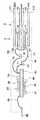
図1は、本発明の第1実施形態に係る半導体装置の概略断面図である。この図に示されるように、半導体装置1は、第1〜第4半導体素子11〜14を備えている。これら各半導体素子11〜14は、矩形板状をなすものであり、例えばシリコン半導体などの半導体基板に発熱量が大きいMOS構造を有するパワー素子が形成されている。 FIG. 1 is a schematic cross-sectional view of a semiconductor device according to the first embodiment of the present invention. As shown in this figure, the
具体的に、各半導体素子11〜14のうち第1、第3半導体素子11、13にはPch(Pチャンネル)型DMOS素子が形成され、第2、第4半導体素子12、14にはNch(Nチャンネル)型DMOS素子が形成されている。これら各半導体素子11〜14は、Hブリッジ回路を構成するように電気的接続がなされている。 Specifically, among the
なお、Pch型DMOS素子はゲート電圧がソース電圧よりも低いときに電流が流れるタイプのものであり、Nch型DMOS素子はゲート電圧がソース電圧よりも高いときに電流が流れるタイプのものである。 The Pch type DMOS element is of a type in which current flows when the gate voltage is lower than the source voltage, and the Nch type DMOS element is of a type in which current flows when the gate voltage is higher than the source voltage.
これら各半導体素子11〜14に設けられた図示しないソースパッド(本発明の第1電極)には、例えばはんだ付けによってそれぞれリボンリード21〜24が接合されている。このリボンリード21〜24は例えばAl(アルミニウム)などの熱伝導性の良い金属板で構成されており、例えば厚さが0.1mm程度もしくはそれ以下のものが用いられる。 Ribbon leads 21 to 24 are joined to source pads (first electrodes of the present invention) provided in the
そして、各リボンリード21〜24のうちの一部が各半導体素子11〜14の各ソースパッドにはんだ付けによって接合され、リボンリード21〜24のうち各ソースパッドに接合されていない部分の一部がそれぞれリード31〜34に接合されている。これらリード31〜34は、例えばCu(銅)などの熱伝導性の良い金属板で構成されており、例えば厚さが0.3〜1.0mmのものが用いられる。 A part of each of the ribbon leads 21 to 24 is joined to each source pad of each of the
また、各半導体素子11〜14のうちソースパッドが設けられた面とは反対側の面に図示しないドレインパッド(本発明の第2電極)がそれぞれ設けられており、これらドレインパッドにそれぞれリード41〜44が接合されている。 Also, a drain pad (second electrode of the present invention) (not shown) is provided on the surface of each of the
上記第1、第2半導体素子11、12の各ドレインパッドにそれぞれ接続されたリード41、42のうち各半導体素子11、12が接合された面とは反対側の面がそれぞれ張り合わされて密着した状態になっている。具体的には、各リード41、42において互いに張り合わされる面のうち一方に凹部が設けられ、他方に前記凹部と対応する凸部が設けられており、これらリード41、42が張り合わされたとき、一方に設けられた凹部に他方に設けられた凸部が嵌合するようになっている。このように、互いに張り合わせるリード41、42の表面それぞれに凹凸形状を設けることで、各リード41、42を張り合わせたときに互いのリード41、42を密着させやすくすることができる。 Of the
同様に、リボンリード21、23を介して第1、第3半導体素子11、13のソースパッドにそれぞれ電気的に接続されたリード31、33のうち、リボンリード21、23が接合された面とは反対側の面がそれぞれ張り合わされた状態になっている。さらに、第3、第4半導体素子13、14の各ドレインパッドにそれぞれ接続されたリード43、44のうち各半導体素子13、14が接合された面とは反対側の面がそれぞれ張り合わされて密着した状態になっている。このようにして張り合わされた各リード31、3343、44には、上述のように凹凸が設けられ、張り合わされた各リード31、33、43、44同士がそれぞれ密着しやすくなっている。 Similarly, of the
本実施形態では、リボンリード22、24を介して第2、第4半導体素子12、14のソースパッドにそれぞれ電気的に接続されたリード32、34をそれぞれGND(グランド)端子とする。また、第1、第2半導体素子11、12の各ドレインパッドにそれぞれ接合された各リード41、42をM1端子とし、第3、第4半導体素子13、14の各ドレインパッドにそれぞれ接合された各リード43、44をM2端子とする。そして、リボンリード21、23を介して第1、第3半導体素子11、13の各ドレインパッドにそれぞれ電気的に接続された各リード31、33をVdd端子とする。 In the present embodiment, the
上記のようにして各半導体素子11〜14に電気的に接続されたリボンリード21〜24およびリード31〜34、41〜44は、上述のように熱伝導性の良い、すなわち放熱性が高い金属板で構成されているため、各半導体素子11〜14で発生した熱を外部に放出するためのヒートシンクとしての役割も果たすようになっている。 The ribbon leads 21 to 24 and the
したがって、各半導体素子11〜14の各ソースパッドに各リボンリード21〜24が接合されていると共に、各リボンリード21〜24が各リード31〜34に接合され、かつ、各半導体素子11〜14の各ドレインパッドに各リード41〜44が接合されていることで、各半導体素子11〜14で発生した熱を各ソースパッド面および各ドレインパッド面の両面から直接リボンリード21〜24およびリード31〜34、41〜44を介して外部に放熱できるようになっている。 Therefore, the ribbon leads 21 to 24 are bonded to the source pads of the
また、各半導体素子11〜14において、それぞれソースパッドが設けられた面と同じ面に図示しないゲートパッドがそれぞれ設けられている。これら各半導体素子11〜14の各ゲートパッドにはそれぞれワイヤ51〜54が接合されており、これらワイヤ51〜54はそれぞれ中継リード61〜64に接続されている。さらに、各中継リード61〜64にはそれぞれワイヤ71〜74が接続され、各ワイヤ71〜74はそれぞれ積層基板81に電気的に接続されている。 Each of the
上記積層基板81は、積層構造をなしており、その内部に電気回路を備えたものとして構成されているものである。この積層基板81には、上記各半導体素子11〜14を駆動するための駆動用チップ82が設置されている。この駆動用チップ82は、ワイヤ83、84を介して積層基板81内の電気回路に接続されている。なお、積層基板81は図示しないフレームに搭載された状態になっている。 The
また、積層基板81において、駆動用チップ82が設置された面とは反対側の面に駆動用チップ82を制御駆動するためのマイクロコンピュータチップ(以下、マイコンチップという)85が設置されている。このマイコンチップ85は、ワイヤ86、87を介して積層基板81内の電気回路に接続されている。上記駆動用チップ82およびマイコンチップ85は例えばAgペーストにより積層基板81に搭載されている。 In the
さらに、積層基板81内の電気回路は、ワイヤ88を介してリード89に電気的に接続されている。これにより、外部からの信号が、積層基板81内の電気回路を介してマイコンチップ85および駆動用チップ82に入力されるようになっている。なお、リード89は、紙面垂直方向に複数配置されている。 Further, the electric circuit in the
本実施形態では、ワイヤ51〜54、71〜74、83、84、86〜88として例えばAuワイヤが採用される。 In this embodiment, Au wires are employed as the
そして、各リード31〜34、41〜44、89の端部が露出するように積層基板81や中継リード61〜64、そして各半導体素子11〜14が樹脂90にてモールドされている。なお、図1において、樹脂90の外壁部分は破線で示されており、この破線の内部に樹脂90が充填されている。以上が、本実施形態に係る半導体装置1の構成である。 The
なお、本実施形態のリード31〜34、41〜44およびリボンリード21〜24は本発明の金属リードに相当し、さらにリード31〜34、41〜44は本発明の板状リードに相当する。また、駆動用チップ82およびマイコンチップ85は本発明の電子素子に相当する。さらに、M1、M2端子は本発明の第1、第2負荷接続用端子に相当し、Vdd端子は本発明の電源端子、GND端子は本発明の接地用端子に相当する。 The leads 31 to 34 and 41 to 44 and the ribbon leads 21 to 24 of the present embodiment correspond to the metal leads of the present invention, and the
続いて、上記半導体装置1の製造方法について図を参照して説明する。図2は、図1に示される半導体装置1の製造工程を示した図である。 Next, a method for manufacturing the
まず、中継リード62とリード42が外部ダイバーで繋がっている図示しないフレームを用意する。そして、図2(a)に示す工程では、リード42に第2半導体素子12をはんだ付けによって接合する。具体的には、リード42の所定箇所にあらかじめくぼみを設け、このくぼみに第2半導体素子12のドレインパッドをはんだ付けする。 First, a frame (not shown) in which the
なお、リード42の表面にNiメッキ等を施しておくことで、第2半導体素子12をリード42にはんだ付けしやすくすることができる。また、リード42として例えば厚さ0.3〜1.0mmのCuの金属板を用いる。 In addition, it is possible to easily solder the
この後、ボンディング装置で、第2半導体素子12のゲートパッドと中継リード62との間をワイヤ52でワイヤボンドすると共に、第2半導体素子12のソースパッド上にリボンリード22をはんだ付けする。上述のように、リボンリード22として例えば厚さが0.1mm以下のAlの金属板を用いる。 Thereafter, the bonding pad is used to wire bond between the gate pad of the
そして、図2(a)に示されるものを、第1〜第4半導体素子11〜14それぞれについて用意する。 And what is shown by Fig.2 (a) is prepared about each of the 1st-4th semiconductor elements 11-14.
図2(b)に示す工程では、M1端子を構成する。すなわち、第1、第2半導体素子11、12にそれぞれ接合されたリード41、42を張り合わせる。具体的には、各リード41、42のうち第1、第2半導体素子11、12が接合された面とは反対側の面をそれぞれ張り合わせる。 In the step shown in FIG. 2B, the M1 terminal is configured. That is, the
この際、各リード41、42のうち第1、第2半導体素子11、12が接合された面とは反対側の面にあらかじめ凹凸を設けておくことで各リード41、42を密着させやすくすることができる。このようにして、M1端子を構成する。同様に、第3、第4半導体素子13、14においても各リード43、44をそれぞれ張り合わせてM2端子を構成する。 At this time, it is easy to make the
図2(c)に示す工程では、GND端子およびVdd端子を構成する。具体的には、第1、第2半導体素子11、12が用いられて形成された図2(b)に示されるものをスペーサ治具で固定し、例えば各リード41、42と各リード31、32との位置関係を決め、各リボンリード21、22にリード31、32をそれぞれはんだ付けまたは溶接で接合する。これにより、GND端子およびVdd端子を形成できる。 In the step shown in FIG. 2C, a GND terminal and a Vdd terminal are formed. Specifically, the one shown in FIG. 2B formed by using the first and
同様に、第3、第4半導体素子13、14が用いられて形成された図2(b)に示されるものを用意し、各リボンリード23、24に各リード33、34を接合して図2(c)に示されるものを形成する。 Similarly, the one shown in FIG. 2B formed using the third and
この後、図示しないが、リボンリード21を介して第1半導体素子11に電気的に接続されたVdd端子としてのリード31と、リボンリード23を介して第3半導体素子13に電気的に接続されたVdd端子としてのリード33と、をリボンリード21、23が接合された面とは反対側の面をそれぞれ張り合わせることにより、1つのVdd端子を構成する。以上のようにして、図1に示されるHブリッジ回路部分が完成する。 Thereafter, although not shown, the
そして、積層基板81に駆動用チップ82およびマイコンチップ85を搭載してワイヤボンドしたものを用意し、Hブリッジ回路部分と積層基板81との位置関係をボンディング装置の冶具で固定して決定する。この後、ボンディング装置で、各中継リード61〜64と積層基板81内の電気回路との間を各ワイヤ71〜74でワイヤボンドする。こうして、Hブリッジ回路部分と積層基板81とを中継リード61〜64およびワイヤ51〜54、71〜74を介して電気的に接続することができる。 Then, a device in which the
次に、外部から信号を入力するためのリード89と積層基板81内の電気回路とをワイヤ88でワイヤボンドし、リード31〜34、41〜44、89の端部が露出するように積層基板81、中継リード61〜64、そしてHブリッジ回路部分を樹脂90にてモールドする。こうして、図1に示される半導体装置1が完成する。 Next, the
上記半導体装置1の構成において、第1〜第4半導体素子11〜14によって構成される回路について説明する。図3は、第1〜第4半導体素子11〜14にて構成されるHブリッジ回路部分の回路図を示したものである。 In the configuration of the
図3に示されるように、各半導体素子11〜14は、Hブリッジ回路を構成している。また、本半導体装置1には、車の窓ガラスを駆動させるための上記モータMOや図示しない装置の電源が設けられている。 As shown in FIG. 3, each of the
Hブリッジ回路において、Pch型の第1、第3半導体素子11、13の各ソースにそれぞれVdd電圧が入力される。また、第1、第2半導体素子11、12の各ドレインによって構成されるM1端子と、第3、第4半導体素子13、14の各ドレインによって構成されるM2端子と、の間に車の窓ガラスを開閉するためのモータMOが接続されている。そして、Nch型の第2、第4半導体素子12、14の各ソースにGND電圧が入力される。 In the H-bridge circuit, a Vdd voltage is input to each source of the Pch type first and
上記回路構成において、以下のようにしてモータMOを駆動することができる。まず、各半導体素子11〜14は、ゲートに電流が入力されることでソース−ドレイン間に電流が流れる。したがって、各半導体素子11〜14の各ゲートに、それぞれワイヤ51〜54を介して信号を入力することにより、各半導体素子11〜14、ひいてはモータMOを駆動する。 In the above circuit configuration, the motor MO can be driven as follows. First, in each of the
具体的には、図示しない外部マイコンから通信によってリード89およびワイヤ88、そして積層基板81内の電気回路を通じてマイコンチップ85に信号を入力する。マイコンチップ85は、入力された信号に応じて積層基板81内の電気回路と駆動用チップ82を介して、各半導体素子11〜14を制御する。駆動用チップ82は、積層基板81内の電気回路や中継リード61〜64、そしてワイヤ51〜54、71〜74を介して各半導体素子11〜14のゲートに信号をそれぞれ入力する。 Specifically, a signal is input to the
そして、車の窓ガラスを上昇・下降させるのがモータMOである。このモータMOは、ドアの内張に設置された窓ガラスを上昇または下降させる周知の機構に設置されている。 The motor MO lifts and lowers the window glass of the car. The motor MO is installed in a known mechanism that raises or lowers the window glass installed on the lining of the door.
モータMOの停止時では、各半導体素子11〜14のすべてがOFF状態であり、窓ガラスの上昇時では、Hブリッジにおける一方の対角線上に位置する例えば2個の半導体素子11、14の各ゲートに駆動用チップ82から電流が入力されてON状態となり、第1半導体素子11、モータMO、第4半導体素子14の順に電流が流れてモータMOが回転する。このとき、他方の対角線上に位置する2個の半導体素子12、13の各ゲートに電流は入力されず、OFF状態となっている。 When the motor MO is stopped, all the
また、窓ガラスの下降時では、Hブリッジにおける一方の対角線上に位置する2個の半導体素子11、14がOFF状態になる。一方、他方の対角線上に位置する2個の半導体素子12、13の各ゲートに駆動用チップ82から電流が入力されてON状態となり、第3半導体素子13、モータMO、第2半導体素子12の順に電流が流れてモータMOが回転する。 When the window glass is lowered, the two
つまり、窓ガラスの上昇時と下降時とでは、Hブリッジ回路によってモータMOへ流れる電流の向きが逆転し、これに応じてモータMOの回転も逆転する。このように、Hブリッジ回路によってモータMOに流れる電流の向きを制御することで、車の窓ガラスを開け閉めすることができる。 That is, when the window glass is raised and lowered, the direction of the current flowing to the motor MO is reversed by the H bridge circuit, and the rotation of the motor MO is also reversed accordingly. Thus, by controlling the direction of the current flowing through the motor MO by the H-bridge circuit, the window glass of the car can be opened and closed.
以上のように、各半導体素子11〜14によってモータMOを駆動する際、各半導体素子11〜14では大電流が流れることによって熱が発生する。この熱は、各半導体素子11〜14の各ドレインパッドに接合されたリード41〜44、各ソースパッドに接合されたリボンリード21〜24、および各リボンリード21〜24に接合された各リード31〜34を介して外部に放出される。これらリード31〜34、41〜44、リボンリード21〜24は上述のようにヒートシンクとしての役割も果たすため、放熱が可能になっている。 As described above, when the motor MO is driven by each of the
特に、M1、M2端子を構成する各リード41〜44においては、各半導体素子11〜14で発生した熱を直接各リード41〜44を介して、例えばモータMOの筐体に繋がるバスバー(図示しない)へ放熱することができる。本実施形態では、各半導体素子11〜14を各リード41〜44に接着剤を用いずにはんだ付けによって直接接合しているため、熱抵抗を低減でき、各半導体素子11〜14の放熱性を向上させることができる。 In particular, in each of the
同様に、各半導体素子11〜14の各ソースパッドに各リボンリード21〜24が直接接合されているため、各半導体素子11〜14とリボンリード21〜24との間の熱抵抗を低減させることができ、放熱性を向上させることができる。 Similarly, since the ribbon leads 21 to 24 are directly bonded to the source pads of the
なお、本実施形態では、駆動用チップ82およびマイコンチップ85のためのヒートシンクを設けていないが、駆動用チップ82およびマイコンチップ85で発生する熱はそれぞれ積層基板81に放熱されることとなる。このため、半導体装置1に駆動用チップ82およびマイコンチップ85の放熱のためのヒートシンクを設けなくても差し支えない。 In this embodiment, heat sinks for the
以上説明したように、本実施形態では、各半導体素子11〜14の上下の面、すなわちソースパッドおよびドレインパッドが設けられた各面に、ヒートシンクとしての役割を果たすリード41〜44およびリボンリード21〜24を直接接合することを特徴としている。これにより、各半導体素子11〜14とリード41〜44との接合部分、および各半導体素子11〜14とリボンリード21〜24との接合部分の熱抵抗を低減させることができる。したがって、各半導体素子11〜14とリード41〜44およびリボンリード21〜24との間で熱エネルギーをスムーズに移動させることができ、リード31〜34、41〜44およびリボンリード21〜24を介して樹脂90の外部に熱を導くことができる。このようにして、各半導体素子11〜14の放熱性を向上させることができる。 As described above, in the present embodiment, the
以上のことから、半導体装置1においてヒートシンクを用いない構成としても、配線としてのリード31〜34、41〜44(およびリボンリード21〜24)をヒートシンクとして兼用させることで発熱量の大きいパワー素子の放熱性を確保することができる。 From the above, even if the
また、半導体装置1においてヒートシンクを用いずに各半導体素子11〜14で発生する熱を外部に放出することができるので、半導体装置1のサイズを小型化することができる。すなわち、本実施形態では、図1に示されるように、各半導体素子11〜14およびリード31〜34、41〜44を多段に配置させているため、半導体装置1を平面から見たときの面積を小さくすることができ、ひいては半導体装置1を小型化することができる。 In addition, since the heat generated in each of the
また、本実施形態のように、半導体装置1は放熱のためのヒートシンクを用いない構成となっているので、半導体装置1を製造するためのコストや製造工程を削減できる。 Moreover, since the
(第2実施形態)
本実施形態では、第1実施形態と異なる部分についてのみ説明する。本実施形態では、各リード31〜34、41〜44、89を同一平面上にインライン形式で配置させていることが第1実施形態と異なる。(Second Embodiment)
In the present embodiment, only different parts from the first embodiment will be described. This embodiment is different from the first embodiment in that the
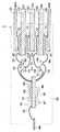
図4は、本実施形態に係る半導体装置を示した図である。図4(a)は、半導体装置2の平面図、図4(b)は半導体装置2の概略断面図である。また、図5は、図4(a)において各半導体素子11〜14の配置を模式的に示したものである。なお、図5では各リード101〜106を省略してある。また、図4(b)において、樹脂90の外壁部分は破線で示されており、この破線の内部に樹脂90が充填されている。 FIG. 4 is a diagram illustrating the semiconductor device according to the present embodiment. 4A is a plan view of the semiconductor device 2, and FIG. 4B is a schematic cross-sectional view of the semiconductor device 2. FIG. 5 schematically shows the arrangement of the
図4(a)に示されるように、本実施形態では、GND端子、M1、M2端子、そしてVdd端子、すなわち各リード101〜106が、同一平面上に配置された状態になっている。これら各リード101〜106は、図4(b)に示されるように、モールドパッケージ内で曲げ加工が施されている。これにより、樹脂90から露出した各リード101〜106の端部が同一平面上に配置されることとなる。 As shown in FIG. 4A, in the present embodiment, the GND terminal, M1, M2 terminal, and Vdd terminal, that is, the
具体的には、図4(b)、図5に示されるように、Vdd端子としてのリード101に第1半導体素子11のソースパッドが接合されている。また、リード101において第1半導体素子11が接合された面とは反対側の面に第3半導体素子13のソースパッド13aが接合されている。 Specifically, as shown in FIGS. 4B and 5, the source pad of the
上記第1半導体素子11のドレインパッドにM1端子としてのリード102が接合されており、リード102において第1半導体素子11が接合された面とは反対側の面に第2半導体素子12のドレインパッドが接合されている。このリード102において、第1、第2半導体素子11、12が接合された側とは反対側は、Vdd端子としてのリード101に対して多段構造にならないように曲げ加工が施されている。 A lead 102 as an M1 terminal is joined to the drain pad of the
そして、第2半導体素子12のソースパッド12aにGND端子としてのリード103が接合されている。このリード103においても、リード101、102に対して多段構造にならならないように曲げ加工が施されている。 A lead 103 as a GND terminal is bonded to the
同様に、第3半導体素子13のドレインパッドにM2端子としてのリード104が接合されており、リード104において第3半導体素子13が接合された面とは反対側の面に第4半導体素子14のドレインパッドが接合されている。そして、第4半導体素子14のソースパッドにGND端子としてのリード105が接合されている。これらリード104、105においても、上記と同様に、第3、第4半導体素子13、14が接合された側とは反対側がVdd端子としてのリード101に対してそれぞれ多段構造にならないように曲げ加工が施されている。 Similarly, the
さらに、リード102〜105の端部がリード101と同一平面内に配置されるようにリード102〜105がモールドパッケージ内で曲げ加工されている。これにより、各リード101〜106において樹脂90から露出する部分がそれぞれ同一平面上に配置される。また、上記のようにして各リード102〜105が曲げ加工される際、各リード101〜105がオーバーラップしないように、各半導体チップ11〜14から引き出され、樹脂90の外部まで引き伸ばされている。 Further, the
また、各半導体素子11〜14のゲートパッド11b〜14bにそれぞれワイヤ51〜54が接合されている。本実施形態では、図5に示されるように、各半導体素子11〜14が各リード101〜105の長手方向に垂直な方向にそれぞれ移動して配置されている。これにより、各半導体素子11〜14の各ゲートパッド11b〜14bから容易にワイヤ51〜54を引き伸ばすことができる。 Further,
なお、リード106は、M1、M2端子に接続されたモータMOによって駆動される窓ガラスの位置を検出するための位置検出用端子として用いられるものである。 The
以上のように、各半導体素子11〜14の配置のずれ、および各リード102〜105の曲げ加工によって、各リード101〜105が同一平面上に配置されるようにしても構わない。これにより、半導体装置2を外部に接続しやすい形態とすることができる。 As described above, the
(第3実施形態)
本実施形態では、上記実施形態と異なる部分についてのみ説明する。本実施形態では、各半導体素子11〜14に接合するVdd端子およびGND端子としての各リードの形状が上記実施形態と異なる。(Third embodiment)
In the present embodiment, only different portions from the above embodiment will be described. In this embodiment, the shape of each lead as a Vdd terminal and a GND terminal joined to each semiconductor element 11-14 differs from the said embodiment.
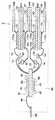
図6は、本実施形態に係る半導体装置の概略断面図である。また、図7は、図6のA矢視図である。なお、図6において、樹脂90の外壁部分は破線で示されており、この破線の内部に樹脂90が充填されている。また、図7では、リボンリード22、24、M1、M2端子(リード41〜44)、およびVdd端子(リード112)を省略してあるので、GND端子としてのリード111のみが描かれている。 FIG. 6 is a schematic cross-sectional view of the semiconductor device according to the present embodiment. FIG. 7 is a view taken in the direction of arrow A in FIG. In FIG. 6, the outer wall portion of the
図6に示されるように、本実施形態に係る半導体装置3では、紙面垂直方向、すなわちM1端子としてのリード41、42の長手方向に垂直な方向に各半導体素子11〜14がそれぞれ配置されている。図6では、第1、第2半導体素子11、12のみが描かれているが、上述のように、紙面垂直方向に図示されない第3、第4半導体素子13、14が配置されている。このような配置は、第2、第4半導体素子12、14に共通のGND端子と、第1、第3半導体素子11、13の共通のVdd端子と、を採用することで可能となる。 As shown in FIG. 6, in the
具体的には、図7に示されるように、リード111は、第2、第4半導体素子12、14が長手方向にそれぞれ接続される直線部位とその直線部位に垂直に配置された直線部位とで構成されるT字形状になっている。同様に、第1、第3半導体素子11、13が長手方向にそれぞれ接続される直線部位とその直線部位に垂直に配置された直線部位とで構成されるT字形状のリード112になっている。 Specifically, as shown in FIG. 7, the
そして、図6および図7に示されるように、GND端子としてのリード111に対して、リボンリード22、24を介して第2、第4半導体素子12、14の各ソースパッドが接続されている。また、GND端子と同じT字形状のVdd端子としてのリード112に対して、リボンリード21、23を介して第1、第3半導体素子11、13の各ソースパッドが接続されている。 As shown in FIGS. 6 and 7, the source pads of the second and
さらに、図6に示されるように、第1、第2半導体素子11、12の各ドレインパッドに接合された各リード41、42によってM1端子が構成されている。そして、図示しないが、第3、第4半導体素子13、14の各ドレインパッドに接合された各リード43、44によってM2端子が構成されている。 Furthermore, as shown in FIG. 6, the M1 terminal is configured by the
なお、各半導体素子11〜14の各ゲートパッド11b〜14bには、上記実施形態と同様に、ワイヤ51〜54が接続された状態になっている。 Note that the
以上のように、GND端子およびVdd端子としてのリード111、112をT字型にすることで、リード111、112の共通化を図るようにしても構わない。これにより、使用するリードの数を削減することができ、各半導体素子11〜14に対するリード41〜44、111、112の組み付けを容易に行うことができる。 As described above, the
(第4実施形態)
本実施形態では、上記実施形態と異なる部分についてのみ説明する。本実施形態では、M1端子としてのリード41、42、M2端子としてのリード43、44、およびVdd端子としてのリード31、33をそれぞれ1つのリードで構成したことが上記実施形態と異なる。(Fourth embodiment)
In the present embodiment, only different portions from the above embodiment will be described. This embodiment is different from the above embodiment in that the
図8は、本実施形態に係る半導体装置の概略断面図である。なお、図8において、樹脂90の外壁部分は破線で示されており、この破線の内部に樹脂90が充填されている。 FIG. 8 is a schematic cross-sectional view of the semiconductor device according to the present embodiment. In FIG. 8, the outer wall portion of the
図8に示されるように、本実施形態に係る半導体装置4では、Hブリッジ回路部分において、第2半導体素子12のドレインパッドにM1端子としてのリード121が接合されている。そして、リード121において第2半導体素子12が接合された面とは反対側の面に第1半導体素子11のドレインパッドが接合されている。 As shown in FIG. 8, in the
同様に、第4半導体素子14のドレインパッドにM2端子としてのリード122が接合されている。そして、リード122において第4半導体素子14が接合された面とは反対側の面に第3半導体素子13のドレインパッドが接合されている。また、第1、第3半導体素子11、13の各ソースパッドにリボンリード21、23を介してVdd端子としてのリード123がそれぞれ接続されている。 Similarly, a lead 122 as an M2 terminal is joined to the drain pad of the
以上のように、M1、M2端子およびVdd端子を共通のリード121〜123で構成することで、リード121〜123の構造を単純化させるようにしても構わない。これにより、M1、M2端子およびVdd端子を共通化することができ、半導体装置4の構成を簡略化することができる。 As described above, the structures of the
(第5実施形態)
本実施形態では、上記実施形態と異なる部分についてのみ説明する。本実施形態では、リボンリード21〜24を用いずに各半導体素子11〜14にGND端子、M1、M2端子、そしてVdd端子を接合していることが上記実施形態と異なる。また、第1、第3半導体素子11、13の各ゲートパッドと各中継リード61、63との間をリボンリードで接続していることが上記実施形態と異なる。(Fifth embodiment)
In the present embodiment, only different portions from the above embodiment will be described. The present embodiment is different from the above embodiment in that the GND terminals, M1, M2 terminals, and Vdd terminals are joined to the semiconductor elements 11-14 without using the ribbon leads 21-24. Further, the present embodiment is different from the above embodiment in that the gate pads of the first and
図9は、本実施形態に係る半導体装置の概略断面図である。なお、図9において、樹脂90の外壁部分は破線で示されており、この破線の内部に樹脂90が充填されている。 FIG. 9 is a schematic cross-sectional view of the semiconductor device according to the present embodiment. In FIG. 9, the outer wall portion of the
図9に示されるように、本実施形態に係る半導体装置5では、第2、第4半導体素子12、14の各ソースパッドにリード131、132の一端がそれぞれ接合されている。これらリード131、132の一端は、金属板の一端がリボンリードのように、圧延によって薄く引き伸ばされて曲げ加工されたリボンリード部131a、132aとされている。すなわち、第2、第4半導体素子の各ソースパッドに各リード131、132の各リボンリード部131a、132aが直接接合されている。また、各リード131、132の他端は、それぞれGND端子として樹脂90から露出した状態になっている。 As shown in FIG. 9, in the
同様に、第1、第3半導体素子11、13の各ソースパッドにリード133、134のリボンリード部133a、134aがそれぞれ直接接合されている。これらリード133、134は上記各リード131、132と同様の形状をなしている。そして、各リード133、134の他端がそれぞれ張り合わされてVdd端子として樹脂90から露出した状態になっている。 Similarly, the
また、第1、第3半導体素子11、13の各ゲートパッドと中継リード61、62との間は、リボンリード151、152でそれぞれ接続されている。これにより、リード133、134を第1、第3半導体素子11、13にそれぞれ接合する際に、上記リボンリード151、152をそれぞれ各ゲートパッドと中継リード61、62との間に接続できる。このため、第2、第4半導体素子12、14と各中継リード62、64との間をワイヤボンドすれば良いので、半導体装置5の製造を容易にすることができる。 The gate pads of the first and
以上のように、各半導体素子11〜14の各ソースパッドに各リード131〜134の各リボンリード部131a〜134aを直接接合させるようにしても構わない。これにより、各半導体素子11〜14で発生した熱を、各半導体素子11〜14にそれぞれ直接接合されたリード41〜44、131〜134を介して放熱することができる。 As described above, the
なお、本実施形態で用いられたリード131〜134は、本発明の加工リードに相当する。 The leads 131 to 134 used in this embodiment correspond to the processed leads of the present invention.
(他の実施形態)
上記各実施形態で示された構造、形態は一例を示すものであって、各実施形態で示された内容をそれぞれ組み合わせて実施しても構わない。(Other embodiments)
The structures and forms shown in the above embodiments are examples, and the contents shown in the embodiments may be combined.
上記各実施形態では、各半導体素子11〜14と積層基板81内の電気回路との間をそれぞれ1つの中継リード61〜64を介して電気的に接続しているが、それぞれ複数の中継リードを介すようにしても構わない。 In each of the above embodiments, each of the
上記各実施形態において、各半導体装置1〜5の各GND端子をモータMOの筐体へ接続し、GND端子からモータMOの筐体へ直接放熱するようにしても構わない。これにより、リード平面から放熱できるので効率がよい。 In the above embodiments, the GND terminals of the
上記第3実施形態において、M1端子を構成する各リード41、42を共通化させて1本のリードで構成しても構わない。同様に、第5実施形態において、M1、M2端子およびVdd端子を構成する各リード41〜44、133、134をそれぞれ共通のリードで構成するようにしても構わない。 In the third embodiment, each of the
また、第5実施形態のように第1、第3半導体チップ11、13と中継リード61、63とをリボンリード151、152で接続する形態を、例えば第1、2、4実施形態にそれぞれ適用させても構わない。 Further, the configuration in which the first and
上記第2実施形態と同様に、第1、第3〜第5実施形態においても、各リード31〜34、41〜44、111、112、121〜123、131〜134を樹脂90内でそれぞれ曲げ加工することにより、樹脂90から露出する部分をそれぞれ同一平面上に配置させるようにしても構わない。 Similarly to the second embodiment, in the first, third to fifth embodiments, the
上記各実施形態では、各半導体素子11〜14としてパワー素子を用いているが、他の例としてIGBTやバイポーラパワー素子を用いても構わない。 In each said embodiment, although the power element is used as each semiconductor element 11-14, you may use IGBT and a bipolar power element as another example.
また、放熱性向上のため、図1および図8に示される各リード32、34、図4(b)に示される各リード103、105、そして図6に示される各リード111、112を樹脂90からそれぞれ露出させるようにしても良い。 Further, in order to improve heat dissipation, the
11〜14…第1〜第4半導体素子、21〜24…リボンリード、31〜34、41〜44、101〜105、111、112、121〜123、131〜134…リード、131a〜134a…リボンリード部、51〜54、71〜74…ワイヤ、61〜64…中継リード、81…積層基板、82…電子素子としての駆動用チップ、85…電子素子としてのマイコンチップ、90…樹脂。 11-14 ... 1st-4th semiconductor element, 21-24 ... Ribbon lead, 31-34, 41-44, 101-105, 111, 112, 121-123, 131-134 ... Lead, 131a-134a ... Ribbon Lead part, 51-54, 71-74 ... wire, 61-64 ... relay lead, 81 ... laminated substrate, 82 ... driving chip as electronic element, 85 ... microcomputer chip as electronic element, 90 ... resin.
Claims (14)
Translated fromJapanese電気回路が形成された基板(81)上に設けられると共に、前記電気回路を介して前記各半導体素子を駆動制御する電子素子(82、85)と、
配線およびヒートシンクとしての金属リード(21〜24、31〜34、41〜44、101〜105、111、112、121〜123、131〜134)と、
前記各半導体素子および前記金属リードの一端側を封止した樹脂(90)と、を備えた半導体装置であって、
前記各半導体素子は積層状に配置されると共に、Hブリッジ状に接続された構成とされており、
前記各半導体素子の各第1電極および各第2電極それぞれに前記金属リードがそれぞれ直接接合されており、前記各半導体素子で発生した熱は、前記金属リードを介してそれぞれ放熱されるようになっていることを特徴とする半導体装置。Four vertical first to fourth semiconductor elements (11 to 14) configured to allow current to flow between a first electrode formed on the front surface side of the semiconductor substrate and a second electrode formed on the back surface. When,
An electronic element (82, 85) provided on a substrate (81) on which an electric circuit is formed, and driving and controlling each of the semiconductor elements via the electric circuit;
Metal leads (21-24, 31-34, 41-44, 101-105, 111, 112, 121-123, 131-134) as wiring and heat sinks;
A semiconductor device comprising a resin (90) that seals one end side of each of the semiconductor elements and the metal lead,
Each of the semiconductor elements is arranged in a stacked manner and connected in an H-bridge shape,
The metal leads are directly joined to the first electrodes and the second electrodes of the semiconductor elements, respectively, and the heat generated in the semiconductor elements is radiated through the metal leads. A semiconductor device characterized by that.
前記各半導体素子の各第1電極に前記リボンリード(21〜24)のうちの一部がそれぞれ直接接合されると共に、前記リボンリードのうち前記各半導体素子の各第1電極に接合されていない部分の一部が板状リード(31〜34、111、112、123)に接合され、前記リボンリードが接合された前記板状リードとは別の板状リード(41〜44、121、122)が前記各半導体素子の各第2電極にそれぞれ直接接合されていることを特徴とする請求項1ないし3のいずれか1つに記載の半導体装置。The metal lead is composed of a plurality of plate-like leads (31-34, 41-44, 111, 112, 121-123) and ribbon leads (21-24) thinner than the plate-like leads. ,
A part of the ribbon leads (21 to 24) is directly bonded to the first electrodes of the semiconductor elements, and is not bonded to the first electrodes of the semiconductor elements of the ribbon leads. Part of the portion is joined to plate-like leads (31-34, 111, 112, 123), and plate-like leads (41-44, 121, 122) different from the plate-like leads to which the ribbon leads are joined. The semiconductor device according to claim 1, wherein the semiconductor device is directly bonded to each second electrode of each semiconductor element.
前記第1〜第4半導体素子の各第2電極にそれぞれ接合された前記各板状リード(41〜44)のうち、前記第1および第2半導体素子(11、12)が接合された各板状リード(41、42)が、前記第1および第2半導体素子が接合された面とは反対側の面が互いに張り合わされると共に、前記第3および第4半導体素子(13、14)が接合された板状リード(43、44)が、前記第3および第4半導体素子が接合された面とは反対側の面が互いに張り合わされることでそれぞれ負荷接続用端子(M1、M2)が構成され、
前記リボンリード(22、24)を介して前記第2および第4半導体素子(12、14)の各第1電極にそれぞれ接続された前記各板状リード(32、34)がそれぞれ接地用端子(GND)として構成されていることを特徴とする請求項4に記載の半導体装置。The plate-like leads (31, 33) connected to the first electrodes of the first and third semiconductor elements (11, 13) via the ribbon leads (21, 23), respectively, A power supply terminal (Vdd) is configured by bonding surfaces opposite to the surface to which the third semiconductor element is bonded to each other.
Of the plate-like leads (41 to 44) joined to the second electrodes of the first to fourth semiconductor elements, the plates to which the first and second semiconductor elements (11, 12) are joined. The surface leads opposite to the surface where the first and second semiconductor elements are bonded are bonded to each other, and the third and fourth semiconductor elements (13, 14) are bonded to each other. Loaded terminals (M1, M2) are formed by bonding the plate-like leads (43, 44) to the surfaces opposite to the surfaces where the third and fourth semiconductor elements are joined to each other. And
The plate-like leads (32, 34) connected to the first electrodes of the second and fourth semiconductor elements (12, 14) via the ribbon leads (22, 24) are respectively connected to ground terminals ( The semiconductor device according to claim 4, wherein the semiconductor device is configured as GND).
前記リボンリード(21、23)を介して前記第1および第3半導体素子(11、13)の各第1電極にそれぞれ共通の板状リード(112)が接続されることで、前記第1および第3半導体素子が横並びに配置されており、
前記第1および第3半導体素子それぞれに対応した前記第2および第4半導体素子の各第1電極に前記リボンリード(22、24)を介してそれぞれ共通の板状リード(111)が接続されることで、前記第2および第4半導体素子が横並びに配置されていることを特徴とする請求項4に記載の半導体装置。Among the plate-like leads (41 to 44) respectively joined to the second electrodes of the semiconductor elements, the plate-like leads (41, 41) to which the first and second semiconductor elements (11, 12) are joined. 42), each of the plate-like shapes in which the surfaces opposite to the surface where the first and second semiconductor elements are bonded are bonded together and the third and fourth semiconductor elements (13, 14) are bonded together. The leads (43, 44) are bonded to each other on the surface opposite to the surface on which the third and fourth semiconductor elements are joined to form load connection terminals (M1, M2), respectively.
A common plate-like lead (112) is connected to each first electrode of the first and third semiconductor elements (11, 13) via the ribbon lead (21, 23). The third semiconductor elements are arranged side by side;
A common plate-like lead (111) is connected to each first electrode of the second and fourth semiconductor elements corresponding to each of the first and third semiconductor elements via the ribbon leads (22, 24). The semiconductor device according to claim 4, wherein the second and fourth semiconductor elements are arranged side by side.
前記第2および第4半導体素子がそれぞれ接続される共通の板状リード(111)は、前記第2および第4半導体素子が長手方向にそれぞれ接続される直線部位とその直線部位に垂直に配置された直線部位とで構成されるT字形状になっていることを特徴とする請求項6に記載の半導体装置。The common plate-like lead (112) to which the first and third semiconductor elements are respectively connected is disposed in a straight line portion where the first and third semiconductor elements are connected in the longitudinal direction and perpendicular to the straight line portion. It has a T-shape composed of straight parts
The common plate-like lead (111) to which the second and fourth semiconductor elements are respectively connected is disposed perpendicular to the straight part and the straight part to which the second and fourth semiconductor elements are connected in the longitudinal direction. The semiconductor device according to claim 6, wherein the semiconductor device has a T-shape composed of a straight portion.
前記板状リードが張り合わされたとき、一方の板状リードに設けられた凹部に他方の板状リードに設けられた凸部が嵌合するようになっていることを特徴とする請求項5ないし7のいずれか1つに記載の半導体装置。In the plate-like leads (31, 33, 41 to 44) bonded to each other, a concave portion is provided on one of the surfaces bonded to each other, and a convex portion corresponding to the concave portion is provided on the other side.
6. A projection provided on the other plate-like lead is fitted into a depression provided on one plate-like lead when the plate-like leads are bonded together. 8. The semiconductor device according to any one of 7.
前記第2半導体素子の第2電極に直接接合された板状リード(102、121)が第1負荷接続用端子(M1)として構成されると共に、前記第2半導体素子が接合された板状リード(102、121)が、前記第2半導体素子が接合された面とは反対側の面に第1半導体素子(11)の第2電極が直接接合されており、
前記第1半導体素子の第1電極にリボンリード(21)を介して接続された板状リード(101、123)が電源端子(Vdd)として構成されると共に、前記第1半導体素子が接続された板状リード(101、123)が、前記第1半導体素子が接続された面とは反対側の面にリボンリード(23)を介して第3半導体素子(13)の第1電極が接続され、前記第3半導体素子の第2電極に直接接合された板状リード(104、122)が第2負荷接続用端子(M2)として構成されており、
前記第3半導体素子の第2電極が接合された板状リード(104、122)が、前記第3半導体素子が接合された面とは反対側の面に第4半導体素子(14)の第2電極が直接接合されると共に、前記第4半導体素子の第1電極にリボンリード(24)を介して接続された板状リード(34、105)が接地用端子(GND)として構成されていることを特徴とする請求項4に記載の半導体装置。Plate-like leads (32, 103) connected to the first electrode of the second semiconductor element (12) via the ribbon lead (22) are configured as ground terminals (GND),
Plate-like leads (102, 121) directly joined to the second electrode of the second semiconductor element are configured as first load connection terminals (M1), and plate-like leads to which the second semiconductor element is joined. (102, 121), the second electrode of the first semiconductor element (11) is directly bonded to the surface opposite to the surface to which the second semiconductor element is bonded;
Plate-shaped leads (101, 123) connected to the first electrode of the first semiconductor element via ribbon leads (21) are configured as power supply terminals (Vdd), and the first semiconductor element is connected. The plate-like leads (101, 123) are connected to the first electrode of the third semiconductor element (13) via the ribbon lead (23) on the surface opposite to the surface to which the first semiconductor element is connected, Plate-like leads (104, 122) directly joined to the second electrode of the third semiconductor element are configured as second load connection terminals (M2),
The plate-like leads (104, 122) to which the second electrode of the third semiconductor element is bonded have the second side of the fourth semiconductor element (14) on the surface opposite to the surface to which the third semiconductor element is bonded. The electrodes are directly joined, and plate-like leads (34, 105) connected to the first electrode of the fourth semiconductor element via the ribbon lead (24) are configured as ground terminals (GND). The semiconductor device according to claim 4.
前記各半導体素子の各第1電極に前記加工リードのリボンリード部がそれぞれ直接接合されると共に、前記各板状リードが前記各半導体素子の各第2電極にそれぞれ直接接合されていることを特徴とする請求項1ないし3のいずれか1つに記載の半導体装置。The metal lead is composed of processing leads (131 to 134) and plate-like leads (41 to 44) provided with ribbon lead portions (131a to 134a) in which one end side of the metal plate is thinned,
Ribbon lead portions of the processing leads are directly bonded to the first electrodes of the semiconductor elements, respectively, and the plate-like leads are directly bonded to the second electrodes of the semiconductor elements. The semiconductor device according to claim 1.
前記第1〜第4半導体素子の各第2電極にそれぞれ接合された各板状リード(41〜44)のうち、前記第1および第2半導体素子(11、12)が接合された板状リード(41、42)が、前記第1および第2半導体素子が接合された面とは反対側の面が互いに張り合わされ、
前記第3および第4半導体素子(13、14)が接合された板状リード(43、44)が、前記第3および第4半導体素子が接合された面とは反対側の面が互いに張り合わされることでそれぞれ負荷接続用端子(M1、M2)が構成されており、
前記第2および第4半導体素子(12、14)の各第1電極にリボンリード部(131a、132a)がそれぞれ直接接合された各加工リード(131、132)が、それぞれ接地用端子(GND)として構成されていることを特徴とする請求項11に記載の半導体装置。The processed leads (133, 134) in which ribbon lead portions (133a, 134a) are directly joined to the first electrodes of the first and third semiconductor elements (11, 13) are respectively connected to the first and third semiconductors. The power supply terminal (Vdd) is configured by sticking the surfaces opposite to the surface where the elements are bonded together,
Of the plate-like leads (41 to 44) respectively joined to the second electrodes of the first to fourth semiconductor elements, the plate-like leads to which the first and second semiconductor elements (11, 12) are joined. (41, 42) are bonded to each other on the surface opposite to the surface on which the first and second semiconductor elements are joined,
The plate-like leads (43, 44) to which the third and fourth semiconductor elements (13, 14) are joined are bonded to each other on the surface opposite to the face to which the third and fourth semiconductor elements are joined. Thus, the load connection terminals (M1, M2) are configured respectively.
The processing leads (131, 132) in which the ribbon lead portions (131a, 132a) are directly bonded to the first electrodes of the second and fourth semiconductor elements (12, 14) are ground terminals (GND), respectively. The semiconductor device according to claim 11, wherein the semiconductor device is configured as follows.
前記板状リードが張り合わされたとき、一方の板状リードに設けられた凹部に他方の板状リードに設けられた凸部が嵌合するようになっていることを特徴とする請求項12または13に記載の半導体装置。In the plate-like leads (41 to 44) and the processed leads (133, 134) that are attached to each other, a concave portion is provided on one of the surfaces that are attached to each other, and a convex portion that corresponds to the concave portion is provided on the other side. And
The projecting portion provided on the other plate-like lead is fitted into the recess provided on one of the plate-like leads when the plate-like leads are bonded to each other. 14. The semiconductor device according to 13.
Priority Applications (2)
| Application Number | Priority Date | Filing Date | Title |
|---|---|---|---|
| JP2005257822AJP4552810B2 (en) | 2005-09-06 | 2005-09-06 | Semiconductor device |
| US11/515,045US20070075419A1 (en) | 2005-09-06 | 2006-09-05 | Semiconductor device having metallic lead and electronic device having lead frame |
Applications Claiming Priority (1)
| Application Number | Priority Date | Filing Date | Title |
|---|---|---|---|
| JP2005257822AJP4552810B2 (en) | 2005-09-06 | 2005-09-06 | Semiconductor device |
Publications (2)
| Publication Number | Publication Date |
|---|---|
| JP2007073674A JP2007073674A (en) | 2007-03-22 |
| JP4552810B2true JP4552810B2 (en) | 2010-09-29 |
Family
ID=37934879
Family Applications (1)
| Application Number | Title | Priority Date | Filing Date |
|---|---|---|---|
| JP2005257822AExpired - Fee RelatedJP4552810B2 (en) | 2005-09-06 | 2005-09-06 | Semiconductor device |
Country Status (1)
| Country | Link |
|---|---|
| JP (1) | JP4552810B2 (en) |
Families Citing this family (7)
| Publication number | Priority date | Publication date | Assignee | Title |
|---|---|---|---|---|
| JP4600576B2 (en) | 2008-05-08 | 2010-12-15 | 株式会社デンソー | Semiconductor device and manufacturing method thereof |
| JP2011108946A (en)* | 2009-11-19 | 2011-06-02 | Aisin Seiki Co Ltd | Method of mounting transistor, and electronic component |
| JP5600931B2 (en)* | 2009-12-11 | 2014-10-08 | 株式会社豊田中央研究所 | Power converter |
| JP2011134990A (en) | 2009-12-25 | 2011-07-07 | Renesas Electronics Corp | Semiconductor device and manufacturing method therefor |
| JP2013191788A (en) | 2012-03-15 | 2013-09-26 | Denso Corp | Semiconductor module and semiconductor device |
| DE102014209690B4 (en)* | 2014-05-21 | 2020-02-20 | Robert Bosch Gmbh | Kommutierungszelle |
| JP6598739B2 (en)* | 2016-07-14 | 2019-10-30 | 三菱電機株式会社 | Semiconductor module |
Family Cites Families (4)
| Publication number | Priority date | Publication date | Assignee | Title |
|---|---|---|---|---|
| JP2002026251A (en)* | 2000-07-11 | 2002-01-25 | Toshiba Corp | Semiconductor device |
| JP2002208673A (en)* | 2001-01-10 | 2002-07-26 | Mitsubishi Electric Corp | Semiconductor device and power module |
| JP4239580B2 (en)* | 2002-12-13 | 2009-03-18 | 株式会社デンソー | Semiconductor device |
| JP4196001B2 (en)* | 2004-02-17 | 2008-12-17 | パナソニック株式会社 | Semiconductor power module |
- 2005
- 2005-09-06JPJP2005257822Apatent/JP4552810B2/ennot_activeExpired - Fee Related
Also Published As
| Publication number | Publication date |
|---|---|
| JP2007073674A (en) | 2007-03-22 |
Similar Documents
| Publication | Publication Date | Title |
|---|---|---|
| CN108364942B (en) | Semiconductor device with a plurality of transistors | |
| US20070075419A1 (en) | Semiconductor device having metallic lead and electronic device having lead frame | |
| JP4438489B2 (en) | Semiconductor device | |
| CN114175234B (en) | Semiconductor devices and electronic devices | |
| CN110178219B (en) | Semiconductor device and power conversion device | |
| JP6619356B2 (en) | Power semiconductor device and manufacturing method thereof | |
| JP5381444B2 (en) | Power module | |
| JP2009534869A (en) | Semiconductor die package including multiple die and common node structure | |
| CN101419964A (en) | Device with a plurality of semiconductor chips | |
| CN205039149U (en) | Semiconductor device | |
| CN110785838A (en) | Resin encapsulated power semiconductor module with exposed terminal areas | |
| CN113169161A (en) | Semiconductor package, method for manufacturing the same, and semiconductor device | |
| WO2021200337A1 (en) | Electronic device | |
| WO2021251126A1 (en) | Semiconductor device | |
| CN103972277A (en) | Semiconductor device and method of manufacturing the same | |
| CN110447094A (en) | Semiconductor device, method for manufacturing the same, and power conversion device | |
| JP4552810B2 (en) | Semiconductor device | |
| JP2008218688A (en) | Semiconductor device | |
| JP2009141150A (en) | Semiconductor device | |
| US9837386B2 (en) | Power device and preparation method thereof | |
| JP5257229B2 (en) | Semiconductor device and heat sink | |
| JP2005277014A (en) | Semiconductor device | |
| KR20170069322A (en) | Power module | |
| JP6371122B2 (en) | Power semiconductor device and resin-sealed motor | |
| WO2024247629A1 (en) | Semiconductor device and vehicle |
Legal Events
| Date | Code | Title | Description |
|---|---|---|---|
| A621 | Written request for application examination | Free format text:JAPANESE INTERMEDIATE CODE: A621 Effective date:20070918 | |
| A977 | Report on retrieval | Free format text:JAPANESE INTERMEDIATE CODE: A971007 Effective date:20080130 | |
| TRDD | Decision of grant or rejection written | ||
| A01 | Written decision to grant a patent or to grant a registration (utility model) | Free format text:JAPANESE INTERMEDIATE CODE: A01 Effective date:20100622 | |
| A01 | Written decision to grant a patent or to grant a registration (utility model) | Free format text:JAPANESE INTERMEDIATE CODE: A01 | |
| A61 | First payment of annual fees (during grant procedure) | Free format text:JAPANESE INTERMEDIATE CODE: A61 Effective date:20100705 | |
| FPAY | Renewal fee payment (event date is renewal date of database) | Free format text:PAYMENT UNTIL: 20130723 Year of fee payment:3 | |
| FPAY | Renewal fee payment (event date is renewal date of database) | Free format text:PAYMENT UNTIL: 20130723 Year of fee payment:3 | |
| R250 | Receipt of annual fees | Free format text:JAPANESE INTERMEDIATE CODE: R250 | |
| R250 | Receipt of annual fees | Free format text:JAPANESE INTERMEDIATE CODE: R250 | |
| LAPS | Cancellation because of no payment of annual fees |