JP4551045B2 - A method of producing a polycrystalline thin film semiconductor having uniform and large crystal grains and manipulating grain boundary positions using continuous lateral solidification. - Google Patents
A method of producing a polycrystalline thin film semiconductor having uniform and large crystal grains and manipulating grain boundary positions using continuous lateral solidification.Download PDFInfo
- Publication number
- JP4551045B2 JP4551045B2JP2001522579AJP2001522579AJP4551045B2JP 4551045 B2JP4551045 B2JP 4551045B2JP 2001522579 AJP2001522579 AJP 2001522579AJP 2001522579 AJP2001522579 AJP 2001522579AJP 4551045 B2JP4551045 B2JP 4551045B2
- Authority
- JP
- Japan
- Prior art keywords
- thin film
- silicon
- laser
- mask
- region
- Prior art date
- Legal status (The legal status is an assumption and is not a legal conclusion. Google has not performed a legal analysis and makes no representation as to the accuracy of the status listed.)
- Expired - Fee Related
Links
- 239000010409thin filmSubstances0.000titleclaimsdescription83
- 238000000034methodMethods0.000titleclaimsdescription75
- 239000013078crystalSubstances0.000titleclaimsdescription38
- 239000004065semiconductorSubstances0.000titledescription11
- 238000007711solidificationMethods0.000titledescription11
- 230000008023solidificationEffects0.000titledescription11
- XUIMIQQOPSSXEZ-UHFFFAOYSA-NSiliconChemical compound[Si]XUIMIQQOPSSXEZ-UHFFFAOYSA-N0.000claimsdescription68
- 229910052710siliconInorganic materials0.000claimsdescription66
- 239000010703siliconSubstances0.000claimsdescription66
- 229910021420polycrystalline siliconInorganic materials0.000claimsdescription38
- 239000010408filmSubstances0.000claimsdescription37
- 230000000873masking effectEffects0.000claimsdescription27
- 239000011856silicon-based particleSubstances0.000claimsdescription23
- 229910021417amorphous siliconInorganic materials0.000claimsdescription18
- 238000000926separation methodMethods0.000claimsdescription16
- 230000008018meltingEffects0.000claimsdescription15
- 238000002844meltingMethods0.000claimsdescription15
- 239000002245particleSubstances0.000claimsdescription12
- 238000012545processingMethods0.000claimsdescription12
- 230000001678irradiating effectEffects0.000claimsdescription7
- 230000006911nucleationEffects0.000claimsdescription7
- 238000010899nucleationMethods0.000claimsdescription7
- 239000000758substrateSubstances0.000claimsdescription6
- 239000000155meltSubstances0.000claimsdescription4
- 230000006698inductionEffects0.000claimsdescription2
- 238000000137annealingMethods0.000claims11
- 238000005192partitionMethods0.000claims1
- 238000010586diagramMethods0.000description16
- 238000004519manufacturing processMethods0.000description7
- 241000280258Dyschoriste linearisSpecies0.000description5
- 239000010432diamondSubstances0.000description4
- 229910003460diamondInorganic materials0.000description4
- 230000015572biosynthetic processEffects0.000description2
- 229910021419crystalline siliconInorganic materials0.000description2
- 238000002425crystallisationMethods0.000description2
- 230000008025crystallizationEffects0.000description2
- 238000005224laser annealingMethods0.000description2
- 229910021421monocrystalline siliconInorganic materials0.000description2
- 230000003287optical effectEffects0.000description2
- 238000003672processing methodMethods0.000description2
- 238000012546transferMethods0.000description2
- 239000011248coating agentSubstances0.000description1
- 238000000576coating methodMethods0.000description1
- 238000004320controlled atmosphereMethods0.000description1
- 238000007796conventional methodMethods0.000description1
- 230000007423decreaseEffects0.000description1
- 239000010438graniteSubstances0.000description1
- 239000004973liquid crystal related substanceSubstances0.000description1
- 239000011159matrix materialSubstances0.000description1
- 239000002184metalSubstances0.000description1
- 238000012986modificationMethods0.000description1
- 230000004048modificationEffects0.000description1
- 229920005591polysiliconPolymers0.000description1
- 239000010453quartzSubstances0.000description1
- VYPSYNLAJGMNEJ-UHFFFAOYSA-Nsilicon dioxideInorganic materialsO=[Si]=OVYPSYNLAJGMNEJ-UHFFFAOYSA-N0.000description1
Images


Classifications
- B—PERFORMING OPERATIONS; TRANSPORTING
- B23—MACHINE TOOLS; METAL-WORKING NOT OTHERWISE PROVIDED FOR
- B23K—SOLDERING OR UNSOLDERING; WELDING; CLADDING OR PLATING BY SOLDERING OR WELDING; CUTTING BY APPLYING HEAT LOCALLY, e.g. FLAME CUTTING; WORKING BY LASER BEAM
- B23K26/00—Working by laser beam, e.g. welding, cutting or boring
- B23K26/02—Positioning or observing the workpiece, e.g. with respect to the point of impact; Aligning, aiming or focusing the laser beam
- B23K26/06—Shaping the laser beam, e.g. by masks or multi-focusing
- B23K26/062—Shaping the laser beam, e.g. by masks or multi-focusing by direct control of the laser beam
- B23K26/0622—Shaping the laser beam, e.g. by masks or multi-focusing by direct control of the laser beam by shaping pulses
- B—PERFORMING OPERATIONS; TRANSPORTING
- B23—MACHINE TOOLS; METAL-WORKING NOT OTHERWISE PROVIDED FOR
- B23K—SOLDERING OR UNSOLDERING; WELDING; CLADDING OR PLATING BY SOLDERING OR WELDING; CUTTING BY APPLYING HEAT LOCALLY, e.g. FLAME CUTTING; WORKING BY LASER BEAM
- B23K26/00—Working by laser beam, e.g. welding, cutting or boring
- B23K26/02—Positioning or observing the workpiece, e.g. with respect to the point of impact; Aligning, aiming or focusing the laser beam
- B23K26/06—Shaping the laser beam, e.g. by masks or multi-focusing
- B23K26/062—Shaping the laser beam, e.g. by masks or multi-focusing by direct control of the laser beam
- B23K26/0626—Energy control of the laser beam
- B—PERFORMING OPERATIONS; TRANSPORTING
- B23—MACHINE TOOLS; METAL-WORKING NOT OTHERWISE PROVIDED FOR
- B23K—SOLDERING OR UNSOLDERING; WELDING; CLADDING OR PLATING BY SOLDERING OR WELDING; CUTTING BY APPLYING HEAT LOCALLY, e.g. FLAME CUTTING; WORKING BY LASER BEAM
- B23K26/00—Working by laser beam, e.g. welding, cutting or boring
- B23K26/02—Positioning or observing the workpiece, e.g. with respect to the point of impact; Aligning, aiming or focusing the laser beam
- B23K26/06—Shaping the laser beam, e.g. by masks or multi-focusing
- B23K26/064—Shaping the laser beam, e.g. by masks or multi-focusing by means of optical elements, e.g. lenses, mirrors or prisms
- B23K26/066—Shaping the laser beam, e.g. by masks or multi-focusing by means of optical elements, e.g. lenses, mirrors or prisms by using masks
- G—PHYSICS
- G03—PHOTOGRAPHY; CINEMATOGRAPHY; ANALOGOUS TECHNIQUES USING WAVES OTHER THAN OPTICAL WAVES; ELECTROGRAPHY; HOLOGRAPHY
- G03F—PHOTOMECHANICAL PRODUCTION OF TEXTURED OR PATTERNED SURFACES, e.g. FOR PRINTING, FOR PROCESSING OF SEMICONDUCTOR DEVICES; MATERIALS THEREFOR; ORIGINALS THEREFOR; APPARATUS SPECIALLY ADAPTED THEREFOR
- G03F7/00—Photomechanical, e.g. photolithographic, production of textured or patterned surfaces, e.g. printing surfaces; Materials therefor, e.g. comprising photoresists; Apparatus specially adapted therefor
- G03F7/70—Microphotolithographic exposure; Apparatus therefor
- G03F7/70008—Production of exposure light, i.e. light sources
- G03F7/70041—Production of exposure light, i.e. light sources by pulsed sources, e.g. multiplexing, pulse duration, interval control or intensity control
- G—PHYSICS
- G03—PHOTOGRAPHY; CINEMATOGRAPHY; ANALOGOUS TECHNIQUES USING WAVES OTHER THAN OPTICAL WAVES; ELECTROGRAPHY; HOLOGRAPHY
- G03F—PHOTOMECHANICAL PRODUCTION OF TEXTURED OR PATTERNED SURFACES, e.g. FOR PRINTING, FOR PROCESSING OF SEMICONDUCTOR DEVICES; MATERIALS THEREFOR; ORIGINALS THEREFOR; APPARATUS SPECIALLY ADAPTED THEREFOR
- G03F7/00—Photomechanical, e.g. photolithographic, production of textured or patterned surfaces, e.g. printing surfaces; Materials therefor, e.g. comprising photoresists; Apparatus specially adapted therefor
- G03F7/70—Microphotolithographic exposure; Apparatus therefor
- G03F7/70691—Handling of masks or workpieces
- G03F7/70716—Stages
- G03F7/70725—Stages control
- H—ELECTRICITY
- H01—ELECTRIC ELEMENTS
- H01L—SEMICONDUCTOR DEVICES NOT COVERED BY CLASS H10
- H01L21/00—Processes or apparatus adapted for the manufacture or treatment of semiconductor or solid state devices or of parts thereof
- H01L21/02—Manufacture or treatment of semiconductor devices or of parts thereof
- H01L21/02104—Forming layers
- H01L21/02365—Forming inorganic semiconducting materials on a substrate
- H01L21/02518—Deposited layers
- H01L21/02521—Materials
- H01L21/02524—Group 14 semiconducting materials
- H01L21/02532—Silicon, silicon germanium, germanium
- H—ELECTRICITY
- H01—ELECTRIC ELEMENTS
- H01L—SEMICONDUCTOR DEVICES NOT COVERED BY CLASS H10
- H01L21/00—Processes or apparatus adapted for the manufacture or treatment of semiconductor or solid state devices or of parts thereof
- H01L21/02—Manufacture or treatment of semiconductor devices or of parts thereof
- H01L21/02104—Forming layers
- H01L21/02365—Forming inorganic semiconducting materials on a substrate
- H01L21/02656—Special treatments
- H01L21/02664—Aftertreatments
- H01L21/02667—Crystallisation or recrystallisation of non-monocrystalline semiconductor materials, e.g. regrowth
- H01L21/02675—Crystallisation or recrystallisation of non-monocrystalline semiconductor materials, e.g. regrowth using laser beams
- H01L21/02678—Beam shaping, e.g. using a mask
- H01L21/0268—Shape of mask
- H—ELECTRICITY
- H01—ELECTRIC ELEMENTS
- H01L—SEMICONDUCTOR DEVICES NOT COVERED BY CLASS H10
- H01L21/00—Processes or apparatus adapted for the manufacture or treatment of semiconductor or solid state devices or of parts thereof
- H01L21/02—Manufacture or treatment of semiconductor devices or of parts thereof
- H01L21/02104—Forming layers
- H01L21/02365—Forming inorganic semiconducting materials on a substrate
- H01L21/02656—Special treatments
- H01L21/02664—Aftertreatments
- H01L21/02667—Crystallisation or recrystallisation of non-monocrystalline semiconductor materials, e.g. regrowth
- H01L21/02675—Crystallisation or recrystallisation of non-monocrystalline semiconductor materials, e.g. regrowth using laser beams
- H01L21/02686—Pulsed laser beam
- H—ELECTRICITY
- H01—ELECTRIC ELEMENTS
- H01L—SEMICONDUCTOR DEVICES NOT COVERED BY CLASS H10
- H01L21/00—Processes or apparatus adapted for the manufacture or treatment of semiconductor or solid state devices or of parts thereof
- H01L21/02—Manufacture or treatment of semiconductor devices or of parts thereof
- H01L21/02104—Forming layers
- H01L21/02365—Forming inorganic semiconducting materials on a substrate
- H01L21/02656—Special treatments
- H01L21/02664—Aftertreatments
- H01L21/02667—Crystallisation or recrystallisation of non-monocrystalline semiconductor materials, e.g. regrowth
- H01L21/02691—Scanning of a beam
- H—ELECTRICITY
- H10—SEMICONDUCTOR DEVICES; ELECTRIC SOLID-STATE DEVICES NOT OTHERWISE PROVIDED FOR
- H10D—INORGANIC ELECTRIC SEMICONDUCTOR DEVICES
- H10D62/00—Semiconductor bodies, or regions thereof, of devices having potential barriers
- H10D62/40—Crystalline structures
- H—ELECTRICITY
- H10—SEMICONDUCTOR DEVICES; ELECTRIC SOLID-STATE DEVICES NOT OTHERWISE PROVIDED FOR
- H10D—INORGANIC ELECTRIC SEMICONDUCTOR DEVICES
- H10D86/00—Integrated devices formed in or on insulating or conducting substrates, e.g. formed in silicon-on-insulator [SOI] substrates or on stainless steel or glass substrates
- H10D86/01—Manufacture or treatment
- H10D86/021—Manufacture or treatment of multiple TFTs
- H10D86/0221—Manufacture or treatment of multiple TFTs comprising manufacture, treatment or patterning of TFT semiconductor bodies
- H10D86/0223—Manufacture or treatment of multiple TFTs comprising manufacture, treatment or patterning of TFT semiconductor bodies comprising crystallisation of amorphous, microcrystalline or polycrystalline semiconductor materials
- H10D86/0229—Manufacture or treatment of multiple TFTs comprising manufacture, treatment or patterning of TFT semiconductor bodies comprising crystallisation of amorphous, microcrystalline or polycrystalline semiconductor materials characterised by control of the annealing or irradiation parameters
- H—ELECTRICITY
- H10—SEMICONDUCTOR DEVICES; ELECTRIC SOLID-STATE DEVICES NOT OTHERWISE PROVIDED FOR
- H10D—INORGANIC ELECTRIC SEMICONDUCTOR DEVICES
- H10D86/00—Integrated devices formed in or on insulating or conducting substrates, e.g. formed in silicon-on-insulator [SOI] substrates or on stainless steel or glass substrates
- H10D86/01—Manufacture or treatment
- H10D86/021—Manufacture or treatment of multiple TFTs
- H10D86/0251—Manufacture or treatment of multiple TFTs characterised by increasing the uniformity of device parameters
Landscapes
- Physics & Mathematics (AREA)
- Optics & Photonics (AREA)
- Engineering & Computer Science (AREA)
- General Physics & Mathematics (AREA)
- Microelectronics & Electronic Packaging (AREA)
- Condensed Matter Physics & Semiconductors (AREA)
- Manufacturing & Machinery (AREA)
- Computer Hardware Design (AREA)
- Power Engineering (AREA)
- Plasma & Fusion (AREA)
- Chemical & Material Sciences (AREA)
- Crystallography & Structural Chemistry (AREA)
- Mechanical Engineering (AREA)
- Recrystallisation Techniques (AREA)
Description
Translated fromJapanese【0001】
【発明の属する技術分野】
本発明は、半導体処理方法、特に、低温で実行され得る半導体処理方法に関する。
【0002】
関連分野の説明
半導体処理の分野では、レーザを用いて非晶質シリコン薄膜を多結晶フィルムに変換する試みが幾つかなされてきた。例えば、ジェームズ・イム(James Im)他による「Crystalline Si Film for Integrated Active-Matrix Liquid-Crystal Displays(11MRS Bullitin39(1996))」には、従来のエキシマーレーザのアニーリング技術の概要が説明されている。このようなシステムでは、エキシマーレーザビームは、典型的には長さ30cmまでで、幅500ミクロンメータ或いはそれ以上の長いビームに整形される。この整形されたビームを非晶質シリコンのサンプル上をスキャンさせて、これを溶融し、サンプルの再固化によって多結晶シリコンに変換する。
【0003】
多結晶シリコンを生成するための従来のエキシマーレーザ・アニーリング技術の利用は、幾つかの理由によって問題がある。第1に、この方法で生成された多結晶シリコンは典型的には、小さな粒子であり、ランダムな微細構造であり、粒子サイズが不均一であり、従って、結果として粗悪で不均一な装置ができ、よって歩留まりが低い。第2に、許容可能な性能レベルを得るためには、多結晶シリコンの生成の製造能力を低くしなければならない。また、本方法は一般的に制御された雰囲気と非晶質シリコンサンプルの予備加熱とを必要とし、これによって、スループット(処理能力)速度の減少が導かれる。従って、本分野では、より大きなスループット速度でより高品質な多結晶シリコンを生成するという要求が存在する。同様に、フラットパネルディスプレイなどのより高品質な装置の製造で使用されるべき、より大きく、より均一な微細構造の多結晶シリコン薄膜を形成する製造技法の必要性がある。
【0004】
発明の概要
本発明の目的は、連続(sequential)ラテラル(横方向)固化プロセスを使用して、均一で大きな粒子で、かつ、粒界位置が制御された多結晶薄膜半導体を形成する技法を提供することである。
本発明のさらなる目的は、半導体サンプルの実質的に全体にわたって、粒子を大きくし、かつ、粒界位置を操作した多結晶シリコンを形成することである。
本発明のさらに別の目的は、ディスプレイやその他の製品を製造するのに便利な半導体装置の製造用の技法を提供することであり、この方法では、半導体粒界の大部分の方向が、装置の現在の流れ方向に対して制御可能に位置合わせされ、或いは、位置をずらされることが可能である、
【0005】
これらの目的、および、同様に明細書の以下の部分の説明で明らかとなるであろう他の目的を達成するために、本発明は、非晶質シリコン薄膜を処理して開示した多結晶シリコン薄膜に変換する方法を提供することである。好適な実施態様においては、本方法は、一連のエキシマーレーザパルスを生成するステップと、前記一連のエキシマーレーザパルスにおける各エキシマーレーザパルスを所定のフルエンス(fluence:エネルギー密度)に制御可能な状態で変調するステップと、所定の平面に、前記一連のものにおける変調されたレーザパルスの各々を均一化するステップと、2次元パターンのスリットで、前記一連のものにおける均一化(homoginizing)されたフルエンスの制御されたレーザパルスの各々の一部をマスクして、線状にパターン化されたビームレットのフルエンスの制御された一連のパルスを生成するステップと(前記2次元パターンの各スリットは、このスリットに対応するビームレットによって照射されるシリコン薄膜サンプルの領域において顕著な核形成の誘発を防止するのに十分なくらい細く・狭くすること)、非晶質シリコン薄膜サンプルにフルエンスの制御されたスリットでパターン化された一連のビームレットを照射して、前記パターン化された一連のビームレットのパルスにおいて、フルエンスを制御されパターン化されたビームレットの各々に対応する部分を溶融させるステップと、前記のスリットでパターン化されたビームレットのフルエンスの制御されたパルスの各々に対する前記サンプルの相対位置を制御可能に連続的に移動するステップとを含み、これによって、前記非晶質シリコン薄膜を処理して単一或いは多結晶のシリコン薄膜に変換する。
【0006】
好適な実施態様では、前記のマスクしパルスを生成するステップは、前記の均一化された平面の一方向に対して平行に線状に延長され、所定の離間距離で離間されたほぼ平行でまっすぐな2次元パターンのスリットで、前記一連のものおける均一化されたフルエンスの制御されたレーザパルスの各々の一部をマスクしてスリットでパターン化されたビームレットのフルエンスを制御された一連のパルスを生成する。移動を与え、サンプルの相対位置を連続的に制御可能な状態で、スリットでパターン化されたビームレットのフルエンスを制御されたパルスの各々に対して垂直な方向に、実質的に所定のスリット離間距離にわたって(over)移動させ、これによって非晶質薄膜サンプルを処理して、長粒、即ち長い粒子(long grained)であり方位を制御された結晶を持つ多結晶シリコン薄膜に変換することが好適である。
【0007】
特に好適な実施態様では、前記マスクしてパルスを生成するステップは、前記一連のものにおける制御され均一化されたフルエンスのレーザパルスの各々の一部を、前記所定の幅未満の所定の離間距離で離間され、前記均一化された平面の一方向に対して平行であり線状に延長された、所定の幅の実質的に平行でまっすぐなスリットの2次元パターンでマスクして、スリットでパターン化されたビームレットの制御されたフルエンスの一連のパルスを生成するステップを含む。本構成では、移動ステップは、前記所定の幅未満の距離ずつ、スリットでパターン化されたビームレットのフルエンスを制御されたパルスの各々に対して垂直な方向にサンプルの相対位置を移動させ、これによって、非晶質シリコン薄膜サンプルを処理して、2つのレーザパルスを使用するだけで、長い粒子であり方位を制御された結晶を持つ多結晶シリコン薄膜に変換する。ある実例では、前記所定の幅は約4マイクロメータであり、前記所定の離間距離は約2マイクロメータであり、そして、移動距離は約3マイクロメータである。
【0008】
別の好適な実施態様では、前記マスクしてパルスを生成するステップは、前記一連のものにおける制御され均一化されたフルエンスのレーザパルスの各々の一部を、前記の均一化された平面の一方向に対して実質的に45度の角度で線状に延長され、所定の離間距離で離間されたほぼ平行でまっすぐな2次元パターンのスリットでマスクして、スリットでパターン化されたビームレットの制御されたフルエンスの一連のパルスを生成するステップを含む。本構成では、前記移動ステップは、サンプルの相対位置を連続的に制御可能な状態で、前記均一化された平面の一方向に対して平行な方向に、実質的に所定のスリット離間距離にわたって(over)移動させ、これによって非晶質薄膜サンプルを処理して、長い粒子であり方位を制御され、前記シリコン薄膜のXY軸に対して方向がずらされた結晶を持つ多結晶シリコン薄膜に変換する。
【0009】
更にその他の好適な実施態様では、前記マスクしパルスを生成するステップは、前記一連のものにおける制御され均一化されたフルエンスのレーザパルスの各々の一部を、交差するまっすぐなスリット群(第1のスリット群は、第1の所定の離間距離で離間され、前記均一化された平面の第1の方向に対して実質的に45度の角度で線状に延長される。第2のスリット群は、第2の所定の離間距離で離間され、前記均一化された平面の第2の方向に対して実質的に45度の角度で線状に延長され、そして、第1のスリット群とは実質的に90度の角度で交差する。)の2次元パターンを用いてマスクして、スリットでパターン化されたビームレットの制御されたフルエンスの一連のパルスを生成するステップを含む。対応する移動ステップは、サンプルの相対位置を、前記均一化された平面の第1の方向に対して平行な方向に、前記第1の所定のスリット離間間隔にわたって移動させ、これによって、非晶質シリコン薄膜を処理して大きなダイヤモンド状に整形された結晶を持つ多結晶シリコン薄膜に変換する。
【0010】
さらに別の実施態様では、前記マスクしパルスを生成するステップは、前記一連のものにおける制御され均一化されたフルエンスのレーザパルスの各々の一部を、所定の離間間隔で離間され前記均一の平面の一方向に対して全体的に平行に延長された鋸歯状に整形したスリットの2次元パターンでマスクして、これによって非晶質薄膜サンプルを処理して、スリットでパターン化されたビームレットの制御されたフルエンスの一連のパルスを生成する。本構成では、前記移動ステップは、サンプルの相対位置を制御可能な状態で連続(sequentially)に、スリットでパターン化されたビームレットのフルエンスを制御されたパルスの各々に対して垂直な方向に、実質的に前記所定のスリット離間距離にわたって移動させ、前記勤一化された平面の一方向に対して実質的に45度の角度で線状に延長され、所定の離間距離で離間された実質的に平行でまっすぐなスリットの2次元パターンでマスクして、スリットでパターン化されたビームレットのフルエンスを制御された一連のパルスを生成する。本構成では、前記移動ステップは、前記サンプルの相対位置を、前記均一化された平面の一方向に対して平行な方向に、実質的に前記所定のスリット離間間隔にわたって制御可能な状態で連続的に移動させ、これによって、非晶質シリコン薄膜サンプルを処理してこのシリコン薄膜のXY軸に対して方向がずれるように方位を制御され、粒子の長い結晶を持つ多結晶シリコン薄膜に変換する。
【0011】
さらにその他の好適な実施態様では、前記マスクしパルスを生成するステップは、前記一連のものにおける制御され均一化されたフルエンスの各々の一部を、交差するまっすぐなスリット群の2次元パターン(第1のスリット群は、第1の所定の離間距離を離間され、前記均一化された平面の第1の方向に対して実質的に45度の角度で線状に延長され、第2のスリット群は、第2の所定の離間距離を離間され、前記均一化された平面の第2の方向に対して実質的に45度の角度で線状に延長され。さらに第1のスリット群と実質的に90度の角度で交差する)を用いてマスクし、スリットでパターン化されたビームレットのフルエンスを制御された一連のパルスを生成するステップを含む。対応する移動ステップは、前記サンプルの相対位置を前記均一化された平面の第1の方向に対して平行に実質的に前記第1の所定の離間距離にわたって制御可能な状態で順次に、即ち連続的に移動させ、これによって、前記非晶質シリコン薄膜サンプルを処理して大きなダイヤモンド状に整形された結晶を持つ多結晶シリコン薄膜に変換する。
【0012】
更に別の実施態様では、
前記マスクしパルスを生成するステップは、前記一連のものにおける制御され均一化されたフルエンスの各々の一部を、所定の離間距離で離間され前記均一化された平面の一方向に対して全体的に平行に延長された鋸歯状に整形されたスリットの2次元パターンでマスクして、その結果、スリットでパターン化されたビームレットのフルエンスを制御された一連のパルスを生成するステップを含む。本構成では、前記移動ステップは、前記サンプルの相対位置を、スリットでパターン化されたビームレットのフルエンスを制御されたパルスの各々に対して垂直な方向に実質的に前記所定のスリット離間距離にわたって制御可能な状態で連続的に移動させ、これによって、前記非晶質シリコン薄膜を処理して大きな六方晶系の結晶を持つ多結晶シリコン薄膜に変換する。
【0013】
変形させた実施態様では、水玉模様のパターンを使用する、非晶質シリコン薄膜を処理して多結晶シリコン薄膜に変換する代替の技法が提供される。この技法は、一連のエキシマーレーザパルスを生成するステップと、所定の平面において前記一連のレーザパルスの各々を均一化するステップと、前記一連の均一化されたレーザパルスの各々の一部を実質的に不透明な2次元パターンでマスクして水玉でパターン化されたビームレットの一連のパルスを生成するステップと、非晶質シリコン薄膜に前記一連の水玉でパターン化されたビームレットを照射して、前記一連の水玉でパターン化されたビームレットパルスの各々に対応する部分を溶融させるステップと、当該サンプルのスーパーラテラル成長(super lateral grown)距離未満の距離のところであり、かつ、2つの垂直軸へ方向を交互に変えることによって、水玉でパターン化されたビームレットのパルスの各々に対する前記サンプルの相対位置を制御可能な状態で連続的に移動させるステップとを含み、これによって、前記非晶質シリコン薄膜サンプルを処理して多結晶シリコン薄膜に変換する。
【0014】
添付の諸図面は本開示に包含されこれの一部を構成し、本発明の好適な実施例を説明し本発明の原理を説明することに寄与する。
好適な実施態様の説明
本発明は、連続ラテラル固化プロセスを使用して均一で長い粒子であり粒界位置が制御された多結晶シリコン薄膜半導体を生成する技法を提供する。これらの技法を十分に理解するために、連続ラテラル固化プロセスを説明しなければならない。
【0015】
連続ラテラル固化プロセスは、エキシマーレーザから放出される連続パルスの間に、シリコンサンプルを単一方向への少量の移動を通じて長い粒子のシリコン構造体を形成する技法である。各パルスが当該サンプルに吸収されるのに従って、サンプルの小さな領域が完全に溶融され、そして、ラテラル即ち横方向に固化して、パルスのセットのうちの先行パルスによって生成された結晶領域に変換される。
【0016】
特に好適な連続ラテラル固化プロセスおよび当該プロセスを実行するための装置は、題名「単結晶或いは多結晶のシリコン薄膜を低温で生成する、連続ラテラル固化を使用するシステムおよび方法(本願と共に出願されており、本願と同じ出願人に継承されている)」という我々の同時継続出願で開示されており、本開示を参照によって本願に包含させるものとする。前述した開示は、前記の同時継続中の出願で開示された特定の技法を参照して為されたものであるが、その他の連続ラテラル固化技法は容易に本発明に利用して適応し得るものと理解すべきである。
【0017】
図1を説明するが、我々の同時継続中の特許出願では好適な実施例として説明しているが、システムは、エキシマーレーザ110、レーザビーム111のエネルギー密度を素早く変化させるエネルギー密度変調器120、ビーム減衰器およびシャッター130、光学要素140、141、142、143、ビーム均一化器144、レンズ系145、146、148、マスキングシステム150、レンズ系161、162、163、入射レーザパルス164、シリコン薄膜サンプル170、サンプル移動ステージ180、花崗岩ブロック190、支持システム190、192、193,194、195、196、および、管理コンピュータ100を含む。シリコンサンプルのXY方向の移動は、マスキングシステム150の中においてマスク710の移動によって、または、コンピュータ100の指示の下、サンプル移動ステージ180の移動によっても行うことができる。
【0018】
さらに詳細には我々の同時継続中の出願で説明しているが、所定のフルエンスの複数のエキシマーレーザパルスを生成するステップと、このエキシマーレーザパルスのフルエンスを制御可能な状態で変調するステップと、所定の平面において前記の変調されたレーザパルスを均一化するステップと、前記の変調され均一化されたレーザパルスの一部をマスクしてパターン化されたビームレットに変換するステップと、非晶質シリコン薄膜サンプルに前記のパターン化されたビームレットを照射してその結果ビームレットの照射された部分に対応するところを溶融するステップと、前記サンプルを前記のパターン化されたビームレットに対して、および、制御された変調に対して制御可能に移動させるステップとを含み、これによって、前記のパターン化されたビームレットに対してサンプルを連続的に移動させること、および、対応する順次(連続)の位置に変化するフルエンスのパターン化されたビームレットを照射することにより、前記非晶質シリコン薄膜サンプルを処理して単結晶或いは多結晶シリコン薄膜に変換する。本発明の以下の実施例を前述した処理技法を参照しつつ説明する。
【0019】
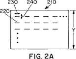
図2AおよびBを参照しつつ、本発明の第1の実施例を説明する。図2Aはスリットのパターン220を組み込んだマスク210を説明する。マスク210は、望ましくは水晶基板から作製し、図2Aに示したもののような、マスクパターンを形成する従来の技術によってエッチされた誘電体被膜或いは金属を含む。エッチスリット220は、スリット220に対応する特定の位置におけるサンプル170上に作製されるであろう装置に必要な寸法に合うように選択された横幅230である。例えば、スリット220は、横に約25マイクロメータでありこれによって25マイクロメータの半導体デバイスを作製する、或いは、複数部品の装置の場合は、装置内の経路(channel)をサンプル170に作製する。スリット220の縦の幅240は、サンプル170の核形成を回避するのに十分小さくし、かつ、各エキシマーパルスのラテラル結晶成長を最大化するため十分大きくするために、望ましくは約2から5マイクロメータの間とする。図2Aは通常のスリットのパターン220を説明するものであるが、膜170上に作製されるべき所望の微細構造に適合するようにどんなスリットのパターンも利用し得る。
【0020】
本発明においては、サンプル170の結晶領域を成長させるために、マスキングシステム150或いはサンプル移動ステージ180を動かすことによって、サンプル170をレーザパルス164に対して移動させる。サンプル170をY方向に移動し、マスク210をマスキングシステム150で使用した場合は、図2Bに示すように、結晶化された領域260を持つ処理されたサンプル250が形成される。それぞれの結晶化領域の横の幅270は、マスク210の横幅230とほぼ同じになる。各領域の縦の長さ280は、マスキングシステム150或いは移動ステージ180の移動によってもたらされるY方向の距離とほぼ同じになり、この縦の長さは、最終的な装置の特性に応じて選択すべきである。各結晶領域260は、長さと方位を制御された粒子のポリシリコンから成る。
【0021】
次に図3AおよびBを参照しつつ、本発明の第2の実施例を説明する。図3Aは、山がたのパターン320を組み込んだマスク310を示す。パターン320のそれぞれの山がたの一方の側の横の幅は、サンプル170に形成されるべき最終的な単一の結晶領域のサイズを決定することとなる。サンプル170をY方向に移動し、かつ、マスキングシステム150にマスク310を使用する場合は、図3Bに示すように、結晶化された領域360を持つ処理されたサンプル350が作製される。各結晶領域360は、ダイヤモンド状に整形された単結晶領域370と、各山の後側における、2つの長さの粒子であり方位を制御された多結晶シリコン領域380とから構成される。
【0022】
図2、3を参照しつつ説明した実施例は、シリコンサンプル170上に空間的に離れた装置を形成するのに好適であるが、シリコンサンプル170の少なくとも幾つかは最終的な半導体では利用されない。サンプル170上に作られ得る装置をより柔軟な構成で利用するために、以下の好適な実施例を説明することとする。
【0023】
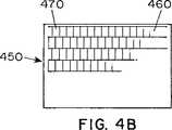
図4A、4Bを参照しつつ、本発明の第3の実施例を説明する。図4Aは、スリットパターン420を組み込んだマスク410を示す。各スリット420は、マスク全体にわたって延長されるべきものであり、従って、マスク上に均一化されたレーザビーム149の入射が可能になり、また、各スリットは、サンプル170の照射された領域において起こる何らかの核形成を防止するのに十分細くした縦の幅440を持たなければならない。縦の幅440は、入射レーザパルスのエネルギー密度、入射レーザパルスの持続時間、シリコン薄膜サンプルの厚さ、シリコン基板の温度および伝導性、を含む幾つかのファクターに依存する。例えば、室温で30nsであり、サンプルの完全溶融する閾値をわずかに超えるエネルギー密度を持つレーザパルスを500オングストロームの膜に照射する場合、スリットの縦幅は2マイクロメータを超えるものとすべきである。
【0024】
サンプル170をY方向に移動し、マスク410をマスキングシステム150に使用する場合は、図4Bに示すように、結晶化された領域460を持つ処理後のサンプル450が生成される。各結晶領域460は、粒子の長い、方位が制御された結晶470から構成される。サンプル410のマスキングスリット420の周期性421に依存して、粒子470の長さは、大きくなったり小さくなったりする。非晶質シリコン領域がサンプル領域170に残ることを防止するたにめには、Y方向への移動を少なくともマスク間の距離421と同じ長さにしなければならず、さらに当該距離を距離421よりも少なくとも1ミクロン大きくすることが好適であり、その結果、方位を制御された多結晶シリコン構造の初期段階において必然的に形成する小さな結晶が除去される。
【0025】
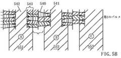
線のパターンを持つマスクを使用する特に好適な技法を説明する。図4Aに示すように4マイクロメータの縦の幅440を持つぎっしり詰まっており、各線が2マイクロメータの間隔で離間されているマスク線420のようなマスクを使用して、サンプル170は1つのレーザパルスで照射される。図5Aに示すように、レーザパルスは、サンプルの領域510,511,512を溶融し、ここで各溶融した領域は約4マイクロメータの幅520であり、約2マイクロメータの離間距離521で離れている。この第1のレーザパルスは、溶融境界530から始まり、溶融領域に成る照射された領域510,511,512において結晶成長の形成を生じさせ、それ故に、図5Bに示すように多結晶シリコン540を照射された領域に形成する。
【0026】
溶融境界530に形成される多数の小さな初期結晶541を除去するために、サンプル170は、Y方向に3マイクロメータ移動され、そして、再度ひとつのエキシマーレーザパルスが照射される。この第2の照射領域551,552,553は、残りの非晶質シリコン542と多結晶シリコン540の初期結晶領域543とを融解させるが、一方、多結晶シリコンの中央区画545を残したままにする。図5Cに示すように、中央区画545に形成される結晶構造は、溶融した領域542の固化に基づき外側に成長し、その結果、方位が制御され、粒子の長い多結晶シリコンデバイスがサンプル170上に形成される。
【0027】
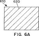
図6A、6Bを参照しつつ、本発明の第4の実施例を説明する。図6Aは、斜め線のパターン620を組み込んだマスク610を示す。サンプル170がY方向に移動され、マスク610をマスキングシステム150に使用する場合は、図6Bに示すように、結晶領域660を持つ処理されたサンプル650が生成される。各結晶領域660は、粒子を長くされ、方位が制御された結晶670から構成されることとなる。
【0028】
図4A、4Bと同じように上述した実施例では、移動方向は所望する結晶長さの依存する。また、4マイクロメータの幅の線620を持ち、それぞれが2マイクロメータで離間される図6Aに示したマスクを使用して、図5A〜Cを参照して説明した方法を容易に用いることが可能である。この実施例は、多結晶構造が前記軸に対して斜めになっていないため、XY軸に関して結晶の方位を向けられたディスプレイやその他のデバイスの製造の場合には、特に有利であり、従って、これらの装置の性能は、X或いはY座標に依存するものである。
【0029】
図7A、7Bを参照しつつ、本発明の第5の実施例を説明する。図7Aは、ずれた(offset)鋸歯状パターン720,721を組み込んだマスク710を示す。サンプル170がY方向に移動され、マスク710をマスキングシステム150に使用する場合は、図7Bに示すように、結晶化された領域760を持つ処理されたサンプル750が生成される。各結晶領域760は、斜め−方形の結晶770の配列から構成される。移動距離を鋸歯パターンの周期よりも僅かに大きくした場合は、結晶は6角形になる。本実施例は、大きなシリコン粒子の生成に有利であり、装置の性能を向上させ得るものである。
【0030】
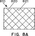
次は、図8A、8Bを参照しつつ、本発明の第6の実施例を説明する。図8Aは、斜めの交差したパターン821,822を組み込んだマスク810を示す。サンプル170がY方向に移動され、マスク810をマスキングシステム150に使用する場合は、図8Bに示すように、結晶化された領域860を持つ処理されたサンプル850が生成される。各結晶領域860は、ダイヤモンド状に整形された結晶870の配列から構成される。移動方向がパターンの周期よりもわずかに大きい場合は、結晶は正方形になる。この実施例も、大きなシリコン粒子の生成に有利であり、装置の性能を向上させ得るものである。
【0031】
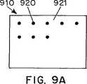
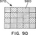
次に図9A〜Dを参照しつつ、本発明の第7の実施例を説明する。図9Aは、水玉パターン920を組み込んだマスク910を示す。この水玉マスク910は、逆転マスクであり、ここで水玉920に相当する部分がマスクされる領域であり、マスクの残部921が透過するところである。大きなシリコン結晶を製造するためには、この水玉パターンが、サンプル170上の結晶が所望されるところの点に関して連続的に移動され得る。例えば、図9Bに示すように、この水玉マスクは、第1のレーザパルスの後でYの正方向931に短い距離移動させ、第2のレーザパルスの後でXの正方向932に短い距離移動させ、第3のレーザパルスの後でYの負方向933に短い距離移動させ、大きな結晶の形成を促進させることができる。水玉の玉の離間距離がラテラル成長距離の2倍を越える距離である場合は、図9Cに示すように、結晶960が小さな粒子の多結晶シリコン領域961で離間された結晶960の結晶構造950が生成される。核形成を回避するためにこの離間距離がラテラル成長距離の2倍未満、或いは同じ距離である場合は、結晶980を持つ結晶構造970が、図9Dに示すように生成される。
【0032】
次に図10を参照しつつ、図9に関して実施される結晶成長プロセスを制御するために、コンピュータ100により実行されるステップを説明する。図10は、図1の本システムで実現される基本的なステップを説明するフローチャートである。図1に示した様々な電気機器は、プロセスを初期化するためにコンピュータによって1000で初期化される。それから、シリコン薄膜サンプルは、サンプル移動ステージ1005に装着即ちロードされる。このような装着は、コンピュータ100の制御下、手動でも、或いは機械的にも実現され得る。次に、サンプル移動ステージは、初期ポジション1015に移動され、この移動は、サンプル上の参照部位に位置合わせされることも含む得る。必要であれば、本システムの様々な光学要素が1020で焦点を合わせられる。その後、レーザは、所望のエネルギー密度と繰り返しレートになるように1025で安定化され、必要に応じて実行されるべき特定の処理に応じてシリコンサンプルを完全に溶融させる。必要であれば、レーザパルスの減衰が1030で精密に調整される。
【0033】
次に、1035でシャッターが開かれ、サンプルを1つのパルスの照射に曝し、これに応じて、連続ラテラル固化プロセスが開始する。1040で、サンプルは、X或いはY方向にスーパーラテラル成長距離未満の量だけ移動される。1045で、シャッターは再度開放され、サンプルを1つのパルスの照射に曝し、1050で、サンプルは再度X或いはY方向にスーパーラテラル成長距離未満の量だけ移動される。もちろん、ステップ1040でサンプルがX方向に移動された場合は、水玉を作成するためにステップ1050ではサンプルをY方向に移動するべきである。その後、1055でサンプルは第3のレーザパルスを照射される。サンプル移動と照射のプロセス1050,1055は、1060で繰り返すことができ、これにより4或いはそれよりも多くのレーザパルスで水玉領域を成長させることができる。
【0034】
次に、サンプル上のその他の領域が結晶化するために指定されていた場合は、サンプルは1065、1066で位置変えをされ、この結晶化プロセスは新たな領域上で繰り返される。結晶化のためにさらなる領域が指定されていない場合は、1070でレーザは閉じられ、1075でハードウェアは停止され、1080で本プロセスは終了する。もちろん、追加のサンプルの処理を所望する場合、或いは、本発明がバッチ処理用に利用される場合は、ステップ1005、1010、1035〜1065は各サンプルに対して繰り返され得る。
【0035】
前述した事項は、単に本発明の原理を説明したものである。前述した実施例に対しては、本明細書の教示において当業者が様々な修正や変形を行うことが自明である。例えば、シリコン薄膜170は、予めパターン化されたシリコン膜の島を持つサンプルによって置き換えることもできる。また、線のパターンマスクを使用して、図5A〜Cを参照しつつ説明したように2つのレーザパルスを使用して多結晶シリコンを成長させ、その後、90度回転させ、同じ方法を用いて四角形に整形された単一の結晶シリコンのアレイを生成することができる。従って、当業者は、本明細書で明示的に示されていない様々な方法やシステムを考え出し、本発明の本質の範囲内において本発明の原理を実現することができることを認識するべきである。
【図面の簡単な説明】
【図1】 本発明の好適な方法を実現するのに適したラテラル固化プロセスを実施するためのシステムの機能図である。
【図2A】 破線のパターンを持つマスクを示す説明図であ
【図2B】 図1のシステムで図2Aに示したマスクを使用することで得られた結晶化シリコン膜の説明図である。
【図3A】 山がたのパターンを持つマスクを示す説明図である。
【図3B】 図1のシステムで図3Aに示したマスクを使用することで得られた結晶化シリコン膜の説明図である。
【図4A】 線のパターンを持つマスクを示す説明図である。
【図4B】 図1のシステムで図4Aに示したマスクを使用することで得られた結晶化シリコン膜の説明図である。
【図5A】 線のパターンを使用して照射したシリコンサンプルの領域を示す説明図である。
【図5B】 最初の照射を行いかつサンプルを移動させた後ののパターンを使用して照射したシリコンサンプルの領域を示す説明図である。
【図5C】 第2の照射をした後の結晶化したシリコン膜を示す説明図である。
【図6A】 斜め線のパターンを持つマスクを示す説明図である。
【図6B】 図1のシステムで図6Aに示したマスクを使用することで得られた結晶化シリコン膜の説明図である。
【図7A】 鋸歯状のパターンを持つマスクを示す説明図である。
【図7B】 図1のシステムで図7Aに示したマスクを使用することで得られた結晶化シリコン膜の説明図である。
【図8A】 交差する斜め線のパターンを持つマスクを示す説明図である。
【図8B】 図1のシステムで図8Aに示したマスクを使用することで得られた結晶化シリコン膜の説明図である。
【図9A】 水玉のパターンを持つマスクを示す説明図である。
【図9B】 図9Aのマスクを使用してマスク移動を説明する指示図である。
【図9C】 図9Bに示したマスク移動スキームを使用して図1のシステムで図9Aに示したマスクを使用することで得られた結晶化シリコン膜の説明図である。
【図9D】 図9Bに示したマスク移動スキームを使用して図1のシステムで図9Aに示したマスクを使用することで得られた別の結晶化シリコン膜の説明図である。
【図10】 図1の本システムで実現されるステップを説明するフローチャートである。[0001]
BACKGROUND OF THE INVENTION
The present invention relates to a semiconductor processing method, and more particularly to a semiconductor processing method that can be performed at a low temperature.
[0002]
Explanation of related fields
In the field of semiconductor processing, several attempts have been made to convert amorphous silicon thin films into polycrystalline films using lasers. For example, "Crystalline Si Film for Integrated Active-Matrix Liquid-Crystal Displays (11MRS Bullitin 39 (1996))" by James Im et al. Provides an overview of conventional excimer laser annealing techniques. In such systems, the excimer laser beam is shaped into a long beam, typically up to 30 cm long and 500 micrometers wide or more. This shaped beam is scanned over a sample of amorphous silicon, which is melted and converted to polycrystalline silicon by resolidification of the sample.
[0003]
The use of conventional excimer laser annealing techniques to produce polycrystalline silicon is problematic for several reasons. First, the polycrystalline silicon produced by this method is typically small particles, random microstructures, and non-uniform particle sizes, resulting in poor and non-uniform equipment. Yes, so the yield is low. Second, in order to obtain an acceptable level of performance, the production capacity for the production of polycrystalline silicon must be reduced. The method also generally requires a controlled atmosphere and preheating of the amorphous silicon sample, which leads to a reduction in throughput rate. Accordingly, there is a need in the art to produce higher quality polycrystalline silicon at a greater throughput rate. Similarly, there is a need for a manufacturing technique that forms larger, more uniform microstructured polycrystalline silicon thin films to be used in the manufacture of higher quality devices such as flat panel displays.
[0004]
Summary of the Invention
An object of the present invention is to provide a technique for forming a polycrystalline thin film semiconductor with uniform, large particles and controlled grain boundary positions using a sequential lateral solidification process. is there.
It is a further object of the present invention to form polycrystalline silicon that is large in size and engineered grain boundary locations throughout substantially the entire semiconductor sample.
Yet another object of the present invention is to provide a technique for the manufacture of semiconductor devices that is convenient for manufacturing displays and other products, in which the majority of semiconductor grain boundaries are oriented in the device. Can be controllably aligned or displaced relative to the current flow direction of
[0005]
To achieve these and other objectives that will also become apparent in the description of the following part of the specification, the present invention addresses the disclosed polycrystalline silicon thin film processing. It is to provide a method for converting to a thin film. In a preferred embodiment, the method includes generating a series of excimer laser pulses and modulating each excimer laser pulse in the series of excimer laser pulses in a controllable state to a predetermined fluence (energy density). And uniformizing each of the modulated laser pulses in the series in a predetermined plane, and controlling the homogenized fluence in the series with a two-dimensional pattern of slits. Masking a portion of each of the laser pulses generated to produce a controlled series of linearly patterned beamlet fluence pulses (each slit in the two-dimensional pattern is in this slit). In the region of the silicon thin film sample irradiated by the corresponding beamlet. Thin and narrow enough to prevent the induction of nucleation), the amorphous silicon thin film sample is irradiated with a series of beamlets patterned with fluence controlled slits to form the pattern Melting a portion corresponding to each of the beamlets patterned with a controlled fluence in the series of beamlet pulses, and controlling the pulse of the fluence of the beamlets patterned with the slits. Moving the relative position of the sample relative to each other in a controllable manner, whereby the amorphous silicon thin film is processed and converted into a single or polycrystalline silicon thin film.
[0006]
In a preferred embodiment, the step of generating the masking pulse comprises extending substantially linearly parallel to one direction of the uniformized plane and substantially parallel and straight spaced apart by a predetermined separation distance. A series of pulses with controlled fluence of beamlets patterned with slits by masking a portion of each of the uniformed fluence controlled laser pulses in the two-dimensional pattern of slits. Is generated. Given the movement, the relative position of the sample is continuously controllable, and the fluence of the slit patterned beamlet is substantially perpendicular to each of the controlled pulses, with a predetermined slit spacing. Suitable to move over distance, thereby processing the amorphous thin film sample to convert it into a polycrystalline silicon thin film with long grains, ie, long grained and oriented crystals It is.
[0007]
In a particularly preferred embodiment, the step of masking and generating the pulses comprises transferring a portion of each of the controlled and uniform fluence laser pulses in the series to a predetermined spacing less than the predetermined width. Masked with a two-dimensional pattern of substantially parallel and straight slits of a predetermined width, which is parallel to one direction of the uniformed plane and extended linearly, and patterned with slits. Generating a series of pulses of controlled fluence of the normalized beamlet. In this configuration, the moving step moves the relative position of the sample by a distance less than the predetermined width in the direction perpendicular to each of the controlled pulse fluences of the beamlets patterned by the slit. Thus, an amorphous silicon thin film sample is processed and converted into a polycrystalline silicon thin film having long grains and crystals with controlled orientation by using only two laser pulses. In one example, the predetermined width is about 4 micrometers, the predetermined separation distance is about 2 micrometers, and the travel distance is about 3 micrometers.
[0008]
In another preferred embodiment, the step of masking and generating the pulses comprises transferring a portion of each of the controlled and uniform fluence laser pulses in the series to one of the uniform planes. Of a beamlet patterned with a slit, masked with a slit of a substantially parallel and straight two-dimensional pattern extended linearly at an angle of substantially 45 degrees to the direction and spaced at a predetermined separation distance. Generating a series of pulses of controlled fluence. In this configuration, the moving step is performed over a predetermined slit separation distance in a direction parallel to one direction of the uniformized plane in a state in which the relative position of the sample can be continuously controlled ( over), thereby processing the amorphous thin film sample to convert it into a polycrystalline silicon thin film with long particles and controlled orientation and with crystals displaced in the direction of the XY axis of the silicon thin film .
[0009]
In yet another preferred embodiment, the step of generating the masking pulses comprises the step of intersecting straight slits (first first) of each of the controlled and uniform fluence laser pulses in the series. The slit groups are separated by a first predetermined separation distance and are linearly extended at an angle of substantially 45 degrees with respect to the first direction of the uniformed plane. Are linearly extended at an angle of substantially 45 degrees with respect to the second direction of the homogenized plane, separated by a second predetermined spacing distance, and Masking with a two-dimensional pattern of substantially 90 degrees) to produce a series of pulses of controlled fluence of beamlets patterned with slits. A corresponding moving step moves the relative position of the sample over the first predetermined slit spacing in a direction parallel to the first direction of the homogenized plane, The silicon thin film is processed to be converted into a polycrystalline silicon thin film having crystals shaped into a large diamond shape.
[0010]
In yet another embodiment, the step of generating the masking pulses comprises the step of separating a portion of each of the controlled and uniform fluence laser pulses in the series with a predetermined spacing interval. Masked with a two-dimensional pattern of sawtooth shaped slits extending generally parallel to one direction, thereby processing the amorphous thin film sample and forming a beamlet patterned with slits. Generate a series of pulses of controlled fluence. In this configuration, the moving step is sequential in a state where the relative position of the sample is controllable, and the fluence of beamlets patterned with slits is perpendicular to each of the controlled pulses, Substantially moved over the predetermined slit separation distance, extended linearly at an angle of substantially 45 degrees with respect to one direction of the uniformed plane, and substantially spaced at a predetermined separation distance Is masked with a two-dimensional pattern of slits parallel and straight to produce a series of pulses in which the fluence of beamlets patterned at the slit is controlled. In this configuration, the moving step is continuously performed in a state in which the relative position of the sample is controllable in a direction parallel to one direction of the uniformized plane, substantially over the predetermined slit separation interval. Thus, the amorphous silicon thin film sample is processed, and the orientation is controlled so that the direction is shifted with respect to the XY axis of the silicon thin film, and the thin film is converted into a polycrystalline silicon thin film having long crystals of particles.
[0011]
In yet another preferred embodiment, the step of generating the masking pulse comprises the step of generating a two-dimensional pattern of straight slits intersecting a portion of each of the controlled and uniform fluences in the series. The first slit group is separated by a first predetermined separation distance and is extended linearly at an angle of substantially 45 degrees with respect to the first direction of the uniform plane, and the second slit group Are linearly extended at an angle of substantially 45 degrees with respect to the second direction of the uniformized plane and spaced apart by a second predetermined spacing distance, and substantially linear with the first slit group. At a 90 degree angle) and generating a controlled series of pulses to control the fluence of beamlets patterned with slits. The corresponding moving step is sequential, i.e. continuous, in such a way that the relative position of the sample is controllable substantially parallel to the first direction of the homogenized plane and substantially over the first predetermined separation distance. Thus, the amorphous silicon thin film sample is processed and converted into a polycrystalline silicon thin film having crystals shaped into a large diamond shape.
[0012]
In yet another embodiment,
The step of masking and generating a pulse is configured such that a portion of each of the controlled and uniformed fluences in the series is separated by a predetermined separation distance and generally in one direction of the uniformized plane. Masking with a two-dimensional pattern of sawtooth shaped slits extending parallel to the edges, thereby producing a controlled series of pulses for the fluence of the beamlets patterned with the slits. In this configuration, the moving step moves the relative position of the sample substantially over the predetermined slit separation distance in a direction perpendicular to each of the fluence-controlled pulses of the beam patterned with the slit. The film is continuously moved in a controllable state, whereby the amorphous silicon thin film is processed and converted into a polycrystalline silicon thin film having large hexagonal crystals.
[0013]
In a modified embodiment, an alternative technique is provided that uses a polka dot pattern to process an amorphous silicon film and convert it to a polycrystalline silicon film. The technique includes generating a series of excimer laser pulses, homogenizing each of the series of laser pulses in a predetermined plane, and substantially substituting a portion of each of the series of homogenized laser pulses. Generating a series of pulses of beamlets patterned with polka dots masked with an opaque two-dimensional pattern, and irradiating the amorphous silicon thin film with the beamlets patterned with the series of polka dots, Melting a portion corresponding to each of the beamlet pulses patterned with the series of polka dots, at a distance less than a super lateral grown distance of the sample, and to two vertical axes By alternating the direction, the phase of the sample for each pulse of beamlets patterned with polka dots Continuously moving the pair position in a controllable manner, whereby the amorphous silicon thin film sample is processed and converted to a polycrystalline silicon thin film.
[0014]
The accompanying drawings are included in and constitute a part of this disclosure, and serve to explain the preferred embodiments of the invention and to explain the principles of the invention.
DESCRIPTION OF PREFERRED EMBODIMENTS
The present invention provides a technique for producing a uniform, long grain, controlled grain boundary position polycrystalline silicon thin film semiconductor using a continuous lateral solidification process. In order to fully understand these techniques, the continuous lateral solidification process must be described.
[0015]
The continuous lateral solidification process is a technique that forms a long particle silicon structure through a small amount of movement of a silicon sample in a single direction during successive pulses emitted from an excimer laser. As each pulse is absorbed by the sample, a small area of the sample is completely melted and then laterally solidified and converted into a crystalline area generated by the preceding pulse in the set of pulses. The
[0016]
A particularly suitable continuous lateral solidification process and apparatus for performing the process are described in the title “Systems and Methods Using Continuous Lateral Solidification to Generate Single Crystal or Polycrystalline Silicon Thin Films at Low Temperatures (filed with this application). , Is inherited by the same applicant as this application) and is incorporated herein by reference. Although the foregoing disclosure has been made with reference to the specific techniques disclosed in the above-mentioned co-pending applications, other continuous lateral solidification techniques are readily applicable to the present invention. Should be understood.
[0017]
Although described in FIG. 1 as a preferred embodiment in our co-pending patent application, the system includes an
[0018]
As described in more detail in our co-pending application, generating a plurality of excimer laser pulses of a given fluence, modulating the fluence of the excimer laser pulses in a controllable manner, Homogenizing the modulated laser pulse in a predetermined plane, masking a portion of the modulated and uniform laser pulse to convert it into a patterned beamlet, and amorphous Irradiating the silicon thin film sample with the patterned beamlet and consequently melting the portion corresponding to the irradiated portion of the beamlet; and the sample with respect to the patterned beamlet; And controllably moving with respect to the controlled modulation, whereby said The amorphous silicon by continuously moving the sample relative to the turned beamlet and irradiating a fluence patterned beamlet that changes to a corresponding sequential (continuous) position. The thin film sample is processed and converted to a single crystal or polycrystalline silicon thin film. The following embodiments of the invention will be described with reference to the processing techniques described above.
[0019]
A first embodiment of the present invention will be described with reference to FIGS. 2A and 2B. FIG. 2A illustrates a
[0020]
In the present invention, the
[0021]
Next, a second embodiment of the present invention will be described with reference to FIGS. 3A and 3B. FIG. 3A shows a
[0022]
The embodiments described with reference to FIGS. 2 and 3 are suitable for forming spatially separated devices on the
[0023]
A third embodiment of the present invention will be described with reference to FIGS. 4A and 4B. FIG. 4A shows a
[0024]
If the
[0025]
A particularly preferred technique using a mask with a line pattern is described. Using a mask such as
[0026]
In order to remove a number of small initial crystals 541 formed at the melt boundary 530, the
[0027]
A fourth embodiment of the present invention will be described with reference to FIGS. 6A and 6B. FIG. 6A shows a
[0028]
In the embodiment described above as in FIGS. 4A and 4B, the direction of movement depends on the desired crystal length. It is also possible to easily use the method described with reference to FIGS. 5A-C using the mask shown in FIG.
[0029]
A fifth embodiment of the present invention will be described with reference to FIGS. 7A and 7B. FIG. 7A shows a
[0030]
Next, a sixth embodiment of the present invention will be described with reference to FIGS. 8A and 8B. FIG. 8A shows a
[0031]
Next, a seventh embodiment of the present invention will be described with reference to FIGS. FIG. 9A shows a
[0032]
Referring now to FIG. 10, the steps performed by
[0033]
Next, at 1035, the shutter is opened, exposing the sample to one pulse of irradiation, and in response, the continuous lateral solidification process begins. At 1040, the sample is moved in the X or Y direction by an amount less than the super lateral growth distance. At 1045, the shutter is opened again, exposing the sample to one pulse of irradiation, and at 1050, the sample is again moved in the X or Y direction by an amount less than the super lateral growth distance. Of course, if the sample is moved in the X direction at step 1040, the sample should be moved in the Y direction at
[0034]
Next, if other regions on the sample have been designated to crystallize, the sample is repositioned at 1065, 1066 and the crystallization process is repeated on the new region. If no additional regions are designated for crystallization, the laser is closed at 1070, the hardware is stopped at 1075, and the process ends at 1080. Of course, if processing of additional samples is desired, or if the present invention is utilized for batch processing,
[0035]
The foregoing is merely illustrative of the principles of the invention. It will be apparent to those skilled in the art that various modifications and variations can be made to the embodiments described above by following the teachings herein. For example, the silicon
[Brief description of the drawings]
FIG. 1 is a functional diagram of a system for performing a lateral solidification process suitable for implementing the preferred method of the present invention.
FIG. 2A is an explanatory diagram showing a mask having a broken line pattern.
2B is an explanatory diagram of a crystallized silicon film obtained by using the mask shown in FIG. 2A in the system of FIG.
FIG. 3A is an explanatory diagram showing a mask having a crest pattern.
3B is an explanatory diagram of a crystallized silicon film obtained by using the mask shown in FIG. 3A in the system of FIG.
FIG. 4A is an explanatory diagram showing a mask having a line pattern;
4B is an explanatory diagram of a crystallized silicon film obtained by using the mask shown in FIG. 4A in the system of FIG.
FIG. 5A is an illustration showing a region of a silicon sample irradiated using a line pattern.
FIG. 5B is an explanatory diagram showing a region of a silicon sample irradiated using the pattern after the first irradiation and the sample are moved.
FIG. 5C is an explanatory view showing a crystallized silicon film after the second irradiation.
FIG. 6A is an explanatory diagram showing a mask having an oblique line pattern;
6B is an explanatory diagram of a crystallized silicon film obtained by using the mask shown in FIG. 6A in the system of FIG.
FIG. 7A is an explanatory diagram showing a mask having a sawtooth pattern.
7B is an explanatory diagram of a crystallized silicon film obtained by using the mask shown in FIG. 7A in the system of FIG.
FIG. 8A is an explanatory diagram showing a mask having a pattern of intersecting diagonal lines.
8B is an explanatory diagram of a crystallized silicon film obtained by using the mask shown in FIG. 8A in the system of FIG.
FIG. 9A is an explanatory diagram showing a mask having a polka dot pattern.
FIG. 9B is an instruction diagram illustrating mask movement using the mask of FIG. 9A.
9C is an illustration of a crystallized silicon film obtained using the mask shown in FIG. 9A in the system of FIG. 1 using the mask movement scheme shown in FIG. 9B.
9D is an illustration of another crystallized silicon film obtained by using the mask shown in FIG. 9A in the system of FIG. 1 using the mask movement scheme shown in FIG. 9B.
FIG. 10 is a flowchart for explaining steps realized in the system of FIG. 1;
Claims (21)
Translated fromJapanese(a)それぞれがほぼ所定のサイズを持つ、一連のエキシマーレーザパルスを生成するステップと、
(b)所定の幅の1つまたは複数のスリットを持つマスクで、前記一連のエキシマーレーザパルスをマスクして、各ビームレットが前記所定のレーザパルスのサイズに対応する長さと、前記所定のスリットの幅とで規定される形状を持つような、前記レーザパルスに対応する1つまたは複数の第1のレーザビームレットを生成するステップと、
(c)シリコン薄膜に、前記1つまたは複数の第1のレーザビームレットを照射し、前記1つまたは複数のレーザビームレットに対応した、前記シリコン薄膜の第1の領域を溶融させるステップと、
(d)第2のレーザパルスに対応する1つまたは複数のレーザビームレットが前記シリコン薄膜の第2の位置に入射するように、前記シリコン薄膜および前記エキシマーレーザパルスの少なくとも1つを、もう1つのものに対して相対的に移動するステップと、
(e)ステップ(d)の後、前記シリコン薄膜の第2の領域を、前記第2のパルスに対応する前記1つまたは複数のレーザビームレットで照射して、前記第2の薄膜位置にある前記第2の領域を溶融させるステップであって、前記第2の領域が前記第1の領域に部分的に重なる、ステップと、を含み、
前記照射された領域の各々は、前記薄膜の厚さ方向に溶融され、ラテラル成長が、前記薄膜の各溶融領域でなされ、前記レーザビームレットの幅は、該レーザビームレットにより照射された前記薄膜の領域において核形成の誘発を防止するために十分狭くすることを特徴とする方法。In a method of processing an amorphous silicon thin film to convert it to a polycrystalline silicon thin film,
(A) generating a series of excimer laser pulses, each having a substantially predetermined size;
(B) masking the series of excimer laser pulses with a mask having one or more slits of a predetermined width, each beamlet having a length corresponding to the size of the predetermined laser pulse, and the predetermined slit Generating one or more first laser beamlets corresponding to the laser pulse having a shape defined by:
(C) irradiating the silicon thin film with the one or more first laser beamlets to melt a first region of the silicon thin film corresponding to the one or more laser beamlets;
(D) at least one of the silicon thin film and the excimer laser pulse is another one such that one or more laser beamlets corresponding to the second laser pulse are incident on the second position of the silicon thin film; Moving relative to one thing,
(E) After step (d), the second region of the silicon thin film is irradiated with the one or more laser beamlets corresponding to the second pulse and is at the second thin film position. a step of melting the second region, the second region partially overlaps the firstregion, comprises the steps, a,
Each of the irradiated regions is melted in the thickness direction of the thin film, lateral growth is performed in each molten region of the thin film, and the width of the laser beamlet is the thin film irradiated by the laser beamlet. A methodcharacterized by narrowing sufficiently to prevent induction of nucleation in the region of
前記第2の領域は、前記第1の領域の半分未満でそこに重なる、
ことを特徴とする方法。The method of claim 1, wherein
The second region overlaps with less than half of the first region;
A method characterized by that.
前記薄膜および前記エキシマーレーザパルスの少なくとも1つが、
もう1つのもの対して相対的に、3マイクロメータの距離で移動される、
ことを特徴とする方法。The method of claim1 , wherein
At least one of the thin film and the excimer laser pulse is
Moved relative to the other by a distance of3 micrometers,
A method characterized by that.
前記薄膜および前記エキシマーレーザパルスの少なくとも1つが、
前記ラテラル成長を超え、前記ビームレットの幅未満の距離で移動される、
ことを特徴とする方法。The method of claim 1, wherein
At least one of the thin film and the excimer laser pulse is
Moved beyond the lateral growth and less than the width of the beamlet,
A method characterized by that.
前記スリットが、
前記マスク上に前記レーザパルス照射が可能である限りは前記マスクの全体にわたって延在する、
ことを特徴とする方法。The method of claim 1, wherein
The slit is
As long as the laser pulse irradiation is possible on the mask, it extends throughout the mask,
A method characterized by that.
(a)所定のフルエンス(fluence)のエキシマーレーザパルスを複数生成するエキシマーレーザと、
(b)前記エキシマーレーザによって出射された前記エキシマーレーザパルスの前記フルエンスを制御可能に変調する、光学的に前記エキシマーレーザに結合されている、エネルギー密度変調器と、
(c)所定の平面において前記変調されたレーザパルスを均一化し、これら均一化されたレーザパルスの各々がほぼ所定のサイズを持つような、前記エネルギー密度変調器と光学的に結合されている、ビーム均一化器と、
(d)前記均一化され変調されたレーザパルスの各々をマスクして、各均一化されたレーザパルスに対応する1つまたは複数のビームレットを生成し、各ビームレットは、前記スリットの幅に対応する、前記所定のレーザパルスのサイズおよび幅に対応する長さによって規定される形状を持つために、前記ビーム均一化器に光学的に結合されているとともに移動に適合した、所定の幅を有する1つまたは複数のスリットを有するマスクと、
(e)各レーザパルスのための前記1つまたは複数のレーザビームレットを受けて、前記レーザビームレットの形状に対応して、そこに置かれた何らかのシリコン薄膜の一部を溶融させるための、移動に適合され、前記マスクに光学的に結合されている、サンプルステージと、
(f)前記マスクおよび前記サンプルステージの相対的位置および前記エキシマーレーザパルスの前記制御可能なフルエンス変調を制御し、前記マスクおよび前記サンプルステージの前記相対的位置にあわせて、前記フルエンス変調および前記エキシマーパルス生成を調整して、これによって、その連続的な場所に対応する場所における各レーザパルスのための1つまたは複数のレーザビームレットによる前記薄膜の照射によって、および、前記マスクに対して相対的な前記サンプルステージの連続移動によって、前記シリコン薄膜を処理して多結晶シリコン薄膜に変換する、前記エネルギー密度変調器および前記エキシマーレーザに結合されている、コンピュータと、
を含むシステム。In a system that processes a silicon thin film and converts it to a polycrystalline silicon thin film,
(A) an excimer laser that generates a plurality of excimer laser pulses of a predetermined fluence;
(B) an energy density modulator optically coupled to the excimer laser that controllably modulates the fluence of the excimer laser pulse emitted by the excimer laser;
(C) homogenizing the modulated laser pulses in a predetermined plane and optically coupled with the energy density modulator such that each of the homogenized laser pulses has a substantially predetermined size; A beam homogenizer,
(D) masking each of the homogenized and modulated laser pulses to generate one or more beamlets corresponding to each homogenized laser pulse, each beamlet having a width of the slit; corresponding,for single lifting a shape defined by a length corresponding to the size and width of the predetermined laserpulse, adapted to move with and optically coupled to said beam homogenizing unit, a predetermined width A mask having one or more slits having :
(E) receiving the one or more laser beamlets for each laser pulse and melting a portion of any silicon thin film placed thereon corresponding to the shape of the laser beamlet; A sample stage adapted for movement and optically coupled to the mask;
(F) controlling the relative position of the mask and the sample stage and the controllable fluence modulation of the excimer laser pulse, and adjusting the fluence modulation and the excimer according to the relative position of the mask and the sample stage. Adjusting the pulse generation, thereby irradiating the thin film with one or more laser beamlets for each laser pulse at a location corresponding to its continuous location, and relative to the mask A computer coupled to the energy density modulator and the excimer laser to process and convert the silicon thin film into a polycrystalline silicon thin film by continuous movement of the sample stage;
Including system.
前記システムがコンピュータによって実行可能な命令:
(g)シリコン薄膜に前記レーザビームレットを照射して、前記マスクにおける前記所定のスリットパターンの形状に対応して、前記薄膜の第1の領域を溶融させるステップ、および、
(h)前記マスクの寸法に基づき、第2の位置に到達するように、前記エキシマーレーザパルスと前記薄膜の一方に対して相対的に、前記エキシマーレーザパルスと前記薄膜とのうちの少なくとも1つを移動させるステップ、
を含む、
ことを特徴とするシステム。The system of claim6 , wherein
Instructions that the system can execute by a computer:
(G) irradiating the silicon thin film with the laser beamlet to melt the first region of the thin film corresponding to the shape of the predetermined slit pattern in the mask; and
(H) at least one of the excimer laser pulse and the thin film relative to one of the excimer laser pulse and the thin film so as to reach a second position based on the dimension of the mask; Step to move the
including,
A system characterized by that.
(a)各々がほぼ所定のサイズを持つ、複数のエキシマーレーザパルスを生成するパルスエキシマーレーザと、
(b)前記レーザパルスの各々をマスクして、各レーザパルスに対応して1つまたは複数のレーザビームレットを生成し、このようにして、各ビームレットが、前記スリットの幅に対応した幅と前記所定のレーザパルスサイズに対応した長さとによって規定される形状を持たせるような、前記エキシマーレーザパルスに光学的に結合されているとともに移動に適合した、所定の幅を持つ1つまたは複数のスリットを持つマスクと、
(c)各レーザパルスのための前記1つまたは複数のレーザビームレットを受けて、前記レーザビームレットの形状に対応して、そこに置かれた何らかのシリコン薄膜の一部を溶融させる、光学的に前記マスクに結合され、移動するように適合されている、サンプルステージと、
(d)前記マスクと前記サンプルステージとの相対的位置および前記エキシマーレーザパルスを制御し、前記マスクと前記サンプルステージとの前記相多的位置にあわせて前記エキシマーレーザパルスを調整する、前記サンプルステージと前記エキシマーレーザとに結合されている、コンピュータと、
(e)その場所の対応する連続的な場所で各レーザパルスのための1つまたは複数のレーザビームレットによる、前記薄膜の照射および前記マスクに対する相対的な前記サンプルステージの連続的な移動によって、前記シリコン薄膜を処理することによって多結晶シリコン薄膜に変換する変換し、ここで、照射された各々が前記薄膜の厚さ方向に溶融し、ラテラル成長が前記薄膜の各溶融場所でなされるような、コンピュータ可読な媒体上の命令と、
を含むシステム。A system for processing a silicon thin film to convert it into a polycrystalline silicon thin film,
(A) a pulsed excimer laser that generates a plurality of excimer laser pulses, each having a substantially predetermined size;
(B) masking each of the laser pulses to generate one or more laser beamlets corresponding to each laser pulse, thus each beamlet having a width corresponding to the width of the slit One or more having a predetermined width optically coupled to the excimer laser pulseand adapted for movement so as to have a shape defined by a length corresponding to the predetermined laser pulse size A mask with slits,
(C) receiving the one or more laser beamlets for each laser pulse and melting a portion of any silicon thin film placed thereon corresponding to the shape of the laser beamlet; A sample stage coupled to the mask and adapted to move;
(D) controlling the relative position between the mask and the sample stage and the excimer laser pulse, and adjusting the excimer laser pulse in accordance with the multi-position between the mask and the sample stage; And a computer coupled to the excimer laser;
(E) by irradiation of the thin film and continuous movement of the sample stage relative to the mask by one or more laser beamlets for each laser pulse at a corresponding continuous location at that location; The silicon thin film is converted into a polycrystalline silicon thin film by processing, where each irradiated melts in the thickness direction of the thin film, and lateral growth occurs at each melting point of the thin film Instructions on a computer readable medium;
Including system.
前記システムがコンピュータによって実行可能な命令:
(g)シリコン薄膜に前記レーザビームレットを照射して、前記マスクにおける前記所定のスリットパターンの形状に対応して、前記薄膜の第1の領域を溶融させるステップ、および、
(h)前記マスクの寸法に基づき、第2の位置に到達するように、前記エキシマーレーザパルスと前記薄膜の一方に対して相対的に、前記エキシマーレーザパルスと前記薄膜とのうちの少なくとも1つを移動させるステップ、
を含む、
ことを特徴とするシステム。The system of claim8 , wherein
Instructions that the system can execute by a computer:
(G) irradiating the silicon thin film with the laser beamlet to melt the first region of the thin film corresponding to the shape of the predetermined slit pattern in the mask; and
(H) at least one of the excimer laser pulse and the thin film relative to one of the excimer laser pulse and the thin film so as to reach a second position based on the dimension of the mask; Step to move the
including,
A system characterized by that.
シリコン粒子の長さよりも大きく、かつ、前記シリコン粒子の長さの2倍よりも小さいような、ビーム幅を持つレーザビームの第1のショットを使って、前記インターフェイスまで前記シリコン膜の区画を完全に溶融させることによって、ある長さを持つシリコン粒子を成長させるステップと、
前記レーザビームの第2のショットを使って、前記成長したシリコン粒子の部分を再溶融させることによって、前記成長したシリコン粒子の前記長さを成長させるステップと、
を含み、
前記再溶融させた部分が、前記レーザビームの前記ビーム幅の二分の一を超える長さで、前記基板に対して相対的に前記レーザビームを離間させることによって決定される、
ような方法。A method of annealing a silicon film having an interface with the underlying surface,
Greater than the length of thesilicon particles, and the two times smaller as well than the length of the silicon particles, with the first shot of laser beam having a beam width, the complete section of the silicon layer to said interface Growing silicon particles having a certain length by melting into
Growing the length of the grown silicon particles by remelting a portion of the grown silicon particles using a second shot of the laser beam;
Including
The remelted portion is determined by separating the laser beam relative to the substrate by a length greater than one half of the beam width of the laser beam;
Like method.
前記シリコン膜が前記レーザビームでスキャンされる、
ことを特徴とする方法。The method of annealing a silicon film according to claim10 ,
The silicon film is scanned with the laser beam;
A method characterized by that.
前記シリコン粒子を成長させるステップ、前記シリコン膜に対して相対的に前記レーザビームを離間させるステップ、前記成長したシリコン粒子の一部を再溶融させるステップ、および、前記シリコン膜に対して相対的に前記レーザビームを再度離間させるステップが繰り返されることによって、前記シリコン膜がスキャンされる、
ことを特徴とする方法。The method of annealing a silicon film according to claim10 ,
Growing the silicon particles, separating the laser beam relative to the silicon film, remelting a portion of the grown silicon particles, and relative to the silicon film The silicon film is scanned by repeating the step of separating the laser beams again.
A method characterized by that.
前記レーザビームの第1のショットによって成長した前記シリコン粒子の長さが、2から4マイクロメートルである、
ことを特徴とする方法。The method of annealing a silicon film according to claim10 ,
The length of the silicon particles grown by the first shot of the laser beam is2 to 4 micrometers;
A method characterized by that.
前記レーザビームの第2のショットによって、前記シリコン粒子の長さが、4から8マイクロメートルに増加される、
ことを特徴とする方法。The method of annealing a silicon film according to claim13 ,
A second shot of the laser beam increases the length of the silicon particles from4 to 8 micrometers;
A method characterized by that.
前記シリコン膜が、前記レーザビームの第1のショットの前は非晶質シリコンである、
ことを特徴とする方法。The method of annealing a silicon film according to claim10 ,
The silicon film is amorphous silicon before the first shot of the laser beam;
A method characterized by that.
前記シリコン粒子が、大気圧で成長され、かつ、長くされる、
ことを特徴とする方法。The method of annealing a silicon film according to claim10 ,
The silicon particles are grown and lengthened at atmospheric pressure;
A method characterized by that.
前記レーザビームが、10マイクロメートル未満のビーム幅を持つ、
ことを特徴とする方法。The method of annealing a silicon film according to claim10 ,
The laser beam has a beam width of less than 10 micrometers;
A method characterized by that.
レーザビームによって照射される前記シリコン膜の区画における核生成を避けるために十分な狭さであるビーム幅を持つレーザビームのショットを使って、前記インターフェイスまで前記シリコン膜の前記区画を完全に溶融させることによって、ある長さを持つシリコン粒子を成長させるステップと、
前記レーザビームの第2のショットを使って前記成長させたシリコン粒子の一部を完全に再溶融させることによって前記成長させたシリコン粒子の前記長さを増加させるステップであって、前記レーザビームの前記ビーム幅の二分の一を超える長さの基板に対して相対的に前記レーザビームをずらすことによって、前記再溶融させる部分が決定されるようなステップと、
を含む方法。A method of annealing a silicon film that has an interface with the underlying surface,
Using shot of a laser beam having a beam width that is narrow enoughto nucleate order toavoid the section of the silicon film is irradiated by a laser beam, complete melting of the partition of the silicon layer to said interface Growing silicon particles having a certain length, and
Increasing the length of the grown silicon particles by completely remelting a portion of the grown silicon particles using a second shot of the laser beam, comprising: The portion to be remelted is determined by shifting the laser beam relative to a substrate having a length greater than one half of the beam width;
Including methods.
(a)一連のエキシマーレーザパルスを生成するステップと、
(b)マスクの開口の所定のパターンで、前記一連のレーザパルスの各々の一部をマスクするステップであって、前記レーザパルスで照射される前記シリコン膜の前記区画における核生成を避けるのに、前記開口が十分な狭さを持つようなステップと、
(c)前記レーザパルスの少なくとも1つを前記薄膜サンプルに照射して、前記マスクの開口の所定のパターンの形状に対応して前記薄膜サンプルの第1の領域を溶融せしめるステップと、
(d)第2の位置に到達するように、前記エキシマーレーザパルスと前記薄膜サンプルのうちの一方に対して相対的に、前記エキシマーレーザパルスと前記薄膜サンプルとのうちの少なくとも1つを移動させるステップと、
(e)ステップ(d)の後、前記ビームパルスの少なくとも1つを使って、前記薄膜サンプルの第2の領域を照射し、この領域は、前記第2の領域を溶融させるために、前記一連のパルスを使って前記第2の位置の区画に対応し、この第2の領域は、前記第1の領域の二分の一未満と重なるようなステップと、
を含む方法。A method of processing an amorphous silicon thin film sample to convert it to a polycrystalline silicon thin film,
(A) generating a series of excimer laser pulses;
(B) a predetermined pattern of openings in the mask, a step of masking a portion of each of said series of laser pulses, No Keruavoid nucleation in the compartment of the silicon film is irradiated with the laser pulses And a step in which the opening is sufficiently narrow;
The at least one of (c) the laser pulse is irradiated on the thin film sample, a first step of Ruallowed melting region of the thin film sample in response to the shape of a predetermined pattern of openings of said mask,
(D) moving at least one of the excimer laser pulse and the thin film sample relative to one of the excimer laser pulse and the thin film sample so as to reach a second position; Steps,
(E) After step (d), at least one of the beam pulses is used to irradiate a second region of the thin film sample, which region is used to melt the second region. The second region corresponds to a section of the second location using a pulse of the second region, and the second region overlaps less than one half of the first region;
Including methods.
シリコン粒子の長さよりも大きく、かつ、前記シリコン粒子の長さの2倍未満であるような、ビーム幅を持つレーザビームの第1のショットを使って、前記インターフェイスまで、前記シリコンの区画を完全に溶融させることによって、ある長さを持つシリコン粒子を成長させるステップと、
前記レーザビームの第2のショットを使って前記成長させたシリコン粒子の一部を完全に再溶融させることによって、前記成長させたシリコン粒子の長さを増加させるステップであって、2つのレーザショットを使って、粒子が長く方位的に制御された結晶を持つ多結晶シリコンに前記シリコン薄膜を変換するために選択されたような離間距離で、前記基板に対して相対的に前記レーザビームをずらすことによって、前記再溶融される領域が決定されるようなステップと、
を含む方法。A method of annealing a silicon film that has an interface with the underlying surface,
Using a first shot of a laser beam with a beam width that is greater than the length of the silicon particles and less than twice the length of the silicon particles, the silicon section is completely completed up to the interface. Growing silicon particles having a certain length by melting into
Increasing the length of the grown silicon particles by completely remelting a portion of the grown silicon particles using a second shot of the laser beam, comprising two laser shots To shift the laser beam relative to the substrate at a separation distance as selected to convert the silicon thin film to polycrystalline silicon with long and orientationally controlled crystals of particles. Such that the region to be remelted is determined;
Including methods.
レーザビームによって照射される前記シリコン膜の区画における核生成を避けるために十分な狭さであるビーム幅を持つレーザビームの第1のショットを使って、前記インターフェイスまで前記シリコン膜の前記区画を完全に溶融させることによって、ある長さを持つシリコン粒子を成長させるステップと、
前記レーザビームの第2のショットを使って前記成長させたシリコン粒子の一部を完全に再溶融させることによって前記成長させたシリコン粒子の前記長さを増加させるステップであって、2つのレーザショットを使って、粒子が長く方位的に制御された結晶を持つ多結晶シリコンに前記シリコン薄膜を変換するために選択されたような離間距離で、前記基板に対して相対的に前記レーザビームをずらすことによって前記再溶融される領域が決定されるようなステップと、
を含む方法。A method of annealing a silicon film that has an interface with the underlying surface,
Use the first shot of the laser beam with a beam width that is narrow enough to order toavoid nucleation in section of the silicon film is irradiated by a laser beam, the section of the silicon layer to said interface Growing silicon particles with a length by completely melting; and
Increasing the length of the grown silicon particles by completely remelting a portion of the grown silicon particles using a second shot of the laser beam, wherein two laser shots To shift the laser beam relative to the substrate at a separation distance as selected to convert the silicon thin film to polycrystalline silicon with long and orientationally controlled crystals of particles. Such that the region to be remelted is determined;
Including methods.
Applications Claiming Priority (3)
| Application Number | Priority Date | Filing Date | Title |
|---|---|---|---|
| US09/390,535 | 1999-09-03 | ||
| US09/390,535US6555449B1 (en) | 1996-05-28 | 1999-09-03 | Methods for producing uniform large-grained and grain boundary location manipulated polycrystalline thin film semiconductors using sequential lateral solidfication |
| PCT/US2000/023667WO2001018854A1 (en) | 1999-09-03 | 2000-08-29 | Methods for producing uniform large-grained and grain boundary location manipulated polycrystalline thin film semiconductors using sequential lateral solidification |
Publications (3)
| Publication Number | Publication Date |
|---|---|
| JP2003509844A JP2003509844A (en) | 2003-03-11 |
| JP2003509844A5 JP2003509844A5 (en) | 2006-01-05 |
| JP4551045B2true JP4551045B2 (en) | 2010-09-22 |
Family
ID=23542857
Family Applications (1)
| Application Number | Title | Priority Date | Filing Date |
|---|---|---|---|
| JP2001522579AExpired - Fee RelatedJP4551045B2 (en) | 1999-09-03 | 2000-08-29 | A method of producing a polycrystalline thin film semiconductor having uniform and large crystal grains and manipulating grain boundary positions using continuous lateral solidification. |
Country Status (10)
| Country | Link |
|---|---|
| US (9) | US6555449B1 (en) |
| EP (2) | EP1212784A4 (en) |
| JP (1) | JP4551045B2 (en) |
| KR (1) | KR100647751B1 (en) |
| CN (1) | CN1235268C (en) |
| AU (1) | AU7573600A (en) |
| CA (1) | CA2385119C (en) |
| MX (1) | MXPA02002332A (en) |
| SG (1) | SG146418A1 (en) |
| WO (1) | WO2001018854A1 (en) |
Families Citing this family (118)
| Publication number | Priority date | Publication date | Assignee | Title |
|---|---|---|---|---|
| US6555449B1 (en)* | 1996-05-28 | 2003-04-29 | Trustees Of Columbia University In The City Of New York | Methods for producing uniform large-grained and grain boundary location manipulated polycrystalline thin film semiconductors using sequential lateral solidfication |
| TW494444B (en)* | 1999-08-18 | 2002-07-11 | Semiconductor Energy Lab | Laser apparatus and laser annealing method |
| US6573531B1 (en) | 1999-09-03 | 2003-06-03 | The Trustees Of Columbia University In The City Of New York | Systems and methods using sequential lateral solidification for producing single or polycrystalline silicon thin films at low temperatures |
| US6830993B1 (en)* | 2000-03-21 | 2004-12-14 | The Trustees Of Columbia University In The City Of New York | Surface planarization of thin silicon films during and after processing by the sequential lateral solidification method |
| KR100854834B1 (en) | 2000-10-10 | 2008-08-27 | 더 트러스티스 오브 컬럼비아 유니버시티 인 더 시티 오브 뉴욕 | Method and apparatus for processing thin metal layers |
| US6961117B2 (en)* | 2000-11-27 | 2005-11-01 | The Trustees Of Columbia University In The City Of New York | Process and mask projection system for laser crystallization processing of semiconductor film regions on a substrate |
| KR100400510B1 (en)* | 2000-12-28 | 2003-10-08 | 엘지.필립스 엘시디 주식회사 | A machine for Si crystallization and method of crystallizing Si |
| KR100672628B1 (en)* | 2000-12-29 | 2007-01-23 | 엘지.필립스 엘시디 주식회사 | Active Matrix Organic Electroluminescent Display Device |
| US7128825B2 (en)* | 2001-03-14 | 2006-10-31 | Applied Materials, Inc. | Method and composition for polishing a substrate |
| US7009140B2 (en)* | 2001-04-18 | 2006-03-07 | Cymer, Inc. | Laser thin film poly-silicon annealing optical system |
| US7061959B2 (en)* | 2001-04-18 | 2006-06-13 | Tcz Gmbh | Laser thin film poly-silicon annealing system |
| WO2002086954A1 (en)* | 2001-04-19 | 2002-10-31 | The Trustee Of Columbia University In The City Of New York | Method and system for providing a single-scan, continuous motion sequential lateral solidification |
| US20050259709A1 (en) | 2002-05-07 | 2005-11-24 | Cymer, Inc. | Systems and methods for implementing an interaction between a laser shaped as a line beam and a film deposited on a substrate |
| KR100405080B1 (en)* | 2001-05-11 | 2003-11-10 | 엘지.필립스 엘시디 주식회사 | A method of crystallizing Si |
| JP4310076B2 (en)* | 2001-05-31 | 2009-08-05 | キヤノン株式会社 | Method for producing crystalline thin film |
| JP4109026B2 (en)* | 2001-07-27 | 2008-06-25 | 東芝松下ディスプレイテクノロジー株式会社 | Method for manufacturing array substrate and photomask |
| US7088758B2 (en) | 2001-07-27 | 2006-08-08 | Cymer, Inc. | Relax gas discharge laser lithography light source |
| TW527732B (en)* | 2001-08-21 | 2003-04-11 | Samsung Electronics Co Ltd | Masks for forming polysilicon and methods for manufacturing thin film transistor using the masks |
| TW556350B (en)* | 2001-08-27 | 2003-10-01 | Univ Columbia | A method to increase device-to-device uniformity for polycrystalline thin-film transistors by deliberately mis-aligning the microstructure relative to the channel region |
| SG143981A1 (en)* | 2001-08-31 | 2008-07-29 | Semiconductor Energy Lab | Laser irradiation method, laser irradiation apparatus, and method of manufacturing a semiconductor device |
| US6767804B2 (en)* | 2001-11-08 | 2004-07-27 | Sharp Laboratories Of America, Inc. | 2N mask design and method of sequential lateral solidification |
| KR100462862B1 (en)* | 2002-01-18 | 2004-12-17 | 삼성에스디아이 주식회사 | Polysilicon thin layer for thin film transistor and device using thereof |
| JP4279498B2 (en) | 2002-02-28 | 2009-06-17 | 株式会社 液晶先端技術開発センター | Semiconductor thin film forming method, semiconductor thin film forming apparatus, and crystallization method |
| US6660576B2 (en)* | 2002-03-11 | 2003-12-09 | Sharp Laboratories Of America, Inc. | Substrate and method for producing variable quality substrate material |
| AU2003220611A1 (en)* | 2002-04-01 | 2003-10-20 | The Trustees Of Columbia University In The City Of New York | Method and system for providing a thin film |
| KR100478757B1 (en)* | 2002-04-17 | 2005-03-24 | 엘지.필립스 엘시디 주식회사 | A method for crystallizing of an amorphous Si |
| US7135070B2 (en) | 2002-04-23 | 2006-11-14 | Sharp Laboratories Of America, Inc. | Monolithic stacked/layered crystal-structure-processed mechanical, and combined mechanical and electrical, devices and methods and systems for making |
| US7156916B2 (en) | 2002-04-23 | 2007-01-02 | Sharp Laboratories Of America, Inc. | Monolithic integrated crystal-structure-processed mechanical, and combined mechanical and electrical devices, and methods and systems for making |
| US7128783B2 (en) | 2002-04-23 | 2006-10-31 | Sharp Laboratories Of America, Inc. | Thin-film crystal-structure-processed mechanical devices, and methods and systems for making |
| US7125451B2 (en) | 2002-04-23 | 2006-10-24 | Sharp Laboratories Of America, Inc. | Crystal-structure-processed mechanical devices and methods and systems for making |
| US6860939B2 (en) | 2002-04-23 | 2005-03-01 | Sharp Laboratories Of America, Inc. | Semiconductor crystal-structure-processed mechanical devices, and methods and systems for making |
| US7300858B2 (en)* | 2002-08-19 | 2007-11-27 | The Trustees Of Columbia University In The City Of New York | Laser crystallization and selective patterning using multiple beamlets |
| WO2004017380A2 (en)* | 2002-08-19 | 2004-02-26 | The Trustees Of Columbia University In The City Of New York | A single-shot semiconductor processing system and method having various irradiation patterns |
| CN100447941C (en)* | 2002-08-19 | 2008-12-31 | 纽约市哥伦比亚大学托管会 | A method and system for processing thin film samples and its thin film domain structure |
| KR101131040B1 (en)* | 2002-08-19 | 2012-03-30 | 더 트러스티스 오브 콜롬비아 유니버시티 인 더 시티 오브 뉴욕 | Process and system for laser crystallization processing of film regions on a substrate to minimize edge areas, and structure of such film regions |
| KR100454751B1 (en) | 2002-10-21 | 2004-11-03 | 삼성에스디아이 주식회사 | Method for fabricating thin film transistor using dual or multiple gates |
| WO2004053962A1 (en)* | 2002-12-10 | 2004-06-24 | Canon Kabushiki Kaisha | Process for producing crystalline thin film |
| KR100915236B1 (en)* | 2002-12-13 | 2009-09-02 | 삼성전자주식회사 | Mask and Crystallization method of silicon |
| KR100646160B1 (en)* | 2002-12-31 | 2006-11-14 | 엘지.필립스 엘시디 주식회사 | Mask for sequential side crystallization and silicon crystallization method using same |
| US7387922B2 (en)* | 2003-01-21 | 2008-06-17 | Semiconductor Energy Laboratory Co., Ltd. | Laser irradiation method, method for manufacturing semiconductor device, and laser irradiation system |
| WO2004075263A2 (en)* | 2003-02-19 | 2004-09-02 | The Trustees Of Columbia University In The City Of New York | System and process for processing a plurality of semiconductor thin films which are crystallized using sequential lateral solidification techniques |
| KR100534579B1 (en)* | 2003-03-05 | 2005-12-07 | 삼성에스디아이 주식회사 | Polysilicon thin film, method of fabricating the same and thin film transistor non-dependancy on active channel direction |
| US7277188B2 (en)* | 2003-04-29 | 2007-10-02 | Cymer, Inc. | Systems and methods for implementing an interaction between a laser shaped as a line beam and a film deposited on a substrate |
| CN1324540C (en)* | 2003-06-05 | 2007-07-04 | 三星Sdi株式会社 | Flat panel display device with polysilicon thin film transistor |
| WO2005029548A2 (en)* | 2003-09-16 | 2005-03-31 | The Trustees Of Columbia University In The City Of New York | System and process for providing multiple beam sequential lateral solidification |
| TWI359441B (en) | 2003-09-16 | 2012-03-01 | Univ Columbia | Processes and systems for laser crystallization pr |
| US7164152B2 (en) | 2003-09-16 | 2007-01-16 | The Trustees Of Columbia University In The City Of New York | Laser-irradiated thin films having variable thickness |
| WO2005029550A2 (en)* | 2003-09-16 | 2005-03-31 | The Trustees Of Columbia University In The City Of New York | Method and system for producing crystalline thin films with a uniform crystalline orientation |
| WO2005029547A2 (en)* | 2003-09-16 | 2005-03-31 | The Trustees Of Columbia University In The City Of New York | Enhancing the width of polycrystalline grains with mask |
| US7364952B2 (en)* | 2003-09-16 | 2008-04-29 | The Trustees Of Columbia University In The City Of New York | Systems and methods for processing thin films |
| TWI351713B (en) | 2003-09-16 | 2011-11-01 | Univ Columbia | Method and system for providing a single-scan, con |
| US7318866B2 (en) | 2003-09-16 | 2008-01-15 | The Trustees Of Columbia University In The City Of New York | Systems and methods for inducing crystallization of thin films using multiple optical paths |
| WO2005029546A2 (en)* | 2003-09-16 | 2005-03-31 | The Trustees Of Columbia University In The City Of New York | Method and system for providing a continuous motion sequential lateral solidification for reducing or eliminating artifacts, and a mask for facilitating such artifact reduction/elimination |
| WO2005034193A2 (en) | 2003-09-19 | 2005-04-14 | The Trustees Of Columbia University In The City Ofnew York | Single scan irradiation for crystallization of thin films |
| KR100543007B1 (en)* | 2003-10-14 | 2006-01-20 | 삼성에스디아이 주식회사 | Method for manufacturing polycrystalline silicon thin film and display device manufactured using same |
| KR100543010B1 (en)* | 2003-10-20 | 2006-01-20 | 삼성에스디아이 주식회사 | Method for manufacturing polycrystalline silicon thin film and display device manufactured using same |
| KR100707026B1 (en)* | 2003-11-26 | 2007-04-11 | 비오이 하이디스 테크놀로지 주식회사 | Crystallization Method of Amorphous Silicon Film |
| KR100606450B1 (en) | 2003-12-29 | 2006-08-11 | 엘지.필립스 엘시디 주식회사 | Laser mask with pattern having periodicity and crystallization method using same |
| KR100631013B1 (en) | 2003-12-29 | 2006-10-04 | 엘지.필립스 엘시디 주식회사 | Laser mask with pattern having periodicity and crystallization method using same |
| KR100663298B1 (en)* | 2003-12-29 | 2007-01-02 | 비오이 하이디스 테크놀로지 주식회사 | Polycrystalline Silicon Film Formation Method of Polysilicon Thin Film Transistor |
| TWI244214B (en)* | 2004-09-23 | 2005-11-21 | Au Optronics Corp | Semiconductor device and method of fabricating a LTPS film |
| CN100433242C (en)* | 2004-10-10 | 2008-11-12 | 友达光电股份有限公司 | Method for making low temperature polysilicon thin film |
| US7645337B2 (en)* | 2004-11-18 | 2010-01-12 | The Trustees Of Columbia University In The City Of New York | Systems and methods for creating crystallographic-orientation controlled poly-silicon films |
| CN100394548C (en)* | 2004-11-25 | 2008-06-11 | 友达光电股份有限公司 | Method for manufacturing polycrystalline silicon layer and photomask thereof |
| TWI274956B (en)* | 2005-01-07 | 2007-03-01 | Au Optronics Corp | Mask and method of manufacturing a polysilicon layer using the same |
| CN100511606C (en)* | 2005-02-17 | 2009-07-08 | 财团法人工业技术研究院 | Method for manufacturing polycrystalline silicon thin film transistor |
| US8221544B2 (en) | 2005-04-06 | 2012-07-17 | The Trustees Of Columbia University In The City Of New York | Line scan sequential lateral solidification of thin films |
| KR100796590B1 (en)* | 2005-07-12 | 2008-01-21 | 삼성에스디아이 주식회사 | Method for manufacturing polycrystalline silicon thin film, mask pattern used therein and method for manufacturing flat display device using same |
| TWI524384B (en)* | 2005-08-16 | 2016-03-01 | 紐約市哥倫比亞大學理事會 | High-capacity crystallization of the film layer |
| EP1922745A1 (en)* | 2005-08-16 | 2008-05-21 | The Trustees of Columbia University in the City of New York | Systems and methods for uniform sequential lateral solidification of thin films using high frequency lasers |
| TWI299431B (en)* | 2005-08-23 | 2008-08-01 | Au Optronics Corp | A mask for sequential lateral solidification (sls) process and a method thereof |
| US7317179B2 (en)* | 2005-10-28 | 2008-01-08 | Cymer, Inc. | Systems and methods to shape laser light as a homogeneous line beam for interaction with a film deposited on a substrate |
| US7679029B2 (en)* | 2005-10-28 | 2010-03-16 | Cymer, Inc. | Systems and methods to shape laser light as a line beam for interaction with a substrate having surface variations |
| US8598588B2 (en)* | 2005-12-05 | 2013-12-03 | The Trustees Of Columbia University In The City Of New York | Systems and methods for processing a film, and thin films |
| KR100721957B1 (en)* | 2005-12-13 | 2007-05-25 | 삼성에스디아이 주식회사 | Polycrystalline silicon layer, flat panel display device using the polycrystalline silicon layer and method of manufacturing the same |
| KR101191404B1 (en)* | 2006-01-12 | 2012-10-16 | 삼성디스플레이 주식회사 | Mask for silicone crystallization, method for crystallizing silicone using the same and display device |
| KR20070078132A (en)* | 2006-01-26 | 2007-07-31 | 삼성전자주식회사 | Silicon Crystallization Mask, Silicon Crystallization Apparatus Having The Same And Silicon Crystallization Method Using The Same |
| US20070212859A1 (en) | 2006-03-08 | 2007-09-13 | Paul Carey | Method of thermal processing structures formed on a substrate |
| KR100810633B1 (en)* | 2006-05-17 | 2008-03-06 | 삼성에스디아이 주식회사 | Laser irradiation device, Laser Crystallization device and Crystallization method thereof |
| GB2438601B (en)* | 2006-05-24 | 2008-04-09 | Exitech Ltd | Method and unit for micro-structuring a moving substrate |
| US20080072953A1 (en)* | 2006-09-27 | 2008-03-27 | Thinsilicon Corp. | Back contact device for photovoltaic cells and method of manufacturing a back contact device |
| US7972943B2 (en)* | 2007-03-02 | 2011-07-05 | Semiconductor Energy Laboratory Co., Ltd. | Manufacturing method of semiconductor device |
| WO2008150769A2 (en)* | 2007-05-31 | 2008-12-11 | Thinsilicon Corporation | Photovoltaic device and method of manufacturing photovoltaic devices |
| TW200942935A (en) | 2007-09-21 | 2009-10-16 | Univ Columbia | Collections of laterally crystallized semiconductor islands for use in thin film transistors and systems and methods for making same |
| JP5385289B2 (en) | 2007-09-25 | 2014-01-08 | ザ トラスティーズ オブ コロンビア ユニヴァーシティ イン ザ シティ オブ ニューヨーク | Method for producing high uniformity in thin film transistor devices fabricated on laterally crystallized thin films |
| US20090078940A1 (en)* | 2007-09-26 | 2009-03-26 | Sharp Laboratories Of America, Inc. | Location-controlled crystal seeding |
| WO2009067687A1 (en) | 2007-11-21 | 2009-05-28 | The Trustees Of Columbia University In The City Of New York | Systems and methods for preparation of epitaxially textured thick films |
| US8012861B2 (en) | 2007-11-21 | 2011-09-06 | The Trustees Of Columbia University In The City Of New York | Systems and methods for preparing epitaxially textured polycrystalline films |
| WO2009067688A1 (en)* | 2007-11-21 | 2009-05-28 | The Trustees Of Columbia University In The City Of New York | Systems and methods for preparing epitaxially textured polycrystalline films |
| US8334194B2 (en)* | 2008-02-06 | 2012-12-18 | Motech Americas, Llc | Methods and apparatus for manufacturing semiconductor wafers |
| KR100864062B1 (en)* | 2008-02-22 | 2008-10-16 | 한국철강 주식회사 | Solar Module Patterning Device |
| US20110175099A1 (en)* | 2008-02-29 | 2011-07-21 | The Trustees Of Columbia University In The City Of New York | Lithographic method of making uniform crystalline si films |
| US8569155B2 (en)* | 2008-02-29 | 2013-10-29 | The Trustees Of Columbia University In The City Of New York | Flash lamp annealing crystallization for large area thin films |
| WO2009111326A2 (en)* | 2008-02-29 | 2009-09-11 | The Trustees Of Columbia University In The City Of New York | Flash light annealing for thin films |
| US20090280336A1 (en)* | 2008-05-08 | 2009-11-12 | Ralf Jonczyk | Semiconductor sheets and methods of fabricating the same |
| TWI339410B (en)* | 2008-07-09 | 2011-03-21 | Au Optronics Corp | Mask and fabricating method of a polysilicon layer using the same |
| JP2012508985A (en) | 2008-11-14 | 2012-04-12 | ザ トラスティーズ オブ コロンビア ユニヴァーシティ イン ザ シティ オブ ニューヨーク | System and method for thin film crystallization |
| US20100129617A1 (en)* | 2008-11-21 | 2010-05-27 | Corrigan Thomas R | Laser ablation tooling via sparse patterned masks |
| CN102272944B (en)* | 2009-05-06 | 2013-08-14 | 薄膜硅公司 | Photovoltaic cells and methods to enhance light trapping in semiconductor layer stacks |
| US20100313952A1 (en)* | 2009-06-10 | 2010-12-16 | Thinsilicion Corporation | Photovoltaic modules and methods of manufacturing photovoltaic modules having multiple semiconductor layer stacks |
| US20110114156A1 (en)* | 2009-06-10 | 2011-05-19 | Thinsilicon Corporation | Photovoltaic modules having a built-in bypass diode and methods for manufacturing photovoltaic modules having a built-in bypass diode |
| US9087696B2 (en) | 2009-11-03 | 2015-07-21 | The Trustees Of Columbia University In The City Of New York | Systems and methods for non-periodic pulse partial melt film processing |
| US9646831B2 (en) | 2009-11-03 | 2017-05-09 | The Trustees Of Columbia University In The City Of New York | Advanced excimer laser annealing for thin films |
| US8440581B2 (en)* | 2009-11-24 | 2013-05-14 | The Trustees Of Columbia University In The City Of New York | Systems and methods for non-periodic pulse sequential lateral solidification |
| EP2504059A4 (en)* | 2009-11-24 | 2014-01-22 | Univ Columbia | SYSTEMS AND METHODS FOR NON-PERIODIC PULSE SEQUENTIAL LATERAL SOLIDIFICATION |
| DE102010011508B4 (en)* | 2010-03-15 | 2015-12-10 | Ewag Ag | Method for producing at least one flute and at least one cutting edge and laser processing device |
| KR101666661B1 (en)* | 2010-08-26 | 2016-10-17 | 삼성디스플레이 주식회사 | Thin film transistor substrate and flat panel display apparatus |
| WO2012124596A1 (en)* | 2011-03-15 | 2012-09-20 | Jx日鉱日石金属株式会社 | Polycrystalline silicon wafer |
| US9527158B2 (en)* | 2011-07-29 | 2016-12-27 | Ats Automation Tooling Systems Inc. | Systems and methods for producing silicon slim rods |
| US9885934B2 (en) | 2011-09-14 | 2018-02-06 | View, Inc. | Portable defect mitigators for electrochromic windows |
| JP5574384B2 (en)* | 2011-09-20 | 2014-08-20 | 株式会社日本製鋼所 | Method and apparatus for crystallizing amorphous film |
| EP3410183B1 (en) | 2012-03-13 | 2022-06-15 | View, Inc. | Visible defect mitigation for electrochromic windows |
| HK1208403A1 (en)* | 2012-05-18 | 2016-03-04 | View, Inc. | Circumscribing defects in optical devices |
| FR3025936B1 (en)* | 2014-09-11 | 2016-12-02 | Saint Gobain | METHOD FOR RECLAIMING FLASH LAMPS |
| KR102342549B1 (en) | 2015-06-05 | 2021-12-24 | 삼성전자주식회사 | Memory device and manufacturing method of the same |
| CN105185694A (en)* | 2015-08-20 | 2015-12-23 | 京东方科技集团股份有限公司 | Polycrystalline silicon film forming method, mask, polycrystalline silicon film, and film transistor |
| WO2017120584A1 (en) | 2016-01-08 | 2017-07-13 | The Trustees Of Columbia University In The City Of New York | Methods and systems for spot beam crystallization |
| US12157185B2 (en) | 2017-10-13 | 2024-12-03 | The Trustees Of Columbia University In The City Of New York | Systems and methods for spot beam and line beam crystallization |
Family Cites Families (312)
| Publication number | Priority date | Publication date | Assignee | Title |
|---|---|---|---|---|
| FR2030468A5 (en)* | 1969-01-29 | 1970-11-13 | Thomson Brandt Csf | |
| JPS5727035Y1 (en) | 1972-09-08 | 1982-06-11 | ||
| US4187126A (en)* | 1978-07-28 | 1980-02-05 | Conoco, Inc. | Growth-orientation of crystals by raster scanning electron beam |
| US4234358A (en)* | 1979-04-05 | 1980-11-18 | Western Electric Company, Inc. | Patterned epitaxial regrowth using overlapping pulsed irradiation |
| US4309225A (en)* | 1979-09-13 | 1982-01-05 | Massachusetts Institute Of Technology | Method of crystallizing amorphous material with a moving energy beam |
| EP0191503A3 (en)* | 1980-04-10 | 1986-09-10 | Massachusetts Institute Of Technology | Method of producing sheets of crystalline material |
| JPS5734331A (en)* | 1980-08-11 | 1982-02-24 | Toshiba Corp | Manufacture of semiconductor device |
| US4382658A (en)* | 1980-11-24 | 1983-05-10 | Hughes Aircraft Company | Use of polysilicon for smoothing of liquid crystal MOS displays |
| JPS591041U (en) | 1982-06-28 | 1984-01-06 | マミヤ・オーピー株式会社 | Camera release mechanism |
| US4456371A (en)* | 1982-06-30 | 1984-06-26 | International Business Machines Corporation | Optical projection printing threshold leveling arrangement |
| JPS59195871A (en) | 1983-04-20 | 1984-11-07 | Mitsubishi Electric Corp | Manufacture of metal oxide semiconductor field-effect transistor |
| US4691983A (en)* | 1983-10-14 | 1987-09-08 | Hitachi, Ltd. | Optical waveguide and method for making the same |
| US4639277A (en)* | 1984-07-02 | 1987-01-27 | Eastman Kodak Company | Semiconductor material on a substrate, said substrate comprising, in order, a layer of organic polymer, a layer of metal or metal alloy and a layer of dielectric material |
| JPH084067B2 (en)* | 1985-10-07 | 1996-01-17 | 工業技術院長 | Method for manufacturing semiconductor device |
| JPH0732124B2 (en)* | 1986-01-24 | 1995-04-10 | シャープ株式会社 | Method for manufacturing semiconductor device |
| JPS62181419A (en) | 1986-02-05 | 1987-08-08 | Nec Corp | Recrystallization method of polycrystalline silicon |
| JPH0763055B2 (en) | 1986-03-18 | 1995-07-05 | 富士通株式会社 | Laser annealing device |
| JPH0611729Y2 (en) | 1986-03-28 | 1994-03-30 | 大和工業株式会社 | Movable location pin device |
| JPS62160781U (en) | 1986-04-01 | 1987-10-13 | ||
| US4793694A (en)* | 1986-04-23 | 1988-12-27 | Quantronix Corporation | Method and apparatus for laser beam homogenization |
| JPS62181419U (en) | 1986-05-12 | 1987-11-18 | ||
| JPS62293740A (en)* | 1986-06-13 | 1987-12-21 | Fujitsu Ltd | Manufacture of semiconductor device |
| US5095473A (en)* | 1987-01-30 | 1992-03-10 | Ricoh Company, Ltd. | Split type optical pick-up device |
| JPS63277321A (en) | 1987-05-08 | 1988-11-15 | Raito Kogyo Kk | Spraying work for building vegetation base |
| US4758533A (en)* | 1987-09-22 | 1988-07-19 | Xmr Inc. | Laser planarization of nonrefractory metal during integrated circuit fabrication |
| USRE33836E (en)* | 1987-10-22 | 1992-03-03 | Mrs Technology, Inc. | Apparatus and method for making large area electronic devices, such as flat panel displays and the like, using correlated, aligned dual optical systems |
| US5204659A (en)* | 1987-11-13 | 1993-04-20 | Honeywell Inc. | Apparatus and method for providing a gray scale in liquid crystal flat panel displays |
| US4804978A (en)* | 1988-02-19 | 1989-02-14 | The Perkin-Elmer Corporation | Exposure control system for full field photolithography using pulsed sources |
| JPH01256114A (en) | 1988-04-06 | 1989-10-12 | Hitachi Ltd | Laser annealing method |
| JP2569711B2 (en) | 1988-04-07 | 1997-01-08 | 株式会社ニコン | Exposure control device and exposure method using the same |
| US5523193A (en)* | 1988-05-31 | 1996-06-04 | Texas Instruments Incorporated | Method and apparatus for patterning and imaging member |
| JP2706469B2 (en)* | 1988-06-01 | 1998-01-28 | 松下電器産業株式会社 | Method for manufacturing semiconductor device |
| JPH0281422A (en) | 1988-09-16 | 1990-03-22 | Fuji Electric Co Ltd | SOI substrate manufacturing method |
| US4940505A (en)* | 1988-12-02 | 1990-07-10 | Eaton Corporation | Method for growing single crystalline silicon with intermediate bonding agent and combined thermal and photolytic activation |
| JPH0541519Y2 (en) | 1988-12-23 | 1993-10-20 | ||
| US4976809A (en) | 1989-12-18 | 1990-12-11 | North American Philips Corp, Signetics Division | Method of forming an aluminum conductor with highly oriented grain structure |
| US5076667A (en) | 1990-01-29 | 1991-12-31 | David Sarnoff Research Center, Inc. | High speed signal and power supply bussing for liquid crystal displays |
| JP2802449B2 (en)* | 1990-02-16 | 1998-09-24 | 三菱電機株式会社 | Method for manufacturing semiconductor device |
| US5247375A (en) | 1990-03-09 | 1993-09-21 | Hitachi, Ltd. | Display device, manufacturing method thereof and display panel |
| US5233207A (en)* | 1990-06-25 | 1993-08-03 | Nippon Steel Corporation | MOS semiconductor device formed on insulator |
| JP2973492B2 (en) | 1990-08-22 | 1999-11-08 | ソニー株式会社 | Crystallization method of semiconductor thin film |
| US5032233A (en)* | 1990-09-05 | 1991-07-16 | Micron Technology, Inc. | Method for improving step coverage of a metallization layer on an integrated circuit by use of a high melting point metal as an anti-reflective coating during laser planarization |
| JP2974394B2 (en) | 1990-10-31 | 1999-11-10 | 株式会社東芝 | Laser exposure equipment |
| KR920010885A (en)* | 1990-11-30 | 1992-06-27 | 카나이 쯔또무 | Thin film semiconductor, manufacturing method and manufacturing apparatus and image processing apparatus |
| US5173441A (en) | 1991-02-08 | 1992-12-22 | Micron Technology, Inc. | Laser ablation deposition process for semiconductor manufacture |
| JPH04282869A (en) | 1991-03-11 | 1992-10-07 | G T C:Kk | Method for manufacturing a thin film semiconductor device and apparatus for carrying out the method |
| CA2061796C (en)* | 1991-03-28 | 2002-12-24 | Kalluri R. Sarma | High mobility integrated drivers for active matrix displays |
| JP3213338B2 (en)* | 1991-05-15 | 2001-10-02 | 株式会社リコー | Manufacturing method of thin film semiconductor device |
| JP3179520B2 (en) | 1991-07-11 | 2001-06-25 | 株式会社日立製作所 | Method for manufacturing semiconductor device |
| KR960008503B1 (en) | 1991-10-04 | 1996-06-26 | Semiconductor Energy Lab Kk | Manufacturing method of semiconductor device |
| US5373803A (en)* | 1991-10-04 | 1994-12-20 | Sony Corporation | Method of epitaxial growth of semiconductor |
| KR100269350B1 (en) | 1991-11-26 | 2000-10-16 | 구본준 | Manufacturing Method of Thin Film Transistor |
| US5485019A (en) | 1992-02-05 | 1996-01-16 | Semiconductor Energy Laboratory Co., Ltd. | Semiconductor device and method for forming the same |
| US5319183A (en) | 1992-02-18 | 1994-06-07 | Fujitsu Limited | Method and apparatus for cutting patterns of printed wiring boards and method and apparatus for cleaning printed wiring boards |
| US5424244A (en) | 1992-03-26 | 1995-06-13 | Semiconductor Energy Laboratory Co., Ltd. | Process for laser processing and apparatus for use in the same |
| JP2572003B2 (en) | 1992-03-30 | 1997-01-16 | 三星電子株式会社 | Method of manufacturing thin film transistor having three-dimensional multi-channel structure |
| US5285236A (en)* | 1992-09-30 | 1994-02-08 | Kanti Jain | Large-area, high-throughput, high-resolution projection imaging system |
| US5291240A (en)* | 1992-10-27 | 1994-03-01 | Anvik Corporation | Nonlinearity-compensated large-area patterning system |
| US5643801A (en) | 1992-11-06 | 1997-07-01 | Semiconductor Energy Laboratory Co., Ltd. | Laser processing method and alignment |
| CN1088002A (en) | 1992-11-16 | 1994-06-15 | 东京电子株式会社 | Make the method and apparatus of liquid crystal display substrate and evaluating semiconductor crystals |
| JPH06177034A (en) | 1992-12-03 | 1994-06-24 | Sony Corp | Method for growing semiconductor single crystal |
| JP3587537B2 (en) | 1992-12-09 | 2004-11-10 | 株式会社半導体エネルギー研究所 | Semiconductor device |
| US5444302A (en)* | 1992-12-25 | 1995-08-22 | Hitachi, Ltd. | Semiconductor device including multi-layer conductive thin film of polycrystalline material |
| JP3599355B2 (en) | 1993-03-04 | 2004-12-08 | セイコーエプソン株式会社 | Method for manufacturing active matrix substrate and method for manufacturing liquid crystal display |
| US5378137A (en) | 1993-05-10 | 1995-01-03 | Hewlett-Packard Company | Mask design for forming tapered inkjet nozzles |
| JP3157985B2 (en) | 1993-06-10 | 2001-04-23 | 三菱電機株式会社 | Thin film transistor and method of manufacturing the same |
| JPH076960A (en)* | 1993-06-16 | 1995-01-10 | Fuji Electric Co Ltd | Method for producing polycrystalline semiconductor thin film |
| JP2975973B2 (en) | 1993-08-10 | 1999-11-10 | 株式会社半導体エネルギー研究所 | Semiconductor device and manufacturing method thereof |
| JP2814049B2 (en) | 1993-08-27 | 1998-10-22 | 株式会社半導体エネルギー研究所 | Semiconductor device and manufacturing method thereof |
| US5453594A (en)* | 1993-10-06 | 1995-09-26 | Electro Scientific Industries, Inc. | Radiation beam position and emission coordination system |
| US5395481A (en)* | 1993-10-18 | 1995-03-07 | Regents Of The University Of California | Method for forming silicon on a glass substrate |
| KR100299292B1 (en) | 1993-11-02 | 2001-12-01 | 이데이 노부유끼 | Polysilicon Thin Film Forming Method and Surface Treatment Apparatus |
| JP2646977B2 (en) | 1993-11-29 | 1997-08-27 | 日本電気株式会社 | Method for manufacturing forward staggered thin film transistor |
| US5496768A (en)* | 1993-12-03 | 1996-03-05 | Casio Computer Co., Ltd. | Method of manufacturing polycrystalline silicon thin film |
| US6130009A (en)* | 1994-01-03 | 2000-10-10 | Litel Instruments | Apparatus and process for nozzle production utilizing computer generated holograms |
| US5614421A (en) | 1994-03-11 | 1997-03-25 | United Microelectronics Corp. | Method of fabricating junction termination extension structure for high-voltage diode devices |
| JPH07249591A (en)* | 1994-03-14 | 1995-09-26 | Matsushita Electric Ind Co Ltd | Laser annealing method for semiconductor thin film and thin film semiconductor device |
| US5456763A (en)* | 1994-03-29 | 1995-10-10 | The Regents Of The University Of California | Solar cells utilizing pulsed-energy crystallized microcrystalline/polycrystalline silicon |
| JP3326654B2 (en) | 1994-05-02 | 2002-09-24 | ソニー株式会社 | Method of manufacturing semiconductor chip for display |
| JP3072000B2 (en) | 1994-06-23 | 2000-07-31 | 株式会社半導体エネルギー研究所 | Method for manufacturing semiconductor device |
| JP3577755B2 (en) | 1994-06-27 | 2004-10-13 | カシオ計算機株式会社 | Method for manufacturing polycrystalline silicon thin film |
| JP3072005B2 (en) | 1994-08-25 | 2000-07-31 | シャープ株式会社 | Semiconductor device and manufacturing method thereof |
| US5756364A (en)* | 1994-11-29 | 1998-05-26 | Semiconductor Energy Laboratory Co., Ltd. | Laser processing method of semiconductor device using a catalyst |
| TW303526B (en)* | 1994-12-27 | 1997-04-21 | Matsushita Electric Industrial Co Ltd | |
| US5844588A (en)* | 1995-01-11 | 1998-12-01 | Texas Instruments Incorporated | DMD modulated continuous wave light source for xerographic printer |
| JPH08236443A (en) | 1995-02-28 | 1996-09-13 | Fuji Xerox Co Ltd | Semiconductor crystal growing method and semiconductor manufacturing device |
| WO1996033839A1 (en)* | 1995-04-26 | 1996-10-31 | Minnesota Mining And Manufacturing Company | Method and apparatus for step and repeat exposures |
| US5742426A (en)* | 1995-05-25 | 1998-04-21 | York; Kenneth K. | Laser beam treatment pattern smoothing device and laser beam treatment pattern modulator |
| TW297138B (en)* | 1995-05-31 | 1997-02-01 | Handotai Energy Kenkyusho Kk | |
| JPH097968A (en) | 1995-06-23 | 1997-01-10 | Mitsubishi Electric Corp | Laser light irradiation method and laser light irradiation device |
| US6524977B1 (en) | 1995-07-25 | 2003-02-25 | Semiconductor Energy Laboratory Co., Ltd. | Method of laser annealing using linear beam having quasi-trapezoidal energy profile for increased depth of focus |
| US5721606A (en)* | 1995-09-07 | 1998-02-24 | Jain; Kanti | Large-area, high-throughput, high-resolution, scan-and-repeat, projection patterning system employing sub-full mask |
| JP3348334B2 (en)* | 1995-09-19 | 2002-11-20 | ソニー株式会社 | Method for manufacturing thin film semiconductor device |
| EP0852741A4 (en) | 1995-09-29 | 1998-12-09 | Sage Technology Inc | Optical digital media recording and reproduction system |
| US6444506B1 (en)* | 1995-10-25 | 2002-09-03 | Semiconductor Energy Laboratory Co., Ltd. | Method of manufacturing silicon thin film devices using laser annealing in a hydrogen mixture gas followed by nitride formation |
| US5817548A (en)* | 1995-11-10 | 1998-10-06 | Sony Corporation | Method for fabricating thin film transistor device |
| JPH09171971A (en) | 1995-12-21 | 1997-06-30 | Japan Steel Works Ltd:The | Laser annealing equipment |
| WO1997023806A1 (en) | 1995-12-26 | 1997-07-03 | Seiko Epson Corporation | Active matrix substrate, production method of active matrix substrate, liquid crystal display device and electronic equipment |
| US5858807A (en)* | 1996-01-17 | 1999-01-12 | Kabushiki Kaisha Toshiba | Method of manufacturing liquid crystal display device |
| JP3645378B2 (en) | 1996-01-19 | 2005-05-11 | 株式会社半導体エネルギー研究所 | Method for manufacturing semiconductor device |
| JP3645379B2 (en) | 1996-01-19 | 2005-05-11 | 株式会社半導体エネルギー研究所 | Method for manufacturing semiconductor device |
| US5830612A (en) | 1996-01-24 | 1998-11-03 | Fujitsu Limited | Method of detecting a deficiency in a charged-particle-beam exposure mask |
| US6599790B1 (en) | 1996-02-15 | 2003-07-29 | Semiconductor Energy Laboratory Co., Ltd | Laser-irradiation method and laser-irradiation device |
| JP3240258B2 (en)* | 1996-03-21 | 2001-12-17 | シャープ株式会社 | Semiconductor device, thin film transistor and method for manufacturing the same, and liquid crystal display device and method for manufacturing the same |
| JPH09260681A (en) | 1996-03-23 | 1997-10-03 | Semiconductor Energy Lab Co Ltd | Manufacture of semiconductor device |
| JPH09270393A (en) | 1996-03-29 | 1997-10-14 | Sanyo Electric Co Ltd | Laser light irradiation device |
| DE19707834A1 (en)* | 1996-04-09 | 1997-10-16 | Zeiss Carl Fa | Material irradiation unit used e.g. in production of circuit boards |
| US5997642A (en)* | 1996-05-21 | 1999-12-07 | Symetrix Corporation | Method and apparatus for misted deposition of integrated circuit quality thin films |
| US6555449B1 (en) | 1996-05-28 | 2003-04-29 | Trustees Of Columbia University In The City Of New York | Methods for producing uniform large-grained and grain boundary location manipulated polycrystalline thin film semiconductors using sequential lateral solidfication |
| CA2256699C (en)* | 1996-05-28 | 2003-02-25 | The Trustees Of Columbia University In The City Of New York | Crystallization processing of semiconductor film regions on a substrate, and devices made therewith |
| JPH09321310A (en) | 1996-05-31 | 1997-12-12 | Sanyo Electric Co Ltd | Method for manufacturing semiconductor device |
| JP3306300B2 (en) | 1996-06-20 | 2002-07-24 | 三洋電機株式会社 | Laser annealing method for semiconductor film |
| US5736709A (en)* | 1996-08-12 | 1998-04-07 | Armco Inc. | Descaling metal with a laser having a very short pulse width and high average power |
| JP4014676B2 (en) | 1996-08-13 | 2007-11-28 | 株式会社半導体エネルギー研究所 | Insulated gate type semiconductor device and manufacturing method thereof |
| US5981974A (en) | 1996-09-30 | 1999-11-09 | Sharp Kabushiki Kaisha | Semiconductor device and method for fabricating the same |
| GB9624715D0 (en)* | 1996-11-28 | 1997-01-15 | Philips Electronics Nv | Electronic device manufacture |
| JP3917698B2 (en)* | 1996-12-12 | 2007-05-23 | 株式会社半導体エネルギー研究所 | Laser annealing method and laser annealing apparatus |
| US5861991A (en)* | 1996-12-19 | 1999-01-19 | Xerox Corporation | Laser beam conditioner using partially reflective mirrors |
| JPH10189998A (en) | 1996-12-20 | 1998-07-21 | Sony Corp | Display thin film semiconductor device and method of manufacturing the same |
| US5986807A (en)* | 1997-01-13 | 1999-11-16 | Xerox Corporation | Single binary optical element beam homogenizer |
| US6455359B1 (en) | 1997-02-13 | 2002-09-24 | Semiconductor Energy Laboratory Co., Ltd. | Laser-irradiation method and laser-irradiation device |
| JP4056577B2 (en) | 1997-02-28 | 2008-03-05 | 株式会社半導体エネルギー研究所 | Laser irradiation method |
| JPH10244390A (en) | 1997-03-04 | 1998-09-14 | Toshiba Corp | Laser processing method and apparatus |
| JP4086932B2 (en) | 1997-04-17 | 2008-05-14 | 株式会社半導体エネルギー研究所 | Laser irradiation apparatus and laser processing method |
| US5948291A (en) | 1997-04-29 | 1999-09-07 | General Scanning, Inc. | Laser beam distributor and computer program for controlling the same |
| JP3503427B2 (en)* | 1997-06-19 | 2004-03-08 | ソニー株式会社 | Method for manufacturing thin film transistor |
| JP3642546B2 (en) | 1997-08-12 | 2005-04-27 | 株式会社東芝 | Method for producing polycrystalline semiconductor thin film |
| US6014944A (en)* | 1997-09-19 | 2000-01-18 | The United States Of America As Represented By The Secretary Of The Navy | Apparatus for improving crystalline thin films with a contoured beam pulsed laser |
| JP3943245B2 (en) | 1997-09-20 | 2007-07-11 | 株式会社半導体エネルギー研究所 | Semiconductor device |
| DE19741990C1 (en) | 1997-09-24 | 1999-04-29 | Degussa | Electrolyte for low-stress, crack-free ruthenium coatings |
| JP3462053B2 (en) | 1997-09-30 | 2003-11-05 | 株式会社半導体エネルギー研究所 | Beam homogenizer, laser irradiation apparatus, laser irradiation method, and semiconductor device |
| US6528397B1 (en) | 1997-12-17 | 2003-03-04 | Matsushita Electric Industrial Co., Ltd. | Semiconductor thin film, method of producing the same, apparatus for producing the same, semiconductor device and method of producing the same |
| JPH11186189A (en) | 1997-12-17 | 1999-07-09 | Semiconductor Energy Lab Co Ltd | Laser irradiation equipment |
| TW466772B (en)* | 1997-12-26 | 2001-12-01 | Seiko Epson Corp | Method for producing silicon oxide film, method for making semiconductor device, semiconductor device, display, and infrared irradiating device |
| KR100284708B1 (en)* | 1998-01-24 | 2001-04-02 | 구본준, 론 위라하디락사 | How to crystallize silicon thin film |
| JP3807576B2 (en)* | 1998-01-28 | 2006-08-09 | シャープ株式会社 | Polymerizable compound, polymerizable resin material composition, polymerized cured product, and liquid crystal display device |
| JPH11281997A (en) | 1998-03-26 | 1999-10-15 | Toshiba Corp | Circuit board, manufacturing method thereof and liquid crystal display device |
| JPH11297852A (en) | 1998-04-14 | 1999-10-29 | Sony Corp | Semiconductor device and manufacturing method thereof |
| US6504175B1 (en)* | 1998-04-28 | 2003-01-07 | Xerox Corporation | Hybrid polycrystalline and amorphous silicon structures on a shared substrate |
| JPH11330000A (en) | 1998-05-13 | 1999-11-30 | Matsushita Electric Ind Co Ltd | Laser annealing method for non-single crystal thin film |
| JP2000066133A (en)* | 1998-06-08 | 2000-03-03 | Sanyo Electric Co Ltd | Laser light irradiation device |
| KR100296109B1 (en)* | 1998-06-09 | 2001-10-26 | 구본준, 론 위라하디락사 | Thin Film Transistor Manufacturing Method |
| US6326286B1 (en) | 1998-06-09 | 2001-12-04 | Lg. Philips Lcd Co., Ltd. | Method for crystallizing amorphous silicon layer |
| KR100292048B1 (en) | 1998-06-09 | 2001-07-12 | 구본준, 론 위라하디락사 | Manufacturing Method of Thin Film Transistor Liquid Crystal Display |
| KR100296110B1 (en)* | 1998-06-09 | 2001-08-07 | 구본준, 론 위라하디락사 | Method of manufacturing thin film transistor |
| JP2000010058A (en) | 1998-06-18 | 2000-01-14 | Hamamatsu Photonics Kk | Spatial light modulating device |
| KR20010071526A (en) | 1998-07-06 | 2001-07-28 | 모리시타 요이찌 | Thin film transistor and liquid crystal display |
| US6555422B1 (en) | 1998-07-07 | 2003-04-29 | Semiconductor Energy Laboratory Co., Ltd. | Thin film transistor and method of manufacturing the same |
| US6072631A (en)* | 1998-07-09 | 2000-06-06 | 3M Innovative Properties Company | Diffractive homogenizer with compensation for spatial coherence |
| US6246524B1 (en) | 1998-07-13 | 2001-06-12 | Semiconductor Energy Laboratory Co., Ltd. | Beam homogenizer, laser irradiation apparatus, laser irradiation method, and method of manufacturing semiconductor device |
| US6346437B1 (en) | 1998-07-16 | 2002-02-12 | Sharp Laboratories Of America, Inc. | Single crystal TFT from continuous transition metal delivery method |
| JP3156776B2 (en)* | 1998-08-03 | 2001-04-16 | 日本電気株式会社 | Laser irradiation method |
| DE19839718A1 (en) | 1998-09-01 | 2000-03-02 | Strunk Horst P | Laser crystallization or crystal structure alteration of amorphous or polycrystalline semiconductor layers comprises paired laser pulse irradiation for extended melt time while maintaining a low substrate temperature |
| GB9819338D0 (en)* | 1998-09-04 | 1998-10-28 | Philips Electronics Nv | Laser crystallisation of thin films |
| EP1003207B1 (en) | 1998-10-05 | 2016-09-07 | Semiconductor Energy Laboratory Co., Ltd. | Laser irradiation apparatus, laser irradiation method, beam homogenizer, semiconductor device, and method of manufacturing the semiconductor device |
| US6326186B1 (en)* | 1998-10-15 | 2001-12-04 | Novozymes A/S | Method for reducing amino acid biosynthesis inhibiting effects of a sulfonyl-urea based compound |
| US6081381A (en)* | 1998-10-26 | 2000-06-27 | Polametrics, Inc. | Apparatus and method for reducing spatial coherence and for improving uniformity of a light beam emitted from a coherent light source |
| US6313435B1 (en)* | 1998-11-20 | 2001-11-06 | 3M Innovative Properties Company | Mask orbiting for laser ablated feature formation |
| US6120976A (en)* | 1998-11-20 | 2000-09-19 | 3M Innovative Properties Company | Laser ablated feature formation method |
| KR100290787B1 (en)* | 1998-12-26 | 2001-07-12 | 박종섭 | Manufacturing Method of Semiconductor Memory Device |
| TW457553B (en) | 1999-01-08 | 2001-10-01 | Sony Corp | Process for producing thin film semiconductor device and laser irradiation apparatus |
| JP2000208771A (en) | 1999-01-11 | 2000-07-28 | Hitachi Ltd | Semiconductor device, liquid crystal display device, and manufacturing method thereof |
| US6203952B1 (en)* | 1999-01-14 | 2001-03-20 | 3M Innovative Properties Company | Imaged article on polymeric substrate |
| US6162711A (en)* | 1999-01-15 | 2000-12-19 | Lucent Technologies, Inc. | In-situ boron doped polysilicon with dual layer and dual grain structure for use in integrated circuits manufacturing |
| TW444247B (en) | 1999-01-29 | 2001-07-01 | Toshiba Corp | Laser beam irradiating device, manufacture of non-single crystal semiconductor film, and manufacture of liquid crystal display device |
| JP3161450B2 (en) | 1999-02-02 | 2001-04-25 | 日本電気株式会社 | Substrate processing apparatus, gas supply method, and laser light supply method |
| US6535535B1 (en) | 1999-02-12 | 2003-03-18 | Semiconductor Energy Laboratory Co., Ltd. | Laser irradiation method, laser irradiation apparatus, and semiconductor device |
| EP1033731B1 (en)* | 1999-03-01 | 2006-07-05 | Fuji Photo Film Co., Ltd. | Photo-electrochemical cell containing an electrolyte comprising a liquid crystal compound |
| US6393042B1 (en) | 1999-03-08 | 2002-05-21 | Semiconductor Energy Laboratory Co., Ltd. | Beam homogenizer and laser irradiation apparatus |
| US6573364B1 (en) | 1999-03-10 | 2003-06-03 | Curagen Corporation | Isolation and characterization of Hermansky Pudlak Syndrome (HPS) protein complexes and HPS protein-interacting proteins |
| US6493042B1 (en) | 1999-03-18 | 2002-12-10 | Xerox Corporation | Feature based hierarchical video segmentation |
| JP4403599B2 (en) | 1999-04-19 | 2010-01-27 | ソニー株式会社 | Semiconductor thin film crystallization method, laser irradiation apparatus, thin film transistor manufacturing method, and display apparatus manufacturing method |
| JP2000315652A (en) | 1999-04-30 | 2000-11-14 | Sony Corp | Method for crystalizing semiconductor thin film and laser irradiation device |
| JP2000346618A (en) | 1999-06-08 | 2000-12-15 | Sumitomo Heavy Ind Ltd | Method and apparatus for precise alignment for rectangular beam |
| JP3562389B2 (en) | 1999-06-25 | 2004-09-08 | 三菱電機株式会社 | Laser heat treatment equipment |
| KR100327087B1 (en)* | 1999-06-28 | 2002-03-13 | 구본준, 론 위라하디락사 | Laser annealing method |
| JP2001023918A (en) | 1999-07-08 | 2001-01-26 | Nec Corp | Semiconductor thin film forming equipment |
| JP4322359B2 (en) | 1999-07-08 | 2009-08-26 | 住友重機械工業株式会社 | Laser processing equipment |
| JP2001023899A (en) | 1999-07-13 | 2001-01-26 | Hitachi Ltd | Semiconductor thin film, liquid crystal display device using the semiconductor thin film, and method of manufacturing the same |
| JP3422290B2 (en) | 1999-07-22 | 2003-06-30 | 日本電気株式会社 | Manufacturing method of semiconductor thin film |
| US6190985B1 (en)* | 1999-08-17 | 2001-02-20 | Advanced Micro Devices, Inc. | Practical way to remove heat from SOI devices |
| US6599788B1 (en) | 1999-08-18 | 2003-07-29 | Semiconductor Energy Laboratory Co., Ltd. | Semiconductor device and method of fabricating the same |
| US6573531B1 (en)* | 1999-09-03 | 2003-06-03 | The Trustees Of Columbia University In The City Of New York | Systems and methods using sequential lateral solidification for producing single or polycrystalline silicon thin films at low temperatures |
| KR100303142B1 (en) | 1999-10-29 | 2001-11-02 | 구본준, 론 위라하디락사 | Fabricating method of liquid crystal display pannel |
| JP2001144170A (en)* | 1999-11-11 | 2001-05-25 | Mitsubishi Electric Corp | Semiconductor device and method of manufacturing the same |
| US6721727B2 (en)* | 1999-12-02 | 2004-04-13 | International Business Machines Corporation | XML documents stored as column data |
| AU2001234610A1 (en)* | 2000-01-31 | 2001-08-07 | Joseph L. Chovan | Micro electro-mechanical component and system architecture |
| US6368945B1 (en)* | 2000-03-16 | 2002-04-09 | The Trustees Of Columbia University In The City Of New York | Method and system for providing a continuous motion sequential lateral solidification |
| US6830993B1 (en)* | 2000-03-21 | 2004-12-14 | The Trustees Of Columbia University In The City Of New York | Surface planarization of thin silicon films during and after processing by the sequential lateral solidification method |
| CA2374498A1 (en) | 2000-03-21 | 2001-09-27 | Mark A. Crowder | Surface planarization of thin silicon films during and after processing by the sequential lateral solidification method |
| US6531681B1 (en)* | 2000-03-27 | 2003-03-11 | Ultratech Stepper, Inc. | Apparatus having line source of radiant energy for exposing a substrate |
| US6274488B1 (en) | 2000-04-12 | 2001-08-14 | Ultratech Stepper, Inc. | Method of forming a silicide region in a Si substrate and a device having same |
| GB0009280D0 (en) | 2000-04-15 | 2000-05-31 | Koninkl Philips Electronics Nv | Method of cystallising a semiconductor film |
| JP4588167B2 (en) | 2000-05-12 | 2010-11-24 | 株式会社半導体エネルギー研究所 | Method for manufacturing semiconductor device |
| US6602765B2 (en) | 2000-06-12 | 2003-08-05 | Seiko Epson Corporation | Fabrication method of thin-film semiconductor device |
| US6521492B2 (en)* | 2000-06-12 | 2003-02-18 | Seiko Epson Corporation | Thin-film semiconductor device fabrication method |
| US6577380B1 (en) | 2000-07-21 | 2003-06-10 | Anvik Corporation | High-throughput materials processing system |
| TW452892B (en) | 2000-08-09 | 2001-09-01 | Lin Jing Wei | Re-crystallization method of polysilicon thin film of thin film transistor |
| US6451631B1 (en) | 2000-08-10 | 2002-09-17 | Hitachi America, Ltd. | Thin film crystal growth by laser annealing |
| US6737672B2 (en)* | 2000-08-25 | 2004-05-18 | Fujitsu Limited | Semiconductor device, manufacturing method thereof, and semiconductor manufacturing apparatus |
| DE10042733A1 (en) | 2000-08-31 | 2002-03-28 | Inst Physikalische Hochtech Ev | Multicrystalline laser-crystallized silicon thin-film solar cell on a transparent substrate |
| US6746942B2 (en) | 2000-09-05 | 2004-06-08 | Sony Corporation | Semiconductor thin film and method of fabricating semiconductor thin film, apparatus for fabricating single crystal semiconductor thin film, and method of fabricating single crystal thin film, single crystal thin film substrate, and semiconductor device |
| US20020151115A1 (en) | 2000-09-05 | 2002-10-17 | Sony Corporation | Process for production of thin film, semiconductor thin film, semiconductor device, process for production of semiconductor thin film, and apparatus for production of semiconductor thin film |
| US6445359B1 (en) | 2000-09-29 | 2002-09-03 | Hughes Electronics Corporation | Low noise block down converter adapter with built-in multi-switch for a satellite dish antenna |
| KR100473245B1 (en) | 2000-10-06 | 2005-03-10 | 미쓰비시덴키 가부시키가이샤 | Method and apparatus for producing polysilicon film, semiconductor device, and method of manufacture thereof |
| KR100854834B1 (en)* | 2000-10-10 | 2008-08-27 | 더 트러스티스 오브 컬럼비아 유니버시티 인 더 시티 오브 뉴욕 | Method and apparatus for processing thin metal layers |
| US6582827B1 (en)* | 2000-11-27 | 2003-06-24 | The Trustees Of Columbia University In The City Of New York | Specialized substrates for use in sequential lateral solidification processing |
| US6961117B2 (en)* | 2000-11-27 | 2005-11-01 | The Trustees Of Columbia University In The City Of New York | Process and mask projection system for laser crystallization processing of semiconductor film regions on a substrate |
| US7217605B2 (en) | 2000-11-29 | 2007-05-15 | Semiconductor Energy Laboratory Co., Ltd. | Laser irradiation method and method of manufacturing a semiconductor device |
| TWI313059B (en)* | 2000-12-08 | 2009-08-01 | Sony Corporatio | |
| EP1350272A1 (en) | 2000-12-21 | 2003-10-08 | Koninklijke Philips Electronics N.V. | Thin film transistors |
| KR100400510B1 (en) | 2000-12-28 | 2003-10-08 | 엘지.필립스 엘시디 주식회사 | A machine for Si crystallization and method of crystallizing Si |
| US6621044B2 (en)* | 2001-01-18 | 2003-09-16 | Anvik Corporation | Dual-beam materials-processing system |
| JP4732599B2 (en) | 2001-01-26 | 2011-07-27 | 株式会社日立製作所 | Thin film transistor device |
| JP2002222944A (en) | 2001-01-26 | 2002-08-09 | Kitakiyuushiyuu Techno Center:Kk | Semiconductor element |
| DE10103670A1 (en) | 2001-01-27 | 2002-08-01 | Christiansen Jens I | Generation of crystalline Si layers with (100) texture by laser bombardment of amorphous Si layers on a substrate |
| JP4744700B2 (en) | 2001-01-29 | 2011-08-10 | 株式会社日立製作所 | Thin film semiconductor device and image display device including thin film semiconductor device |
| US6495405B2 (en) | 2001-01-29 | 2002-12-17 | Sharp Laboratories Of America, Inc. | Method of optimizing channel characteristics using laterally-crystallized ELA poly-Si films |
| US6573163B2 (en) | 2001-01-29 | 2003-06-03 | Sharp Laboratories Of America, Inc. | Method of optimizing channel characteristics using multiple masks to form laterally crystallized ELA poly-Si films |
| JP2002231628A (en) | 2001-02-01 | 2002-08-16 | Sony Corp | Method for forming semiconductor thin film, method for manufacturing semiconductor device, apparatus used for implementing these methods, and electro-optical device |
| TW521310B (en)* | 2001-02-08 | 2003-02-21 | Toshiba Corp | Laser processing method and apparatus |
| JP4291539B2 (en) | 2001-03-21 | 2009-07-08 | シャープ株式会社 | Semiconductor device and manufacturing method thereof |
| JP2002353159A (en) | 2001-03-23 | 2002-12-06 | Sumitomo Heavy Ind Ltd | Processing apparatus and method |
| US6562701B2 (en) | 2001-03-23 | 2003-05-13 | Matsushita Electric Industrial Co., Ltd. | Method of manufacturing nitride semiconductor substrate |
| US7167499B2 (en) | 2001-04-18 | 2007-01-23 | Tcz Pte. Ltd. | Very high energy, high stability gas discharge laser surface treatment system |
| US7061959B2 (en) | 2001-04-18 | 2006-06-13 | Tcz Gmbh | Laser thin film poly-silicon annealing system |
| WO2002086954A1 (en) | 2001-04-19 | 2002-10-31 | The Trustee Of Columbia University In The City Of New York | Method and system for providing a single-scan, continuous motion sequential lateral solidification |
| WO2002086955A1 (en) | 2001-04-23 | 2002-10-31 | Koninklijke Philips Electronics N.V. | Semiconductor device and method of manufacturing same |
| TW480735B (en) | 2001-04-24 | 2002-03-21 | United Microelectronics Corp | Structure and manufacturing method of polysilicon thin film transistor |
| JP5025057B2 (en) | 2001-05-10 | 2012-09-12 | 株式会社半導体エネルギー研究所 | Method for manufacturing semiconductor device |
| KR100379361B1 (en) | 2001-05-30 | 2003-04-07 | 엘지.필립스 엘시디 주식회사 | crystallization method of a silicon film |
| KR100424593B1 (en) | 2001-06-07 | 2004-03-27 | 엘지.필립스 엘시디 주식회사 | A method of crystallizing Si |
| US20030003242A1 (en) | 2001-06-28 | 2003-01-02 | Apostolos Voutsas | Pulse width method for controlling lateral growth in crystallized silicon films |
| US6645454B2 (en) | 2001-06-28 | 2003-11-11 | Sharp Laboratories Of America, Inc. | System and method for regulating lateral growth in laser irradiated silicon films |
| SG108262A1 (en) | 2001-07-06 | 2005-01-28 | Inst Data Storage | Method and apparatus for cutting a multi-layer substrate by dual laser irradiation |
| US6862579B2 (en) | 2001-07-10 | 2005-03-01 | The Boeing Company | Systems, methods and computer program products for performing a generalized contingent claim valuation |
| KR100662494B1 (en) | 2001-07-10 | 2007-01-02 | 엘지.필립스 엘시디 주식회사 | Amorphous film crystallization method and manufacturing method of liquid crystal display device using same |
| KR100487426B1 (en)* | 2001-07-11 | 2005-05-04 | 엘지.필립스 엘시디 주식회사 | Method For crystallizing Polysilicon, Method For Fabricating Polysilicon Thin Film Transistor And Liquid Crystal Display Device By Said Method |
| JP4637410B2 (en) | 2001-07-17 | 2011-02-23 | シャープ株式会社 | Semiconductor substrate manufacturing method and semiconductor device |
| JP4109026B2 (en) | 2001-07-27 | 2008-06-25 | 東芝松下ディスプレイテクノロジー株式会社 | Method for manufacturing array substrate and photomask |
| TW556350B (en)* | 2001-08-27 | 2003-10-01 | Univ Columbia | A method to increase device-to-device uniformity for polycrystalline thin-film transistors by deliberately mis-aligning the microstructure relative to the channel region |
| SG143981A1 (en) | 2001-08-31 | 2008-07-29 | Semiconductor Energy Lab | Laser irradiation method, laser irradiation apparatus, and method of manufacturing a semiconductor device |
| TW582062B (en)* | 2001-09-14 | 2004-04-01 | Sony Corp | Laser irradiation apparatus and method of treating semiconductor thin film |
| JP2003100653A (en) | 2001-09-26 | 2003-04-04 | Sharp Corp | Processing apparatus and processing method |
| JP3903761B2 (en) | 2001-10-10 | 2007-04-11 | 株式会社日立製作所 | Laser annealing method and laser annealing apparatus |
| JP2003124230A (en) | 2001-10-12 | 2003-04-25 | Hitachi Ltd | Thin film transistor device, method of manufacturing the same, and image display device using the same |
| JP2002203809A (en) | 2001-10-25 | 2002-07-19 | Hitachi Ltd | Semiconductor device and manufacturing method thereof |
| US6767804B2 (en) | 2001-11-08 | 2004-07-27 | Sharp Laboratories Of America, Inc. | 2N mask design and method of sequential lateral solidification |
| JP3980466B2 (en) | 2001-11-09 | 2007-09-26 | 株式会社半導体エネルギー研究所 | Laser apparatus and laser irradiation method |
| AU2002219913A1 (en) | 2001-11-28 | 2003-06-10 | The Trustees Of Columbia University In The City Of New York | Specialized substrates for use in sequential lateral solidification processing |
| US6526585B1 (en)* | 2001-12-21 | 2003-03-04 | Elton E. Hill | Wet smoke mask |
| US7002668B2 (en) | 2002-03-08 | 2006-02-21 | Rivin Eugeny I | Stage positioning unit for photo lithography tool and for the like |
| US7119365B2 (en) | 2002-03-26 | 2006-10-10 | Sharp Kabushiki Kaisha | Semiconductor device and manufacturing method thereof, SOI substrate and display device using the same, and manufacturing method of the SOI substrate |
| US6792029B2 (en) | 2002-03-27 | 2004-09-14 | Sharp Laboratories Of America, Inc. | Method of suppressing energy spikes of a partially-coherent beam |
| AU2003220611A1 (en) | 2002-04-01 | 2003-10-20 | The Trustees Of Columbia University In The City Of New York | Method and system for providing a thin film |
| US6777276B2 (en) | 2002-08-29 | 2004-08-17 | Sharp Laboratories Of America, Inc. | System and method for optimized laser annealing smoothing mask |
| US7192479B2 (en)* | 2002-04-17 | 2007-03-20 | Sharp Laboratories Of America, Inc. | Laser annealing mask and method for smoothing an annealed surface |
| US6984573B2 (en)* | 2002-06-14 | 2006-01-10 | Semiconductor Energy Laboratory Co., Ltd. | Laser irradiation method and apparatus |
| JP2004031809A (en) | 2002-06-27 | 2004-01-29 | Toshiba Corp | Photomask and semiconductor thin film crystallization method |
| KR101131040B1 (en) | 2002-08-19 | 2012-03-30 | 더 트러스티스 오브 콜롬비아 유니버시티 인 더 시티 오브 뉴욕 | Process and system for laser crystallization processing of film regions on a substrate to minimize edge areas, and structure of such film regions |
| WO2004017380A2 (en) | 2002-08-19 | 2004-02-26 | The Trustees Of Columbia University In The City Of New York | A single-shot semiconductor processing system and method having various irradiation patterns |
| US7300858B2 (en) | 2002-08-19 | 2007-11-27 | The Trustees Of Columbia University In The City Of New York | Laser crystallization and selective patterning using multiple beamlets |
| CN100447941C (en) | 2002-08-19 | 2008-12-31 | 纽约市哥伦比亚大学托管会 | A method and system for processing thin film samples and its thin film domain structure |
| JP2004087535A (en) | 2002-08-22 | 2004-03-18 | Sony Corp | Method for manufacturing crystalline semiconductor material and method for manufacturing semiconductor device |
| JP4474108B2 (en)* | 2002-09-02 | 2010-06-02 | 株式会社 日立ディスプレイズ | Display device, manufacturing method thereof, and manufacturing apparatus |
| JPWO2004030328A1 (en) | 2002-09-27 | 2006-01-26 | 株式会社ギンガネット | Videophone interpreting system and videophone interpreting method |
| US7067867B2 (en) | 2002-09-30 | 2006-06-27 | Nanosys, Inc. | Large-area nonenabled macroelectronic substrates and uses therefor |
| TW569350B (en) | 2002-10-31 | 2004-01-01 | Au Optronics Corp | Method for fabricating a polysilicon layer |
| KR100646160B1 (en) | 2002-12-31 | 2006-11-14 | 엘지.필립스 엘시디 주식회사 | Mask for sequential side crystallization and silicon crystallization method using same |
| WO2004075263A2 (en) | 2003-02-19 | 2004-09-02 | The Trustees Of Columbia University In The City Of New York | System and process for processing a plurality of semiconductor thin films which are crystallized using sequential lateral solidification techniques |
| DE602004020538D1 (en) | 2003-02-28 | 2009-05-28 | Semiconductor Energy Lab | Method and device for laser irradiation, and method for the production of semiconductors. |
| US20040169176A1 (en) | 2003-02-28 | 2004-09-02 | Peterson Paul E. | Methods of forming thin film transistors and related systems |
| TWI227913B (en) | 2003-05-02 | 2005-02-11 | Au Optronics Corp | Method of fabricating polysilicon film by excimer laser crystallization process |
| JP2004335839A (en) | 2003-05-09 | 2004-11-25 | Nec Corp | Semiconductor thin film, thin film transistor, manufacturing method thereof, and semiconductor thin film manufacturing apparatus |
| JP4470395B2 (en)* | 2003-05-30 | 2010-06-02 | 日本電気株式会社 | Method and apparatus for manufacturing semiconductor thin film, and thin film transistor |
| KR100997275B1 (en) | 2003-06-12 | 2010-11-29 | 엘지디스플레이 주식회사 | Silicon Crystallization Method |
| JP4279064B2 (en) | 2003-06-27 | 2009-06-17 | 三菱化学株式会社 | Porous silica film and laminate having the same |
| KR100587368B1 (en)* | 2003-06-30 | 2006-06-08 | 엘지.필립스 엘시디 주식회사 | SLS crystallization device |
| TWI294648B (en) | 2003-07-24 | 2008-03-11 | Au Optronics Corp | Method for manufacturing polysilicon film |
| WO2005029547A2 (en) | 2003-09-16 | 2005-03-31 | The Trustees Of Columbia University In The City Of New York | Enhancing the width of polycrystalline grains with mask |
| US7364952B2 (en)* | 2003-09-16 | 2008-04-29 | The Trustees Of Columbia University In The City Of New York | Systems and methods for processing thin films |
| WO2005029546A2 (en) | 2003-09-16 | 2005-03-31 | The Trustees Of Columbia University In The City Of New York | Method and system for providing a continuous motion sequential lateral solidification for reducing or eliminating artifacts, and a mask for facilitating such artifact reduction/elimination |
| US7164152B2 (en) | 2003-09-16 | 2007-01-16 | The Trustees Of Columbia University In The City Of New York | Laser-irradiated thin films having variable thickness |
| WO2005029548A2 (en) | 2003-09-16 | 2005-03-31 | The Trustees Of Columbia University In The City Of New York | System and process for providing multiple beam sequential lateral solidification |
| US7318866B2 (en) | 2003-09-16 | 2008-01-15 | The Trustees Of Columbia University In The City Of New York | Systems and methods for inducing crystallization of thin films using multiple optical paths |
| TWI351713B (en) | 2003-09-16 | 2011-11-01 | Univ Columbia | Method and system for providing a single-scan, con |
| WO2005029550A2 (en) | 2003-09-16 | 2005-03-31 | The Trustees Of Columbia University In The City Of New York | Method and system for producing crystalline thin films with a uniform crystalline orientation |
| TWI359441B (en)* | 2003-09-16 | 2012-03-01 | Univ Columbia | Processes and systems for laser crystallization pr |
| KR100971951B1 (en)* | 2003-09-17 | 2010-07-23 | 엘지디스플레이 주식회사 | Crystallization method of amorphous silicon thin film using excimer laser |
| WO2005034193A2 (en)* | 2003-09-19 | 2005-04-14 | The Trustees Of Columbia University In The City Ofnew York | Single scan irradiation for crystallization of thin films |
| JP2005129769A (en) | 2003-10-24 | 2005-05-19 | Hitachi Ltd | Semiconductor thin film modification method, modified semiconductor thin film and evaluation method thereof, thin film transistor formed with the semiconductor thin film, and image display device having a circuit configured using the thin film transistor |
| US7226819B2 (en) | 2003-10-28 | 2007-06-05 | Semiconductor Energy Laboratory Co., Ltd. | Methods for forming wiring and manufacturing thin film transistor and droplet discharging method |
| KR100698056B1 (en) | 2003-12-26 | 2007-03-23 | 엘지.필립스 엘시디 주식회사 | Laser beam pattern mask and crystallization method using the same |
| KR100572519B1 (en) | 2003-12-26 | 2006-04-19 | 엘지.필립스 엘시디 주식회사 | Mask for laser crystallization process and laser crystallization process using the mask |
| US7199397B2 (en) | 2004-05-05 | 2007-04-03 | Au Optronics Corporation | AMOLED circuit layout |
| KR100689315B1 (en)* | 2004-08-10 | 2007-03-08 | 엘지.필립스 엘시디 주식회사 | Silicon Thin Film Crystallization Apparatus and Crystallization Method Using The Same |
| US7645337B2 (en) | 2004-11-18 | 2010-01-12 | The Trustees Of Columbia University In The City Of New York | Systems and methods for creating crystallographic-orientation controlled poly-silicon films |
| JP5068171B2 (en) | 2004-11-18 | 2012-11-07 | ザ トラスティーズ オブ コロンビア ユニヴァーシティ イン ザ シティ オブ ニューヨーク | System and method for producing a crystallographically controlled polysilicon film |
| JP5121118B2 (en) | 2004-12-08 | 2013-01-16 | 株式会社ジャパンディスプレイイースト | Display device |
| US8221544B2 (en) | 2005-04-06 | 2012-07-17 | The Trustees Of Columbia University In The City Of New York | Line scan sequential lateral solidification of thin films |
| TWI524384B (en) | 2005-08-16 | 2016-03-01 | 紐約市哥倫比亞大學理事會 | High-capacity crystallization of the film layer |
| EP1922745A1 (en) | 2005-08-16 | 2008-05-21 | The Trustees of Columbia University in the City of New York | Systems and methods for uniform sequential lateral solidification of thin films using high frequency lasers |
| US7192818B1 (en)* | 2005-09-22 | 2007-03-20 | National Taiwan University | Polysilicon thin film fabrication method |
| JP4680850B2 (en) | 2005-11-16 | 2011-05-11 | 三星モバイルディスプレイ株式會社 | Thin film transistor and manufacturing method thereof |
| US8598588B2 (en)* | 2005-12-05 | 2013-12-03 | The Trustees Of Columbia University In The City Of New York | Systems and methods for processing a film, and thin films |
| KR101191404B1 (en) | 2006-01-12 | 2012-10-16 | 삼성디스플레이 주식회사 | Mask for silicone crystallization, method for crystallizing silicone using the same and display device |
| KR20070094527A (en) | 2006-03-17 | 2007-09-20 | 가부시키가이샤 에키쇼센탄 기쥬쓰 가이하쓰센타 | Crystallization method, thin film transistor manufacturing method, thin film transistor, display device, semiconductor device |
| TWI285434B (en) | 2006-03-17 | 2007-08-11 | Ind Tech Res Inst | Thin film transistor device with high symmetry |
| CN101622722B (en)* | 2007-02-27 | 2012-11-21 | 卡尔蔡司激光器材有限责任公司 | Continuous coating installation and methods for producing crystalline thin films and solar cells |
| JP5041519B2 (en) | 2007-05-01 | 2012-10-03 | ヤンマー株式会社 | Lawn mower |
| US20090024805A1 (en)* | 2007-07-16 | 2009-01-22 | Harold Lee Peterson | System, method and computer-readable medium for enabling access to additional memory capacity |
| US8012861B2 (en) | 2007-11-21 | 2011-09-06 | The Trustees Of Columbia University In The City Of New York | Systems and methods for preparing epitaxially textured polycrystalline films |
- 1999
- 1999-09-03USUS09/390,535patent/US6555449B1/ennot_activeExpired - Lifetime
- 2000
- 2000-08-29CNCNB008154503Apatent/CN1235268C/ennot_activeExpired - Fee Related
- 2000-08-29CACA2385119Apatent/CA2385119C/ennot_activeExpired - Fee Related
- 2000-08-29AUAU75736/00Apatent/AU7573600A/ennot_activeAbandoned
- 2000-08-29JPJP2001522579Apatent/JP4551045B2/ennot_activeExpired - Fee Related
- 2000-08-29EPEP00964925Apatent/EP1212784A4/ennot_activeWithdrawn
- 2000-08-29EPEP07008628Apatent/EP1816673A3/ennot_activeWithdrawn
- 2000-08-29KRKR1020027002838Apatent/KR100647751B1/ennot_activeExpired - Fee Related
- 2000-08-29WOPCT/US2000/023667patent/WO2001018854A1/ennot_activeApplication Discontinuation
- 2000-08-29MXMXPA02002332Apatent/MXPA02002332A/enactiveIP Right Grant
- 2000-08-29SGSG200304036-7Apatent/SG146418A1/enunknown
- 2002
- 2002-11-13USUS10/294,001patent/US7029996B2/ennot_activeExpired - Fee Related
- 2002-12-03USUS10/308,958patent/US20030119286A1/ennot_activeAbandoned
- 2005
- 2005-06-01USUS11/141,815patent/US7319056B2/ennot_activeExpired - Fee Related
- 2007
- 2007-05-04USUS11/744,493patent/US7679028B2/ennot_activeExpired - Fee Related
- 2009
- 2009-03-11USUS12/402,208patent/US8859436B2/ennot_activeExpired - Fee Related
- 2009-04-07USUS12/419,821patent/US8680427B2/ennot_activeExpired - Fee Related
- 2009-09-25USUS12/567,414patent/US8278659B2/ennot_activeExpired - Fee Related
- 2012
- 2012-08-28USUS13/596,693patent/US20130009074A1/ennot_activeAbandoned
Also Published As
| Publication number | Publication date |
|---|---|
| US7319056B2 (en) | 2008-01-15 |
| US20030119286A1 (en) | 2003-06-26 |
| US6555449B1 (en) | 2003-04-29 |
| US8859436B2 (en) | 2014-10-14 |
| CN1387675A (en) | 2002-12-25 |
| US20050255640A1 (en) | 2005-11-17 |
| KR20020032562A (en) | 2002-05-03 |
| WO2001018854A1 (en) | 2001-03-15 |
| EP1816673A3 (en) | 2007-11-14 |
| US20130009074A1 (en) | 2013-01-10 |
| US20100032586A1 (en) | 2010-02-11 |
| AU7573600A (en) | 2001-04-10 |
| EP1212784A1 (en) | 2002-06-12 |
| EP1212784A4 (en) | 2003-01-29 |
| CN1235268C (en) | 2006-01-04 |
| SG146418A1 (en) | 2008-10-30 |
| US20030096489A1 (en) | 2003-05-22 |
| US8278659B2 (en) | 2012-10-02 |
| KR100647751B1 (en) | 2006-11-24 |
| MXPA02002332A (en) | 2002-07-30 |
| US7029996B2 (en) | 2006-04-18 |
| US8680427B2 (en) | 2014-03-25 |
| JP2003509844A (en) | 2003-03-11 |
| EP1816673A2 (en) | 2007-08-08 |
| CA2385119A1 (en) | 2001-03-15 |
| CA2385119C (en) | 2010-12-07 |
| US7679028B2 (en) | 2010-03-16 |
| US20090189164A1 (en) | 2009-07-30 |
| US20090173948A1 (en) | 2009-07-09 |
| US20070202668A1 (en) | 2007-08-30 |
Similar Documents
| Publication | Publication Date | Title |
|---|---|---|
| JP4551045B2 (en) | A method of producing a polycrystalline thin film semiconductor having uniform and large crystal grains and manipulating grain boundary positions using continuous lateral solidification. | |
| JP5000062B2 (en) | Method and system for realizing continuous motion sequential lateral solidification | |
| KR100672909B1 (en) | Surface planarization of the silicon thin film during and after the treatment by the SLS method | |
| CN1330797C (en) | Method for improving uniformity between polycrystalline thin film transistor devices by conscious shift of microstructure relative to channel region | |
| WO2005029550A2 (en) | Method and system for producing crystalline thin films with a uniform crystalline orientation | |
| US20060006464A1 (en) | Method and system for providing a thin film with a controlled crystal orientation using pulsed laser induced melting and nucleation-initiated crystallization | |
| JP2002237455A (en) | Silicon crystallization apparatus and silicon crystallization method | |
| CN101111925A (en) | Systems and methods for producing polysilicon films with controlled crystallographic orientation | |
| JP2001274088A (en) | Crystallization of semiconductor film region on substrate and device manufactured by this method | |
| JP2005276944A (en) | Semiconductor device, manufacturing method thereof and manufacturing apparatus | |
| HK1050764A (en) | Methods for producing uniform large-grained and grain boundary location manipulated polycrystalline thin film semiconductors using sequential lateral solidification | |
| JP2007288159A (en) | Surface planarization of silicon films during and after processing by sequential lateral crystallization. | |
| KR20060131518A (en) | Laser Crystallization System, Laser Crystallization Method and Manufacturing Method of Thin Film Transistor Substrate for Liquid Crystal Display Using Same | |
| WO2006073165A1 (en) | Semiconductor device, and method and apparatus for manufacturing same |
Legal Events
| Date | Code | Title | Description |
|---|---|---|---|
| A521 | Request for written amendment filed | Free format text:JAPANESE INTERMEDIATE CODE: A523 Effective date:20051013 | |
| A621 | Written request for application examination | Free format text:JAPANESE INTERMEDIATE CODE: A621 Effective date:20051013 | |
| A131 | Notification of reasons for refusal | Free format text:JAPANESE INTERMEDIATE CODE: A131 Effective date:20090818 | |
| A521 | Request for written amendment filed | Free format text:JAPANESE INTERMEDIATE CODE: A523 Effective date:20091118 | |
| TRDD | Decision of grant or rejection written | ||
| A01 | Written decision to grant a patent or to grant a registration (utility model) | Free format text:JAPANESE INTERMEDIATE CODE: A01 Effective date:20100615 | |
| A01 | Written decision to grant a patent or to grant a registration (utility model) | Free format text:JAPANESE INTERMEDIATE CODE: A01 | |
| A61 | First payment of annual fees (during grant procedure) | Free format text:JAPANESE INTERMEDIATE CODE: A61 Effective date:20100709 | |
| R150 | Certificate of patent or registration of utility model | Free format text:JAPANESE INTERMEDIATE CODE: R150 | |
| FPAY | Renewal fee payment (event date is renewal date of database) | Free format text:PAYMENT UNTIL: 20130716 Year of fee payment:3 | |
| R250 | Receipt of annual fees | Free format text:JAPANESE INTERMEDIATE CODE: R250 | |
| R250 | Receipt of annual fees | Free format text:JAPANESE INTERMEDIATE CODE: R250 | |
| R250 | Receipt of annual fees | Free format text:JAPANESE INTERMEDIATE CODE: R250 | |
| LAPS | Cancellation because of no payment of annual fees |