JP4550239B2 - Manufacturing method of semiconductor module - Google Patents
Manufacturing method of semiconductor moduleDownload PDFInfo
- Publication number
- JP4550239B2 JP4550239B2JP2000242992AJP2000242992AJP4550239B2JP 4550239 B2JP4550239 B2JP 4550239B2JP 2000242992 AJP2000242992 AJP 2000242992AJP 2000242992 AJP2000242992 AJP 2000242992AJP 4550239 B2JP4550239 B2JP 4550239B2
- Authority
- JP
- Japan
- Prior art keywords
- protective film
- adhesive layer
- printed circuit
- forming
- semiconductor chip
- Prior art date
- Legal status (The legal status is an assumption and is not a legal conclusion. Google has not performed a legal analysis and makes no representation as to the accuracy of the status listed.)
- Expired - Fee Related
Links
Images


Classifications
- H—ELECTRICITY
- H01—ELECTRIC ELEMENTS
- H01L—SEMICONDUCTOR DEVICES NOT COVERED BY CLASS H10
- H01L2224/00—Indexing scheme for arrangements for connecting or disconnecting semiconductor or solid-state bodies and methods related thereto as covered by H01L24/00
- H01L2224/01—Means for bonding being attached to, or being formed on, the surface to be connected, e.g. chip-to-package, die-attach, "first-level" interconnects; Manufacturing methods related thereto
- H01L2224/42—Wire connectors; Manufacturing methods related thereto
- H01L2224/47—Structure, shape, material or disposition of the wire connectors after the connecting process
- H01L2224/48—Structure, shape, material or disposition of the wire connectors after the connecting process of an individual wire connector
- H01L2224/481—Disposition
- H01L2224/48151—Connecting between a semiconductor or solid-state body and an item not being a semiconductor or solid-state body, e.g. chip-to-substrate, chip-to-passive
- H01L2224/48221—Connecting between a semiconductor or solid-state body and an item not being a semiconductor or solid-state body, e.g. chip-to-substrate, chip-to-passive the body and the item being stacked
- H01L2224/48245—Connecting between a semiconductor or solid-state body and an item not being a semiconductor or solid-state body, e.g. chip-to-substrate, chip-to-passive the body and the item being stacked the item being metallic
- H01L2224/48247—Connecting between a semiconductor or solid-state body and an item not being a semiconductor or solid-state body, e.g. chip-to-substrate, chip-to-passive the body and the item being stacked the item being metallic connecting the wire to a bond pad of the item
- H—ELECTRICITY
- H01—ELECTRIC ELEMENTS
- H01L—SEMICONDUCTOR DEVICES NOT COVERED BY CLASS H10
- H01L2224/00—Indexing scheme for arrangements for connecting or disconnecting semiconductor or solid-state bodies and methods related thereto as covered by H01L24/00
- H01L2224/73—Means for bonding being of different types provided for in two or more of groups H01L2224/10, H01L2224/18, H01L2224/26, H01L2224/34, H01L2224/42, H01L2224/50, H01L2224/63, H01L2224/71
- H01L2224/732—Location after the connecting process
- H01L2224/73201—Location after the connecting process on the same surface
- H01L2224/73203—Bump and layer connectors
- H01L2224/73204—Bump and layer connectors the bump connector being embedded into the layer connector
Landscapes
- Production Of Multi-Layered Print Wiring Board (AREA)
Description
Translated fromJapanese【0001】
【発明の属する技術分野】
本発明は、半導体モジュールの製造方法に関するものである。
【0002】
【従来の技術】
近年には、ICチップの高密度実装化に対応するために、ICチップを積層した半導体モジュールを製造する技術が開発されてきている。例えば、特開平9−219490号公報、特開平10−135267号公報、及び特開平10−163414号公報には、そのような積層パッケージが開示されている。
【0003】
このような従来の技術では、TSOP(Thin Small Outline Package)、TCP(Tape Carrier Package)、BGA(Ball Grid Array)等のICパッケージを一層毎に組み立てた後に、複数のICパッケージを積層する。このとき、各層間は、予め各パッケージに設けられた外部接続用の端子を介して接続される。このように従来の工法では、多くの製造工程を経なければならないことから、加工コストが増加していた。
【0004】
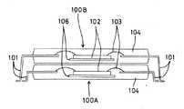
ところで、図6および図7には、上記のような従来の工法により製造された積層パッケージを示した。図6に示すものは、樹脂でモールドされたパッケージを積層したものである。また、図7は、図6のモジュール基板の平面図である。このICパッケージ100A、100Bには、IC実装部106と、その上面に実装されたICチップ102と、ICチップ102と外部部品とを接続するリード101と、ICチップ102とリード101とを樹脂内部で接続するボンディングワイヤ103とが設けられている。また、ICチップ102を含む所定の領域は、樹脂体104により被覆されている。
【0005】
このような構造のICパッケージ100Aの上側には、他のICパッケージ100Bが積層された状態とされて、基板105に実装されている。
【0006】
【発明が解決しようとする課題】
上記のICパッケージ100A、100Bを厚さ方向に積み重ねて、基板105に実装しようとすると、樹脂体104の厚みのために総モジュール厚が厚くなってしまうという問題がある。また、ICパッケージ100A、100Bを横方向に基板105に実装する場合には、総モジュールが大きくなるという問題がある。さらに、上下のパッケージ100A、100Bは、それぞれのリード101によって基板105に接続されているので、パッケージ100A、100Bの積層時に位置ずれが生じると、リード101間が短絡してしまう可能性があった。
【0007】
今後は、例えばICカードや携帯電話等の電子機器の小型化に伴い、ICパッケージに対しても、更なる高密度化と薄型化が図られると考えられているが、従来の工法によっては、そのような高密度・薄型化を図ることは困難である。
【0008】
この問題を解決するためには、ICチップ102を樹脂体104でモールドする構成を変更し、例えばプリント基板を層間部材を介して積層しながらその層間にICチップを実装するという構成が考えられる。そのような構成を採用した場合には、層間部材に形成させた導電性バンプによって、その表裏に配されるプリント基板の導体回路を電気的に接続することが必要である。
【0009】
しかしながら、これらのプリント基板及び層間部材を積層する際には、各プリント基板と層間部材との間に接着層を形成することが必要であるから、その接着層の存在によって層間部材の導電性バンプとプリント基板の導体回路の接触性が阻害され、接続信頼性が低下してしまうおそれがある。
【0010】
本発明は、上記した事情に鑑みてなされたものであり、その目的は、接続信頼性を高めることのできる積層型の半導体モジュールを製造できる方法を提供することにある。
【0011】
【課題を解決するための手段】
上記の課題を解決するための請求項1の発明に係る半導体モジュールの製造方法は、所定の配線回路を形成させて一面側に半導体チップを実装した複数枚のプリント基板を、前記配線回路に接続可能な導電性バンプと前記半導体チップを収容可能な開口部とを備えた層間部材を介して積層する半導体モジュールの製造方法であって、前記層間部材となる絶縁性基材の両面に接着層を形成する工程と、前記接着層に保護フィルムを貼り付ける工程と、前記絶縁性基材の所定の位置にスルーホールを形成する工程と、前記スルーホールに導電性ペーストを充填して前記導電性バンプを形成する工程と、前記保護フィルムを剥離して前記導電性バンプが前記保護フィルムの厚さ分だけ前記接着層の表面から突出するように形成する工程と、前記絶縁性基材に前記半導体チップを収容可能な前記開口部を形成する工程と、前記絶縁性基材と前記プリント基板とを交互に積層して接着するとともに、前記配線回路と前記導電性バンプとを両者の間に前記接着層を噛み込ませることなく接触させて接続する工程とを経ることを特徴とする。
【0012】
【発明の作用、および発明の効果】
請求項1の発明によれば、層間部材に導電性バンブを形成させる際には、まず絶縁性基板の両面に接着層を形成させ、この接着層の表面に保護フィルムを貼りつけておく。その後、所定の位置にスルーホールを形成させ、このスルーホールに導電性ペーストを充填した後に、保護フィルムを剥離する。これにより、導電性バンプは、保護フィルムの厚さ分だけ接着層の表面から突出するように形成される。このため、導電性バンプとプリント基板の導体回路との間に接着層が噛み込んで接触を阻害することを回避でき、接続信頼性を高めることができる。
【0013】
【発明の実施の形態】
以下、本発明を具体化した一実施形態について、図1〜図5を参照しつつ詳細に説明する。本実施形態の半導体モジュール1は、半導体チップ3を実装したプリント基板2と層間部材20と交互に重ね合わせ、最下層にI/O配線基板30を重ねて熱プレスすることにより一体化された構造となっている(図1参照)。
【0014】
まず、半導体チップ3を実装したプリント基板2の製造方法について説明する。
【0015】
プリント基板2の出発材料は、片面銅張積層板4である。この片面銅張積層板4は、例えば板状のガラス布エポキシ樹脂により形成される厚さ75μmの絶縁性基板5の一方の面(図3において上面)に、全面に厚さ12μmの銅箔6が貼り付けられた周知の構造である。この片面銅張積層板4において、銅箔6とは反対側の面をポリエチレンテレフタレート(PET)製の保護フィルム7で保護しておく(図2A)。
【0016】
この保護フィルム7が施されている面側(図2において下面側)から、所定の位置に例えばパルス発振型炭酸ガスレーザ加工装置によってレーザ照射を行うことにより、絶縁性基板5を貫通して銅箔6に達するビアホール8を形成する(図2B)。加工条件は、パルスエネルギーが0.5〜10.0mJ、パルス幅が1〜100μs、パルス間隔が0.5ms以上、ショット数が3〜50の範囲内であることが好ましい。次いで、このビアホール8の内部に残留する樹脂を取り除くためのデスミア処理を行う。その後、銅箔6面を保護フィルム7で保護しておき、銅箔6を一方の電極として電解メッキ法によってビアホール8内にメッキ導体9を形成させる(図2C)。なお、メッキ導体9の充填深さは、その上面が保護フィルム7の表面と面一になる程度が好ましい。
【0017】
次に、銅箔6側の保護フィルム7を剥離した後に、感光性のドライフィルム10を貼りつける。このドライフィルム10を所定のパターンにより露光・現像処理することにより、孔部11を形成する(図2D)。この孔部11内に電解メッキを施すことにより、半導体チップ3を実装するための実装用バンプ12となるメッキ層を形成する(図2E)。
【0018】
その後、ドライフィルム10を剥離し、実装用バンプ12を突出させる。同時に、下面側の保護フィルム7を剥離することで、メッキ導体9の先端部が絶縁性基板5の表面から突出されて接続用バンプ13とされる(図3F)。
【0019】
次いで、電着法により、上面側全面と下面側の接続用バンプ13上にフォトレジスト層14を形成させる(図3G)。次に、上面側のフォトレジスト層14を所定の配線回路15のパターンに合わせて露光・現像処理する。この後、フォトレジスト層14により保護されていない銅箔6部分をエッチング処理することにより、配線回路15を形成させる(図3H)。配線回路15の一部は、後述する層間部材20の導電性バンプ26と接続するための接続用ランド15Aとされている。最後に、フォトレジスト層14を除去することにより、プリント基板2の製造が完了する(図3I)。
【0020】
このプリント基板2の上面側の中央部分には、半導体チップ3が実装される(図3J)。半導体チップ3は、プリント基板2の中央に接着剤16により固着され、半導体チップ3の下面側に形成された端子部(図示せず)が実装用バンプ12に埋め込まれることにより、プリント基板2の配線回路15と電気的に接続される。
【0021】
次に、層間部材20の製造方法について説明する。
【0022】
層間部材20の出発材料は、板状のガラス布基材エポキシ樹脂により形成される絶縁性基材21である(図4A)。この絶縁性基材21の厚さは、後述のキャビティ(本発明の開口部に該当する)27内に半導体チップ3を収容する必要性から、プリント基板2の上面から半導体チップ3の上面までの高さよりもやや厚く、例えば130μmとされている。また、絶縁性基材21の上面および下面の面積は対向するプリント基板2の面積と略等しくされている。
【0023】
この絶縁性基材21の両面に接着層22を形成させておき、さらにその上面をPET製の保護フィルム23で保護しておく(図4B)。次いで、保護フィルム23の上から、対向するプリント基板2の接続用ランド15Aおよび接続用バンプ13に対応する位置に、例えばパルス発振型炭酸ガスレーザ加工装置によってレーザ照射を行うことにより、絶縁性基材21の厚さ方向に貫通するスルーホール24を形成させる(図4C)。
【0024】
このスルーホール24内に、導電性ペースト25を充填する(図4D)。充填は、例えばスクリーン印刷機により導電性ペースト25を保護フィルム23上から印刷することにより行うことができる。そして、保護フィルム23を剥離すると、導電性ペースト25は保護フィルム23の厚さ分だけ接着層22の表面から突出されて導電性バンプ26とされる(図4E)。
【0025】
そして、絶縁性基材21の中央部分に、例えばレーザ照射を行うことによりキャビティ27を貫通形成させて、層間部材20の製造が完了する(図4F)。キャビティ27の大きさは半導体チップ3の外形寸法よりやや大きくされて、その内部に半導体チップ3を収容可能とされている。
【0026】
上記のように製造されたプリント基板2と層間部材20とを交互に重ね合わせる(図5A)。このとき、最上層にはプリント基板2が、半導体チップ3を実装された面が下面側になるように配置され、その下方には層間部材20が配置される。層間部材20は、そのキャビティ27内にプリント基板2の半導体チップ3を収容し、また、導電性バンプ26がプリント基板2の接続用ランド15Aおよび接続用バンプ13と接続可能なように重ね合わせられる。そして、その下方にはさらにプリント基板2および層間部材20が同様に重ね合わせられ、最下層にはI/O配線基板30が積層される。このI/O配線基板30は、絶縁性基板33の所定の位置にビアホール34が形成され、その上下に所定の配線回路(図示せず)およびランド31が形成されたものである。
【0027】
次いで、加熱真空プレスすることによって、接着層22が硬化して上下のプリント基板2およびI/O配線基板30と接着し、半導体モジュール1が形成される(図5B)。そして、層間部材20に形成されたスルーホール24により、上下のプリント基板2およびI/O配線基板30の配線回路間が電気的に接続される。このとき、各プリント基板2の接続用ランド15A、接続用パンプ13、およびI/O配線基板30のランド31と、隣接する層間部材20の導電性バンプ26とが接続されており、これにより上下のプリント基板2およびI/O配線基板30の配線回路間が電気的に接続される。また、 I/O配線基板30の下面側のランド31には、外部基板との接続用のはんだボール32が形成される。
【0028】
以上のように本実施形態によれば、層間部材20に導電性バンプ26を形成する際には、まず絶縁性基板21の両面に接着層22を形成させ、この接着層22の表面に保護フィルム23を貼りつけておく。その後、所定の位置にスルーホール24を形成させ、このスルーホール24に導電性ペースト25を充填した後に、保護フィルム23を剥離する。このため、導電性バンプ26は、保護フィルム23の厚さ分だけ接着層22の表面から突出するように形成される。これにより、層間部材20をプリント基板2およびI/O配線基板30とともに積層する際に、接続用ランド15A、ランド31と導電性バンプ26との接触性が接着層22によって阻害されることがなく、接続信頼性を高めることができる。
【0029】
なお、本発明の技術的範囲は、上記した実施形態によって限定されるものではなく、例えば、次に記載するようなものも本発明の技術的範囲に含まれる。その他、本発明の技術的範囲は、均等の範囲にまで及ぶものである。
(1)本実施形態では、層間部材20の出発材料としてガラス布基材エポキシ樹脂製の絶縁性基材21を使用したが、本発明によれば絶縁性基材の材質は上記実施形態の限りではなく、例えば紙基材フェノール樹脂や、合成繊維布基材エポキシ樹脂であってもよい。
(2)本実施形態では、I/O配線基板30の下面側には外部基板との接続用のはんだボール32が形成されているが、本発明によれば半導体モジュールと外部基板との接続は上記実施形態の限りではなく、例えば導電性のピンが用いられていてもよい。
(3)本実施形態では、キャビティ27は導電性バンプ26の形成後に形成されているが、本発明によればキャビティの形成は上記実施形態の限りではなく、例えばスルーホールの形成と同時に行ってもよい。また、スルーホールの形成前に行ってもよい。
【図面の簡単な説明】
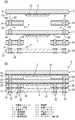
【図1】本実施形態におけるプリント基板と層間部材とを積層させて多層プリント配線板を製造する前の様子を示す斜視図
【図2】プリント基板の製造方法を示す断面図−1
【図3】プリント基板の製造方法を示す断面図−2
【図4】層間部材の製造方法を示す断面図
【図5】プリント基板と層間部材とを積層させて半導体モジュールを形成した断面図
【図6】従来におけるICパッケージの側断面図
【図7】(a)従来におけるICパッケージを実装した基板の側面図
(b)従来におけるICパッケージを実装した基板の平面図
【符号の説明】
1…半導体モジュール
2…プリント基板
3…半導体チップ
15…配線回路
20…層間部材
21…絶縁性基材
22…接着層
23…保護フィルム
24…スルーホール
25…導電性ペースト
26…導電性バンプ
27…キャビティ(開口部)[0001]
BACKGROUND OF THE INVENTION
The present invention relates to a method for manufacturing a semiconductor module.
[0002]
[Prior art]
In recent years, in order to cope with high-density mounting of IC chips, a technique for manufacturing a semiconductor module in which IC chips are stacked has been developed. For example, JP-A-9-219490, JP-A-10-135267, and JP-A-10-163414 disclose such a stacked package.
[0003]
In such a conventional technique, IC packages such as TSOP (Thin Small Outline Package), TCP (Tape Carrier Package), and BGA (Ball Grid Array) are assembled for each layer, and then a plurality of IC packages are stacked. At this time, the respective layers are connected via external connection terminals provided in advance in each package. Thus, in the conventional construction method, since many manufacturing steps have to be performed, the processing cost has increased.
[0004]
6 and 7 show a stacked package manufactured by the conventional method as described above. The one shown in FIG. 6 is a laminate of packages molded with resin. FIG. 7 is a plan view of the module substrate of FIG. The
[0005]
Another
[0006]
[Problems to be solved by the invention]
If the
[0007]
In the future, for example, with the miniaturization of electronic devices such as IC cards and mobile phones, it is considered that further increases in density and thickness will be achieved for IC packages, but depending on the conventional construction method, It is difficult to achieve such high density and thinning.
[0008]
In order to solve this problem, a configuration in which the
[0009]
However, when laminating these printed circuit boards and interlayer members, it is necessary to form an adhesive layer between each printed circuit board and the interlayer member. There is a risk that the contact reliability of the conductor circuit of the printed circuit board is hindered and the connection reliability is lowered.
[0010]
The present invention has been made in view of the above-described circumstances, and an object of the present invention is to provide a method capable of manufacturing a stacked semiconductor module capable of improving connection reliability.
[0011]
[Means for Solving the Problems]
According to a first aspect of the present invention, there is provided a method for manufacturing a semiconductor module, comprising: connecting a plurality of printed circuit boards having a predetermined wiring circuit formed thereon and mounting a semiconductor chip on one side thereof to the wiring circuit; A method of manufacturing a semiconductor module, which is laminated via an interlayer member provided with possible conductive bumps and an opening capable of accommodating the semiconductor chip, wherein adhesive layers are formed on both surfaces of the insulating base material to be the interlayer member A step of forming, a step of attaching a protective film to the adhesive layer, a step of forming a through hole at a predetermined position of the insulating base, and a conductive paste filling the through hole to form the conductive bump forming, andforming as the protective film peelingto the conductive bump protrudes from the surface of only the thickness of the adhesive layer of the protective film, the insulatingBoth forming said opening capable of accommodating the semiconductor chip to a substrate, theaddition to the adhesive insulating base material and the said printed circuit board by laminatingalternately with said conductive bump and the wiring circuit And the step of contacting andconnecting the adhesive layer without biting between them.
[0012]
Operation of the invention and effect of the invention
According to the first aspect of the present invention, when the conductive bump is formed on the interlayer member, an adhesive layer is first formed on both surfaces of the insulating substrate, and a protective film is pasted on the surface of the adhesive layer. Thereafter, a through hole is formed at a predetermined position, and after filling the through hole with a conductive paste, the protective film is peeled off. Thus, the conductive bump is formed so as to protrude from the surface of the adhesive layer by the thickness of the protective film. For this reason, it can avoid that an adhesive layer bites between a conductive bump and the conductor circuit of a printed circuit board, and a contact is inhibited, and can improve connection reliability.
[0013]
DETAILED DESCRIPTION OF THE INVENTION
DESCRIPTION OF EMBODIMENTS Hereinafter, an embodiment embodying the present invention will be described in detail with reference to FIGS. The
[0014]
First, a method for manufacturing the printed
[0015]
The starting material for the printed
[0016]
From the surface side on which the
[0017]
Next, after peeling off the
[0018]
Thereafter, the
[0019]
Next, a
[0020]
A
[0021]
Next, a method for manufacturing the
[0022]
The starting material of the
[0023]
The
[0024]
The through-
[0025]
Then, the
[0026]
The printed
[0027]
Next, by heating and vacuum pressing, the
[0028]
As described above, according to the present embodiment, when forming the
[0029]
The technical scope of the present invention is not limited by the above-described embodiment, and for example, the following are also included in the technical scope of the present invention. In addition, the technical scope of the present invention extends to an equivalent range.
(1) In this embodiment, the insulating
(2) In this embodiment, the
(3) In this embodiment, the
[Brief description of the drawings]
FIG. 1 is a perspective view showing a state before a multilayer printed wiring board is manufactured by laminating a printed board and an interlayer member in the present embodiment. FIG. 2 is a cross-sectional view showing a method for manufacturing a printed board.
FIG. 3 is a cross-sectional view showing a method for manufacturing a printed circuit board-2.
4 is a cross-sectional view showing a method for manufacturing an interlayer member. FIG. 5 is a cross-sectional view in which a printed circuit board and an interlayer member are stacked to form a semiconductor module. FIG. 6 is a side cross-sectional view of a conventional IC package. (A) Side view of a substrate on which a conventional IC package is mounted (b) Plan view of a substrate on which a conventional IC package is mounted
DESCRIPTION OF
Claims (1)
Translated fromJapanesePriority Applications (2)
| Application Number | Priority Date | Filing Date | Title |
|---|---|---|---|
| JP2000242992AJP4550239B2 (en) | 2000-08-10 | 2000-08-10 | Manufacturing method of semiconductor module |
| TW91102404ATW543083B (en) | 2000-08-10 | 2002-02-08 | Method for manufacturing semiconductor module |
Applications Claiming Priority (1)
| Application Number | Priority Date | Filing Date | Title |
|---|---|---|---|
| JP2000242992AJP4550239B2 (en) | 2000-08-10 | 2000-08-10 | Manufacturing method of semiconductor module |
Publications (2)
| Publication Number | Publication Date |
|---|---|
| JP2002057275A JP2002057275A (en) | 2002-02-22 |
| JP4550239B2true JP4550239B2 (en) | 2010-09-22 |
Family
ID=18733920
Family Applications (1)
| Application Number | Title | Priority Date | Filing Date |
|---|---|---|---|
| JP2000242992AExpired - Fee RelatedJP4550239B2 (en) | 2000-08-10 | 2000-08-10 | Manufacturing method of semiconductor module |
Country Status (1)
| Country | Link |
|---|---|
| JP (1) | JP4550239B2 (en) |
Families Citing this family (1)
| Publication number | Priority date | Publication date | Assignee | Title |
|---|---|---|---|---|
| JP4643055B2 (en)* | 2001-05-02 | 2011-03-02 | 新藤電子工業株式会社 | TAB tape carrier manufacturing method |
Family Cites Families (6)
| Publication number | Priority date | Publication date | Assignee | Title |
|---|---|---|---|---|
| JPS6079770U (en)* | 1983-11-07 | 1985-06-03 | 関西日本電気株式会社 | Stacked hybrid IC |
| JPH0559873U (en)* | 1992-01-14 | 1993-08-06 | 株式会社村田製作所 | 3D circuit board |
| JPH10190159A (en)* | 1996-12-24 | 1998-07-21 | Matsushita Electric Ind Co Ltd | Printed base material, circuit board connecting material using the same, and method of manufacturing multilayer circuit board using the circuit board connecting material |
| JP2870528B1 (en)* | 1997-10-01 | 1999-03-17 | 日本電気株式会社 | 3D memory module |
| JP4051769B2 (en)* | 1998-06-22 | 2008-02-27 | 松下電器産業株式会社 | Circuit forming substrate manufacturing method, manufacturing apparatus therefor, and circuit forming substrate material |
| JP2001177051A (en)* | 1999-12-20 | 2001-06-29 | Toshiba Corp | Semiconductor device and system device |
- 2000
- 2000-08-10JPJP2000242992Apatent/JP4550239B2/ennot_activeExpired - Fee Related
Also Published As
| Publication number | Publication date |
|---|---|
| JP2002057275A (en) | 2002-02-22 |
Similar Documents
| Publication | Publication Date | Title |
|---|---|---|
| US8749073B2 (en) | Wiring board, method of manufacturing the same, and semiconductor device | |
| US7029953B2 (en) | Semiconductor package for three-dimensional mounting, fabrication method thereof, and semiconductor device | |
| CN100435299C (en) | Manufacturing method of wiring substrate | |
| JP3670917B2 (en) | Semiconductor device and manufacturing method thereof | |
| JP4248761B2 (en) | Semiconductor package, manufacturing method thereof, and semiconductor device | |
| KR101344800B1 (en) | Wiring board and semiconductor device | |
| KR101168263B1 (en) | Semiconductor package and fabrication method thereof | |
| US20110314667A1 (en) | Method of manufacturing printed circuit board including electronic component embedded therein | |
| JP2016063130A (en) | Printed wiring board and semiconductor package | |
| TWI506758B (en) | Package on package structure and method for manufacturing same | |
| WO2015083345A1 (en) | Wiring board with embedded components and manufacturing method thereof | |
| JP2015211194A (en) | Printed wiring board, semiconductor package and printed wiring board manufacturing method | |
| JP4954765B2 (en) | Wiring board manufacturing method | |
| JP4022405B2 (en) | Circuit board for mounting semiconductor chips | |
| US7358591B2 (en) | Capacitor device and semiconductor device having the same, and capacitor device manufacturing method | |
| KR100346899B1 (en) | A Semiconductor device and a method of making the same | |
| JP4376891B2 (en) | Semiconductor module | |
| JP4365515B2 (en) | Manufacturing method of semiconductor module | |
| JP4550239B2 (en) | Manufacturing method of semiconductor module | |
| JP4562881B2 (en) | Manufacturing method of semiconductor module | |
| JP4562153B2 (en) | Manufacturing method of semiconductor module | |
| JP2015109346A (en) | Component incorporated wiring board and manufacturing method thereof | |
| JP4410370B2 (en) | Multilayer circuit board | |
| JP4376890B2 (en) | Circuit board for mounting semiconductor chips | |
| JP4562154B2 (en) | Manufacturing method of semiconductor module |
Legal Events
| Date | Code | Title | Description |
|---|---|---|---|
| RD04 | Notification of resignation of power of attorney | Free format text:JAPANESE INTERMEDIATE CODE: A7424 Effective date:20010517 | |
| RD04 | Notification of resignation of power of attorney | Free format text:JAPANESE INTERMEDIATE CODE: A7424 Effective date:20010518 | |
| A521 | Request for written amendment filed | Free format text:JAPANESE INTERMEDIATE CODE: A821 Effective date:20010730 | |
| RD02 | Notification of acceptance of power of attorney | Free format text:JAPANESE INTERMEDIATE CODE: A7422 Effective date:20010730 | |
| RD04 | Notification of resignation of power of attorney | Free format text:JAPANESE INTERMEDIATE CODE: A7424 Effective date:20061201 | |
| A621 | Written request for application examination | Free format text:JAPANESE INTERMEDIATE CODE: A621 Effective date:20070717 | |
| RD02 | Notification of acceptance of power of attorney | Free format text:JAPANESE INTERMEDIATE CODE: A7422 Effective date:20090909 | |
| RD04 | Notification of resignation of power of attorney | Free format text:JAPANESE INTERMEDIATE CODE: A7424 Effective date:20090909 | |
| A131 | Notification of reasons for refusal | Free format text:JAPANESE INTERMEDIATE CODE: A131 Effective date:20100506 | |
| A521 | Request for written amendment filed | Free format text:JAPANESE INTERMEDIATE CODE: A523 Effective date:20100616 | |
| TRDD | Decision of grant or rejection written | ||
| A01 | Written decision to grant a patent or to grant a registration (utility model) | Free format text:JAPANESE INTERMEDIATE CODE: A01 Effective date:20100706 | |
| A01 | Written decision to grant a patent or to grant a registration (utility model) | Free format text:JAPANESE INTERMEDIATE CODE: A01 | |
| A61 | First payment of annual fees (during grant procedure) | Free format text:JAPANESE INTERMEDIATE CODE: A61 Effective date:20100708 | |
| R150 | Certificate of patent or registration of utility model | Ref document number:4550239 Country of ref document:JP Free format text:JAPANESE INTERMEDIATE CODE: R150 Free format text:JAPANESE INTERMEDIATE CODE: R150 | |
| FPAY | Renewal fee payment (event date is renewal date of database) | Free format text:PAYMENT UNTIL: 20130716 Year of fee payment:3 | |
| R250 | Receipt of annual fees | Free format text:JAPANESE INTERMEDIATE CODE: R250 | |
| R250 | Receipt of annual fees | Free format text:JAPANESE INTERMEDIATE CODE: R250 | |
| R250 | Receipt of annual fees | Free format text:JAPANESE INTERMEDIATE CODE: R250 | |
| LAPS | Cancellation because of no payment of annual fees |