JP4547847B2 - Discharge lamp lighting device - Google Patents
Discharge lamp lighting deviceDownload PDFInfo
- Publication number
- JP4547847B2 JP4547847B2JP2001302775AJP2001302775AJP4547847B2JP 4547847 B2JP4547847 B2JP 4547847B2JP 2001302775 AJP2001302775 AJP 2001302775AJP 2001302775 AJP2001302775 AJP 2001302775AJP 4547847 B2JP4547847 B2JP 4547847B2
- Authority
- JP
- Japan
- Prior art keywords
- power supply
- output
- discharge lamp
- control power
- capacitor
- Prior art date
- Legal status (The legal status is an assumption and is not a legal conclusion. Google has not performed a legal analysis and makes no representation as to the accuracy of the status listed.)
- Expired - Fee Related
Links
Images


Classifications
- Y—GENERAL TAGGING OF NEW TECHNOLOGICAL DEVELOPMENTS; GENERAL TAGGING OF CROSS-SECTIONAL TECHNOLOGIES SPANNING OVER SEVERAL SECTIONS OF THE IPC; TECHNICAL SUBJECTS COVERED BY FORMER USPC CROSS-REFERENCE ART COLLECTIONS [XRACs] AND DIGESTS
- Y02—TECHNOLOGIES OR APPLICATIONS FOR MITIGATION OR ADAPTATION AGAINST CLIMATE CHANGE
- Y02B—CLIMATE CHANGE MITIGATION TECHNOLOGIES RELATED TO BUILDINGS, e.g. HOUSING, HOUSE APPLIANCES OR RELATED END-USER APPLICATIONS
- Y02B20/00—Energy efficient lighting technologies, e.g. halogen lamps or gas discharge lamps
Landscapes
- Circuit Arrangements For Discharge Lamps (AREA)
- Discharge-Lamp Control Circuits And Pulse- Feed Circuits (AREA)
Description
Translated fromJapanese【0001】
【発明の属する技術分野】
本発明は、高周波インバータを用いて放電灯を高周波で点灯または調光する放電灯点灯装置に関するものである。
【0002】
【従来の技術】
従来、放電灯点灯装置においては、入力歪改善回路またはインバータ回路などに含まれるFETなどのスイッチング素子を高周波で駆動する制御回路(制御ICなど)が広く用いられている。
【0003】
この制御回路には、これに安定した電源を供給するための制御電源がインバータ回路の電源とは別に必要となる。制御電源の電圧は通常15V程度のことが多く、制御回路に必要とされる電流もその仕様により決まる。放電灯点灯装置の場合、制御電源は、電源電圧の状態、放電灯の定格電力の種類、または予熱時、始動時、調光時における放電灯の状態に関わらず、電圧および電流を制御回路に安定して供給しなければならない。
【0004】
図7に従来の高周波用の放電灯点灯装置のブロック図を示し、図8から図11に同放電灯点灯装置に使用される各種制御電源の回路構成を示し、調光機能が付加されていない放電灯点灯装置の制御回路のための制御電源について説明する。
【0005】
図7に示す放電灯点灯装置は、交流電源11と、この交流電源11からの交流電圧Vinを整流平滑する整流平滑回路Aと、入力歪み改善機能を備えた直流電源回路(チョッパ回路)Bと、この直流電源回路Bから供給される出力電圧Vdcを交流電圧に変換する高周波変換回路(インバータ)Cと、共振回路Dと、この共振回路Dを介して高周波変換回路Cで変換された交流電圧が供給され点灯する放電灯Laとを備えている。
【0006】
ここで、図8の例に示すように、高周波変換回路Cとして、スイッチング素子Q1,Q2、直流カット用コンデンサC2および制御回路20を含むインバータ2を備え、共振回路Dとして、共振用インダクタL1および共振用コンデンサC1を備える放電灯点灯装置では、制御回路20用として、電解コンデンサC3、抵抗R41、ダイオードD41および2次巻線n41により構成される制御電源4が設けられる場合がある。制御電源4の出力となる電解コンデンサC3のプラス端子は制御回路20に接続されており、電解コンデンサC3は、ダイオードD41および抵抗R41を介して、共振用インダクタL1に設けられた2次巻線n41に発生する誘起電圧が印加することにより充電される。
【0007】
図9の例に示すように、インバータ2を図8と同様に備える放電灯点灯装置では、制御回路20用として、電解コンデンサC3、抵抗R41、ダイオードD41,D42およびコンデンサC41により構成される制御電源4aが設けられる場合もある。この場合の構成も、電解コンデンサC3のプラス端子が制御回路20に接続されているが、電解コンデンサC3は、コンデンサC41およびダイオードD41の接続点からダイオードD41および抵抗R41を介して電圧が印加することにより充電される。
【0008】
図10の例に示すように、直流電源回路Bとして、スイッチング素子Q11、ダイオードD11、インダクタL11、平滑コンデンサC11および制御回路12aにより構成されるチョッパ(同図では降圧チョッパ)10を備える放電灯点灯装置では、制御回路12a用として、電解コンデンサC3、抵抗R41、ダイオードD41および2次巻線n42により構成される制御電源4bが設けられることがある。制御電源4bの出力となる電解コンデンサC3のプラス端子は制御回路12aに接続されており、電解コンデンサC3は、ダイオードD41および抵抗R41を介して、インダクタL11に設けられた2次巻線n42に発生する誘起電圧が印加することにより充電される。なお、制御回路12aは、PWM−ICであり、スイッチング素子Q11はオンデューティ可変となっている。
【0009】
図11の例に示すように、インバータ2、共振用インダクタL1および共振用コンデンサC1を図8と同様に備える放電灯点灯装置では、制御回路20用として、電解コンデンサC3および抵抗R42〜R44により構成される制御電源4cが設けられることもある。この構成でも、電解コンデンサC3のプラス端子が制御回路20に接続されているが、電解コンデンサC3は、整流平滑回路Aの出力電圧が抵抗R42〜R44により分圧されて印加することにより充電される。
【0010】
以上のように、調光機能を備えていない(例えば定格出力のみの)放電灯点灯装置では、電解コンデンサC3への電流量が変化しないため、制御回路に安定した電圧を供給することができる。
【0011】
なお、特開2000−48988公報には、始動時には、他励制御回路への電路インピーダンスを高くし、通常点灯時には、他励制御回路への電路インピーダンスを低くすることにより、あるいは放電灯が点灯した後の他励制御回路の電源不足が生じないように、始動時周波数と点灯時周波数を同じとすることにより、始動時の制御電源へのストレスや点灯後の制御電源の低下を防止するようにした放電灯点灯装置が開示されている。
【0012】
【発明が解決しようとする課題】
しかしながら、上記図8〜図11に示した回路構成の制御電源では、放電灯Laの電圧Vlaが変化する場合や、直流電源の出力電圧Vdcが可変である場合、制御回路に電圧を安定して供給することができない課題がある。
【0013】
図8の制御電源では、放電灯Laの電圧Vlaまたは直流電源回路Bの出力電圧Vdcが変化すると、インダクタL1の電圧が変化するので、その2次巻線n41の電圧も変化して、電解コンデンサC3の充電電圧が変化することになり、制御電源4は、制御回路20に電圧を安定して供給することができなくなる。
【0014】
図9の制御電源では、直流電源回路Bの出力電圧Vdcが変化すると、スイッチング素子Q2の両端電圧が変化するので、電解コンデンサC3の充電電圧が変化することになり、制御電源4aは、制御回路20に電圧を安定して供給することができなくなる。
【0015】
図10の制御電源では、交流電源11の交流電圧Vinまたはチョッパ10の出力電圧Vdcが変化する場合、インダクタL11の電圧が変化するので、その2次巻線n42の電圧も変化して、電解コンデンサC3の充電電圧が変化することになり、制御電源4bは、制御回路12aに電圧を安定して供給することができなくなる。
【0016】
図11の制御電源では、交流電源11の交流電圧Vinが一定である場合、制御電源4cは、制御回路20に電圧を安定して供給することができるが、交流電圧Vinの例えば実効値が変化する用途には、制御電源4cを使用することができない。また、分圧用の抵抗が常時接続されることにより、電力ロスが発生し、回路の効率が低下する。
【0017】
ここで、上記のような放電灯点灯装置において、直流電源の出力電圧Vdcのレベルを調整することにより、放電灯Laを調光する場合があるが、図8〜図10に示した回路構成の制御電源では、図12に示すように、電解コンデンサC3の電圧が直流電源の出力電圧Vdcのレベル調整に応じて変動し、制御回路の安定動作に必要なV1〜V2の電圧範囲を外れることになる。これでは、放電灯Laの点灯を維持することができない。
【0018】
本発明は、上記事情に鑑みてなされたものであり、直流電源の出力電源が可変であっても、電源電圧を抵抗で分圧することなく、制御回路用の制御電源の出力を安定にすることができる放電灯点灯装置を提供することを目的とする。
【0019】
【課題を解決するための手段】
上記課題を解決するための請求項1記載の発明の放電灯点灯装置は、出力電源可変の直流電源と、スイッチング素子を含み前記直流電源の出力に接続されたインバータと、共振用インダクタと、この共振用インダクタを介して前記インバータの出力に接続された共振用コンデンサと、この共振用コンデンサと並列に接続された放電灯とを備え、前記直流電源およびインバータの少なくとも一方に含まれるスイッチング素子を高周波で駆動させる制御回路のための制御電源を、前記直流電源の出力の増加に応じて、出力が増加する第1の制御電源供給手段と、前記直流電源の出力の増加に応じて、出力が減少する第2の制御電源供給手段とにより構成してなり、前記インバータは、第1のスイッチング素子と、この第1のスイッチング素子を介して前記直流電源の出力に接続された第2のスイッチング素子と、これら第1および第2のスイッチング素子の接続点と前記共振用インダクタとの間に介設された直流カット用コンデンサとを含み、前記第1の制御電源供給手段は、前記第1および第2のスイッチング素子のうち接地側のスイッチング素子と並列に接続されていることを特徴とする。
【0023】
請求項2記載の発明は、請求項1記載の放電灯点灯装置において、前記放電灯は、前記直流電源の出力の増加に応じて電圧が下降し、前記第2の制御電源供給手段は前記放電灯と並列に接続されていることを特徴とする。
【0024】
請求項3記載の発明は、請求項1記載の放電灯点灯装置において、前記制御電源は、この制御電源の出力側に前記制御回路に接続される電解コンデンサを有し、前記第2の制御電源供給手段は、コンデンサと、前記コンデンサに直列に接続されるツェナーダイオードと、一端が前記コンデンサと前記ツェナーダイオードとの中点に接続され他端が前記電解コンデンサに接続されるダイオードと、前記コンデンサおよび前記ツェナーダイオードと並列に接続される前記共振用コンデンサを含むことを特徴とする。
【0025】
請求項4記載の発明は、請求項1記載の放電灯点灯装置において、前記第1および第2の制御電源供給手段の少なくとも一方にはスイッチが接続されていることを特徴とする。
【0026】
請求項5記載の発明は、請求項4記載の放電灯点灯装置において、前記第1および第2の制御電源供給手段の少なくとも一方に接続されているスイッチは、前記直流電源の出力に応じてオン/オフすることを特徴とする。
【0027】
【発明の実施の形態】
(基本形態)
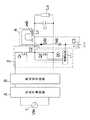
図1は基本形態の放電灯点灯装置の回路構成図、図2は図1中の制御電源の出力電圧の説明図であり、これらの図を参照しながら基本形態について説明する。
【0028】
本基本形態の放電灯点灯装置は、図1に示すように、出力電源可変の直流電源1と、この直流電源1の出力に接続され制御回路20を含むインバータ2と、共振用インダクタL1と、この共振用インダクタL1を介してインバータ2の出力に接続された共振用コンデンサC1と、この共振用コンデンサC1と並列に接続された放電灯Laと、制御回路20のための制御電源3とを備え、直流電源1の出力電圧Vdcのレベルを変更することにより調光を行う機能を有している。
【0029】
図1の例では、インバータ2は、スイッチング素子Q1と、このスイッチング素子Q1を介して直流電源1の出力に接続されたスイッチング素子Q2と、これらスイッチング素子Q1,Q2の接続点と共振用インダクタL1との間に介設された直流カット用コンデンサC2とをさらに含み、上述の制御回路20によりスイッチング素子Q1,Q2のオン/オフ制御を高周波で行う構成になっている。制御回路20は例えばPWM−ICであり、スイッチング素子Q1,Q2のスイッチング周波数は可変となっている。また、スイッチング素子Q1,Q2には、逆並列接続のダイオードを有する構造のFETが使用されている。
【0030】
制御電源3は、第1の制御電源4と、第2の制御電源5とを備え、これら双方で出力の電解コンデンサC3を共用する構成になっている。すなわち、電解コンデンサC3のプラス端子が制御電源3の出力として制御回路20に接続されている。
【0031】
そして、制御電源4は、電解コンデンサC3のプラス端子に一端が接続された抵抗R41と、この抵抗R41の他端にカソードが接続されたダイオードD41と、共振用インダクタL1に設けられ、ダイオードD41のアノードと電解コンデンサC3のマイナス端子(図1では接地されている)との間に介設された2次巻線n41とを備え、直流電源1の出力の増加(減少)に応じて、電解コンデンサC3における出力成分が増加(減少)する構成になっている。
【0032】
制御電源5は、電解コンデンサC3のプラス端子に一端が接続された抵抗R51と、この抵抗R51の他端にカソードが接続されたダイオードD51と、このダイオードD51のアノードにカソードが接続されたダイオードD52と、このダイオードD52を介して共振用コンデンサC1の両端に接続されたコンデンサC51とを備え、直流電源1の出力の増加(減少)に応じて、電解コンデンサC3における出力成分が減少(増加)する構成になっている。
【0033】
上記構成の放電灯点灯装置では、制御電源3中の制御電源4において、図2に示すように、直流電源1の出力電圧Vdcが“Dim”側から“Full”側に上昇すると、共振用インダクタL1の電圧が上昇することにより、その2次巻線n41の誘起電圧が上昇し、この2次巻線n41からダイオードD41および抵抗R41を介して電解コンデンサC3のプラス端子に供給される電流が増大する。逆に、直流電源1の出力電圧Vdcが“Full”側から“Dim”側に下降すると、共振用インダクタL1の電圧が下降することにより、2次巻線n41の誘起電圧が下降し、この2次巻線n41から電解コンデンサC3のプラス端子に供給される電流が減少する。
【0034】
他方、制御電源5においては、直流電源1の出力電圧Vdcが“Dim”側から“Full”側に上昇すると、放電灯Laの電圧Vlaが下降するために、コンデンサC51およびダイオードD51の接続点からダイオードD51および抵抗R51を介して電解コンデンサC3のプラス端子に供給される電流が減少する。逆に、直流電源1の出力電圧Vdcが“Full”側から“Dim”側に下降すると、放電灯Laの電圧Vlaが上昇するために、電解コンデンサC3のプラス端子に供給される電流が増大する。
【0035】
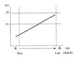
つまり、制御電源4においては、図2の“V4”に示すように、直流電源1の出力の増加(減少)に応じて、電解コンデンサC3における出力成分が増加(減少)する一方で、制御電源5においては、図2の“V5”に示すように、直流電源1の出力の増加(減少)に応じて、電解コンデンサC3における出力成分が減少(増加)するのである。これにより、直流電源1の出力電圧Vdcのレベルを変更することによる調光およびフル点灯の全体に亘って、制御電源3の出力である電解コンデンサC3の電圧が、図2の“V3”に示すように、ほぼ一定に保持されることになる。なお、図2中のV1およびV2は、それぞれ制御回路20の安定動作に必要な下限電圧および上限電圧を示す。
【0036】
(実施形態)
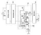
図3は本発明に係る実施形態の放電灯点灯装置の回路構成図であり、この図を参照しながら本実施形態について説明する。
【0037】
本実施形態の放電灯点灯装置は、図3に示すように、直流電源1と、インバータ2と、共振用インダクタL1と、共振用コンデンサC1と、放電灯Laとを基本形態と同様に備えているほか、基本形態との相違点として、制御電源3aを備えている。
【0038】
この制御電源3aは、第1の制御電源4aと、第2の制御電源5とを備え、これら双方で出力の電解コンデンサC3を共用する構成になっている。ここで、制御電源5については基本形態と同様であるのでその説明を省略し、基本形態の制御電源4とは異なる制御電源4aについて説明する。
【0039】
制御電源4aは、電解コンデンサC3のプラス端子に一端が接続された抵抗R41と、この抵抗R41の他端にカソードが接続されたダイオードD41と、このダイオードD41のアノードにカソードが接続されたダイオードD42と、このダイオードD42を介して、ソース接地のスイッチング素子Q2のドレイン・ソース間に接続されたコンデンサC41とを備え、直流電源1の出力の増加(減少)に応じて、電解コンデンサC3における出力成分が増加(減少)する構成になっている。
【0040】
上記構成の放電灯点灯装置では、制御電源3a中の制御電源4aにおいて、直流電源1の出力電圧Vdcが上昇すると、スイッチング素子Q2のドレイン・ソース間に発生する電圧が上昇することにより、コンデンサC41およびダイオードD41の接続点からダイオードD41および抵抗R41を介して電解コンデンサC3のプラス端子に供給される電流が増大する(図2の“V4”参照)。逆に、直流電源1の出力電圧Vdcが下降すると、スイッチング素子Q2のドレイン・ソース間に発生する電圧が下降することにより、電解コンデンサC3のプラス端子に供給される電流が減少する。
【0041】
したがって、制御電源5が基本形態と同様であるから、本実施形態でも、直流電源1の出力電圧Vdcのレベルを変更することによる調光およびフル点灯の全体に亘って、制御電源3aの出力である電解コンデンサC3の電圧がほぼ一定に保持されることになる。
【0042】
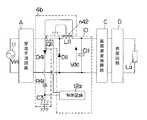
図4は他の放電灯点灯装置の回路構成図であり、この図を参照しながら説明する。
【0043】
図4の放電灯点灯装置は、インバータ2と、共振用インダクタL1と、共振用コンデンサC1と、放電灯Laとを基本形態と同様に備えているほか、基本形態との相違点として、直流電源1aと、制御電源3bとを備えている。
【0044】
直流電源1aは、交流電源11と、この交流電源11の交流電圧を直流電圧に整流する整流器DBと、この整流器DBの出力に接続された昇降圧チョッパとを備えている。その昇降圧チョッパは、整流器DBの負極性出力端子にアノードが接続されたダイオードD11と、このダイオードD11のカソードと整流器DBの正極性出力端子との間に接続されたスイッチング素子Q11と、ダイオードD11のカソードに一端が接続されたインダクタL11と、このインダクタL11の他端とダイオードD11のアノードとの間に接続されたスイッチング素子Q12と、インダクタL11の他端にアノードが接続されたダイオードD12と、このダイオードD12を介してスイッチング素子Q12の両端に接続された平滑コンデンサC11と、スイッチング素子Q11,Q12のオン/オフ制御を行う制御回路12とにより構成されている。この制御回路12は例えばPWM−ICであり、スイッチング素子Q11,Q12のオンデューティは可変となっている。
また、スイッチング素子Q11,Q12には、逆並列接続のダイオードを有する構造のFETが使用されている。
【0045】
ここで、上記昇降圧チョッパにおいて、平滑コンデンサC11の電圧が直流電源1aの出力電圧Vdcとなり、スイッチング素子Q11,Q12のスイッチング動作を調整することにより、昇圧機能を働かせて出力電圧Vdcを交流電源11のピーク電圧以上に昇圧することができるとともに、降圧機能を働かせて出力電圧Vdcを交流電源11のピーク電圧以下に降圧することができる。
【0046】
制御電源3bは、第1の制御電源4bと、第2の制御電源5とを備え、これら双方で出力の電解コンデンサC3を共用する構成になっている。すなわち、電解コンデンサC3のプラス端子が制御電源3bの出力として制御回路20,12の双方に接続されている。
【0047】
そして、制御電源5は基本形態と同様に構成されている一方、制御電源4bは、電解コンデンサC3のプラス端子に一端が接続された抵抗R41と、この抵抗R41の他端にカソードが接続されたダイオードD41と、インダクタL11に設けられ、ダイオードD41のアノードと電解コンデンサC3のマイナス端子との間に介設された2次巻線n42とにより構成されている。
【0048】
上記構成の放電灯点灯装置では、制御電源3b中の制御電源4bにおいて、直流電源1の出力電圧Vdcが上昇する場合には、インダクタL11の電圧が上昇して、その2次巻線n42の誘起電圧も上昇するので、2次巻線n42からダイオードD41および抵抗R41を介して電解コンデンサC3のプラス端子に供給される電流が増大する。逆に、直流電源1の出力電圧Vdcが下降する場合には、インダクタL11の電圧が下降して、その2次巻線n42の誘起電圧も下降するので、電解コンデンサC3のプラス端子に供給される電流が減少する。つまり、直流電源1の出力の増加(減少)に応じて、電解コンデンサC3における制御電源4bによる出力成分が増加(減少)するのである(図2の“V4”参照)。
【0049】
したがって、制御電源5が基本形態と同様であるから、参考例でも、直流電源1aの出力電圧Vdcのレベルを変更することによる調光およびフル点灯の全体に亘って、制御電源3bの出力である電解コンデンサC3の電圧がほぼ一定に保持されることになる。
【0050】
なお、上記基本形態、参考例および実施形態の構成を種々組み合わせることにより、同様な効果が得られることは言うまでもない。
【0051】
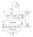
図5は他の放電灯点灯装置の回路構成図、図6は図5中の制御電源の出力電圧の説明図であり、これらの図を参照しながら説明する。
【0052】
図5の放電灯点灯装置は、直流電源1と、インバータ2と、共振用インダクタL1と、共振用コンデンサC1と、放電灯Laと、制御電源3とを基本形態と同様に備えているほか、基本形態との相違点としてVdc検出回路6を備えている。
【0053】
このVdc検出回路6は、抵抗R61〜R63を直列に接続して構成され直流電源1の出力と並列に接続される分圧回路と、直流電源61と、この直流電源61が反転入力端子に接続され上記分圧回路の出力(抵抗R63)が非反転入力端子に接続された比較器62と、第1の制御電源4における抵抗R41とダイオードD41との間に介設され比較器62の出力レベルがHigh(Low)のときにオン(オフ)になるスイッチSW1と、第2の制御電源5における抵抗R51とダイオードD51との間に介設され比較器62の出力レベルがLow(High)のときにオフ(オン)になるスイッチSW2とにより構成されている。
【0054】
上記構成の放電灯点灯装置では、直流電源1の出力電圧Vdcの分圧電圧(抵抗R63の電圧)が直流電源61の電圧E1を超えると、比較器60の出力レベルがHighとなり、スイッチSW1がオンになって制御電源4の機能が有効となるとともに、スイッチSW2がオフになって制御電源5の機能が無効となる。これにより、図6に示すように、直流電源1の出力電圧Vdcが直流電源61の電圧E1に対応する電圧Va以上になると、同図の“Va”から右側の“V3”のように、電圧V1からV2の範囲内において、制御電源3の出力である電解コンデンサC3の電圧が直流電源1の出力の増加(減少)に応じて増加(減少)する。
【0055】
これに対して、出力電圧Vdcの分圧電圧が電圧E1を下回ると、比較器62の出力レベルがLowとなり、スイッチSW1がオフになって制御電源4の機能が無効となるとともに、スイッチSW2がオンになって制御電源5の機能が有効となる。これにより、図6に示すように、出力電圧Vdcが電圧E1に対応する電圧Va以下になると、同図の“Va”から左側の“V3”のように、電圧V1からV2の範囲内において、制御電源3の出力である電解コンデンサC3の電圧が直流電源1の出力の増加(減少)に応じて減少(増加)する。
【0056】
したがって、図5の放電灯点灯装置では、直流電源1の出力電圧Vdcのレベルを変更することによる調光およびフル点灯の全体に亘って、制御電源3の出力である電解コンデンサC3の電圧が、制御回路20の安定動作に必要な下限電圧V1および上限電圧V2の範囲内に保持されることになる。
【0057】
また、スイッチSW1,SW2をオン/オフすることにより、2次巻線n41および抵抗R41,R51による電力ロスを低減することができる。
【0058】
さらに、直流電源1の出力電圧Vdcの変化により、制御電源3の出力が自動的に切り替わるので、連続調光に対応できる。
【0059】
なお、図5の放電灯点灯装置では、スイッチSW1,SW2を備える構成になっているが、これに限らず、どちらか一方のみを備える構成でもよい。この構成でも、同様な効果が得られるほか、コスト低減が可能となる。また、図5の放電灯点灯装置のスイッチSW1,SW2は、基本形態に限らず、参考例および図3の放電灯点灯装置にも適用可能であり、同様な効果が得られる。さらに、第2の制御電源に共振用コンデンサを含める構成でもよい。
【0060】
【発明の効果】
以上のことから明らかなように、請求項1記載の発明によれば、出力電源可変の直流電源と、スイッチング素子を含み前記直流電源の出力に接続されたインバータと、共振用インダクタと、この共振用インダクタを介して前記インバータの出力に接続された共振用コンデンサと、この共振用コンデンサと並列に接続された放電灯とを備え、前記直流電源およびインバータの少なくとも一方に含まれるスイッチング素子を高周波で駆動させる制御回路のための制御電源を、前記直流電源の出力の増加に応じて、出力が増加する第1の制御電源供給手段と、前記直流電源の出力の増加に応じて、出力が減少する第2の制御電源供給手段とにより構成してなり、前記インバータは、第1のスイッチング素子と、この第1のスイッチング素子を介して前記直流電源の出力に接続された第2のスイッチング素子と、これら第1および第2のスイッチング素子の接続点と前記共振用インダクタとの間に介設された直流カット用コンデンサとを含み、前記第1の制御電源供給手段は、前記第1および第2のスイッチング素子のうち接地側のスイッチング素子と並列に接続されているので、第1の制御電源供給手段の出力と第2の制御電源供給手段の出力とにより制御電源の全体としての出力を、例えば制御回路の許容動作電圧範囲内に収めることができるから、直流電源の可変出力を利用して放電灯を調光する場合でも、商用電源の整流および平滑により得られる電圧を分圧抵抗で分圧することなく、制御回路用の制御電源の出力を安定にすることができる。
【0063】
また、請求項1記載の発明によれば、第1の制御電源供給手段の出力が直流電源の出力の増加に応じて増加する一方、第2の制御電源供給手段の出力が直流電源の出力の増加に応じて減少するから、直流電源の可変出力を利用して放電灯を調光する場合、商用電源の電圧が異なる場合、そして放電灯の定格電力が異なる場合でも、制御回路用の制御電源の出力を安定にすることができる。
【0064】
請求項2記載の発明によれば、請求項1記載の放電灯点灯装置において、前記放電灯は、前記直流電源の出力の増加に応じて電圧が下降し、前記第2の制御電源供給手段は前記放電灯と並列に接続されているので、第1の制御電源供給手段の出力が直流電源の出力の増加に応じて増加する一方、第2の制御電源供給手段の出力が直流電源の出力の増加に応じて減少するから、直流電源の可変出力を利用して放電灯を調光する場合でも、制御回路用の制御電源の出力を安定にすることができる。
【0065】
請求項3記載の発明によれば、請求項1記載の放電灯点灯装置において、前記制御電源は、この制御電源の出力側に前記制御回路に接続される電解コンデンサを有し、前記第2の制御電源供給手段は、コンデンサと、前記コンデンサに直列に接続されるツェナーダイオードと、一端が前記コンデンサと前記ツェナーダイオードとの中点に接続され他端が前記電解コンデンサに接続されるダイオードと、前記コンデンサおよび前記ツェナーダイオードと並列に接続される前記共振用コンデンサを含むので、部品点数を低減し、分圧抵抗などを用いるものより電力ロスを低減でき、放電灯の非電源側に並列接続することで、フィラメント予熱用回路と兼用できる。
【0066】
請求項4記載の発明によれば、請求項1記載の放電灯点灯装置において、前記第1および第2の制御電源供給手段の少なくとも一方にはスイッチが接続されているので、制御電源供給手段を必要時にオンすることにより電力ロスを低減できる。
【0067】
請求項5記載の発明によれば、請求項4記載の放電灯点灯装置において、前記第1および第2の制御電源供給手段の少なくとも一方に接続されているスイッチは、前記直流電源の出力に応じてオン/オフするので、必要な制御電源を自動的に供給でき、連続調光に対応できる。
【図面の簡単な説明】
【図1】基本形態の放電灯点灯装置の回路構成図である。
【図2】 図1中の制御電源の出力電圧の説明図である。
【図3】 本発明に係る実施形態の放電灯点灯装置の回路構成図である。
【図4】他の放電灯点灯装置の回路構成図である。
【図5】さらに他の放電灯点灯装置の回路構成図である。
【図6】 図5中の制御電源の出力電圧の説明図である。
【図7】 従来の高周波用の放電灯点灯装置のブロック図である。
【図8】 同放電灯点灯装置に使用される制御電源の回路構成図である。
【図9】 同放電灯点灯装置に使用される制御電源の回路構成図である。
【図10】 同放電灯点灯装置に使用される制御電源の回路構成図である。
【図11】 同放電灯点灯装置に使用される制御電源の回路構成図である。
【図12】 直流電源の可変出力を利用して放電灯を調光する場合における図8〜図10に示した制御電源の出力の説明図である。
【符号の説明】
1,1a 直流電源
2 インバータ
20 制御回路
3,3a,3b 制御電源
4,4a,4b 第1の制御電源
5 第2の制御電源
6 Vdc検出回路
L1 共振用インダクタ
C1 共振用コンデンサ
C2 直流カット用コンデンサ
C3 電解コンデンサ
La 放電灯
Q1,Q2 スイッチング素子[0001]
BACKGROUND OF THE INVENTION
The present invention relates to a discharge lamp lighting device for lighting or dimming a discharge lamp at a high frequency using a high frequency inverter.
[0002]
[Prior art]
Conventionally, in a discharge lamp lighting device, a control circuit (such as a control IC) that drives a switching element such as an FET included in an input distortion improving circuit or an inverter circuit at a high frequency is widely used.
[0003]
This control circuit requires a control power supply for supplying a stable power supply to the control circuit separately from the power supply for the inverter circuit. The voltage of the control power supply is usually about 15V, and the current required for the control circuit is also determined by its specifications. In the case of a discharge lamp lighting device, the control power supply supplies voltage and current to the control circuit regardless of the state of the power supply voltage, the type of rated power of the discharge lamp, or the state of the discharge lamp during preheating, starting, and dimming. It must be supplied stably.
[0004]
FIG. 7 shows a block diagram of a conventional high-frequency discharge lamp lighting device, and FIGS. 8 to 11 show circuit configurations of various control power sources used in the discharge lamp lighting device, with no dimming function added. A control power supply for the control circuit of the discharge lamp lighting device will be described.
[0005]
The discharge lamp lighting device shown in FIG. 7 includes an AC power supply 11, a rectifying / smoothing circuit A that rectifies and smoothes the AC voltage Vin from the AC power supply 11, and a DC power supply circuit (chopper circuit) B having an input distortion improving function. A high-frequency conversion circuit (inverter) C that converts the output voltage Vdc supplied from the DC power supply circuit B into an AC voltage, a resonance circuit D, and an AC voltage converted by the high-frequency conversion circuit C via the resonance circuit D And a discharge lamp La that is turned on.
[0006]
Here, as shown in the example of FIG. 8, the high-frequency conversion circuit C includes the
[0007]
As shown in the example of FIG. 9, in the discharge lamp lighting device including the
[0008]
As shown in the example of FIG. 10, a discharge lamp that includes a chopper (step-down chopper in the figure) 10 including a switching element Q11, a diode D11, an inductor L11, a smoothing capacitor C11, and a
[0009]
As shown in the example of FIG. 11, the discharge lamp lighting device including the
[0010]
As described above, in a discharge lamp lighting device that does not have a dimming function (for example, only with a rated output), since the amount of current to the electrolytic capacitor C3 does not change, a stable voltage can be supplied to the control circuit.
[0011]
In JP-A-2000-48888, the electric circuit impedance to the separately excited control circuit is increased at the time of starting, and the electric circuit impedance to the separately excited control circuit is decreased during normal lighting, or the discharge lamp is lit. In order to prevent power shortage of the later separately excited control circuit, the start frequency and the lighting frequency are made the same so as to prevent stress on the control power supply at the start and lowering of the control power after lighting. A discharge lamp lighting device is disclosed.
[0012]
[Problems to be solved by the invention]
However, in the control power supply having the circuit configuration shown in FIGS. 8 to 11, when the voltage Vla of the discharge lamp La changes or the output voltage Vdc of the DC power supply is variable, the voltage is stabilized in the control circuit. There are issues that cannot be supplied.
[0013]
In the control power supply of FIG. 8, when the voltage Vla of the discharge lamp La or the output voltage Vdc of the DC power supply circuit B changes, the voltage of the inductor L1 changes, so the voltage of the secondary winding n41 also changes, and the electrolytic capacitor The charging voltage of C3 changes, and the
[0014]
In the control power supply of FIG. 9, when the output voltage Vdc of the DC power supply circuit B changes, the voltage across the switching element Q2 changes, so the charging voltage of the electrolytic capacitor C3 changes, and the
[0015]
In the control power supply of FIG. 10, when the AC voltage Vin of the AC power supply 11 or the output voltage Vdc of the
[0016]
In the control power supply of FIG. 11, when the AC voltage Vin of the AC power supply 11 is constant, the
[0017]
Here, in the discharge lamp lighting device as described above, there is a case where the discharge lamp La is dimmed by adjusting the level of the output voltage Vdc of the DC power supply. However, the circuit configuration shown in FIGS. In the control power supply, as shown in FIG. 12, the voltage of the electrolytic capacitor C3 fluctuates in accordance with the level adjustment of the output voltage Vdc of the DC power supply, and deviates from the voltage range of V1 to V2 necessary for stable operation of the control circuit. Become. In this case, the lighting of the discharge lamp La cannot be maintained.
[0018]
The present invention has been made in view of the above circumstances, and stabilizes the output of a control power supply for a control circuit without dividing the power supply voltage with a resistor even if the output power supply of the DC power supply is variable. It aims at providing the discharge lamp lighting device which can do.
[0019]
[Means for Solving the Problems]
The discharge lamp lighting device according to the first aspect of the present invention for solving the above-described problems includes a DC power supply having a variable output power supply, an inverter including a switching element and connected to the output of the DC power supply, a resonance inductor, A resonance capacitor connected to the output of the inverter via a resonance inductor; and a discharge lamp connected in parallel with the resonance capacitor; and a switching element included in at least one of the DC power supply and the inverter The control power supply for the control circuit driven by the first control power supply means for increasing the output in response to an increase in the output of the DC power supply, and the output decreasing in response to the increase in the output of the DC power supply Second control power supply meansThe inverter includes a first switching element, a second switching element connected to the output of the DC power supply via the first switching element, and a connection point between the first and second switching elements. And a DC cut capacitor interposed between the resonance inductor and the first control power supply means in parallel with the switching element on the ground side of the first and second switching elements. It is connected It is characterized by that.
[0023]
[0024]
[0025]
[0026]
[0027]
DETAILED DESCRIPTION OF THE INVENTION
(Basic Form)
Figure 1Basic FIG. 2 is an explanatory diagram of the output voltage of the control power supply in FIG. 1, and FIG.Basic A form is demonstrated.
[0028]
Basic As shown in FIG. 1, the discharge lamp lighting device of the embodiment includes a
[0029]
In the example of FIG. 1, the
[0030]
The
[0031]
The
[0032]
The
[0033]
In the discharge lamp lighting device configured as described above, when the output voltage Vdc of the
[0034]
On the other hand, in the
[0035]
That is, in the
[0036]
(Embodiment )
FIG. 3 relates to the present invention.Fruit It is a circuit configuration diagram of the discharge lamp lighting device of the embodiment, while referring to this figureBook Embodiments will be described.
[0037]
Book As shown in FIG. 3, the discharge lamp lighting device according to the embodiment includes a
[0038]
The
[0039]
The
[0040]
In the discharge lamp lighting device having the above-described configuration, when the output voltage Vdc of the
[0041]
Therefore, the
[0042]
Figure 4 isother Is a circuit configuration diagram of the discharge lamp lighting device of FIG.Theory Light up.
[0043]
FIG. The discharge lamp lighting device of,I The
[0044]
The DC power supply 1a includes an AC power supply 11, a rectifier DB that rectifies the AC voltage of the AC power supply 11 into a DC voltage, and a step-up / step-down chopper connected to the output of the rectifier DB. The step-up / step-down chopper includes a diode D11 having an anode connected to the negative output terminal of the rectifier DB, a switching element Q11 connected between the cathode of the diode D11 and the positive output terminal of the rectifier DB, and a diode D11. An inductor L11 having one end connected to the cathode thereof, a switching element Q12 connected between the other end of the inductor L11 and the anode of the diode D11, a diode D12 having an anode connected to the other end of the inductor L11, The smoothing capacitor C11 is connected to both ends of the switching element Q12 via the diode D12, and the
The switching elements Q11 and Q12 use FETs having a structure having diodes connected in antiparallel.
[0045]
Here, in the step-up / step-down chopper, the voltage of the smoothing capacitor C11 becomes the output voltage Vdc of the DC power source 1a. The output voltage Vdc can be lowered below the peak voltage of the AC power supply 11 by using the step-down function.
[0046]
The
[0047]
And the
[0048]
In the discharge lamp lighting device having the above configuration, when the output voltage Vdc of the
[0049]
Therefore, the
[0050]
The aboveBasic form, reference examples and It goes without saying that similar effects can be obtained by variously combining the configurations of the embodiments.
[0051]
Figure 5 isother FIG. 6 is an explanatory diagram of the output voltage of the control power supply in FIG. 5, and FIG.Theory Light up.
[0052]
FIG. The discharge lamp lighting device of,straight The
[0053]
This
[0054]
In the discharge lamp lighting device configured as described above, when the divided voltage of the output voltage Vdc of the DC power supply 1 (the voltage of the resistor R63) exceeds the voltage E1 of the
[0055]
On the other hand, when the divided voltage of the output voltage Vdc falls below the voltage E1, the comparator62 , The switch SW1 is turned off to disable the function of the
[0056]
Therefore,Discharge lamp lighting device of FIG. Then, the voltage of the electrolytic capacitor C3, which is the output of the
[0057]
Further, by turning on / off the switches SW1 and SW2, power loss due to the secondary winding n41 and the resistors R41 and R51 can be reduced.
[0058]
Furthermore, since the output of the
[0059]
In addition,Discharge lamp lighting device of FIG. However, the configuration includes the switches SW1 and SW2. However, the configuration is not limited thereto, and a configuration including only one of the switches may be used. Even with this configuration, the same effect can be obtained, and the cost can be reduced. Also,Discharge lamp lighting device of FIG. The switches SW1 and SW2 areBasic Not only in form,Reference example and discharge lamp lighting device of FIG. The same effect can be obtained. Further, the second control power supply may include a resonance capacitor.
[0060]
【The invention's effect】
As is apparent from the above, according to the first aspect of the present invention, a DC power supply having a variable output power supply, an inverter including a switching element and connected to the output of the DC power supply, a resonance inductor, and the resonance A resonance capacitor connected to the output of the inverter via an inductor for use, and a discharge lamp connected in parallel with the resonance capacitor, and switching elements included in at least one of the DC power supply and the inverter at high frequency The control power supply for the control circuit to be driven has a first control power supply means for increasing the output in accordance with the increase in the output of the DC power supply, and the output decreases in accordance with the increase in the output of the DC power supply. And the second control power supply means.The inverter includes a first switching element, a second switching element connected to the output of the DC power supply via the first switching element, and a connection point between the first and second switching elements. And a DC cut capacitor interposed between the resonance inductor and the first control power supply means in parallel with the switching element on the ground side of the first and second switching elements. It is connected Therefore, the output of the control power supply as a whole can be kept within the allowable operating voltage range of the control circuit, for example, by the output of the first control power supply means and the output of the second control power supply means. Even when the discharge lamp is dimmed using the variable output, the output of the control power supply for the control circuit can be stabilized without dividing the voltage obtained by rectification and smoothing of the commercial power supply with the voltage dividing resistor. it can.
[0063]
Also,
[0064]
[0065]
[0066]
[0067]
[Brief description of the drawings]
[Figure 1]Basic It is a circuit block diagram of the discharge lamp lighting device of a form.
FIG. 2 is an explanatory diagram of an output voltage of a control power supply in FIG.
FIG. 3 relates to the present invention.Fruit It is a circuit block diagram of the discharge lamp lighting device of embodiment.
[Fig. 4]other It is a circuit block diagram of this discharge lamp lighting device.
[Figure 5]Other It is a circuit block diagram of this discharge lamp lighting device.
6 is an explanatory diagram of an output voltage of the control power supply in FIG. 5. FIG.
FIG. 7 is a block diagram of a conventional high-frequency discharge lamp lighting device.
FIG. 8 is a circuit configuration diagram of a control power source used in the discharge lamp lighting device.
FIG. 9 is a circuit configuration diagram of a control power source used in the discharge lamp lighting device.
FIG. 10 is a circuit configuration diagram of a control power source used in the discharge lamp lighting device.
FIG. 11 is a circuit configuration diagram of a control power source used in the discharge lamp lighting device.
FIG. 12 is an explanatory diagram of the output of the control power source shown in FIGS. 8 to 10 when the discharge lamp is dimmed using the variable output of the DC power source.
[Explanation of symbols]
1,1a DC power supply
2 Inverter
20 Control circuit
3, 3a, 3b Control power supply
4, 4a, 4b First control power supply
5 Second control power supply
6 Vdc detection circuit
L1 Resonant inductor
C1 Capacitor for resonance
C2 DC cut capacitor
C3 electrolytic capacitor
La discharge lamp
Q1, Q2 switching element
Claims (5)
Translated fromJapanese前記直流電源およびインバータの少なくとも一方に含まれるスイッチング素子を高周波で駆動させる制御回路のための制御電源を、前記直流電源の出力の増加に応じて、出力が増加する第1の制御電源供給手段と、前記直流電源の出力の増加に応じて、出力が減少する第2の制御電源供給手段とにより構成してなり、
前記インバータは、第1のスイッチング素子と、この第1のスイッチング素子を介して前記直流電源の出力に接続された第2のスイッチング素子と、これら第1および第2のスイッチング素子の接続点と前記共振用インダクタとの間に介設された直流カット用コンデンサとを含み、
前記第1の制御電源供給手段は、前記第1および第2のスイッチング素子のうち接地側のスイッチング素子と並列に接続されている
ことを特徴とする放電灯点灯装置。An output power source variable DC power source, an inverter including a switching element and connected to the output of the DC power source, a resonant inductor, a resonant capacitor connected to the output of the inverter via the resonant inductor, and A discharge lamp connected in parallel with the resonance capacitor,
A control power supply for a control circuit for driving a switching element included in at least one of the DC power supply and the inverter at a high frequency, and a first control power supply means for increasing an output in accordance with an increase in the output of the DC power supply. in response to an increase in the output of the DC power source,Ri output the name constituted by a second control power supply means fordecreasing,
The inverter includes a first switching element, a second switching element connected to the output of the DC power supply via the first switching element, a connection point between the first and second switching elements, and the Including a DC cut capacitor interposed between the resonance inductor and
The discharge lamp lighting device, wherein the first control power supply means is connected in parallel to a ground side switching element of the first and second switching elements .
前記第2の制御電源供給手段は前記放電灯と並列に接続されている
ことを特徴とする請求項1記載の放電灯点灯装置。In the discharge lamp, the voltage decreases as the output of the DC power supply increases,
The discharge lamp lighting device according to claim 1,wherein the second control power supply means is connected in parallel with the discharge lamp.
前記第2の制御電源供給手段は、コンデンサと、前記コンデンサに直列に接続されるツェナーダイオードと、一端が前記コンデンサと前記ツェナーダイオードとの中点に接続され他端が前記電解コンデンサに接続されるダイオードと、前記コンデンサおよび前記ツェナーダイオードと並列に接続される前記共振用コンデンサとを含むことを特徴とする請求項1記載の放電灯点灯装置。The control power source has an electrolytic capacitor connected to the control circuit on the output side of the control power source,
The second control power supply means includes a capacitor, a Zener diode connected in series to the capacitor, one end connected to a midpoint of the capacitor and the Zener diode, and the other end connected to the electrolytic capacitor. The discharge lamp lighting device according to claim 1, further comprising a diode and the resonance capacitor connected in parallel with the capacitor and the Zener diode .
Priority Applications (1)
| Application Number | Priority Date | Filing Date | Title |
|---|---|---|---|
| JP2001302775AJP4547847B2 (en) | 2001-09-28 | 2001-09-28 | Discharge lamp lighting device |
Applications Claiming Priority (1)
| Application Number | Priority Date | Filing Date | Title |
|---|---|---|---|
| JP2001302775AJP4547847B2 (en) | 2001-09-28 | 2001-09-28 | Discharge lamp lighting device |
Publications (2)
| Publication Number | Publication Date |
|---|---|
| JP2003109789A JP2003109789A (en) | 2003-04-11 |
| JP4547847B2true JP4547847B2 (en) | 2010-09-22 |
Family
ID=19122961
Family Applications (1)
| Application Number | Title | Priority Date | Filing Date |
|---|---|---|---|
| JP2001302775AExpired - Fee RelatedJP4547847B2 (en) | 2001-09-28 | 2001-09-28 | Discharge lamp lighting device |
Country Status (1)
| Country | Link |
|---|---|
| JP (1) | JP4547847B2 (en) |
Families Citing this family (2)
| Publication number | Priority date | Publication date | Assignee | Title |
|---|---|---|---|---|
| JP4925286B2 (en)* | 2006-10-26 | 2012-04-25 | パナソニック株式会社 | Discharge lamp lighting device and lighting fixture |
| JP4948496B2 (en)* | 2008-09-22 | 2012-06-06 | 三菱電機株式会社 | Discharge lamp lighting device and lighting device |
Family Cites Families (4)
| Publication number | Priority date | Publication date | Assignee | Title |
|---|---|---|---|---|
| JP2531758B2 (en)* | 1988-08-26 | 1996-09-04 | 松下電工株式会社 | Inverter device |
| JP2984012B2 (en)* | 1989-10-26 | 1999-11-29 | 松下電工株式会社 | Switching power supply |
| JPH08339891A (en)* | 1995-06-09 | 1996-12-24 | Matsushita Electric Works Ltd | Discharge lamp lighting device |
| JP3687026B2 (en)* | 1998-06-30 | 2005-08-24 | 三菱電機株式会社 | Discharge lamp lighting device |
- 2001
- 2001-09-28JPJP2001302775Apatent/JP4547847B2/ennot_activeExpired - Fee Related
Also Published As
| Publication number | Publication date |
|---|---|
| JP2003109789A (en) | 2003-04-11 |
Similar Documents
| Publication | Publication Date | Title |
|---|---|---|
| EP0763311B1 (en) | Discharge lamp ballast | |
| US6674248B2 (en) | Electronic ballast | |
| US5831395A (en) | Three-way fluorescent adapter | |
| JP2001357993A (en) | Discharge lamp lighting device | |
| EP1605734B1 (en) | Electronic ballast | |
| JP4547847B2 (en) | Discharge lamp lighting device | |
| JPH10106784A (en) | Discharge lamp lighting device | |
| JP3806995B2 (en) | Inverter device | |
| JP3758276B2 (en) | Discharge lamp lighting device | |
| JP3834892B2 (en) | Discharge lamp lighting device | |
| JP3493943B2 (en) | Power supply | |
| JP2000164386A (en) | Discharge lamp lighting device | |
| JP3858407B2 (en) | Discharge lamp lighting device | |
| JP2002015886A (en) | Discharge lamp lighting device | |
| JP3726636B2 (en) | Power supply | |
| JP3692871B2 (en) | Power supply | |
| JPH0745378A (en) | Discharge lamp lighting device | |
| JPH1069988A (en) | Discharge lamp lighting device | |
| JP2001345195A (en) | Discharge lamp lighting device | |
| JP3654067B2 (en) | Power supply | |
| JPH11220889A (en) | Power supply device, discharge lamp lighting device and lighting device | |
| JPH10271848A (en) | Power device | |
| KR200253226Y1 (en) | Driving circuit for high intensity discharge lamp | |
| JP2002015893A (en) | Discharge lamp lighting device | |
| JP2002117996A (en) | Discharge lamp lighting device |
Legal Events
| Date | Code | Title | Description |
|---|---|---|---|
| A621 | Written request for application examination | Free format text:JAPANESE INTERMEDIATE CODE: A621 Effective date:20080624 | |
| A977 | Report on retrieval | Free format text:JAPANESE INTERMEDIATE CODE: A971007 Effective date:20090807 | |
| A131 | Notification of reasons for refusal | Free format text:JAPANESE INTERMEDIATE CODE: A131 Effective date:20090929 | |
| A521 | Request for written amendment filed | Free format text:JAPANESE INTERMEDIATE CODE: A523 Effective date:20091124 | |
| TRDD | Decision of grant or rejection written | ||
| A01 | Written decision to grant a patent or to grant a registration (utility model) | Free format text:JAPANESE INTERMEDIATE CODE: A01 Effective date:20100615 | |
| A01 | Written decision to grant a patent or to grant a registration (utility model) | Free format text:JAPANESE INTERMEDIATE CODE: A01 | |
| A61 | First payment of annual fees (during grant procedure) | Free format text:JAPANESE INTERMEDIATE CODE: A61 Effective date:20100628 | |
| FPAY | Renewal fee payment (event date is renewal date of database) | Free format text:PAYMENT UNTIL: 20130716 Year of fee payment:3 | |
| LAPS | Cancellation because of no payment of annual fees |