JP4547330B2 - Wire bonding apparatus, bonding control program, and bonding method - Google Patents
Wire bonding apparatus, bonding control program, and bonding methodDownload PDFInfo
- Publication number
- JP4547330B2 JP4547330B2JP2005378451AJP2005378451AJP4547330B2JP 4547330 B2JP4547330 B2JP 4547330B2JP 2005378451 AJP2005378451 AJP 2005378451AJP 2005378451 AJP2005378451 AJP 2005378451AJP 4547330 B2JP4547330 B2JP 4547330B2
- Authority
- JP
- Japan
- Prior art keywords
- bonding
- wire
- point
- bond point
- bond
- Prior art date
- Legal status (The legal status is an assumption and is not a legal conclusion. Google has not performed a legal analysis and makes no representation as to the accuracy of the status listed.)
- Expired - Fee Related
Links
Images


Classifications
- B—PERFORMING OPERATIONS; TRANSPORTING
- B23—MACHINE TOOLS; METAL-WORKING NOT OTHERWISE PROVIDED FOR
- B23K—SOLDERING OR UNSOLDERING; WELDING; CLADDING OR PLATING BY SOLDERING OR WELDING; CUTTING BY APPLYING HEAT LOCALLY, e.g. FLAME CUTTING; WORKING BY LASER BEAM
- B23K20/00—Non-electric welding by applying impact or other pressure, with or without the application of heat, e.g. cladding or plating
- B23K20/002—Non-electric welding by applying impact or other pressure, with or without the application of heat, e.g. cladding or plating specially adapted for particular articles or work
- B23K20/004—Wire welding
- H—ELECTRICITY
- H01—ELECTRIC ELEMENTS
- H01L—SEMICONDUCTOR DEVICES NOT COVERED BY CLASS H10
- H01L24/00—Arrangements for connecting or disconnecting semiconductor or solid-state bodies; Methods or apparatus related thereto
- H01L24/01—Means for bonding being attached to, or being formed on, the surface to be connected, e.g. chip-to-package, die-attach, "first-level" interconnects; Manufacturing methods related thereto
- H01L24/42—Wire connectors; Manufacturing methods related thereto
- H01L24/47—Structure, shape, material or disposition of the wire connectors after the connecting process
- H01L24/49—Structure, shape, material or disposition of the wire connectors after the connecting process of a plurality of wire connectors
- H—ELECTRICITY
- H01—ELECTRIC ELEMENTS
- H01L—SEMICONDUCTOR DEVICES NOT COVERED BY CLASS H10
- H01L24/00—Arrangements for connecting or disconnecting semiconductor or solid-state bodies; Methods or apparatus related thereto
- H01L24/74—Apparatus for manufacturing arrangements for connecting or disconnecting semiconductor or solid-state bodies
- H01L24/78—Apparatus for connecting with wire connectors
- H—ELECTRICITY
- H01—ELECTRIC ELEMENTS
- H01L—SEMICONDUCTOR DEVICES NOT COVERED BY CLASS H10
- H01L24/00—Arrangements for connecting or disconnecting semiconductor or solid-state bodies; Methods or apparatus related thereto
- H01L24/80—Methods for connecting semiconductor or other solid state bodies using means for bonding being attached to, or being formed on, the surface to be connected
- H01L24/85—Methods for connecting semiconductor or other solid state bodies using means for bonding being attached to, or being formed on, the surface to be connected using a wire connector
- B—PERFORMING OPERATIONS; TRANSPORTING
- B23—MACHINE TOOLS; METAL-WORKING NOT OTHERWISE PROVIDED FOR
- B23K—SOLDERING OR UNSOLDERING; WELDING; CLADDING OR PLATING BY SOLDERING OR WELDING; CUTTING BY APPLYING HEAT LOCALLY, e.g. FLAME CUTTING; WORKING BY LASER BEAM
- B23K2101/00—Articles made by soldering, welding or cutting
- B23K2101/36—Electric or electronic devices
- H—ELECTRICITY
- H01—ELECTRIC ELEMENTS
- H01L—SEMICONDUCTOR DEVICES NOT COVERED BY CLASS H10
- H01L2224/00—Indexing scheme for arrangements for connecting or disconnecting semiconductor or solid-state bodies and methods related thereto as covered by H01L24/00
- H01L2224/01—Means for bonding being attached to, or being formed on, the surface to be connected, e.g. chip-to-package, die-attach, "first-level" interconnects; Manufacturing methods related thereto
- H01L2224/02—Bonding areas; Manufacturing methods related thereto
- H01L2224/04—Structure, shape, material or disposition of the bonding areas prior to the connecting process
- H01L2224/05—Structure, shape, material or disposition of the bonding areas prior to the connecting process of an individual bonding area
- H01L2224/0554—External layer
- H01L2224/0555—Shape
- H01L2224/05552—Shape in top view
- H01L2224/05554—Shape in top view being square
- H—ELECTRICITY
- H01—ELECTRIC ELEMENTS
- H01L—SEMICONDUCTOR DEVICES NOT COVERED BY CLASS H10
- H01L2224/00—Indexing scheme for arrangements for connecting or disconnecting semiconductor or solid-state bodies and methods related thereto as covered by H01L24/00
- H01L2224/01—Means for bonding being attached to, or being formed on, the surface to be connected, e.g. chip-to-package, die-attach, "first-level" interconnects; Manufacturing methods related thereto
- H01L2224/42—Wire connectors; Manufacturing methods related thereto
- H01L2224/44—Structure, shape, material or disposition of the wire connectors prior to the connecting process
- H01L2224/45—Structure, shape, material or disposition of the wire connectors prior to the connecting process of an individual wire connector
- H01L2224/45001—Core members of the connector
- H01L2224/45099—Material
- H01L2224/451—Material with a principal constituent of the material being a metal or a metalloid, e.g. boron (B), silicon (Si), germanium (Ge), arsenic (As), antimony (Sb), tellurium (Te) and polonium (Po), and alloys thereof
- H01L2224/45138—Material with a principal constituent of the material being a metal or a metalloid, e.g. boron (B), silicon (Si), germanium (Ge), arsenic (As), antimony (Sb), tellurium (Te) and polonium (Po), and alloys thereof the principal constituent melting at a temperature of greater than or equal to 950°C and less than 1550°C
- H01L2224/45139—Silver (Ag) as principal constituent
- H—ELECTRICITY
- H01—ELECTRIC ELEMENTS
- H01L—SEMICONDUCTOR DEVICES NOT COVERED BY CLASS H10
- H01L2224/00—Indexing scheme for arrangements for connecting or disconnecting semiconductor or solid-state bodies and methods related thereto as covered by H01L24/00
- H01L2224/01—Means for bonding being attached to, or being formed on, the surface to be connected, e.g. chip-to-package, die-attach, "first-level" interconnects; Manufacturing methods related thereto
- H01L2224/42—Wire connectors; Manufacturing methods related thereto
- H01L2224/47—Structure, shape, material or disposition of the wire connectors after the connecting process
- H01L2224/48—Structure, shape, material or disposition of the wire connectors after the connecting process of an individual wire connector
- H01L2224/4805—Shape
- H01L2224/4809—Loop shape
- H01L2224/48091—Arched
- H—ELECTRICITY
- H01—ELECTRIC ELEMENTS
- H01L—SEMICONDUCTOR DEVICES NOT COVERED BY CLASS H10
- H01L2224/00—Indexing scheme for arrangements for connecting or disconnecting semiconductor or solid-state bodies and methods related thereto as covered by H01L24/00
- H01L2224/01—Means for bonding being attached to, or being formed on, the surface to be connected, e.g. chip-to-package, die-attach, "first-level" interconnects; Manufacturing methods related thereto
- H01L2224/42—Wire connectors; Manufacturing methods related thereto
- H01L2224/47—Structure, shape, material or disposition of the wire connectors after the connecting process
- H01L2224/48—Structure, shape, material or disposition of the wire connectors after the connecting process of an individual wire connector
- H01L2224/4805—Shape
- H01L2224/4809—Loop shape
- H01L2224/48095—Kinked
- H—ELECTRICITY
- H01—ELECTRIC ELEMENTS
- H01L—SEMICONDUCTOR DEVICES NOT COVERED BY CLASS H10
- H01L2224/00—Indexing scheme for arrangements for connecting or disconnecting semiconductor or solid-state bodies and methods related thereto as covered by H01L24/00
- H01L2224/01—Means for bonding being attached to, or being formed on, the surface to be connected, e.g. chip-to-package, die-attach, "first-level" interconnects; Manufacturing methods related thereto
- H01L2224/42—Wire connectors; Manufacturing methods related thereto
- H01L2224/47—Structure, shape, material or disposition of the wire connectors after the connecting process
- H01L2224/48—Structure, shape, material or disposition of the wire connectors after the connecting process of an individual wire connector
- H01L2224/484—Connecting portions
- H01L2224/48463—Connecting portions the connecting portion on the bonding area of the semiconductor or solid-state body being a ball bond
- H01L2224/48465—Connecting portions the connecting portion on the bonding area of the semiconductor or solid-state body being a ball bond the other connecting portion not on the bonding area being a wedge bond, i.e. ball-to-wedge, regular stitch
- H—ELECTRICITY
- H01—ELECTRIC ELEMENTS
- H01L—SEMICONDUCTOR DEVICES NOT COVERED BY CLASS H10
- H01L2224/00—Indexing scheme for arrangements for connecting or disconnecting semiconductor or solid-state bodies and methods related thereto as covered by H01L24/00
- H01L2224/01—Means for bonding being attached to, or being formed on, the surface to be connected, e.g. chip-to-package, die-attach, "first-level" interconnects; Manufacturing methods related thereto
- H01L2224/42—Wire connectors; Manufacturing methods related thereto
- H01L2224/47—Structure, shape, material or disposition of the wire connectors after the connecting process
- H01L2224/48—Structure, shape, material or disposition of the wire connectors after the connecting process of an individual wire connector
- H01L2224/484—Connecting portions
- H01L2224/4847—Connecting portions the connecting portion on the bonding area of the semiconductor or solid-state body being a wedge bond
- H01L2224/48471—Connecting portions the connecting portion on the bonding area of the semiconductor or solid-state body being a wedge bond the other connecting portion not on the bonding area being a ball bond, i.e. wedge-to-ball, reverse stitch
- H—ELECTRICITY
- H01—ELECTRIC ELEMENTS
- H01L—SEMICONDUCTOR DEVICES NOT COVERED BY CLASS H10
- H01L2224/00—Indexing scheme for arrangements for connecting or disconnecting semiconductor or solid-state bodies and methods related thereto as covered by H01L24/00
- H01L2224/01—Means for bonding being attached to, or being formed on, the surface to be connected, e.g. chip-to-package, die-attach, "first-level" interconnects; Manufacturing methods related thereto
- H01L2224/42—Wire connectors; Manufacturing methods related thereto
- H01L2224/47—Structure, shape, material or disposition of the wire connectors after the connecting process
- H01L2224/49—Structure, shape, material or disposition of the wire connectors after the connecting process of a plurality of wire connectors
- H01L2224/491—Disposition
- H01L2224/4912—Layout
- H01L2224/49171—Fan-out arrangements
- H—ELECTRICITY
- H01—ELECTRIC ELEMENTS
- H01L—SEMICONDUCTOR DEVICES NOT COVERED BY CLASS H10
- H01L2224/00—Indexing scheme for arrangements for connecting or disconnecting semiconductor or solid-state bodies and methods related thereto as covered by H01L24/00
- H01L2224/01—Means for bonding being attached to, or being formed on, the surface to be connected, e.g. chip-to-package, die-attach, "first-level" interconnects; Manufacturing methods related thereto
- H01L2224/42—Wire connectors; Manufacturing methods related thereto
- H01L2224/47—Structure, shape, material or disposition of the wire connectors after the connecting process
- H01L2224/49—Structure, shape, material or disposition of the wire connectors after the connecting process of a plurality of wire connectors
- H01L2224/491—Disposition
- H01L2224/4912—Layout
- H01L2224/49174—Stacked arrangements
- H—ELECTRICITY
- H01—ELECTRIC ELEMENTS
- H01L—SEMICONDUCTOR DEVICES NOT COVERED BY CLASS H10
- H01L2224/00—Indexing scheme for arrangements for connecting or disconnecting semiconductor or solid-state bodies and methods related thereto as covered by H01L24/00
- H01L2224/01—Means for bonding being attached to, or being formed on, the surface to be connected, e.g. chip-to-package, die-attach, "first-level" interconnects; Manufacturing methods related thereto
- H01L2224/42—Wire connectors; Manufacturing methods related thereto
- H01L2224/47—Structure, shape, material or disposition of the wire connectors after the connecting process
- H01L2224/49—Structure, shape, material or disposition of the wire connectors after the connecting process of a plurality of wire connectors
- H01L2224/491—Disposition
- H01L2224/4912—Layout
- H01L2224/49175—Parallel arrangements
- H—ELECTRICITY
- H01—ELECTRIC ELEMENTS
- H01L—SEMICONDUCTOR DEVICES NOT COVERED BY CLASS H10
- H01L2224/00—Indexing scheme for arrangements for connecting or disconnecting semiconductor or solid-state bodies and methods related thereto as covered by H01L24/00
- H01L2224/74—Apparatus for manufacturing arrangements for connecting or disconnecting semiconductor or solid-state bodies and for methods related thereto
- H01L2224/78—Apparatus for connecting with wire connectors
- H01L2224/7825—Means for applying energy, e.g. heating means
- H01L2224/783—Means for applying energy, e.g. heating means by means of pressure
- H01L2224/78301—Capillary
- H—ELECTRICITY
- H01—ELECTRIC ELEMENTS
- H01L—SEMICONDUCTOR DEVICES NOT COVERED BY CLASS H10
- H01L2224/00—Indexing scheme for arrangements for connecting or disconnecting semiconductor or solid-state bodies and methods related thereto as covered by H01L24/00
- H01L2224/74—Apparatus for manufacturing arrangements for connecting or disconnecting semiconductor or solid-state bodies and for methods related thereto
- H01L2224/78—Apparatus for connecting with wire connectors
- H01L2224/786—Means for supplying the connector to be connected in the bonding apparatus
- H—ELECTRICITY
- H01—ELECTRIC ELEMENTS
- H01L—SEMICONDUCTOR DEVICES NOT COVERED BY CLASS H10
- H01L2224/00—Indexing scheme for arrangements for connecting or disconnecting semiconductor or solid-state bodies and methods related thereto as covered by H01L24/00
- H01L2224/80—Methods for connecting semiconductor or other solid state bodies using means for bonding being attached to, or being formed on, the surface to be connected
- H01L2224/85—Methods for connecting semiconductor or other solid state bodies using means for bonding being attached to, or being formed on, the surface to be connected using a wire connector
- H01L2224/85009—Pre-treatment of the connector or the bonding area
- H01L2224/8503—Reshaping, e.g. forming the ball or the wedge of the wire connector
- H01L2224/85035—Reshaping, e.g. forming the ball or the wedge of the wire connector by heating means, e.g. "free-air-ball"
- H01L2224/85045—Reshaping, e.g. forming the ball or the wedge of the wire connector by heating means, e.g. "free-air-ball" using a corona discharge, e.g. electronic flame off [EFO]
- H—ELECTRICITY
- H01—ELECTRIC ELEMENTS
- H01L—SEMICONDUCTOR DEVICES NOT COVERED BY CLASS H10
- H01L2224/00—Indexing scheme for arrangements for connecting or disconnecting semiconductor or solid-state bodies and methods related thereto as covered by H01L24/00
- H01L2224/80—Methods for connecting semiconductor or other solid state bodies using means for bonding being attached to, or being formed on, the surface to be connected
- H01L2224/85—Methods for connecting semiconductor or other solid state bodies using means for bonding being attached to, or being formed on, the surface to be connected using a wire connector
- H01L2224/851—Methods for connecting semiconductor or other solid state bodies using means for bonding being attached to, or being formed on, the surface to be connected using a wire connector the connector being supplied to the parts to be connected in the bonding apparatus
- H—ELECTRICITY
- H01—ELECTRIC ELEMENTS
- H01L—SEMICONDUCTOR DEVICES NOT COVERED BY CLASS H10
- H01L2224/00—Indexing scheme for arrangements for connecting or disconnecting semiconductor or solid-state bodies and methods related thereto as covered by H01L24/00
- H01L2224/80—Methods for connecting semiconductor or other solid state bodies using means for bonding being attached to, or being formed on, the surface to be connected
- H01L2224/85—Methods for connecting semiconductor or other solid state bodies using means for bonding being attached to, or being formed on, the surface to be connected using a wire connector
- H01L2224/8512—Aligning
- H01L2224/85148—Aligning involving movement of a part of the bonding apparatus
- H01L2224/85169—Aligning involving movement of a part of the bonding apparatus being the upper part of the bonding apparatus, i.e. bonding head, e.g. capillary or wedge
- H01L2224/8518—Translational movements
- H01L2224/85181—Translational movements connecting first on the semiconductor or solid-state body, i.e. on-chip, regular stitch
- H—ELECTRICITY
- H01—ELECTRIC ELEMENTS
- H01L—SEMICONDUCTOR DEVICES NOT COVERED BY CLASS H10
- H01L24/00—Arrangements for connecting or disconnecting semiconductor or solid-state bodies; Methods or apparatus related thereto
- H01L24/01—Means for bonding being attached to, or being formed on, the surface to be connected, e.g. chip-to-package, die-attach, "first-level" interconnects; Manufacturing methods related thereto
- H01L24/42—Wire connectors; Manufacturing methods related thereto
- H01L24/47—Structure, shape, material or disposition of the wire connectors after the connecting process
- H01L24/48—Structure, shape, material or disposition of the wire connectors after the connecting process of an individual wire connector
- H—ELECTRICITY
- H01—ELECTRIC ELEMENTS
- H01L—SEMICONDUCTOR DEVICES NOT COVERED BY CLASS H10
- H01L2924/00—Indexing scheme for arrangements or methods for connecting or disconnecting semiconductor or solid-state bodies as covered by H01L24/00
- H01L2924/0001—Technical content checked by a classifier
- H01L2924/00011—Not relevant to the scope of the group, the symbol of which is combined with the symbol of this group
- H—ELECTRICITY
- H01—ELECTRIC ELEMENTS
- H01L—SEMICONDUCTOR DEVICES NOT COVERED BY CLASS H10
- H01L2924/00—Indexing scheme for arrangements or methods for connecting or disconnecting semiconductor or solid-state bodies as covered by H01L24/00
- H01L2924/0001—Technical content checked by a classifier
- H01L2924/00014—Technical content checked by a classifier the subject-matter covered by the group, the symbol of which is combined with the symbol of this group, being disclosed without further technical details
- H—ELECTRICITY
- H01—ELECTRIC ELEMENTS
- H01L—SEMICONDUCTOR DEVICES NOT COVERED BY CLASS H10
- H01L2924/00—Indexing scheme for arrangements or methods for connecting or disconnecting semiconductor or solid-state bodies as covered by H01L24/00
- H01L2924/01—Chemical elements
- H01L2924/01004—Beryllium [Be]
- H—ELECTRICITY
- H01—ELECTRIC ELEMENTS
- H01L—SEMICONDUCTOR DEVICES NOT COVERED BY CLASS H10
- H01L2924/00—Indexing scheme for arrangements or methods for connecting or disconnecting semiconductor or solid-state bodies as covered by H01L24/00
- H01L2924/01—Chemical elements
- H01L2924/01005—Boron [B]
- H—ELECTRICITY
- H01—ELECTRIC ELEMENTS
- H01L—SEMICONDUCTOR DEVICES NOT COVERED BY CLASS H10
- H01L2924/00—Indexing scheme for arrangements or methods for connecting or disconnecting semiconductor or solid-state bodies as covered by H01L24/00
- H01L2924/01—Chemical elements
- H01L2924/01006—Carbon [C]
- H—ELECTRICITY
- H01—ELECTRIC ELEMENTS
- H01L—SEMICONDUCTOR DEVICES NOT COVERED BY CLASS H10
- H01L2924/00—Indexing scheme for arrangements or methods for connecting or disconnecting semiconductor or solid-state bodies as covered by H01L24/00
- H01L2924/01—Chemical elements
- H01L2924/01033—Arsenic [As]
- H—ELECTRICITY
- H01—ELECTRIC ELEMENTS
- H01L—SEMICONDUCTOR DEVICES NOT COVERED BY CLASS H10
- H01L2924/00—Indexing scheme for arrangements or methods for connecting or disconnecting semiconductor or solid-state bodies as covered by H01L24/00
- H01L2924/01—Chemical elements
- H01L2924/01047—Silver [Ag]
- H—ELECTRICITY
- H01—ELECTRIC ELEMENTS
- H01L—SEMICONDUCTOR DEVICES NOT COVERED BY CLASS H10
- H01L2924/00—Indexing scheme for arrangements or methods for connecting or disconnecting semiconductor or solid-state bodies as covered by H01L24/00
- H01L2924/01—Chemical elements
- H01L2924/01082—Lead [Pb]
- H—ELECTRICITY
- H01—ELECTRIC ELEMENTS
- H01L—SEMICONDUCTOR DEVICES NOT COVERED BY CLASS H10
- H01L2924/00—Indexing scheme for arrangements or methods for connecting or disconnecting semiconductor or solid-state bodies as covered by H01L24/00
- H01L2924/10—Details of semiconductor or other solid state devices to be connected
- H01L2924/11—Device type
- H01L2924/14—Integrated circuits
- H—ELECTRICITY
- H01—ELECTRIC ELEMENTS
- H01L—SEMICONDUCTOR DEVICES NOT COVERED BY CLASS H10
- H01L2924/00—Indexing scheme for arrangements or methods for connecting or disconnecting semiconductor or solid-state bodies as covered by H01L24/00
- H01L2924/19—Details of hybrid assemblies other than the semiconductor or other solid state devices to be connected
- H01L2924/1901—Structure
- H01L2924/1904—Component type
- H01L2924/19043—Component type being a resistor
- H—ELECTRICITY
- H01—ELECTRIC ELEMENTS
- H01L—SEMICONDUCTOR DEVICES NOT COVERED BY CLASS H10
- H01L2924/00—Indexing scheme for arrangements or methods for connecting or disconnecting semiconductor or solid-state bodies as covered by H01L24/00
- H01L2924/30—Technical effects
- H01L2924/301—Electrical effects
- H01L2924/30105—Capacitance
Landscapes
- Engineering & Computer Science (AREA)
- Computer Hardware Design (AREA)
- Microelectronics & Electronic Packaging (AREA)
- Power Engineering (AREA)
- Mechanical Engineering (AREA)
- Manufacturing & Machinery (AREA)
- Wire Bonding (AREA)
Description
Translated fromJapanese本発明は、ボンド点の不着検出を行うワイヤワイヤボンディング装置、ボンディング制御プログラム及びボンディング方法に関する。 The present invention relates to a wire-wire bonding apparatus, a bonding control program, and a bonding method that detect non-bonding of bond points.
ICなどの半導体の組立工程には半導体のチップとリードフレームの間をワイヤで接続するワイヤボンディング工程がある。このワイヤボンディング工程によって、図14に示すように、ワーク14の半導体チップ2のパッド3(第1ボンド点)とリードフレーム15のリード4(第2ボンド点)の間がワイヤ12で接続される。図13は従来技術によるワイヤボンディング工程の各工程におけるボンディングの動作を示している。以下、図を参照しながら、従来技術によるワイヤボンディング工程について説明する。 An assembly process for a semiconductor such as an IC includes a wire bonding process for connecting a semiconductor chip and a lead frame with a wire. As shown in FIG. 14, the wire bonding process connects the pads 3 (first bond points) of the
従来技術のワイヤボンディング装置は、図13に示すような動作によってワイヤボンディングを行う。
(1)ワイヤ12先端をボール5に形成し、キャピラリ16をパッド3(第1ボンド点)の上に移動させる(図13(a))。
(2)キャピラリ16を下動させて、パッド3(第1ボンド点)上にボンディングを行う(図13(b))。パッド3(第1ボンド点)上にはボール5が圧着して第1ボンディング部6(圧着ボール)が形成される。
(3)ボンディング後、キャピラリ16はパッド3(第1ボンド点)を離れて上昇し、次いで横に移動する。(13(c))。
(4)キャピラリ16の移動中に、電流がワイヤ12とワーク14の間に流される。このとき、パッド3(第1ボンド点)へのボンディングが成功し、うまく接合されていると、図13(c)に示すように、ワイヤ12からワーク14へ電流が流れる(例えば、特許文献1参照)。
(5)パッド3(第1ボンド点)へのボンディングの後、キャピラリ16はリード4(第2ボンド点)に移動し、リード4(第2ボンド点)にボンディングを行う。
(6)第2ボンド点へのボンディングの後、キャピラリ16を上昇させる時に、ワイヤ12とワーク14の間に電流が流される。リード4(第2ボンド点)への接合が成功して、キャピラリ16の先端にテールワイヤ8がうまく形成されていると、電流がワイヤ12からワーク14に流れるようになり、逆にキャピラリ16が上昇している途中にワイヤ12が切れてしまうと、電流がワイヤ12からワーク14に流れなくなる。このことによってテールワイヤ8が所定の長さに至らないノーテールかどうかを検出することができる。(図13(d)〜(e))。
(7)リード4(第2ボンド点)へのボンディングの後、クランパ17が閉状態となってキャピラリ16と一緒に上昇することによって、ワイヤ12は第2ボンディング部7の上で切断される。(図13(e)〜(f))。このワイヤ切断後にも、ワイヤ12とワーク14の間に電流が流され、不着検出が行われる。
(8)リード4(第2ボンド点)へのボンディングが終了した場合には、キャピラリ16は、次のパッド3(第1ボンド点)に向かって移動する。The conventional wire bonding apparatus performs wire bonding by the operation shown in FIG.
(1) The tip of the
(2) The
(3) After bonding, the
(4) A current is passed between the
(5) After bonding to the pad 3 (first bond point), the capillary 16 moves to the lead 4 (second bond point) and performs bonding to the lead 4 (second bond point).
(6) When the
(7) After bonding to the lead 4 (second bonding point), the
(8) When bonding to the lead 4 (second bond point) is completed, the capillary 16 moves toward the next pad 3 (first bond point).
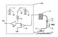
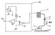
上記のワイヤボンディング工程においては、ワイヤ12とワーク14の間に電流を流すことによって、ワイヤの不着の検出を行っている。この電気的不着検出は図11、図12に示すような手段で行われる。図11は直流電流をワイヤとワークの間に流す直流式通電状態取得手段22aを示す図であり、図12は交流をワイヤと、ワークの間に流す交流式通電状態取得手段22bを示している。 In the above-described wire bonding process, the non-bonding of the wire is detected by passing a current between the
直流式通電状態取得手段22aは、ワイヤが半導体チップ2に接続されている場合に、ワイヤ12とワーク14の間に電流が流れることを利用してワイヤの接合、不着を検出するための通電状態を取得するもので、ワイヤ12に正の電圧を掛けるための正電圧電源55と、ワイヤ12に負の電圧を掛ける負電圧電源56とを備え、この二つの電源を切替える切替えスイッチ54によって正、負いずれかの電源が抵抗57を介して検出器58の入力側に接続されている。一方、検出器58の入力側には、ワイヤ12への電流を入切する入切スイッチ52が設けられ、入切スイッチ52はワイヤ12が巻回されているスプール11と接続されてワイヤ12と電気的に接続されている。直流式通電状態取得手段22aが正負、2種類の電源を備えているのは、半導体チップ2の回路の構成によって、パッド3には正の電流を流すものと負の電流を流すものがあるためである。 The DC-type energization
このように構成された直流式通電状態取得手段22aは、次のような動作によって通電状態を取得する。第1ボンド点の特性によって切替えスイッチ54によって正電圧又は負電圧の電源が選択される。入切スイッチ52が閉じられると、電源の一方はワーク14と共にアースされていることから、電流は電源55または56からパッド3を通して半導体のチップ2に流れる。このとき、ワイヤ12が不着である場合には、電流はワイヤ12には流れず、検出器58に向かって流れ、検出器58の出力端子59の電圧が上昇又は下降する(例えば、特許文献1、2参照)。この電圧の変化を捉えて不着の検出を行う。 The DC-type energization
一方、半導体チップ2の回路の特性上、いくつかのパッド3(第1ボンド点)は抵抗が非常に大きくワーク14と導通せず、直流電流がまったく流れない特性を持っている。このように直流電流が流れないパッド3(第1ボンド点)につては、上記の直流式通電状態検出手段22aでは通電状態の検出ができない。そこで、このような直流式通電状態取得手段22aが使えないパッド3(第1ボンド点)の通電状態を取得する手段として交流式通電状態取得手段22bがある。これは、ワイヤ12とワーク14の間に交流電流を流すもので、パッド3と半導体チップ2が持っている静電容量によって交流電流が流れることを利用したものである。動作は上記の直流式通電状態取得手段22aと同様で、入切スイッチ52を入れることによってワイヤ12に交流電流を流して通電状態を取得する。 On the other hand, due to the characteristics of the circuit of the
ところが、このような交流式通電状態取得手段22bは、パッド3と半導体チップ2が持っている静電容量が非常に小さい場合には、交流電流が流れず通電状態が検出できない。このような直流式、交流式の通電状態取得手段22a,22bは切り替えることが困難であることから、1つの半導体チップ2については、直流式か交流式のどちらか一方が使用される。このため1つの半導体チップ2には、通電状態取得手段によって通電状態が取得できず、電気的不着検出工程を適用して不着検出ができない特定ボンド点がある。このような特定ボンド点は、半導体チップ2の特性で決まるため、ボンディング前にどの点が特定ボンド点かはわかっており、特定ボンド点では通電の検出がなくともその点は不着ではなく、接合されているものとして処理されている。そして、製造終了後、ボンディングされたリードフレームを随時あるいは一定時間ごとに取り出して、別の顕微鏡などを使った検査工程で検査しているが、検査がオフラインで行われていることから検査の結果をすぐに製造装置の運転に反映できず、不良品が大量に発生してしまう問題があった(例えば、特許文献3参照)。 However, such an AC energization
このような問題に対して、製品をラインから取り出さずに光学的な不着検出工程によって不着の検出を行うことが提案されている(例えば、特許文献3,4参照)。これはボンディング部を撮像して、その画像データを分析することによって、不着検出を行うものである。この撮像手段視野60の画像の一例を図10(a)、(b)に示す。図10(a)は正常なボンディング部の画像を示し、図10(b)は不着状態示す。図10(b)の中央は圧着ボールがないボンディング点、下と上はボンディング位置がずれている場合を示している。このように、光学的不着検出工程は撮像データ上に第1ボンディング部6(圧着ボール)の有無あるいはその位置を検出することによって不着の検出を行うものである。 In order to solve such a problem, it has been proposed to detect non-sticking by an optical non-sticking detection process without taking out a product from the line (see, for example,
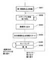
しかし、このような従来技術では、ボンディングの後リードフレームをワイヤボンディング装置から取り外さないで光学的な不着検出を行うものの、図9のフローチャートに示すように検査工程はボンディング工程とは別工程となっており、一端すべてのパッド3のボンディングが終了してから、すべてのパッド3の画像を順次取り込んで光学的な検査を行っていくものであった(例えば、特許文献3,4参照)。 However, in such a conventional technique, after the bonding, an optical non-bonding detection is performed without removing the lead frame from the wire bonding apparatus, but the inspection process is separate from the bonding process as shown in the flowchart of FIG. Then, after bonding of all the
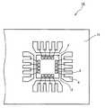
このような従来の光学的不着検査工程はすべてのボンディング部を光学的に検査していくことから検査工程に時間がかかるため、生産効率が落ちるという問題があった。また、近年の半導体チップ2の複雑化、高集積化によって増加してきている多重配線、スタック配線などの重ね配線には対応できないという問題があった。多重配線では図6に示すように、半導体チップ2上に複数列のパッド3、3’が配置され、これに対応して複数列のリード7、7’が配置されている。各々の半導体チップ2の端面に近いパッド3、リード7がワイヤ12で接続され、半導体チップ2の端面から遠い側のパッド3’、リード7’はワイヤ12’で接続されている。このワイヤ12’は図6に示すようにパッド3、リード7、ワイヤ12をまたぐようにパッド3’とリード7’を接続している。また、図7に示すようにスタック配線は半導体チップ2が複数段の階層構造になっており、階層ごとにパッド3が配置され、上記の多重配線と同様に各々の半導体チップ2の端面に近いパッド3、リード7がワイヤ12で接続され、半導体チップ2の端面から遠い側のパッド3’、リード7’はワイヤ12’で、パッド3、リード7がワイヤ12をまたぐように接続されている。このような多重配線、スタック配線のワイヤボンディングは最初に半導体チップ2の端面に近い側のワイヤ12のボンディングを行い、その後半導体チップ2の端面から遠い側のワイヤ12’のボンディングを行っている。そして、半導体チップ2の端面に近い側のパッド3、リード7、ワイヤ12の上を半導体チップ2の端面から遠い側のワイヤ12’がまたいでいることから、ボンディング終了後の撮像手段を用いた光学的不着検出では、半導体チップ2の端面から遠い側のワイヤ12’の下に隠れる半導体チップ2の端面に近い側のパッド3、リード7の撮像ができず、不着の検出が困難であるという問題があった。 Such a conventional optical non-bonding inspection process optically inspects all the bonding portions, and therefore requires a long time for the inspection process, resulting in a problem that production efficiency is lowered. In addition, there has been a problem that it is not possible to cope with overlapping wirings such as multiple wirings and stack wirings, which have been increasing due to the complexity and high integration of the
更に、従来技術では平面画像を処理して光学的な不着検出をしていることから、図8のように平面的には第1ボンディング部6がパッド3の上に重なって見えるものの、実際には第1ボンディング部6がパッド3から離れている状態の不着が検出できないという問題があった。 Furthermore, in the prior art, since the planar image is processed to detect optical non-stickiness, the
そこで本発明の目的は、電気的不着検出工程の適用できない特定ボンド点について、ボンディング工程中に撮像手段を用いた光学的不着検出工程による不着検出を行い、短時間に精度よく不着検出を行うことができるボンディング方法を提供することにある。また、本発明は、多重配線、スタック配線などの重ね配線のボンディングにおいても確実に光学的不着検出工程が適用できるようなボンディング方法を提供することにある。更に、ボンディング部がパッドから浮き上がっている状態の不着検出を確実に行うことができるようなボンディング方法を提供することにある。 Accordingly, an object of the present invention is to perform non-stick detection by an optical non-stick detection process using an imaging means during a bonding process for a specific bond point to which the electrical non-stick detection process is not applicable, and accurately detect non-stick in a short time. It is to provide a bonding method capable of achieving the above. It is another object of the present invention to provide a bonding method in which the optical non-sticking detection process can be reliably applied to bonding of overlapping wirings such as multiple wirings and stack wirings. Another object of the present invention is to provide a bonding method capable of reliably detecting non-bonding in a state where the bonding portion is lifted from the pad.
本発明のボンディング方法は、ワイヤが挿通されてワークにボンディングを行うキャピラリをXYZ方向に移動させる移動機構と、ワイヤとワークの間に通電し、その通電状態を検出する通電状態取得手段と、ワークを撮像する撮像手段と、ボンディング装置を制御するボンディング制御部と、データを記憶している記憶部と、を備え、第1ボンド点と第2ボンド点との間及び、該第1ボンド点または該第2ボンド点または該第1ボンド点と該第2ボンド点との間を接続するワイヤをまたいで、他の第1ボンド点と他の第2ボンド点との間をワイヤで接続する重ね配線に用いられるワイヤボンディング装置のボンディング方法であって、通電状態取得手段によって取得された第1ボンド点とワイヤとの間または他の第1ボンド点とワイヤとの間の通電状態信号を処理して第1ボンド点とワイヤとの間または他の第1ボンド点とワイヤとの間の不着を電気的に検出する電気的不着検出工程と、撮像手段によって取得された画像を処理して第1ボンド点とワイヤとの間または他の第1ボンド点とワイヤとの間の不着を光学的に検出する光学的不着検出工程と、それぞれの第1ボンド点または他の第1ボンド点が電気的不着検出工程を適用することができない特定ボンド点であるかどうかのデータを記憶部から取得するデータ取得工程と、データ取得工程によって取得されたデータによって第1ボンド点または他の第1ボンド点が特定ボンド点でないと判断された場合に、該第1ボンド点または該他の第1ボンド点にボンディングを行った都度、電気的不着検出工程によって不着確認を行い、データ取得工程によって取得されたデータによって第1ボンド点または他の第1ボンド点が特定ボンド点であると判断された場合に、該第1ボンド点または該他の第1ボンド点にボンディングを行った都度、光学的不着検出工程によって不着確認を行う不着確認工程と、を有することを特徴とする。Thebonding method of the present invention includes a moving mechanism that moves a capillary for bonding to a workpiece by insertinga wire in the XYZ directions, an energization state acquisition unit that energizes between the wire and the workpiece, and detects the energization state, imaging means for imaging and a bonding control unit for controlling the bonding apparatus, and a storage unit for storing data, between a first bonding point and a second bonding pointand the first bonding point or Overlap connecting the second bond point or the wire connecting between the first bond point and the second bond point and connecting the wire between the other first bond point and the other second bond point a bonding method of a wire bondingdevice used in the wiring,the first bonding point or betweenthe other and the first bonding point and the wire acquired by the electrical conduction state acquisition deviceand the wire and the Electrically non-bonding detection step for electrically detecting a non-bondingbetween or between other first bonding point and the wire between the first bonding point and the wire by processing the conductive state signal, acquired by the image pickup means an optical non-bonding detection step of detecting a non-bondingbetween or between other first bonding point and the wire between the first bonding pointand the wire by processing image optically, first bonding pointor other, respectively a data acquisition stepof first bonding point get the whether specific bonding point can not be applied to electrical non-bonding detection step data from the storage unit, first bonding point bythe data acquisition step thus obtained dataoriftheother first bonding pointis determined not to be a specific bondingpoint, each time performing the bonding in the first bonding point or said other first bonding point, line a non-delivery check by an electrical non-bonding detection step When the first bond point or the other first bond point is determined to be the specific bond point based on the data acquired by the data acquisition process, the first bond point or the other first bond point is bonded. And a non-sticking confirmation step of performing non-sticky confirmation byan optical non-sticky detection stepeach time it is performed.
また、光学的不着検出工程は、複数の撮像手段によって取得された複数の画像を処理して、第1ボンド点のワイヤの不着を光学的に検出する光学的不着検出工程であってもよい。Also, the light histological non-bonding detection step processes the plurality of images acquired by the plurality of imaging means, be an optical non-bonding detection step of detecting a non-bonding of the wire of the first bonding point optically Good.
本発明のボンディング制御プログラムは、ワイヤが挿通されてワークにボンディングを行うキャピラリをXYZ方向に移動させる移動機構と、ワイヤとワークの間に通電し、その通電状態を検出する通電状態取得手段と、ワークを撮像する撮像手段と、ボンディング装置を制御するボンディング制御部と、データを記憶している記憶部と、を備え、第1ボンド点と第2ボンド点との間及び、該第1ボンド点または該第2ボンド点または該第1ボンド点と該第2ボンド点との間を接続するワイヤをまたいで、他の第1ボンド点と他の第2ボンド点との間をワイヤで接続する重ね配線に用いられるワイヤボンディング装置のボンディング制御プログラムであって、通電状態取得手段によって取得された第1ボンド点とワイヤとの間または他の第1ボンド点とワイヤとの間の通電状態信号を処理して第1ボンド点とワイヤとの間または他の第1ボンド点とワイヤとの間の不着を電気的に検出する電気的不着検出プログラムと、撮像手段によって取得された画像を処理して第1ボンド点とワイヤとの間または他の第1ボンド点とワイヤとの間の不着を光学的に検出する光学的不着検出プログラムと、それぞれの第1ボンド点または他の第1ボンド点が電気的不着検出プログラムを適用することができない特定ボンド点であるかどうかのデータを記憶部から取得するデータ取得プログラムと、データ取得プログラムによって取得されたデータによって第1ボンド点または他の第1ボンド点が特定ボンド点でないと判断された場合に、該第1ボンド点または該他の第1ボンド点にボンディングを行った都度、電気的不着検出プログラムによって不着確認を行い、データ取得プログラムによって取得されたデータによって第1ボンド点または他の第1ボンド点が特定ボンド点であると判断された場合に、該第1ボンド点または該他の第1ボンド点にボンディングを行った都度、光学的不着検出プログラムによって不着確認を行う不着確認プログラムと、を有することを特徴とする。Thebonding control program of the present inventionincludes a moving mechanism that moves a capillary for bonding to a workpiece by insertinga wire in the XYZ directions, energization between the wire and the workpiece, and an energization state acquisition unit that detects the energization state, An image pickup unit for picking up an image of a workpiece, a bonding control unit for controlling a bonding apparatus, and a storage unit for storing data, and between the first bond point and the second bond point, and thefirst bond point Alternatively, the second bond point or a wire connecting between the first bond point and the second bond point is straddled and a wire is connected between another first bond point and another second bond point. a bonding control program for a wire bondingapparatus used for overlapping interconnection between a first bonding point and a wire obtained by the electrical conduction state acquisition meansor other first Electrically non-bonding detection program for electrically detecting a non-bondingbetween thecommand pointsorbetweenanother first bonding point and the wire between the first bonding point and the wire by processing the conductive state signalbetween the wire an optical non-bonding detection program for detecting a non-bonding optically inor between other first bonding point and the wire between the first bonding pointand the wire by processing the image acquired by the imaging means, respectively a data acquisition program first bonding pointor the other of the first bonding point get the whether specific bonding point can not be applied to electrical non-bonding detection program data from the storage unit, thus acquiredin the data acquisition program andwhen the first bonding pointor other first bonding point by the datais determined to be not specific bondingpoint, bonding the first bonding point or said other first bonding point Each time that Tsu performs non-delivery check by an electrical non-bonding detection program, whenthe first bonding point or other first bonding point by data acquired by the data acquisition program is determined tobe a specific bonding point,said And a non-sticking confirmation program for performing non-sticky confirmation byan optical non-sticky detection programeach time bonding is performed to one bond point or another first bond point.
また、光学的不着検出プログラムは、複数の撮像手段によって取得された複数の画像を処理して、第1ボンド点のワイヤの不着を光学的に検出する光学的不着検出プログラムであってもよい。Further, the light histological non-bonding detection program processes the plurality of images acquired by the plurality of imaging means, it may be an optical non-bonding detection program for detecting a non-bonding of the wire of the first bonding point optically .
本発明のワイヤボンディング装置は、ワイヤが挿通されてワークにボンディングを行うキャピラリをXYZ方向に移動させる移動機構と、ワイヤとワークの間に通電し、その通電状態を検出する通電状態取得手段と、ワークを撮像する撮像手段と、ボンディングを制御するボンディング制御部と、データを記憶している記憶部と、を備え、第1ボンド点と第2ボンド点との間及び、該第1ボンド点または該第2ボンド点または該第1ボンド点と該第2ボンド点との間を接続するワイヤをまたいで、他の第1ボンド点と他の第2ボンド点との間をワイヤで接続する重ね配線に用いられるワイヤボンディング装置であって、ボンディング制御部は、通電状態取得手段によって取得された第1ボンド点とワイヤとの間または他の第1ボンド点とワイヤとの間の通電状態信号を処理して第1ボンド点とワイヤとの間または他の第1ボンド点とワイヤとの間の不着を電気的に検出する電気的不着検出手段と、撮像手段によって取得された画像を処理して第1ボンド点とワイヤとの間または他の第1ボンド点とワイヤとの間の不着を光学的に検出する光学的不着検出手段と、それぞれの第1ボンド点または他の第1ボンド点が電気的不着検出手段を適用することができない特定ボンド点であるかどうかのデータを記憶部から取得するデータ取得手段と、データ取得手段によって取得されたデータによって第1ボンド点が特定ボンド点でないと判断された場合に、該第1ボンド点または該他の第1ボンド点にボンディングを行った都度、電気的不着検出手段によって不着確認を行い、データ取得プログラムによって取得されたデータによって第1ボンド点または他の第1ボンド点が特定ボンド点であると判断された場合に、該第1ボンド点または該他の第1ボンド点にボンディングを行った都度、光学的不着検出手段によって不着確認を行う不着確認手段と、を有することを特徴とする。Thewire bonding apparatus of the present invention includes a moving mechanism that moves a capillary for bonding to a workpiece by insertinga wire in the XYZ directions, an energization state acquisition unit that energizes between the wire and the workpiece, and detects the energization state. An image pickup means for picking up an image of a workpiece;a bonding control unitfor controlling bonding; and a storage unit for storing data;and between the first bond point and the second bond point, Overlap connecting the second bond point or the wire connecting between the first bond point and the second bond point and connecting the wire between the other first bond point and the other second bond point a wire bonding apparatus thatis used in the wiring, bonding control unit,or betweenother first bonding point and the wire between the first bonding point and the wire acquired by the electrical conduction state acquisition device Electrically non-bonding detection means for electrically detecting the non-bondingbetween or between other first bonding point and the wire of the process the conduction state signal first bonding point and the wirebetween, by the imaging means optical non-bonding detection means and, respectively, a first bonding point of the optically detectable non-bondingbetween or between other first bonding point and the wire between the first bonding pointand the wire by processing the acquired imageor a data acquisition meansfor the other first bonding point get the whether specific bonding point can not be applied to electrical non-bonding detection means data from the storage unit, first bythe thus acquired data data acquisition meanswhen one bonding pointis determined not to be a specific bondingpoint, each time performing the bonding in the first bonding point or said other of the first bonding point, performs non-delivery confirmation by the electrical non-bonding detection means, data acquiring flopWhenthefirst bonding point or other first bonding point by data obtained by gram is determined tobe a specific bondingpoint,each time performing the bonding in the first bonding point or said other first bonding point And non-sticking confirmation means for performing non-sticking confirmation by the optical non-sticking detection means.
また、光学的不着検出手段は、複数の撮像手段によって取得された複数の画像を処理して、第1ボンド点のワイヤの不着を光学的に検出する光学的不着検出手段であっても良い。Further, the light histological non-bonding detection means processes the plurality of images acquired by the plurality of imaging means, may be an optical non-bonding detection means for detecting a non-bonding of the wire of the first bonding point optically .
本発明は、電気的不着検出工程を適用できない特定ボンド点について、ボンディング工程中に撮像手段を用いた光学的不着検出工程による不着検出を行い、短時間に精度よく不着検出を行うことができるという効果を奏する。 According to the present invention, it is possible to perform non-stick detection by an optical non-stick detection process using an imaging means during a bonding process for a specific bond point to which the electrical non-stick detection process cannot be applied, and to accurately detect non-stick in a short time. There is an effect.
以下、本発明の実施形態について説明する。説明において、従来技術と同様の部分には同様の符号を付して説明は省略する。 Hereinafter, embodiments of the present invention will be described. In the description, the same parts as those in the prior art are denoted by the same reference numerals, and the description thereof is omitted.
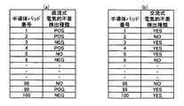
本発明によるワイヤボンディング装置10は、図1に示すように、XYテーブル20の上にボンディングヘッド19が設置され、ボンディングヘッド19にモータにてZ方向に移動されるボンディングアーム13を備え、ボンディングアーム13の先端にキャピラリ16が取り付けられている。XYテーブル20とボンディングヘッド19は移動機構18を構成し、移動機構18はXYテーブル20によってボンディングヘッド19を水平面内(XY面内)で自在な位置に移動することができ、これに取り付けられたボンディングアーム13をZ方向に移動させることによって、ボンディングアーム13先端のキャピラリ16をXYZの方向に自在に移動させることができる。ボンディングアーム13の先端にはワイヤ12が挿通されており、ワイヤ12はスプール11に巻回されている。スプール11に巻回されたワイヤ12にはワイヤ12とワーク14の間の通電状態を取得する通電状態取得手段22が接続されている。ボンディングヘッド19にはキャピラリ16と共にZ方向に移動してワイヤ12を固定するクランパ17が開閉自在に取り付けられている。また、ボンディングヘッド19には、半導体チップ2の位置及びワークの撮像を行う撮像手段28が取り付けられている。また、ワイヤ12の先端付近にはワイヤ12との間で放電を行ってワイヤ12先端をボール5に形成するためのボール形成手段26(電気トーチ)が取り付けられている。撮像手段28は撮像手段インターフェース40に接続され、通電状態取得手段22は通電状態取得手段インターフェース42に接続され、移動機構18は移動機構インターフェース44に接続されている。そして各インターフェースはデータバス32を介してワイヤボンディング装置の制御を行う制御部30に接続されている。また、データバス32には制御用のデータ及び図3に示す各パッド3(第1ボンド点)の電気的不着検出種類表のデータを格納している記憶部34が接続されている。 As shown in FIG. 1, a wire bonding apparatus 10 according to the present invention is provided with a
電気的不着検出種類表は、各パッドにおいてどのような電気的不着検出が可能かを記録したデータテーブルであって、ある半導体チップ2の不着検出に直流式通電状態取得手段22aが用いられる時に、各パッドが正電圧電源55を使う点であるのか(図3(a)でPOSとして示す)、負電圧電源56を使う点であるのか(図3(a)でNEGとして示す)、抵抗が非常に大きく直流式通電状態取得手段22aでは通電状態の取得ができない点(図3(a)でNOとして示す)であるのかのデータを有している。また、半導体チップ2の不着検出に交流式通電状態取得手段が用いられる時に、各パッドが交流式通電状態取得手段22bを用いることができる点であるか(図3(b)でYESとして示す)、静電容量が非常に小さく交流式通電状態取得手段22bでは通電状態の取得ができない点(図3(b)でNOとして示す)であるのかのデータを有している。 The electrical non-detection type table is a data table recording what kind of non-electricity detection is possible in each pad, and when the DC energization state acquisition means 22a is used for non-detection of a
このように構成されるワイヤボンディング装置10は制御部30によって制御され、次のような工程によってワイヤボンディングと不着検出を行う。以下の説明は直流式通電状態取得手段22aが使用される半導体チップ2にボンディングを行う工程について説明する。以下の説明では、まず、参考例として多重配線ではない場合のボンディング工程について説明する。
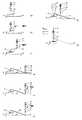
(1)ボール形成手段26(電気トーチ)によってワイヤ12先端をボール5に形成し、撮像装置28によって半導体チップ2の位置検出し、移動機構18によりキャピラリ16をN番目のパッド3(第1ボンド点)の上に移動させる(図2、ステップ103、図4(a))。
(2)制御部30は記憶部34の電気的不着検出種類表のから、該当するパッド点の直流式電気的不着検出種類データを取得する(図2、ステップS104)。例えばN=1の場合には、正電圧電源55を使用する点を表す「POS」のデータを取得し、N=3の場合には負電圧電源56を使用する点を表す「NEG」のデータを取得し、N=5の場合には直流式通電状態取得手段22aでは通電状態を取得できない点を表す「NO」のデータを取得する。
(3)制御部30は取得したデータによって、当該N番目のパッド3(第1ボンド点)が電気的不着検出工程を適用することができない特定ボンド点かどうかを判断する(図2、ステップS105)。上記の例ではN=5のパッド(第1ボンド点)は特定ボンド点と判断され、N=1,3は通常のボンド点と判断される。
(4)当該ボンド点がN=1,3のような通常ボンド点の場合には、取得した直流式電気的不着検出種類が「POS」であれば、図11の切替えスイッチ54を正電圧電源55の側に切替え、取得した直流式電気的不着検出種類が「NEG」であれば、図11の切替えスイッチ54を負電圧電源56の側に切替える(図2、ステップS106)。
(5)キャピラリ16を下動させて、パッド3(第1ボンド点)上にボンディングを行う(図2、ステップS107、図4(b))。パッド3(第1ボンド点)上にはボール5が圧着して第1ボンディング部6(圧着ボール)が形成される。
(6)ボールが圧着された状態で、直流式通電状態取得手段22aの入切スイッチ52が閉じられて、電流がワイヤ12とワーク14の間に流れ、このときの電圧が基準電圧として直流式通電状態取得手段22aに取得される。取得されたデータは通電状態取得手段インターフェース42を介して制御部30に入力される(図2、ステップS108、図4(b))。
(7)移動機構18は、パッド3(第1ボンド点)からキャピラリ16を上昇させ、次いでキャピラリ16を横に移動させる(図2、ステップS109、図4(c))。
(8)キャピラリ16の移動中に、直流式通電状態取得手段22aの入切スイッチ52が閉じられて、電流がワイヤ12とワーク14の間に流れ、このときの通電状態が直流式通電状態取得手段22aに取得される。取得されたデータは通電状態取得手段インターフェース42を介して制御部30に入力される(図2、ステップS110、図4(c))。
(9)直流式通電状態取得手段22aの信号を制御部30で電気的不着検出手段によって処理することによりパッド3(第1ボンド点)の不着が検出される。たとえば、ステップS108で取得された基準電圧とステップS110にて取得された通電状態の電圧に差があれば不着と判断し、電圧が同等であれば不着なしと判断する。不着が検出された場合でも、キャピラリ16はそのままリード4(第2ボンド点)に移動を続け、リード4(第2ボンド点)にボンディングを行った後エラーにて停止する(図2、ステップS115からS116)。ただし、リード4(第2ボンド点)におけるノーテール状態、リード不着状態を検出するための通電状態の取得は行わない。
(10)電気的不着検出手段によって不着が検出されず、正常に接合されたと判断された場合には、キャピラリ16はそのままリード4(第2ボンド点)に移動を続け、リード4(第2ボンド点)にボンディングを行った後、リード4(第2ボンド点)におけるノーテール状態、リード不着状態を検出するための通電状態取得を行いリード(第2ボンド点)の不着検出を行う(図2、ステップS112)。The wire bonding apparatus 10 configured as described above is controlled by the
(1) The tip of the
(2) The
(3) Based on the acquired data, the
(4) When the bond point is a normal bond point such as N = 1, 3, if the acquired DC type electric non-detection type is “POS”, the changeover switch 54 of FIG. If the acquired DC type electrical non-detection type is “NEG”, the selector switch 54 in FIG. 11 is switched to the negative
(5) The capillary 16 is moved downward to perform bonding on the pad 3 (first bond point) (FIG. 2, step S107, FIG. 4B). On the pad 3 (first bond point), the
(6) With the ball pressed, the on / off
(7) The moving
(8) While the capillary 16 is moving, the on / off
(9) The non-attachment of the pad 3 (first bond point) is detected by processing the signal of the DC-type energization state acquisition means 22a by the electrical non-stick detection means in the
(10) If it is determined that the non-bonding is not detected by the electric non-bonding detecting means and the bonding is normally performed, the capillary 16 continues to move to the lead 4 (second bond point), and the lead 4 (second bond) After bonding to a point), an energization state is acquired to detect a no-tail state and a lead non-bonding state in the lead 4 (second bonding point), and non-sticking detection of the lead (second bonding point) is performed (FIG. 2, Step S112).
(11)図2、ステップS105において、当該ボンド点がN=5のような電気的不着検出工程が適用できない特定ボンド点であると判断された場合には、制御部30は直流式電気的通電状態取得手段22aを動作させず、キャピラリ16を下動させて、パッド3(第1ボンド点)上にボンディングを行う(図2、ステップS117、図4(b))。パッド3(第1ボンド点)上にはボール5が圧着して第1ボンディング部6(圧着ボール)が形成される。
(12)その後、通常のボンド点と同様にキャピラリを上昇させて、リード4(第2ボンド点)へのボンディング、ノーテール検出、リード不着検出を行う(図2、ステップS119、図4(c)から(f))。
(13)制御部30は移動機構18によってCCDカメラなどで構成される撮像手段28をパッド3(第1ボンド点)がその視野60に入る位置に移動させる(図2、ステップS120)。そして、特定ボンド点てあるパッド3(第1ボンド点)の周りの平面画像を取得する(図2、ステップS121、図4(g))。取得された平面画像は従来技術で述べたのと同様、撮像手段インターフェース40を介して制御部30に入力され、その画像が分析される(図2、ステップS122)。取得された平面画像はたとえば図10に示すようになっている。図10(a)は正常にボンディングができている状態を示し、図10(b)は不着状態を示す。
(14)光学的不着検出工程によって特定ボンド点のパッド3(第1ボンド点)が不着であると判断された場合には、エラー処理を行い、ワイヤボンディング装置10は停止する(図2、ステップS116)。
(15)不着が検出されず、正常に接合されたと判断された場合には、次のパッド3(第1ボンド点)に移動してボンディング続けていく(図2、ステップS113、S114、図4(h))。
(16)すべての点のボンディング、検査が終了すると、ボンディング動作は終了する(図2、ステップS123)。(11) If it is determined in FIG. 2 and step S105 that the bond point is a specific bond point to which the electrical non-stick detection process such as N = 5 cannot be applied, the
(12) Thereafter, the capillary is raised in the same manner as a normal bond point, and bonding to the lead 4 (second bond point), no tail detection, and lead non-stick detection are performed (FIG. 2, step S119, FIG. 4C). To (f)).
(13) The
(14) If it is determined by the optical non-bonding detection step that the pad 3 (first bond point) at the specific bond point is non-bonded, error processing is performed and the wire bonding apparatus 10 stops (FIG. 2, step). S116).
(15) When non-bonding is not detected and it is determined that the bonding is normally performed, the bonding is continued by moving to the next pad 3 (first bonding point) (FIG. 2, steps S113, S114, FIG. 4). (H)).
(16) When bonding and inspection of all points are completed, the bonding operation is completed (FIG. 2, step S123).
以上、直流式の通電状態取得手段22aを用いて通電状態を取得して、電気的不着検出を行うボンディング方法について説明したが、交流を用いる場合も全体の基本工程は同様である。ただし、交流式の場合には、交流電源51を使用するので、正電圧電源55と負電圧電源56とを切り替える必要が無いことから、図2、ステップS106の不着検出回路の切替えは行わない。 As described above, the bonding method of acquiring the energized state using the DC-type energized
以上述べたように、本参考例は、電気的不着検出工程の適用できない特定ボンド点について、ボンディング工程中に撮像手段を用いた光学的不着検出工程による不着検出を行い、短時間に精度よく不着検出を行うことができ、生産効率の向上を図ることが出来ると共に、製造プロセスの中で、オンライン上で特定ボンド点の不着検出が出来ることから不着の発生した時点でその不着を確実に検出することができ、不良品の低減、品質向上を図ることができるという効果を奏する。As described above, thisreference example performs non-stick detection in the optical non-stick detection process using an imaging means during the bonding process for a specific bond point to which the electrical non-stick detection process is not applicable, so that the non-stick is accurately performed in a short time. It is possible to detect and improve production efficiency, and it is possible to detect non-bonding of a specific bond point online in the manufacturing process, so that non-bonding is reliably detected when non-bonding occurs. It is possible to reduce defective products and improve quality.
次に、図6に示す多重配線の特定ボンド点をボンディングする場合の工程について説明する。通常配線のボンディング工程と同様部分には同様の符号を付して説明は省略する。
(1)半導体チップ2の端面に近い側のパッド3が特定ボンド点のとき、半導体チップ2の端面に近い側のパッド3、リード7との間をワイヤ12で接続した後、特定ボンド点であるパッド3(第1ボンド点)の上に撮像装置28を移動させて光学的不着検出工程によって、その不着検出を行う(図5(a))。
(2)ボール形成手段26(電気トーチ)によってワイヤ12先端をボール5に形成し、撮像装置28によって半導体チップ2の位置を検出し、移動機構18によりキャピラリ16を半導体チップ2の端面から遠い側のパッド3’(第1ボンド点)の上に移動させる(図5(b))。
(3)通常配線のボンディングと同様の工程によって、半導体チップ2の端面から遠い側のパッド3’とリード7’との間をワイヤ12’によって接続する。このワイヤ12’は図5(c)、図5(d)、図6に示すようにパッド3、リード7、ワイヤ12をまたいで接続される。
(4)リード4(第2ボンド点)へのボンディングが終了したら、移動機構18によりキャピラリ16を、特定ボンド点である半導体チップ2の端面から遠い側のパッド3’(第1ボンド点)の上に移動させ、撮像装置28によって光学的に特定ボンド点であるパッド3’の不着検出を行う。
(5)パッド3、3’が特定ボンド点でない場合には、通常のボンディング工程と同様に直流式通電状態取得手段22aによって通電状態を取得して、電気的不着検出工程によって不着の検出、判断を行う。Next, a process for bonding a specific bond point of the multiple wiring shown in FIG. 6 will be described. Portions similar to those in the normal wiring bonding step are denoted by the same reference numerals, and description thereof is omitted.
(1) When the
(2) The tip of the
(3) A
(4) When bonding to the lead 4 (second bond point) is completed, the capillary 16 is moved by the moving
(5) When the
このように、本実施形態のボンディング方法では、ボンディングサイクルごとに、電気的不着検出工程の適用できない特定ボンド点を光学的不着検出手段によって不着検出しているので、多重配線のボンディングにおいても撮像視野をワイヤによって妨げられることなく確実に不着検出をすることが出来るという効果を奏する。一般に、このような多重配線や、スタック配線が用いられるのは集積度が高くパッド数が多い半導体チップであることから、このような精度の高い不着検出方法はより効果的に不良品を低減することができ、大きく生産効率を向上させることが出来るという効果を奏する。 As described above, in the bonding method of the present embodiment, the specific bonding point to which the electrical non-detection process cannot be applied is detected by the optical non-bonding detecting means for each bonding cycle, so that the imaging field of view can be obtained even in the bonding of multiple wirings. It is possible to reliably detect non-bonding without being obstructed by the wire. In general, such a multiple wiring or stack wiring is used for a semiconductor chip having a high degree of integration and a large number of pads. Therefore, such a highly accurate non-sticking detection method more effectively reduces defective products. Can be produced, and the production efficiency can be greatly improved.
本実施形態のボンディング工程では、平面画像を取得する撮像手段28は制御部30の指令によって、その位置を自在に移動させることが出来るので、1つのパッド3(第1ボンド点)あるいは第1ボンディング部6の平面画像を異なる2点からの撮像することが出来る(図8)。このように2点からの撮像画像を処理することによって、パッド3(第1ボンド点)と第1ボンディング部6の高さの差を測定することが出来る。そしてこの高さの差が所定の閾値以上である場合には、第1ボンディング部6はパッド3から浮き上がっていると判断して、不着検出することが出来る。 In the bonding process of the present embodiment, the imaging means 28 for acquiring a planar image can move its position freely in accordance with a command from the
このように、本実施形態は、平面画像のみでなく異なる2点からの撮像データを処理することにより、高さ方向の距離を測定し、より正確に光学的に不着検出をすることが出来るという効果を奏する。 As described above, according to the present embodiment, it is possible to measure the distance in the height direction by processing not only the planar image but also the imaging data from two different points, and more accurately optical non-stick detection. There is an effect.
2 半導体チップ、3 第1ボンド点(パッド)、4 第2ボンド点(リード)、5 ボール、6 第1ボンディング部(圧着ボール)、7 第2ボンディング部、8 テールワイヤ、10 ワイヤボンディング装置、11 スプール、12 ワイヤ、13 ボンディングアーム、14 ワーク、15 リードフレーム、16 キャピラリ、17 クランパ、18 移動機構、19 ボンディングヘッド、20 XYテーブル、22 通電状態取得手段、22a 直流式通電状態取得手段、22b 交流式通電状態取得手段、23 基板、26 ボール形成手段(電気トーチ)、28 撮像手段、30 制御部(CPU)、32 データバス、34 記憶部(メモリ)、40 撮像手段インターフェース、42 通電状態取得手段インターフェース、44 移動機構インターフェース、51 交流電源、52 入切スイッチ、54 切替えスイッチ、55 正電圧電源、56 負電圧電源、57 抵抗、58 検出器、59 出力端子。 2 semiconductor chip, 3 first bond point (pad), 4 second bond point (lead), 5 ball, 6 first bonding part (crimp ball), 7 second bonding part, 8 tail wire, 10 wire bonding apparatus, 11 Spool, 12 Wire, 13 Bonding Arm, 14 Workpiece, 15 Lead Frame, 16 Capillary, 17 Clamper, 18 Movement Mechanism, 19 Bonding Head, 20 XY Table, 22 Energization State Acquisition Unit, 22a DC Type Energization State Acquisition Unit, 22b AC-type energization state acquisition means, 23 substrate, 26 ball formation means (electric torch), 28 imaging means, 30 control unit (CPU), 32 data bus, 34 storage unit (memory), 40 imaging means interface, 42 energization state acquisition Means interface, 44 moving mechanism Centers face, 51 AC power supply, 52 on-off switch, 54 switch, 55 a positive voltage supply, 56 the negative voltage power supply, 57 resistors, 58 a detector, 59 an output terminal.
Claims (6)
Translated fromJapaneseワイヤとワークの間に通電し、その通電状態を検出する通電状態取得手段と、
ワークを撮像する撮像手段と、
ボンディング装置を制御するボンディング制御部と、
データを記憶している記憶部と、
を備え、第1ボンド点と第2ボンド点との間及び、該第1ボンド点または該第2ボンド点または該第1ボンド点と該第2ボンド点との間を接続するワイヤをまたいで、他の第1ボンド点と他の第2ボンド点との間をワイヤで接続する重ね配線に用いられるワイヤボンディング装置のボンディング方法であって、
通電状態取得手段によって取得された第1ボンド点とワイヤとの間または他の第1ボンド点とワイヤとの間の通電状態信号を処理して第1ボンド点とワイヤとの間または他の第1ボンド点とワイヤとの間の不着を電気的に検出する電気的不着検出工程と、
撮像手段によって取得された画像を処理して第1ボンド点とワイヤとの間または他の第1ボンド点とワイヤとの間の不着を光学的に検出する光学的不着検出工程と、
それぞれの第1ボンド点または他の第1ボンド点が電気的不着検出工程を適用することができない特定ボンド点であるかどうかのデータを記憶部から取得するデータ取得工程と、
データ取得工程によって取得されたデータによって第1ボンド点または他の第1ボンド点が特定ボンド点でないと判断された場合に、該第1ボンド点または該他の第1ボンド点にボンディングを行った都度、電気的不着検出工程によって不着確認を行い、
データ取得工程によって取得されたデータによって第1ボンド点または他の第1ボンド点が特定ボンド点であると判断された場合に、該第1ボンド点または該他の第1ボンド点にボンディングを行った都度、光学的不着検出工程によって不着確認を行う不着確認工程と、
を有することを特徴とするボンディング方法。A moving mechanism that moves a capillary through which the wire is inserted and performs bonding to the workpiece in the XYZ directions;
Energization state acquisition means for energizing between the wire and the workpiece and detecting the energization state;
Imaging means for imaging a workpiece;
A bonding controller for controlling the bonding apparatus;
A storage unit storing data; and
Straddling a wire connecting between the first bond point and the second bond point and betweenthe first bond point or the second bond point or between the first bond point and the second bond point. A bonding method of a wire bonding apparatusused for an overlap wiring that connects a wire between another first bond point and another second bond point ,
The energization state signalbetween the first bond point and the wire or the other first bond point and the wire acquired by the energization state acquiring means is processed to process the first bond point and the wireor between the first bond point and the wire. An electrical non-bonding detecting step for electrically detecting non-bonding between one bond point and the wire ;
An optical non-bonding detection step of optically detecting the non-delivery ofor between other first bonding point and the wire between the first bonding pointand the wire by processing the image acquired by the imaging means,
A data acquisition step of acquiring data on whether or not each first bond pointor other first bond point is a specific bond point to which the electrical non-bonding detection step cannot be applied;
When the first bonding pointor other first bonding pointin the data acquisition step Hence the acquired datais judged not to be a specific bondingpoint, bonding the first bonding point or said other first bonding point Each time it is done, the non-stick check is performed by the electric non-stick detection process,
When the first bond point or the other first bond point is determined to be the specific bond point based on the data acquired by the data acquisition process, bonding is performed to the first bond point or the other first bond point. A non-sticking confirmation process for performing non-sticking confirmation byan optical non-sticky detection process,
A bonding method characterized by comprising:
を特徴とする請求項1に記載のボンディング方法。The optical non-sticking detection step is an optical non-sticking detection step of processing a plurality of images acquired by a plurality of imaging means to optically detect non-sticking of the wire at the first bond point. Item 2. A bonding method according to Item 1.
ワイヤとワークの間に通電し、その通電状態を検出する通電状態取得手段と、
ワークを撮像する撮像手段と、
ボンディング装置を制御するボンディング制御部と、
データを記憶している記憶部と、
を備え、第1ボンド点と第2ボンド点との間及び、該第1ボンド点または該第2ボンド点または該第1ボンド点と該第2ボンド点との間を接続するワイヤをまたいで、他の第1ボンド点と他の第2ボンド点との間をワイヤで接続する重ね配線に用いられるワイヤボンディング装置のボンディング制御プログラムであって、
通電状態取得手段によって取得された第1ボンド点とワイヤとの間または他の第1ボンド点とワイヤとの間の通電状態信号を処理して第1ボンド点とワイヤとの間または他の第1ボンド点とワイヤとの間の不着を電気的に検出する電気的不着検出プログラムと、
撮像手段によって取得された画像を処理して第1ボンド点とワイヤとの間または他の第1ボンド点とワイヤとの間の不着を光学的に検出する光学的不着検出プログラムと、
それぞれの第1ボンド点または他の第1ボンド点が電気的不着検出プログラムを適用することができない特定ボンド点であるかどうかのデータを記憶部から取得するデータ取得プログラムと、
データ取得プログラムによって取得されたデータによって第1ボンド点または他の第1ボンド点が特定ボンド点でないと判断された場合に、該第1ボンド点または該他の第1ボンド点にボンディングを行った都度、電気的不着検出プログラムによって不着確認を行い、
データ取得プログラムによって取得されたデータによって第1ボンド点または他の第1ボンド点が特定ボンド点であると判断された場合に、該第1ボンド点または該他の第1ボンド点にボンディングを行った都度、光学的不着検出プログラムによって不着確認を行う不着確認プログラムと、
を有することを特徴とするボンディング制御プログラム。A moving mechanism that moves a capillary through which the wire is inserted and performs bonding to the workpiece in the XYZ directions;
Energization state acquisition means for energizing between the wire and the workpiece and detecting the energization state;
Imaging means for imaging a workpiece;
A bonding controller for controlling the bonding apparatus;
A storage unit storing data; and
Straddling a wire connecting between the first bond point and the second bond point and betweenthe first bond point or the second bond point or between the first bond point and the second bond point. , A bonding control programfor a wire bonding apparatusused for overlapping wiring that connects a wire between another first bond point and another second bond point ,
The energization state signalbetween the first bond point and the wire or the other first bond point and the wire acquired by the energization state acquiring means is processed to process the first bond point and the wireor between the first bond point and the wire. An electrical non-bonding detection program for electrically detecting non-bonding between one bond point and a wire ;
An optical non-bonding detection program for detecting optically non-bondingbetween or between other first bonding point and the wire between the first bonding pointand the wire by processing the image acquired by the imaging means,
A data acquisition program for acquiring, from the storage unit, data as to whether or not each first bond pointor another first bond point is a specific bond point to which the electrical non-bonding detection program cannot be applied;
When the first bonding pointor other first bonding point bythe result acquired data data acquisition programis determined to be not specific bondingpoint, bonding the first bonding point or said other first bonding point Each time it is done, the non-stick check is performed by the electrical non-stick detection program,
When the data acquired by the data acquisition program determines thatthe first bond point or another first bond point is a specific bond point,bonding is performed to the first bond point or the other first bond point. A non-delivery confirmation program that performs non-delivery confirmation using an optical non-delivery detection program,
A bonding control program comprising:
を特徴とする請求項3に記載のボンディング制御プログラム。The optical non-stick detection program is an optical non-stick detection program for processing a plurality of images acquired by a plurality of imaging means and optically detecting non-stick of the wire at the first bond point. Item 4. A bonding control program according to item3 .
ワイヤとワークの間に通電し、その通電状態を検出する通電状態取得手段と、
ワークを撮像する撮像手段と、
ボンディングを制御するボンディング制御部と、
データを記憶している記憶部と、を備え、第1ボンド点と第2ボンド点との間及び、該第1ボンド点または該第2ボンド点または該第1ボンド点と該第2ボンド点との間を接続するワイヤをまたいで、他の第1ボンド点と他の第2ボンド点との間をワイヤで接続する重ね配線に用いられるワイヤボンディング装置であって、
ボンディング制御部は、
通電状態取得手段によって取得された第1ボンド点とワイヤとの間または他の第1ボンド点とワイヤとの間の通電状態信号を処理して第1ボンド点とワイヤとの間または他の第1ボンド点とワイヤとの間の不着を電気的に検出する電気的不着検出手段と、
撮像手段によって取得された画像を処理して第1ボンド点とワイヤとの間または他の第1ボンド点とワイヤとの間の不着を光学的に検出する光学的不着検出手段と、
それぞれの第1ボンド点または他の第1ボンド点が電気的不着検出手段を適用することができない特定ボンド点であるかどうかのデータを記憶部から取得するデータ取得手段と、
データ取得手段によって取得されたデータによって第1ボンド点が特定ボンド点でないと判断された場合に、該第1ボンド点または該他の第1ボンド点にボンディングを行った都度、電気的不着検出手段によって不着確認を行い、
データ取得プログラムによって取得されたデータによって第1ボンド点または他の第1ボンド点が特定ボンド点であると判断された場合に、該第1ボンド点または該他の第1ボンド点にボンディングを行った都度、光学的不着検出手段によって不着確認を行う不着確認手段と、
を有することを特徴とするワイヤボンディング装置。A moving mechanism that moves a capillary through which the wire is inserted and performs bonding to the workpiece in the XYZ directions;
Energization state acquisition means for energizing between the wire and the workpiece and detecting the energization state;
Imaging means for imaging a workpiece;
A bonding control unitfor controlling bonding;
A storage unit that stores data,and between the first bond point and the second bond point, and between the first bond point, the second bond point, or the first bond point and the second bond point. across wires connecting between, a wire bonding apparatus thatis used in the superposed wiring connecting wire between the other first bonding point between the other second bonding point,
The bonding controller
The energization state signalbetween the first bond point and the wire or the other first bond point and the wire acquired by the energization state acquiring means is processed to process the first bond point and the wireor between the first bond point and the wire. Electrical non-bonding detecting means for electrically detecting non-bonding between one bond point and a wire ;
An optical non-bonding detection means for detecting a non-delivery opticallyor between other first bonding point and the wire between the first bonding pointand the wire by processing the image acquired by the imaging means,
Data acquisition means for acquiring data on whether or not each first bond pointor another first bond point is a specific bond point to which the electrical non-bonding detection means cannot be applied, from the storage unit;
When the first bonding point bythe result acquired data data acquisition meansis determined to be not specific bondingpoint, each time performing the bonding in the first bonding point or said other of the first bonding point, electrical non-bonding Confirm non-delivery by the detection means
When the data acquired by the data acquisition program determines thatthe first bond point or another first bond point is a specific bond point,bonding is performed to the first bond point or the other first bond point. and each time a non-delivery confirmation means for performing a non-delivery check by optical non-bonding detection means,
A wire bonding apparatus comprising:
を特徴とする請求項5に記載のワイヤボンディング装置。The optical non-stick detection means is an optical non-stick detection means for processing a plurality of images acquired by a plurality of image pickup means to optically detect non-stick of the wire at the first bond point. Item 6. A wire bonding apparatus according to Item5 .
Priority Applications (4)
| Application Number | Priority Date | Filing Date | Title |
|---|---|---|---|
| JP2005378451AJP4547330B2 (en) | 2005-12-28 | 2005-12-28 | Wire bonding apparatus, bonding control program, and bonding method |
| TW095137271ATW200725767A (en) | 2005-12-28 | 2006-10-11 | Wire bonding apparatus, recording media with connecting control program and the connecting method |
| KR1020060104771AKR100841263B1 (en) | 2005-12-28 | 2006-10-27 | Wire bonding device, bonding control program and bonding method |
| US11/646,677US7699209B2 (en) | 2005-12-28 | 2006-12-28 | Wire bonding apparatus, record medium storing bonding control program, and bonding method |
Applications Claiming Priority (1)
| Application Number | Priority Date | Filing Date | Title |
|---|---|---|---|
| JP2005378451AJP4547330B2 (en) | 2005-12-28 | 2005-12-28 | Wire bonding apparatus, bonding control program, and bonding method |
Publications (2)
| Publication Number | Publication Date |
|---|---|
| JP2007180349A JP2007180349A (en) | 2007-07-12 |
| JP4547330B2true JP4547330B2 (en) | 2010-09-22 |
Family
ID=38305233
Family Applications (1)
| Application Number | Title | Priority Date | Filing Date |
|---|---|---|---|
| JP2005378451AExpired - Fee RelatedJP4547330B2 (en) | 2005-12-28 | 2005-12-28 | Wire bonding apparatus, bonding control program, and bonding method |
Country Status (4)
| Country | Link |
|---|---|
| US (1) | US7699209B2 (en) |
| JP (1) | JP4547330B2 (en) |
| KR (1) | KR100841263B1 (en) |
| TW (1) | TW200725767A (en) |
Families Citing this family (17)
| Publication number | Priority date | Publication date | Assignee | Title |
|---|---|---|---|---|
| JP4530984B2 (en)* | 2005-12-28 | 2010-08-25 | 株式会社新川 | Wire bonding apparatus, bonding control program, and bonding method |
| US7896218B2 (en)* | 2007-06-28 | 2011-03-01 | Western Digital Technologies, Inc. | Apparatus and method for conductive metal ball bonding with electrostatic discharge detection |
| JP4343985B2 (en)* | 2008-01-24 | 2009-10-14 | 株式会社新川 | Bonding apparatus and bonding stage height adjusting method for bonding apparatus |
| JP2010056106A (en)* | 2008-08-26 | 2010-03-11 | Nec Electronics Corp | Wire bonding device and wire bonding method using same |
| US8096462B2 (en)* | 2009-04-30 | 2012-01-17 | International Business Machines Corporation | Method of reworking electrical short in ultra sonic bonder |
| US20120074206A1 (en)* | 2010-09-27 | 2012-03-29 | Kulicke And Soffa Industries, Inc. | Methods of forming wire bonds for wire loops and conductive bumps |
| US9217759B2 (en)* | 2011-12-23 | 2015-12-22 | Sendyne Corporation | Current shunt |
| US9314869B2 (en)* | 2012-01-13 | 2016-04-19 | Asm Technology Singapore Pte. Ltd. | Method of recovering a bonding apparatus from a bonding failure |
| US20140076956A1 (en)* | 2012-09-20 | 2014-03-20 | Tyco Electronics Corporation | Soldering machine and method of soldering |
| SG11201503764YA (en) | 2012-11-16 | 2015-06-29 | Shinkawa Kk | Wire-bonding apparatus and method of wire bonding |
| US8899469B2 (en)* | 2013-03-04 | 2014-12-02 | Kulicke And Soffa Industries, Inc. | Automatic rework processes for non-stick conditions in wire bonding operations |
| US9165842B2 (en)* | 2014-01-15 | 2015-10-20 | Kulicke And Soffa Industries, Inc. | Short tail recovery techniques in wire bonding operations |
| US9461013B2 (en)* | 2014-11-21 | 2016-10-04 | Asm Technology Singapore Pte Ltd | Wire spool system for a wire bonding apparatus |
| US10121759B2 (en) | 2015-11-04 | 2018-11-06 | Kulicke And Soffa Industries, Inc. | On-bonder automatic overhang die optimization tool for wire bonding and related methods |
| US10964661B2 (en)* | 2016-03-25 | 2021-03-30 | Shinkawa Ltd. | Wire bonding apparatus, circuit for wire bonding apparatus, and method for manufacturing semiconductor device |
| US10755988B2 (en)* | 2018-06-29 | 2020-08-25 | Kulicke And Soffa, Industries, Inc. | Methods of detecting bonding between a bonding wire and a bonding location on a wire bonding machine |
| CN113252699B (en)* | 2021-06-28 | 2021-11-30 | 武汉飞恩微电子有限公司 | Fault diagnosis method, device and equipment for pressure sensor and storage medium |
Family Cites Families (21)
| Publication number | Priority date | Publication date | Assignee | Title |
|---|---|---|---|---|
| JPS63144531A (en)* | 1986-12-03 | 1988-06-16 | ビユ−・エンジニアリング・インコ−ポレ−テツド | Semiconductor device image pickup tester |
| JPH0212932A (en) | 1988-06-30 | 1990-01-17 | Mitsubishi Electric Corp | Wire bonding apparatus |
| JPH0294454A (en)* | 1988-09-30 | 1990-04-05 | Hitachi Ltd | Bonding inspection method |
| JP2617351B2 (en)* | 1989-05-15 | 1997-06-04 | 株式会社新川 | Wire connection failure detection method |
| JP3178567B2 (en) | 1993-07-16 | 2001-06-18 | 株式会社カイジョー | Wire bonding apparatus and method |
| JP2914850B2 (en) | 1993-07-16 | 1999-07-05 | 株式会社カイジョー | Wire bonding apparatus and method |
| JP2992427B2 (en)* | 1993-07-16 | 1999-12-20 | 株式会社カイジョー | Wire bonding apparatus and method |
| JP3009564B2 (en) | 1993-07-16 | 2000-02-14 | 株式会社カイジョー | Wire bonding apparatus and method |
| JP3041812B2 (en) | 1993-09-21 | 2000-05-15 | 株式会社新川 | Wire bonding equipment |
| JP3370553B2 (en)* | 1997-05-07 | 2003-01-27 | 株式会社新川 | Bonding load correction method and wire bonding apparatus |
| JP3370556B2 (en)* | 1997-05-14 | 2003-01-27 | 株式会社新川 | Wire bonding apparatus and control method thereof |
| JPH1114318A (en)* | 1997-06-23 | 1999-01-22 | Murata Mfg Co Ltd | Contact inspection device and contact inspection method |
| US6189765B1 (en)* | 1998-04-14 | 2001-02-20 | Hyundai Electronics Industries Co., Ltd. | Apparatus and method for detecting double wire bonding |
| JP3566166B2 (en)* | 2000-02-10 | 2004-09-15 | 株式会社新川 | Tool position measuring method, offset measuring method, reference member and bonding device |
| TW522532B (en)* | 2000-11-07 | 2003-03-01 | Siliconware Precision Industries Co Ltd | Schemes for detecting bonding status of bonding wire of semiconductor package |
| JP3813088B2 (en)* | 2001-12-28 | 2006-08-23 | 株式会社新川 | Bonding equipment |
| US6808943B2 (en)* | 2002-06-10 | 2004-10-26 | Texas Instruments Incorporated | Method of fabricating wire bond integrity test system |
| US7481351B2 (en)* | 2003-12-23 | 2009-01-27 | Samsung Electronics Co., Ltd. | Wire bonding apparatus and method for clamping a wire |
| JP2005236103A (en)* | 2004-02-20 | 2005-09-02 | Shinkawa Ltd | Wire bonding apparatus |
| JP4098274B2 (en)* | 2004-05-18 | 2008-06-11 | 株式会社カイジョー | Wire bonding equipment |
| JP4530984B2 (en)* | 2005-12-28 | 2010-08-25 | 株式会社新川 | Wire bonding apparatus, bonding control program, and bonding method |
- 2005
- 2005-12-28JPJP2005378451Apatent/JP4547330B2/ennot_activeExpired - Fee Related
- 2006
- 2006-10-11TWTW095137271Apatent/TW200725767A/ennot_activeIP Right Cessation
- 2006-10-27KRKR1020060104771Apatent/KR100841263B1/ennot_activeExpired - Fee Related
- 2006-12-28USUS11/646,677patent/US7699209B2/ennot_activeExpired - Fee Related
Also Published As
| Publication number | Publication date |
|---|---|
| US20070187470A1 (en) | 2007-08-16 |
| US7699209B2 (en) | 2010-04-20 |
| JP2007180349A (en) | 2007-07-12 |
| TWI369745B (en) | 2012-08-01 |
| TW200725767A (en) | 2007-07-01 |
| KR20070070051A (en) | 2007-07-03 |
| KR100841263B1 (en) | 2008-06-25 |
Similar Documents
| Publication | Publication Date | Title |
|---|---|---|
| KR100841263B1 (en) | Wire bonding device, bonding control program and bonding method | |
| JP4530984B2 (en) | Wire bonding apparatus, bonding control program, and bonding method | |
| KR101962888B1 (en) | Wire bonding apparatus and wire bonding mehtod | |
| CN101981679B (en) | Bonding apparatus and bonding method | |
| US6667625B1 (en) | Method and apparatus for detecting wire in an ultrasonic bonding tool | |
| KR102788904B1 (en) | Bonding detection method between bonding wire and bonding position of wire bonding machine | |
| US7654434B2 (en) | Method, device and system for bonding a semiconductor element | |
| JP2006054275A (en) | Method for manufacturing semiconductor device and semiconductor manufacturing equipment | |
| JP2011222717A (en) | Semiconductor manufacturing device, and method for manufacturing semiconductor device | |
| US10658328B2 (en) | Detection of foreign particles during wire bonding | |
| US11543362B2 (en) | Method for measuring the heights of wire interconnections | |
| JPH10224100A (en) | Bond application inspection equipment | |
| CN102057474A (en) | Pressure welding ball diameter detection device and method | |
| JP4924480B2 (en) | Method and apparatus for manufacturing semiconductor device | |
| JPH10112469A (en) | Wire bonding inspection equipment | |
| TWI771750B (en) | Wire bonding apparatus and wire bonding method | |
| US20250022122A1 (en) | Methods of detecting a crack in a semiconductor element, and related wire bonding systems | |
| JP5557100B2 (en) | Semiconductor element for electric motor drive | |
| JP3443181B2 (en) | Wire bonding method and wire bonding apparatus | |
| JP2682581B2 (en) | Bonding wire shape inspection method | |
| KR20230120187A (en) | Methods and apparatus of wire bonding | |
| JP4303668B2 (en) | Wire bonding apparatus and wire bonding method | |
| JPH0669271A (en) | Electronic device, wire bonding device used for manufacturing the same, electronic component and wiring board incorporated in the electronic device | |
| KR100548002B1 (en) | Material contamination detection method using wire bonding monitoring system | |
| TWI300253B (en) |
Legal Events
| Date | Code | Title | Description |
|---|---|---|---|
| A621 | Written request for application examination | Free format text:JAPANESE INTERMEDIATE CODE: A621 Effective date:20080124 | |
| A977 | Report on retrieval | Free format text:JAPANESE INTERMEDIATE CODE: A971007 Effective date:20100226 | |
| A131 | Notification of reasons for refusal | Free format text:JAPANESE INTERMEDIATE CODE: A131 Effective date:20100302 | |
| A521 | Request for written amendment filed | Free format text:JAPANESE INTERMEDIATE CODE: A523 Effective date:20100430 | |
| TRDD | Decision of grant or rejection written | ||
| A01 | Written decision to grant a patent or to grant a registration (utility model) | Free format text:JAPANESE INTERMEDIATE CODE: A01 Effective date:20100608 | |
| A01 | Written decision to grant a patent or to grant a registration (utility model) | Free format text:JAPANESE INTERMEDIATE CODE: A01 | |
| A61 | First payment of annual fees (during grant procedure) | Free format text:JAPANESE INTERMEDIATE CODE: A61 Effective date:20100705 | |
| FPAY | Renewal fee payment (event date is renewal date of database) | Free format text:PAYMENT UNTIL: 20130709 Year of fee payment:3 | |
| R150 | Certificate of patent or registration of utility model | Free format text:JAPANESE INTERMEDIATE CODE: R150 | |
| LAPS | Cancellation because of no payment of annual fees |