JP4544340B2 - ELECTRONIC DEVICE, ITS MANUFACTURING METHOD, AND STORAGE DEVICE - Google Patents
ELECTRONIC DEVICE, ITS MANUFACTURING METHOD, AND STORAGE DEVICEDownload PDFInfo
- Publication number
- JP4544340B2 JP4544340B2JP2008117459AJP2008117459AJP4544340B2JP 4544340 B2JP4544340 B2JP 4544340B2JP 2008117459 AJP2008117459 AJP 2008117459AJP 2008117459 AJP2008117459 AJP 2008117459AJP 4544340 B2JP4544340 B2JP 4544340B2
- Authority
- JP
- Japan
- Prior art keywords
- electrode
- voltage
- wiring layer
- film
- operating voltage
- Prior art date
- Legal status (The legal status is an assumption and is not a legal conclusion. Google has not performed a legal analysis and makes no representation as to the accuracy of the status listed.)
- Expired - Fee Related
Links
Images


Classifications
- B—PERFORMING OPERATIONS; TRANSPORTING
- B82—NANOTECHNOLOGY
- B82Y—SPECIFIC USES OR APPLICATIONS OF NANOSTRUCTURES; MEASUREMENT OR ANALYSIS OF NANOSTRUCTURES; MANUFACTURE OR TREATMENT OF NANOSTRUCTURES
- B82Y10/00—Nanotechnology for information processing, storage or transmission, e.g. quantum computing or single electron logic
- G—PHYSICS
- G11—INFORMATION STORAGE
- G11C—STATIC STORES
- G11C13/00—Digital stores characterised by the use of storage elements not covered by groups G11C11/00, G11C23/00, or G11C25/00
- G11C13/0002—Digital stores characterised by the use of storage elements not covered by groups G11C11/00, G11C23/00, or G11C25/00 using resistive RAM [RRAM] elements
- G11C13/0021—Auxiliary circuits
- G11C13/0069—Writing or programming circuits or methods
- G—PHYSICS
- G11—INFORMATION STORAGE
- G11C—STATIC STORES
- G11C11/00—Digital stores characterised by the use of particular electric or magnetic storage elements; Storage elements therefor
- G11C11/21—Digital stores characterised by the use of particular electric or magnetic storage elements; Storage elements therefor using electric elements
- G11C11/34—Digital stores characterised by the use of particular electric or magnetic storage elements; Storage elements therefor using electric elements using semiconductor devices
- G11C11/36—Digital stores characterised by the use of particular electric or magnetic storage elements; Storage elements therefor using electric elements using semiconductor devices using diodes, e.g. as threshold elements, i.e. diodes assuming a stable ON-stage when driven above their threshold (S- or N-characteristic)
- G11C11/38—Digital stores characterised by the use of particular electric or magnetic storage elements; Storage elements therefor using electric elements using semiconductor devices using diodes, e.g. as threshold elements, i.e. diodes assuming a stable ON-stage when driven above their threshold (S- or N-characteristic) using tunnel diodes
- G—PHYSICS
- G11—INFORMATION STORAGE
- G11C—STATIC STORES
- G11C13/00—Digital stores characterised by the use of storage elements not covered by groups G11C11/00, G11C23/00, or G11C25/00
- G11C13/0002—Digital stores characterised by the use of storage elements not covered by groups G11C11/00, G11C23/00, or G11C25/00 using resistive RAM [RRAM] elements
- H—ELECTRICITY
- H10—SEMICONDUCTOR DEVICES; ELECTRIC SOLID-STATE DEVICES NOT OTHERWISE PROVIDED FOR
- H10B—ELECTRONIC MEMORY DEVICES
- H10B63/00—Resistance change memory devices, e.g. resistive RAM [ReRAM] devices
- H10B63/30—Resistance change memory devices, e.g. resistive RAM [ReRAM] devices comprising selection components having three or more electrodes, e.g. transistors
- H—ELECTRICITY
- H10—SEMICONDUCTOR DEVICES; ELECTRIC SOLID-STATE DEVICES NOT OTHERWISE PROVIDED FOR
- H10B—ELECTRONIC MEMORY DEVICES
- H10B63/00—Resistance change memory devices, e.g. resistive RAM [ReRAM] devices
- H10B63/80—Arrangements comprising multiple bistable or multi-stable switching components of the same type on a plane parallel to the substrate, e.g. cross-point arrays
- H—ELECTRICITY
- H10—SEMICONDUCTOR DEVICES; ELECTRIC SOLID-STATE DEVICES NOT OTHERWISE PROVIDED FOR
- H10B—ELECTRONIC MEMORY DEVICES
- H10B69/00—Erasable-and-programmable ROM [EPROM] devices not provided for in groups H10B41/00 - H10B63/00, e.g. ultraviolet erasable-and-programmable ROM [UVEPROM] devices
- H—ELECTRICITY
- H10—SEMICONDUCTOR DEVICES; ELECTRIC SOLID-STATE DEVICES NOT OTHERWISE PROVIDED FOR
- H10D—INORGANIC ELECTRIC SEMICONDUCTOR DEVICES
- H10D1/00—Resistors, capacitors or inductors
- H10D1/60—Capacitors
- H10D1/62—Capacitors having potential barriers
- H—ELECTRICITY
- H10—SEMICONDUCTOR DEVICES; ELECTRIC SOLID-STATE DEVICES NOT OTHERWISE PROVIDED FOR
- H10D—INORGANIC ELECTRIC SEMICONDUCTOR DEVICES
- H10D1/00—Resistors, capacitors or inductors
- H10D1/60—Capacitors
- H10D1/68—Capacitors having no potential barriers
- H—ELECTRICITY
- H10—SEMICONDUCTOR DEVICES; ELECTRIC SOLID-STATE DEVICES NOT OTHERWISE PROVIDED FOR
- H10N—ELECTRIC SOLID-STATE DEVICES NOT OTHERWISE PROVIDED FOR
- H10N70/00—Solid-state devices having no potential barriers, and specially adapted for rectifying, amplifying, oscillating or switching
- H10N70/011—Manufacture or treatment of multistable switching devices
- H—ELECTRICITY
- H10—SEMICONDUCTOR DEVICES; ELECTRIC SOLID-STATE DEVICES NOT OTHERWISE PROVIDED FOR
- H10N—ELECTRIC SOLID-STATE DEVICES NOT OTHERWISE PROVIDED FOR
- H10N70/00—Solid-state devices having no potential barriers, and specially adapted for rectifying, amplifying, oscillating or switching
- H10N70/20—Multistable switching devices, e.g. memristors
- H—ELECTRICITY
- H10—SEMICONDUCTOR DEVICES; ELECTRIC SOLID-STATE DEVICES NOT OTHERWISE PROVIDED FOR
- H10N—ELECTRIC SOLID-STATE DEVICES NOT OTHERWISE PROVIDED FOR
- H10N70/00—Solid-state devices having no potential barriers, and specially adapted for rectifying, amplifying, oscillating or switching
- H10N70/801—Constructional details of multistable switching devices
- H10N70/821—Device geometry
- H10N70/826—Device geometry adapted for essentially vertical current flow, e.g. sandwich or pillar type devices
- G—PHYSICS
- G11—INFORMATION STORAGE
- G11C—STATIC STORES
- G11C13/00—Digital stores characterised by the use of storage elements not covered by groups G11C11/00, G11C23/00, or G11C25/00
- G11C13/0002—Digital stores characterised by the use of storage elements not covered by groups G11C11/00, G11C23/00, or G11C25/00 using resistive RAM [RRAM] elements
- G11C13/0021—Auxiliary circuits
- G11C13/0069—Writing or programming circuits or methods
- G11C2013/009—Write using potential difference applied between cell electrodes
- G—PHYSICS
- G11—INFORMATION STORAGE
- G11C—STATIC STORES
- G11C2213/00—Indexing scheme relating to G11C13/00 for features not covered by this group
- G11C2213/10—Resistive cells; Technology aspects
- G11C2213/15—Current-voltage curve
- G—PHYSICS
- G11—INFORMATION STORAGE
- G11C—STATIC STORES
- G11C2213/00—Indexing scheme relating to G11C13/00 for features not covered by this group
- G11C2213/30—Resistive cell, memory material aspects
- G11C2213/33—Material including silicon
- G—PHYSICS
- G11—INFORMATION STORAGE
- G11C—STATIC STORES
- G11C2213/00—Indexing scheme relating to G11C13/00 for features not covered by this group
- G11C2213/30—Resistive cell, memory material aspects
- G11C2213/34—Material includes an oxide or a nitride
- G—PHYSICS
- G11—INFORMATION STORAGE
- G11C—STATIC STORES
- G11C2213/00—Indexing scheme relating to G11C13/00 for features not covered by this group
- G11C2213/70—Resistive array aspects
- G11C2213/72—Array wherein the access device being a diode
- G—PHYSICS
- G11—INFORMATION STORAGE
- G11C—STATIC STORES
- G11C2213/00—Indexing scheme relating to G11C13/00 for features not covered by this group
- G11C2213/70—Resistive array aspects
- G11C2213/77—Array wherein the memory element being directly connected to the bit lines and word lines without any access device being used
- G—PHYSICS
- G11—INFORMATION STORAGE
- G11C—STATIC STORES
- G11C2213/00—Indexing scheme relating to G11C13/00 for features not covered by this group
- G11C2213/70—Resistive array aspects
- G11C2213/79—Array wherein the access device being a transistor
- Y—GENERAL TAGGING OF NEW TECHNOLOGICAL DEVELOPMENTS; GENERAL TAGGING OF CROSS-SECTIONAL TECHNOLOGIES SPANNING OVER SEVERAL SECTIONS OF THE IPC; TECHNICAL SUBJECTS COVERED BY FORMER USPC CROSS-REFERENCE ART COLLECTIONS [XRACs] AND DIGESTS
- Y10—TECHNICAL SUBJECTS COVERED BY FORMER USPC
- Y10T—TECHNICAL SUBJECTS COVERED BY FORMER US CLASSIFICATION
- Y10T29/00—Metal working
- Y10T29/49—Method of mechanical manufacture
- Y10T29/49002—Electrical device making
- Y10T29/49117—Conductor or circuit manufacturing
Landscapes
- Engineering & Computer Science (AREA)
- Chemical & Material Sciences (AREA)
- Nanotechnology (AREA)
- Physics & Mathematics (AREA)
- Mathematical Physics (AREA)
- Theoretical Computer Science (AREA)
- Crystallography & Structural Chemistry (AREA)
- Computer Hardware Design (AREA)
- Manufacturing & Machinery (AREA)
- Semiconductor Memories (AREA)
- Internal Circuitry In Semiconductor Integrated Circuit Devices (AREA)
Description
Translated fromJapanese本発明は、たとえば2つの導電体で形成される空隙に電圧を印加することで導電体間の抵抗値に変化が発生する現象を利用した電子素子およびその製造方法並びに記憶装置に関するものである。 The present invention relates to an electronic element, a method for manufacturing the same, and a memory device that use a phenomenon in which a resistance value between conductors is changed by applying a voltage to a gap formed by two conductors, for example.
電気的に書き換えが実行でき、電源が切れても記憶状態を維持する電子素子としてフラッシュメモリ(Flash Memory、あるいはFlash ROM)がある。このフラッシュメモリは、浮遊ゲート型トランジスタ1個で構成された記憶セルを有し、低ビットコストを特徴とした電子素子である。フラッシュメモリは、他の仕様のメモリに対して有利なビットコストを実現するため、記憶セルのスケーリングが今後一層進むものと考えられている。
しかし、このようなフラッシュメモリは、データの書き換え回数が増大すると共に発生するトンネル酸化膜のリーク電流によって浮遊ゲート電極に蓄えられた電荷を消失させる現象が発生することがある。この現象は、酸化膜の薄膜化とともに急激に増大するため、記憶セルのスケーリングは容易ではなく、薄膜化に頼らないスケーリングを行う必要がある。There is a flash memory (Flash Memory or Flash ROM) as an electronic element that can be electrically rewritten and maintains a memory state even when the power is turned off. This flash memory is an electronic element having a memory cell constituted by one floating gate type transistor and characterized by low bit cost. In the flash memory, it is considered that the scaling of the storage cell will be further promoted in the future in order to realize an advantageous bit cost with respect to the memory of other specifications.
However, in such a flash memory, there is a case where the charge stored in the floating gate electrode is lost due to the leak current of the tunnel oxide film that occurs as the number of data rewrites increases. Since this phenomenon rapidly increases as the thickness of the oxide film is reduced, it is not easy to scale the memory cell, and it is necessary to perform scaling that does not depend on the thickness reduction.
上記のような観点から、機能性有機分子や極微粒子に代表されるナノ構造の研究開発が盛んに行われ、それらが電子素子の微細化に応用されつつある。ナノ構造の応用例に、たとえば2つの電極を微細な空隙(ギャップ;gap、以下ギャップという)を隔てて配置し、そのギャップを機能性有機分子にて橋架けした電子素子がある。
非特許文献1には、白金によって形成された電極のギャップにカテナン系分子を配置した電子素子が開示されている。非特許文献1によれば、電極間に電圧を印加すると、カテナン系分子は酸化還元反応を受け、スイッチング動作を行う。
他のナノ構造の電子素子への応用例には、数nm程度のギャップ間隔を有するナノギャップ(nanogap)電極の製造方法(たとえば特許文献1,2を参照)や、トンネル電流が流れる程度の金属間のギャップに電圧を印加し、抵抗値に現れるヒステリシス効果をスイッチ動作に適用させたもの(たとえば非特許文献2、特許文献3を参照)が開示されている。
Non-Patent
Examples of application to other nanostructured electronic devices include a method of manufacturing a nanogap electrode having a gap interval of about several nanometers (see, for example,
非特許文献1に例示した電子素子は、電極間に特殊な合成分子や複雑な金属の複合系を用いており、分子内の化学反応または異種原子間の反応を利用する。そのため、電極間への印加電圧の方向に依存性があり、電子素子としての利用には制限がある。この電子素子は、スイッチ動作に化学反応を利用するため、電子素子の劣化が起こりやすい欠点があり、電極間のギャップを十分に小さくすることも困難である。
特許文献1に例示した電子素子は、斜め蒸着を用いた製造方法であるため、極めて安定性が乏しく、生産性が低い欠点がある。
非特許文献2および特許文献3に例示した電子素子は、電子素子の電極部分をパッケージに封止する必要があり、高集積化が困難であるだけでなく、その製造方法が上述の特許文献1によるものであるため、安定した製造を行うことも困難である。
特許文献2に例示したナノギャップ電極の製造方法は、ギャップの間隔を調整できない欠点がある。The electronic device exemplified in Non-Patent
Since the electronic device exemplified in
In the electronic elements exemplified in Non-Patent
The manufacturing method of the nanogap electrode exemplified in
本発明は、構造が極めて単純で、安定した製造かつ高集積化が可能な電子素子およびその製造方法並びに記憶装置を提供することにある。 An object of the present invention is to provide an electronic device having a very simple structure, capable of stable manufacture and high integration, a manufacturing method thereof, and a memory device.
本発明の第1の観点の電子素子は、第1の電極と、上記第1の電極の一方の面上の中心部に位置する、絶縁性の支持膜と、一方の面が上記第1の電極の上記一方の面と対向し、中心部が上記支持膜によって支持された第2の電極とを有し、上記第1の電極および上記第2の電極に当該電極間の電位差を閾値以上にする動作電圧が供給されたときに、互いに対向した上記第1の電極と上記第2の電極との間の上記支持膜を除く領域に存在する空隙に流れるトンネル電流の流れやすさを、当該流れやすさに対応した第1の状態または第2の状態に設定し、上記動作電圧の供給が停止されても、当該設定した第1の状態または第2の状態を保持可能な電子素子であって、上記支持膜は、少なくとも上記第2の電極を支持する部分の厚さが、上記第1の電極と上記第2の電極との上記空隙が存在する領域における間隔よりも厚く、上記第1の電極および上記第2の電極に上記動作電圧が供給されても、上記トンネル電流の当該支持膜中への流入を抑制可能な厚さである。Electronic device of the first aspect of the present invention includes a firstelectrode,located in thecenter onone surfaceof the firstelectrode, and the insulating support film,one surface the first opposite tothe one surfaceof theelectrode, and a secondelectrodewhose central portion isthus supported on the supporting film,the threshold above the potential difference between the electrodes in the first electrode and the second electrode When the operating voltage is supplied, the ease of flow of the tunnel current flowingin the gapexisting in the regionexcluding the support film between the first electrode and the second electrode facing each other isThe electronic element is set to the first state or the second state corresponding to the ease of flow, and can maintain the set first state or second state even when the supply of the operating voltage is stopped. Te, the support film,the thickness of the portion which supports at leastthe second electrode, the firstRather thick than the intervalin the region where the gap between theelectrode and the secondelectrodearepresent,even if the operating voltage is supplied to the first electrode and the second electrode, the supporting film of the tunnel current It is a thickness that can suppress the inflow.
好適には、上記支持膜は、上記第1の電極の上記一方の面上の上記中心部に位置し、上記第1の電極に対して上記第2の電極を支持するための絶縁性の基体膜と、上記基体膜における当該基体膜と上記第1の電極との接触面の反対の面上と、上記第2の電極の上記中心部における上記一方の面と間に少なくとも存在し、上記第1の電極および上記第2の電極が上記動作電圧を受けたときに、上記トンネル電流を上記空隙を介して当該電極間に流すことが可能な範囲内で、上記第1の電極と上記第2の電極との上記間隔を調整するための絶縁性の調整膜とを含む。Preferably, the support film islocated at the central portion on the one surface of the first electrode, and isan insulating basefor supporting the secondelectrode with respect to the first electrode.Present at least between the film, on the surface of the substrate film opposite to the contact surface between the substrate film and the first electrode, and between the one surface at the central portion of the second electrode, When the first electrode and the second electrode receive the operating voltage, the first electrode and the second electrode are within a range in which the tunnel current can flow between the electrodes through the gap . and an insulating property adjusting film for adjustingthe distance between the electrodes.
本発明の第2の観点の電子素子は、第1の電極と、上記第1の電極の一方の面上の中心部に位置する、絶縁性の支持膜と、一方の面が上記第1の電極の上記一方の面と対向し、中心部が上記支持膜によって支持された第2の電極とを有し、上記第1の電極および上記第2の電極に当該電極間の電位差を閾値以上にする動作電圧が供給されたときに、互いに対向した上記第1の電極と上記第2の電極との間の上記支持膜を除く領域に存在する空隙に流れるトンネル電流の流れやすさを、当該流れやすさに対応した第1の状態または第2の状態に設定し、上記動作電圧の供給が停止されても、当該設定した第1の状態または第2の状態を保持可能な電子素子であって、上記支持膜の厚さは、上記第1の電極および上記第2の電極が上記動作電圧を受けても、上記トンネル電流の当該支持膜中への流入を抑制可能な最小の厚さであり、かつ、均一であり、上記支持膜の厚みの方向における上記空隙の厚さは、上記支持膜の厚さよりも薄く、上記第1の電極および上記第2の電極に上記動作電圧が供給されたときに、上記空隙を介して当該電極間に流れる上記トンネル電流を増加させることが可能な厚さである。Electronic device of the second aspect of the present invention includes a firstelectrode,located in thecenter onone surfaceof the firstelectrode, and the insulating support film,one surface the first opposite tothe one surfaceof theelectrode, and a secondelectrodewhose central portion isthus supported on the supporting film,the threshold above the potential difference between the electrodes in the first electrode and the second electrode When the operating voltage is supplied, the ease of flow of the tunnel current flowingin the gapexisting in the regionexcluding the support film between the first electrode and the second electrode facing each other isThe electronic element is set to the first state or the second state corresponding to the ease of flow, and can maintain the set first state or second state even when the supply of the operating voltage is stopped. Te, the thickness of the support membrane,the first electrode and the second electrode is the operating voltage Only be a corresponding inflow possibleminimum thickness suppressionto the support film of the tunnelcurrent,and is uniform, the thickness of the air gapin the direction of thickness of the support film, the support filmrather thin than the thicknessof, when said operating voltage is supplied to the first electrode and the second electrode, the thickness which can increase the tunnel current flowing between the electrodes through the gap That's it.
好適には、上記第1の電極および上記第2の電極は、互いに対向した各面上の上記支持膜を除く部分に、金の薄膜が付着している。Preferably, inthe first electrode and the second electrode, a gold thin film is attached to a portion excluding the support film on each surface facing each other.
好適には、上記第1の電極は、両面の面積および両面の形状が、それぞれ同一であり、上記第2の電極は、両面の面積および両面の形状が、上記第1の電極の上記両面の面積および上記第1の電極の上記両面の形状とそれぞれ同一である。Preferably,the first electrode has the same area on both sides and the shape on both sides, and the second electrode has the area on both sides and the shape on both sides of the both sides of the first electrode. The area and the shape of both surfaces of the first electrode are the same.
好適には、上記第1の電極の他方の面の中心部に接続され、上記支持膜の厚みの方向に対して上記第2の電極と反対向きに延伸する、内部に導電体が充填された第1のコンタクトホールと、上記第2の電極の他方の面の中心部に接続され、上記支持膜の厚みの方向に対して上記第1の電極と反対向きに延伸する、内部に導電体が充填された第2のコンタクトホールとを有する。Preferably, it isconnected to the center of the other surface of the first electrode and extends in a direction opposite to the second electrode with respect to the thickness direction of the support film, and is filled with a conductor. A conductor is connected to the first contact hole and the center of the other surface of the second electrode and extends in the opposite direction to the first electrode with respect to the thickness direction of the support film. And a filled second contact hole.
好適には、上記支持膜は、シリコン酸化物(SiO2)で形成されている。Preferably, the support film is made of silicon oxide (SiO2 ).
本発明の第3の観点の電子素子の製造方法は、第1の電極および第2の電極に当該電極間の電位差を閾値以上にする動作電圧が供給されたときに、導通状態がオンまたはオフに変化し、当該動作電圧の供給が停止されても、当該変化した導通状態を保持可能な電子素子の製造方法であって、上記第1の電極の一方の面上の中心部に、上記第1の電極に対して上記第2の電極を支持するための基体膜を成膜する第1のステップと、上記基体膜を覆うように、上記第1の電極の上記一方の面上に調整膜を成膜する第2のステップと、上記調整膜上に上記第2の電極を形成する第3のステップと、上記第1の電極の上記一方の面上の上記中心部に位置する上記基体膜上の上記調整膜を少なくとも残すように、上記第1の電極と上記第2の電極との間に形成された上記調整膜の一部を除去して空隙を形成する第4のステップとを有し、上記第1のステップでは、上記基体膜を、上記第1の電極および上記第2の電極に上記動作電圧が供給されても、上記第1の電極と上記第2の電極と間の上記基体膜および上記調整膜を除く領域に形成された上記空隙に流れるトンネル電流の上記基体膜中への流入を抑制可能な厚さに成膜し、上記第2のステップでは、上記調整膜の厚さを、上記第1の電極および上記第2の電極に上記動作電圧が供給されたときに、上記トンネル電流を上記空隙を介して当該電極間に流すことが可能な範囲内で、上記基体膜の厚さが上記第1の電極と上記第2の電極との上記空隙が形成された領域における間隔よりも厚くなるように調整する。According to a third aspect of the present invention, there is provided a method for manufacturing an electronic device, wherein a conduction state isturned on or offwhen an operating voltage that makes a potential difference between the electrodes equal to or greater than a threshold is supplied to the firstelectrode and the secondelectrode.Theelectronic device manufacturing method is capable of maintaining the changed conduction state even when the supply of the operating voltage is stopped, wherein the firstelectrode hasa central portion ononesurface of the firstelectrode. A first step of forming abase filmfor supporting the second electrode with respect to one electrode,and an adjustment film on the one surface of the first electrode so as to cover the base film a second step of forming athird step of formingthe secondelectrode on theadjustment layer,the base film positioned above the center portion on said one surface of said first electrode the adjustment film of the upper such that at least leave, between the first electrodeand the second electrode Some of the formed saidadjusting film is removedhave afourth step of forming avoid, in the first step, the base film, to the first electrode and the second electrode Even when the operating voltage is supplied, the tunnel current flowing in the gap formed in the region excluding the base film and the adjustment film between the first electrode and the second electrode enters the base film. In the second step, when the operating voltage is supplied to the first electrode and the second electrode, the thickness of the adjustment film is set to the thickness that can suppress inflow. Within a range in which a tunnel current can flow between the electrodes via the gap, the thickness of the base film is an interval in the region where the gap is formed between the first electrode and the second electrode. Adjust to be thicker.
本発明の第4の観点の記憶装置は、第1の電極および第2の電極に当該電極間の電位差を閾値以上にする動作電圧が供給されたときに、導通状態がオンまたはオフに変化し、当該動作電圧の供給が停止されても、当該変化した導通状態を保持可能な電子素子と、上記第1の電極に接続された第1の配線層と、上記第2の電極に接続された第2の配線層とを含み、マトリクス状に配列された、複数のセルと、上記第1の配線層がそれぞれ共通に接続され、動作対象のセルの第1の配線層に第1の電圧を印加する第1の電圧供給回路と、上記2の配線層がそれぞれ共通に接続され、上記動作対象のセルの第2の配線層に上記第1の電圧と異なる第2の電圧を印加する第2の電圧供給回路とを有し、上記第1の電圧供給回路および上記第2の電圧供給回路は、上記動作対象のセルの上記電子素子の導通状態を変化させるときに、上記第1の電極および上記第2の電極間の電位差が上記動作対象のセルにおいて選択的に上記閾値以上となるように、上記第1の電圧および上記第2の電圧を上記動作電圧としてそれぞれ供給し、上記電子素子は、上記第1の電極と、上記第1の電極の一方の面上の中心部に位置する、絶縁性の支持膜と、一方の面が上記第1の電極の上記一方の面と対向し、中心部が上記支持膜によって支持された上記第2の電極とを有し、上記第1の電極および上記第2の電極に上記動作電圧が供給されたときに、互いに対向した上記第1の電極と上記第2の電極との間の上記支持膜を除く領域に存在する空隙に流れるトンネル電流の流れやすさを、上記導通状態のオンに対応した第1の状態または上記導通状態のオフに対応した第2の状態に設定し、上記動作電圧の供給が停止されても、当該設定した第1の状態または第2の状態を保持し、上記支持膜は、少なくとも上記第2の電極を支持する部分の厚さが、上記第1の電極と上記第2の電極との上記空隙が存在する領域における間隔よりも厚く、上記第1の電極および上記第2の電極に上記動作電圧が供給されても、上記トンネル電流の当該支持膜中への流入を抑制可能な厚さである。In the memory device according to the fourth aspect of the present invention, the conduction state changestoon or offwhen the firstelectrode and the secondelectrode are supplied with an operating voltage that makes the potential difference between the electrodes equal to or greater than a threshold value.The electronic elementcapable of maintaining the changed conduction state even when the supply of the operating voltage is stopped , the first wiring layer connected to the firstelectrode , and the secondelectrode and a second wiring layer, which are arranged in amatrix, a plurality of cells, the first wiring layer is commonly connected, a first voltage to the first wiring layer of the celloperation target a first voltage supply circuit for applying, wiring layers of the two are connected in common, respectively, the second to apply a secondof the first voltage and the second voltagedifferent from the wiring layer ofthe operationtarget cell and a voltage supply circuit, thefirst voltage supply circuit and the second voltage supply Circuit,when changing the conduction state of the electronic device of the operation target cell, thepotential difference between the firstelectrode andthe secondelectrode is selectively abovethe threshold or in a cellofthe operation target and composed way, the respectivelysupplied tothe firstvoltage andthe second voltageas the operating voltage, the electronic elements, and the firstelectrode, on thecenter of theone surfaceof the firstelectrodelocated, the insulating support film,one surface opposite tothe one surfaceof the firstelectrode,the central portion and a said secondelectrode that arethus supported on the supporting film,the when the operating voltage is supplied to the first electrode and the second electrode,the voidspresent in the areaexcept the support film between the first electrode and the second electrode facing each otherThe ease of flow of the flowing tunnel current is And set to a first state or a second state corresponding to the OFF the conducting state, even if the supply of the operating voltage is stopped, holding the first state or the second state of the setting, the supporting filmis at leastthe thickness of the part supporting the second electrode,rather thick than the distancein the region where the gap between the firstelectrode and the secondelectrodearepresent,the first electrode The thickness is such that the tunnel current can be prevented from flowing into the support film even when the operating voltage is supplied to the second electrode.
本発明の第5の観点の記憶装置は、第1の電極および第2の電極に当該電極間の電位差を閾値以上にする動作電圧が供給されたときに、導通状態がオンまたはオフに変化し、当該動作電圧の供給が停止されても、当該変化した導通状態を保持可能な電子素子と、上記第2の電極に接続された第1の配線層と、第2の配線層と、上記第1の電極と上記第2の配線層との間に直列接続されたトランジスタと、上記トランジスタのゲートに接続された第3の配線層とを含み、マトリクス状に配列された、複数のセルと、上記第3の配線層がそれぞれ共通に接続され、動作対象のセルの第3の配線層に、上記トランジスタの導通状態をオフからオンに切り替えることが可能な第1の電圧を印加する第1の電圧供給回路と、上記第1の配線層がそれぞれ共通に接続され、上記動作対象のセルの第1の配線層に第2の電圧を印加する第2の電圧供給回路と、上記第2の配線層がそれぞれ共通に接続され、上記動作対象のセルの第2の配線層に上記第2の電圧と異なる第3の電圧を印加する第3の電圧供給回路と、を有し、上記第1の電圧供給回路は、上記動作対象のセルの上記電子素子の導通状態を変化させるときに、当該変化の開始から終了までの期間、上記第1の電圧を供給し、上記第2の電圧供給回路および第3の電圧供給回路は、上記第1の電圧供給回路による上記第1の電圧の供給期間に、上記第1の電極および上記第2の電極間の電位差が上記動作対象のセルにおいて選択的に上記閾値以上となるように、上記第2の電圧および上記第3の電圧を上記動作電圧としてそれぞれ供給し、上記電子素子は、上記第1の電極と、上記第1の電極の一方の面上の中心部に位置する、絶縁性の支持膜と、一方の面が上記第1の電極の上記一方の面と対向し、中心部が上記支持膜によって支持された上記第2の電極とを有し、上記第1の電極および上記第2の電極に上記動作電圧が供給されたときに、互いに対向した上記第1の電極と上記第2の電極との間の上記支持膜を除く領域に存在する空隙に流れるトンネル電流の流れやすさを、上記導通状態のオンに対応した第1の状態または上記導通状態のオフに対応した第2の状態に設定し、上記動作電圧の供給が停止されても、当該設定した第1の状態または第2の状態を保持し、上記支持膜は、少なくとも上記第2の電極を支持する部分の厚さが、上記第1の電極と上記第2の電極との上記空隙が存在する領域における間隔よりも厚く、上記第1の電極および上記第2の電極に上記動作電圧が供給されても、上記トンネル電流の当該支持膜中への流入を抑制可能な厚さである。In the memory device according to the fifth aspect of the present invention, the conduction state changestoon or offwhen the firstelectrode and the secondelectrodeare supplied with an operating voltage that makes the potential difference between the electrodes equal to or greater than a threshold value.The electronic elementcapable of maintaining the changed conduction state even when the supply of the operating voltage is stopped , the first wiring layer connected to the secondelectrode , the second wiring layer, and the first wiring layer series connected transistors between the firstelectrode and the second wiring layer, and a third wiring layer connected to the gate of the transistor, arranged in a matrixform, a plurality of cells, the third wiring layer is commonly connected to the third wiring layer of the celloperationtarget, first applying a first voltagethat can be switched on the conduction state of the transistor from off The voltage supply circuit and the first wiring layer are respectively Is connected to the passage, a second voltage supply circuit for applying a second voltage to the first wiring layer ofthe operationtarget cell, the second wiring layer is commonly connected, the cellsofthe operation target A third voltage supply circuit that applies a thirdvoltage different from the second voltage to the second wiring layer, and the first voltage supply circuit includes theelectrons of the cell to be operated. When changing the conduction state of the element, the first voltage is suppliedduring a period from the start to the end of the change , and the secondvoltage supply circuit and the third voltage supply circuit are connected tothe first voltage. the supply period of the first voltage by the supply circuit,the potential difference between the firstelectrode andthe secondelectrode such that the selectively thethreshold value or more in a cellofthe operation target, thesecond thevoltage andthe thirdvoltage suppliedas the operating voltage The electronic device includes the firstelectrode, theposition on thecenter of theone surface of the firstelectrode, and the insulating support film,the one surfaceof theone surface of the firstelectrode facing acentral portion and a said secondelectrode that arethus supported on the supporting film,when the operating voltage is supplied to the first electrode and the second electrode, facing each other Theease of flow of the tunnel current flowingin the gapexisting in the regionexcluding the support film between the first electrode and the second electrode is determinedby the first state or the conduction corresponding to the conduction state being turned on. Even if the supply of the operating voltage is stopped, the first state or the second state is set even if the supply of the operating voltage is stopped, and the support filmhas at leastthe second state. The thickness of the portion that supports the electrode is such that the firstelectrode and the secondelectrodeRather thick than the intervalin the region where the gap ispresent,even if the operating voltage is supplied to the first electrode and the second electrode, the thickness can be suppressed from flowing into the support film of the tunnel current That's it.
本発明の第6の観点の記憶装置は、第1の電極および第2の電極に当該電極間の電位差を閾値以上にする動作電圧が供給されたときに、導通状態がオンまたはオフに変化し、当該動作電圧の供給が停止されても、当該変化した導通状態を保持可能な電子素子と、上記第2の電極に接続された第1の配線層と、第2の配線層と、上記第1の電極と上記第2の配線層との間に直列接続されたダイオードとを含み、マトリクス状に配列された、複数のセルと、上記第2の配線層がそれぞれ共通に接続され、動作対象のセルの第2の配線層に第1の電圧を印加する第1の電圧供給回路と、上記第1の配線層がそれぞれ共通に接続され、上記動作対象のセルの第1の配線層に上記第1の電圧と異なる第2の電圧を印加する第2の電圧供給回路と、を有し、上記第1の電圧供給回路および第2の電圧供給回路は、上記電子素子の導通状態を変化させるときに、上記第1の電極および上記第2の電極間の電位差が上記動作対象のセルにおいて選択的に上記閾値以上となるように、上記第1の電圧および上記第2の電圧を上記動作電圧としてそれぞれ供給し、上記電子素子は、上記第1の電極と、上記第1の電極の一方の面上の中心部に位置する、絶縁性の支持膜と、一方の面が上記第1の電極の上記一方の面と対向し、中心部が上記支持膜によって支持された上記第2の電極とを有し、上記第1の電極および上記第2の電極に上記動作電圧が供給されたときに、互いに対向した上記第1の電極と上記第2の電極との間の上記支持膜を除く領域に存在する空隙に流れるトンネル電流の流れやすさを、上記導通状態のオンに対応した第1の状態または上記導通状態のオフに対応した第2の状態に設定し、上記動作電圧の供給が停止されても、当該設定した第1の状態または第2の状態を保持し、上記支持膜は、少なくとも上記第2の電極を支持する部分の厚さが、上記第1の電極と上記第2の電極との上記空隙が存在する領域における間隔よりも厚く、上記第1の電極および上記第2の電極に上記動作電圧が供給されても、上記トンネル電流の当該支持膜中への流入を抑制可能な厚さである。In the memory device according to the sixth aspect of the present invention, the conduction state changestoON or OFFwhen the firstelectrode and the secondelectrode are supplied withan operating voltage that setsthe potential difference between the electrodes to a threshold value or more.The electronic elementcapable of maintaining the changed conduction state even when the supply of the operating voltage is stopped , the first wiring layer connected to the secondelectrode , the second wiring layer, and the first wiring layer and a series-connected diode between the firstelectrode and the second wiring layer, which are arranged in amatrix, a plurality of cells, said second wiring layer is commonly connected,the operation target the first voltage supply circuit for applying a first voltage to the second wiring layer ofthe cell, the first wiring layer is commonly connected,above the first wiring layer ofthe operationtarget cell and a second voltage supply circuit for applying a second voltagedifferent from the first voltage, the Thefirst voltage supply circuit and the second voltage supply circuit,when changing the conduction state of the electronic device,the potential difference between the firstelectrode andthe secondelectrode is in the cellsofthe operation target so that selectively thethreshold or more, thefirst voltage andthe secondvoltage suppliedas the operating voltage, the electronic elements, and the firstelectrode,one of the firstelectrodeoftheheart of thesurface, an insulating support film,one surface opposite tothe one surfaceof the firstelectrode,the central portion is the supporting filmthus supported the second and anelectrode,when the operating voltage is supplied to the first electrode and the second electrode, the support film between the first electrode and the second electrode facing each otherthe flowability of the tunneling current flowing through the voidspresent in a regionexcluding, Even if the supply of the operating voltage is stopped, the first state or the second state is set even if the first state corresponding to the conduction state being turned on or the second state corresponding to the conduction state being turned off is stopped. holding the state, the support film,the thickness of the portion which supports at leastthe second electrode, the thickness than the intervalin the region where the gap between the firstelectrode and the secondelectrodeare presentIn addition, even if the operating voltage is supplied to the first electrode and the second electrode, the thickness can suppress the inflow of the tunnel current into the support film.
本発明によれば、電子素子は、第1の電極と、第1の電極の一方の面上の中心部に位置する、絶縁性の支持膜と、一方の面が第1の電極の一方の面と対向し、中心部が支持膜によって支持された第2の電極とを有する。電子素子は、第1の電極および第2の電極に当該電極間の電位差を閾値以上にする動作電圧が供給されたときに、互いに対向した第1の電極と第2の電極との間の支持膜を除く領域に存在する空隙に流れるトンネル電流の流れやすさを、当該流れやすさに対応した第1の状態または第2の状態に設定し、動作電圧の供給が停止されても、設定した第1の状態または第2の状態を保持する。
トンネル電流が支持膜中へ流入するのを抑制するため、支持膜は、少なくとも上記第2の電極を支持する部分の厚さが、上記第1の電極と上記第2の電極との上記空隙が存在する領域における間隔よりも厚く、上記第1の電極および上記第2の電極に上記動作電圧が供給されても、上記トンネル電流の当該支持膜中への流入を抑制可能な厚さである。According to the present invention, anelectronic element includes a first electrode, an insulating support film located at a central portion on one surface of the first electrode, and one surface of one of the first electrodes. A second electrode facing the surface and having a central portion supported by a support film. The electronic device supports the first electrode and the second electrode between the first electrode and the second electrode facing each other when an operating voltage that makes the potential difference between the electrodes equal to or greater than a threshold is supplied. Theeasiness of flow of the tunnel current flowing throughthe gapexisting in the regionexcluding the film isset to the first state or the second state corresponding to the easiness of flow, and is set even when the supply of the operating voltage is stopped The first state or the second state is maintained.
In order to suppress the tunnel current from flowing into the support film, the support film has a thickness of at least a portion supporting the second electrode, and the gap between the first electrode and the second electrode is It is thicker than the interval in the existing region, and is a thickness capable of suppressing the tunnel current from flowing into the support film even when the operating voltage is supplied to the first electrode and the second electrode.
本発明によれば、構造が極めて単純で、安定した製造かつ高集積化が可能な電子素子およびその製造方法並びに記憶装置を提供できる。 According to the present invention, it is possible to provide an electronic element having a very simple structure, which can be stably manufactured and highly integrated, a manufacturing method thereof, and a memory device.
以下、本発明の実施形態を図面に関連付けて説明する。 Hereinafter, embodiments of the present invention will be described with reference to the drawings.
(電子素子の第1実施形態)
本発明に係る電子素子の第1実施形態について説明する。はじめに、本実施形態に係る電子素子の要部について説明する。(First Embodiment of Electronic Device)
A first embodiment of an electronic device according to the present invention will be described. First, the main part of the electronic device according to the present embodiment will be described.
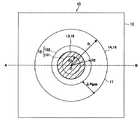
図1は、本実施形態に係る電子素子の要部の一例を示す断面図である。図2は、図1に図示する電子素子の平面図である。なお、図2の破線で示すA−B間での断面図が図1である。図2においては、絶縁膜等を一部省略している。 FIG. 1 is a cross-sectional view illustrating an example of a main part of an electronic device according to the present embodiment. FIG. 2 is a plan view of the electronic device shown in FIG. Note that FIG. 1 is a cross-sectional view taken along a broken line AB in FIG. In FIG. 2, the insulating film and the like are partially omitted.
電子素子10は、図1に図示するように、層間絶縁膜11、エッチング防止膜12、第1コンタクトホール13、第1電極14、支持膜15、第2電極16、ギャップ(空隙)17、絶縁膜18、および第2コンタクトホール19を有する。支持膜15は、多層化され、基体膜151および調整膜152で構成されている。
電子素子10は、図1に示すように両コンタクトホール13,19、および支持膜15がほぼ同一鉛直線上に配置され、図2に示すように両電極14,16の中心に配置されている。以下、各構成要素について述べる。
In the
層間絶縁膜11は、図1に示すように、図示しない半導体基板上に形成(成膜)されている。層間絶縁膜11は、絶縁性のシリコン酸化物(SiO2、以下SiO2と記す)で形成されているが、絶縁物であればその材質はいずれも特に限定されない。
半導体基板の構成等は特に限定されないが、後述の実施形態のように、半導体基板に下層配線層やトランジスタ等が好適に形成されている。As shown in FIG. 1, the
The configuration of the semiconductor substrate and the like are not particularly limited, but a lower wiring layer, a transistor, and the like are suitably formed on the semiconductor substrate as in the embodiments described later.
エッチング防止膜12は、エッチング防止のために、層間絶縁膜11上に形成されている。エッチング防止膜12は、絶縁性のシリコンナイトライド(SiN、以下SiNと記す)で形成されているが、たとえば酸化アルミニウム(アルミナ、Al2O3)で形成されていてもよく、絶縁物であればその材質はいずれも特に限定されない。The
第1コンタクトホール13は、第1電極14と図示しない半導体基板の配線層等とを電気的に接続(以下、単に接続という)するため、図1のように層間絶縁膜11およびエッチング防止膜12の一部に開口され、その内部にたとえば導電性のタングステン(W)が充填されている。第1コンタクトホール13は、図2の斜線部のように第1電極14の電極面の中心(中心O)付近に円形に開口されている。 Since the
第1電極14は、図1のようにエッチング防止膜12上に形成された図示しない下地層上に形成され、図2のように円形に形成されている。第1電極14の厚さH1は、30nm程度であり、その電極面積S1は好適に設定される。図2に図示するように第1電極14の電極半径Rは75nm程度に設定され、電極面積S1はπR2(πは円周率)により求まり、1.8×10³nm2程度である。第1電極14は、図示しない半導体基板の配線層等と接続するため、その電極面の中心で下地層を介して第1コンタクトホール13と接続されている。
第1電極14は、導電性の金(Au)で形成されているが、導電性の材質であれば特に限定されない。なお、厚さH1、電極半径Rは本実施形態に限定されない。The
The
支持膜15は、第1電極14と第2電極16とによる電極間(以下単に「電極間」という)にギャップ17を形成するために、図1のように第1電極14の電極表面上に、その半径方向の中心で膜厚が厚くなるように積層され、第2電極16を支持している。平面的には、支持膜15は、図2のように両コンタクトホール13,19の領域付近で膜厚が厚く(10nm〜12nm程度)、ギャップ17の内周側付近(半径R2程度の領域)では前者より膜厚が薄く(3nm〜7nm程度)形成されている。
このように半径方向の中心で膜厚を厚くするのは、電極間に所定の閾値電圧以上の電圧が印加された場合に、支持膜15の中心でのトンネル電流を抑制し、後述するギャップ17にのみトンネル電流を流すためである。本実施形態では、閾値電圧は、3.8V程度であり、膜厚は、支持膜15中のリーク電流を抑制するために、10nm程度以上が望ましい。
支持膜15は、絶縁性のSiO2で形成され、本実施形態では後述するように、基体膜151および調整膜152で構成された多層構造が採用されている。The
In this way, the film thickness is increased at the center in the radial direction by suppressing a tunnel current at the center of the
The
基体膜151は、図1のように第1電極14の表面上に絶縁性のSiO2で形成され、調整膜152によって当該支持膜が覆われている。基体膜151は、支持膜15の中心部に形成され、第2電極16を構造的に支える役割を果たす。具体的には、支持膜15は、図2のように中心Oから半径R1程度の領域に形成され、その膜厚は7nm程度である。
この半径R1は、両コンタクトホール13,19の半径より若干短い程度であるが、好適に設定可能であり、構造的に両電極の構造が維持できる程度のものであればよい。As shown in FIG. 1, the
The radius R1 is slightly shorter than the radii of the contact holes 13 and 19, but can be suitably set as long as it can structurally maintain the structure of both electrodes.
調整膜152は、図1のように支持膜151を覆うように絶縁性のSiO2で形成され、その形成面の上層は第2電極16に接している。調整膜152は、電極間の間隔を調整するための役割を果たす。具体的には、図2のように中心Oから半径R2程度の領域に形成され、その厚さは5nm程度である。
この半径R2は、ギャップ17の内周側付近の距離であるが、後述するエッチング処理によって好適に設定可能である。The
The radius R2 is a distance in the vicinity of the inner peripheral side of the
第2電極16は、図1のように支持膜15上、詳細には調整膜152上に形成され、図2のように第1電極14と同様に円形に形成されている。第2電極16の厚さH2は、30nm程度である。
詳細は後述するが、図2に図示するように、第2電極16は第1電極14と同一とみなせる程度の電極面積を有するため、第2電極16の半径は第1電極14の電極半径Rと同一とみなしてよい。第2電極16は、図示しない上層の配線層等と接続するため、その電極面の中心で第2コンタクトホール90と接続されている。
第2電極16は、導電性の金(Au)で形成されているが、導電性の材質であれば特に限定されない。なお、厚さH2は本実施形態に限定されない。The
Although details will be described later, as shown in FIG. 2, since the
The
ギャップ17は、図1のように第1電極14上の支持膜15が第2電極16を支持することによって生じたナノスケールのギャップである。ギャップ17は、図1に示すギャップ間隔Tgapおよび図2に示すギャップ幅ΔRgapを有し、支持膜15を中心として、ドーナツ状に形成され、ギャップ幅ΔRgapは電極半径Rの30%〜60%を占める。ギャップ間隔Tgapは、両電極14,16の材質や印加電圧等により好適に設定され、本実施形態では4nm程度である。ギャップ幅ΔRgapも好適に設定され、本実施形態では、40nm程度である。
電極間にこのようなギャップ17が形成され、所定の閾値電圧以上の電圧が電極間に印加されることで量子力学的なトンネル効果が発生し、電極間に(たとえば第2電極16から第1電極14へ)トンネル電流が流れる。
ギャップ間隔Tgapは、トンネル電流が流れ始める間隔より僅かに大きい必要があるが、ギャップ17を形成する電極間に電界が生じ、この電界による電極表面の金属原子の移動によってギャップ間隔Tgapが僅かに変化し、トンネル電流が容易に流れ始める程度の間隔でなければならない。The
Such a
The gap interval Tgap needs to be slightly larger than the interval at which the tunnel current begins to flow. However, an electric field is generated between the electrodes forming the
絶縁膜18は、図1のようにエッチング防止膜12上に両電極14,16および第2コンタクトホール19の周囲に形成されている。絶縁膜18は、絶縁性のSiO2で形成されているが、絶縁物であればその材質はいずれも特に限定されない。なお、図2においては、絶縁膜18の図示を省略している。As shown in FIG. 1, the insulating
第2コンタクトホール19は、第2電極16と図示しない上層の配線層等とを接続するため、図1のように絶縁膜18の一部に開口され、その内部にたとえば導電性のタングステン(W)が充填されている。第2コンタクトホール19は、図2の斜線部のように両電極14,16の電極面の中心(中心O)付近に円形に開口されている。 The
次に、上述した電子素子10の製造方法について、一例を挙げて説明する。
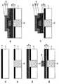
図3−1、3−2は、本実施形態に係る電子素子の製造方法を説明するための模式図である。なお、図3−1、3−2は図2の波線で示すA−B間での断面図である。Next, an example is given and demonstrated about the manufacturing method of the
3A and 3B are schematic views for explaining the method for manufacturing the electronic device according to the present embodiment. FIGS. 3A and 3B are cross-sectional views taken along a line AB in FIG.
(第1工程ST1)
図3−1(A)に図示しない半導体基板には、たとえばトランジスタや配線層が形成されている。図3−1(A)のように、この半導体基板のトランジスタ上に層間絶縁膜11となるSiO2の絶縁膜を酸化処理法、化学気相成長(CVD;Chemical Vapor Deposition)法のいずれかの方法で形成する。
上記と同様の方法にて、層間絶縁膜11上にエッチング防止膜12となるSiNの絶縁膜を形成する。
エッチング防止膜12は、後の工程でギャップ17の部分に形成されたSiO2の絶縁膜を薬液エッチングする際に、下層の層間絶縁膜11がエッチングされることを防ぐために形成されている。(First step ST1)
For example, transistors and wiring layers are formed on a semiconductor substrate (not shown in FIG. 3A). As shown in FIG. 3A, an SiO2 insulating film that becomes the interlayer insulating
A SiN insulating film to be the
The
(第2工程ST2)
図3−1(B)のように、層間絶縁膜11およびエッチング防止膜12の一部を開口し、その内部に導電性のタングステン(W)を充填し、エッチング防止膜12の表面を化学機械研磨等により平坦化する。(Second step ST2)
As shown in FIG. 3B, a part of the
(第3工程ST3)
図3−1(C)のように、エッチング防止膜12上に下地層110となるチタンの膜を化学気相成長法によって10nm程度形成する。
スパッタによる方法にて、下地層110上に第1電極14となる金の膜(層)を30nm程度形成する。(Third step ST3)
As shown in FIG. 3C, a titanium film serving as the
A gold film (layer) to be the
(第4工程ST4)
第1電極14上に基体膜151となるSiO2の絶縁膜を化学気相成長法よって7nm程度形成する。
次に、図3−1(D)のように、ホトリソグラフィ法、エッチング法等の方法によって、第2電極16を支持する部分以外を除去し、基体膜151を形成する。
なお、本工程で用いる方法は特に限定されない。(Fourth step ST4)
An SiO2 insulating film to be the
Next, as shown in FIG. 3D, the
Note that the method used in this step is not particularly limited.
(第5工程ST5)
図3−1(E)のように、基体膜151上を覆うように第1電極14上に調整膜152となるSiO2の絶縁膜をスパッタ法または化学気相成長法のいずれかの方法によって4nm程度形成する。調整膜152の膜厚を好適に調整することで、ギャップ間隔Tgapが4nm程度に調整される(図1を参照)。
上記と同様の方法にて、調整膜152上に第2電極16となる金の膜(層)を30nm程度形成する。
本工程を行うことにより、電極面が対向した両電極14,16が形成される。(Fifth step ST5)
As shown in FIG. 3E, an SiO2 insulating film serving as the
By the same method as described above, a gold film (layer) to be the
By performing this step, both
(第6工程ST6)
図3−1(F)のように、下地層110、第1電極14、基体膜151、調整膜152、および第2電極16で形成された積層膜(以下の工程の説明中では単に積層膜という)をホトリソグラフィ法、およびエッチング法等の方法により、所定の形状にエッチングする。本実施形態では、図2に示すような直径が150nm(電極半径R=75nm)程度の円形にエッチングする。
本工程では、同図のように一括加工するため、両電極14,16の電極面積は同一とみなせる。
なお、本工程で用いるエッチングの方法は特に限定されないが、金をエッチングする際には、イオンミリング法が望ましい。(6th process ST6)
As shown in FIG. 3-1 (F), a laminated film formed of the
In this step, the
Note that an etching method used in this step is not particularly limited, but an ion milling method is preferable when gold is etched.
(第7工程ST7)
図3−2(G)のように、基板全体(図3−1(F)に示す半導体基板および形成された膜全体)をフッ化水素(HF)の水溶液中に浸し、積層膜の側壁からフッ化水素を浸透させ、電極間の調整膜152の一部をエッチング法にて除去する。本実施形態では、両電極14,16の側壁から中心方向へ40nm程度、調整膜152を除去する。
これにより、ギャップ17が電極間に形成される。なお、本工程において、基体膜151の側面まで調整膜152を除去し、基体膜151の上層面にのみ調整膜152を残してもよい。エッチングの量は、薬液の濃度、温度、およびエッチングの時間を調整することで、好適に決定できる。(Seventh step ST7)
As shown in FIG. 3-2 (G), the entire substrate (the semiconductor substrate shown in FIG. 3-1 (F) and the entire formed film) is immersed in an aqueous solution of hydrogen fluoride (HF), and then from the side wall of the stacked film. Hydrogen fluoride is permeated and a part of the
Thereby, a
(第8工程ST8)
図3−2(H)のように、積層膜全体を覆うように、絶縁膜18となるSiO2の絶縁膜をたとえばプラズマCVD法によって形成する。
このとき、ギャップ17は、プラズマCVD法の被膜性能によりSiO2の絶縁膜が形成されず、ギャップが維持される。(Eighth step ST8)
As shown in FIG. 3-2 (H), an insulating film of SiO2 to be the insulating
At this time, the
(第9工程ST9)
図3−2(I)のように、絶縁膜18の表面を化学機械研磨等により平坦化し、絶縁膜18の一部を第2電極16の中心で開口し、その内部に導電性のタングステン(W)を充填する。(9th step ST9)
As shown in FIG. 3-2 (I), the surface of the insulating
(第10工程ST10)
図示しない他の回路の配線と共有した配線層等を一般的に行われている方法で形成する。(10th step ST10)
A wiring layer or the like shared with wiring of other circuits (not shown) is formed by a generally performed method.
たとえばギャップ間隔Tgapを7nm程度に変更する場合、図3−1(E)に示す第5工程ST5において、支持膜15を形成する調整膜152の膜厚のみを調整さればよい。この調整膜152による調整によってギャップ間隔Tgapが7nm程度に形成される。 For example, when the gap interval Tgap is changed to about 7 nm, only the film thickness of the
次に、電子素子10の動作例について説明する。
図4は、本実施形態に係る電子素子の動作例を説明するための図である。図5は、本実施形態に係る電子素子の動作例を示すタイミングチャートである。Next, an operation example of the
FIG. 4 is a diagram for explaining an operation example of the electronic device according to the present embodiment. FIG. 5 is a timing chart showing an operation example of the electronic device according to the present embodiment.
近接して形成された電極間に電圧を走印すると、図4に示す電流−電圧特性が現れる。図4中のA点付近の閾値電圧VthからO点付近の低電圧領域では、ギャップ17にトンネル電流が流れ、さらに電極間への印加電圧が大きくなる(AからC)と抵抗が大きくなる負性抵抗効果が現れ、ギャップ17にトンネル電流が流れにくくなる。本実施形態において、閾値電圧Vthは、3.6V程度である。
この抵抗変化は、急速に印加電圧をオフ(図4の0点付近)にしても保存される。たとえば、高電圧領域(A〜C)の電圧を両電極14,16に印加し、印加電圧を急速にオフにすれば、電子素子10が高抵抗状態、すなわちオフの状態が得られる。逆に、高電圧領域の電圧を両電極14,16に印加し、印加電圧をゆっくりオフにすれば、電子素子10が低抵抗状態、すなわちオンの状態が得られる。電子素子10のオン、オフは、印加電圧をオフにするまでの遷移時間を制御する。
このような特性は、ギャップ間隔Tgapが、トンネル電流が流れ始める近傍にある場合、電極間にかかる電界、あるいは電極間を流れる電流によって、金属電極の原子の一部が可逆的に移動し、それによって電極間のギャップがわずかに変化し、トンネル電流の流れやすさが変化するために生じる。When a voltage is imprinted between the electrodes formed close to each other, the current-voltage characteristic shown in FIG. 4 appears. In the low voltage region near the point O from the threshold voltageVth near the point A in FIG. 4, a tunnel current flows through the
This resistance change is preserved even when the applied voltage is rapidly turned off (near the 0 point in FIG. 4). For example, if a voltage in the high voltage region (A to C) is applied to both
Such a characteristic is that when the gap interval Tgap is in the vicinity of where the tunnel current begins to flow, a part of the atoms of the metal electrode reversibly move due to the electric field applied between the electrodes or the current flowing between the electrodes. This occurs because the gap between the electrodes slightly changes due to the change in the ease of tunneling current flow.
電子素子10は、高抵抗状態(オフの状態)を0、低抵抗状態(オンの状態)を1とすれば、デジタルのスイッチ素子として利用できる。以下に、具体的な電子素子10の動作例について説明する。 The
(電子素子10のオフ動作)
図5のように、時刻t1において、矩形パルス状のオフ電圧VOFFが電極間にかかるように両電極14,16に印加する。本実施形態において、オフ電圧VOFFは、たとえば6Vから10Vなど閾値電圧Vthより高い高電圧領域の電圧であり、時刻t1、t2間のパルス幅は、好適に設定され、パルスの立ち下がり時間は1ns程度が望ましい。(Off-operation of electronic element 10)
As shown in FIG. 5, at time t1, a rectangular pulse-like off voltage VOFF is applied to both
(読み出し動作)
時刻t2において、電極間の電位差が微小電圧になるように、読み出し電圧VRを両電極14,16に時刻t3まで印加する。その後、図1、2等に図示しない電流計にて電極間に流れる電流を検出する。電子素子10が高抵抗状態であるため、電極間に電流が流れず、電子素子10がオフの状態を検出できる。(Read operation)
At time t2, as the potential difference between the electrodes is very small voltage is applied to the time t3 a read voltageV R to the
(電子素子10のオン動作)
時刻t3において、矩形パルス状のオン電圧VONが電極間にかかるように両電極14,16に印加する。本実施形態において、オン電圧VONは、たとえば3.6V程度の閾値電圧Vthまたは、それよりわずかに高い電圧であり、時刻t3、t4間のパルス幅は、好適に設定され、100ns程度が望ましい。その後、緩やかに電圧を下げることでオン状態が書き込まれる。(ON operation of electronic element 10)
At time t3, a rectangular pulsed ON voltage VON is applied to both
(読み出し動作)
時刻t4において、電極間の電位差が微小電圧になるように、読み出し電圧VRを両電極14,16に時刻t5まで印加する。その後、前述の読み出し動作を行う。このとき、電子素子10が低抵抗状態であるため、電極間に電流が流れ、電子素子10がオンの状態を検出できる。(Read operation)
At time t4, as the potential difference between the electrodes is very small voltage is applied until time t5 a read voltageV R to the
オンの状態を得るためには、パルス状のオン電圧VONを両電極14,16に少なくとも100ns程度印加した後、緩やかに電圧を下げることが望ましい。読み出し電圧VRは、電極間の電流を検出できる程度の大きさである。In order to obtain an ON state, it is desirable to apply a pulsed ON voltage VON to both
以上詳細に説明したように、電子素子10は、第1電極14および第2電極16の電極面が対向して形成され、第1電極14の電極面上の一部に積層され、上記第2の電極の電極面を支持する多層構造で絶縁性の支持膜15と、支持膜15によって電極間の一部に形成されたトンネル電流が流れるギャップ17とを有し、両電極14,16の中心での膜厚がギャップ17付近のものよりも厚く形成されている。 As described above in detail, the
仮に、支持膜15の膜厚がギャップ17のギャップ間隔Tgapと同一の場合、微細なギャップ17を形成するために、支持膜15の厚さもある程度薄くしなければならない。
この場合、電極間に高電圧を加えるときに支持膜15中をトンネル電流が流れてしまったり、長期的には支持膜15の絶縁不良を招いたりする可能性があり、電子素子10の動作電圧に制限を加える必要が生じる。
具体的には、支持膜15の膜厚が4nm程度の場合、2V程度の電圧を電極間に印加するだけで支持膜15中に0.1nA/μm2程度の電流が流れてしまう。If the thickness of the
In this case, when a high voltage is applied between the electrodes, a tunnel current may flow in the
Specifically, when the thickness of the
そこで、本実施形態では、支持膜15の膜厚を微細なギャップ17のギャップ間隔Tgapよりも厚くすることで、支持膜15中のトンネル電流を抑え、信頼性を向上させている。
電子素子10への電圧の掛かり方、すなわちどれだけの時間、高電圧が電極間に印加されているかは、使用目的や回路構成によって異なり、酸化膜(支持膜15)の信頼性を考慮して好適に決定される。Therefore, in the present embodiment, the thickness of the
How the voltage is applied to the
(電子素子の第2実施形態)
本発明に係る電子素子の第2実施形態について説明する。本実施形態では、電子素子の第1実施形態と異なる点についてのみ説明する。(Second Embodiment of Electronic Device)
A second embodiment of the electronic device according to the present invention will be described. In the present embodiment, only differences from the first embodiment of the electronic device will be described.
図6は、本実施形態に係る電子素子の要部の一例を示す断面図である。
本実施形態は、図6に示す電子素子10aにおいて、支持膜15aが基体膜151aのみで形成され、その膜厚が前実施形態と異なる。この支持膜15aの膜厚が異なるため、ギャップ間隔Tgapも前実施形態と異なる。
詳細には、この支持膜15aの膜厚は、トンネル電流が流れ出す厚さ、すなわちトンネル電流を抑制可能な厚さよりわずかに厚く、支持膜15a全体が均一に形成されている。前実施形態での支持膜15の膜厚が10nm程度であったのに対し、本実施形態では、支持膜15aの膜厚が7nm程度に形成されている。この膜厚は、支持膜15a中のリーク電流を抑制する最小の厚さである。このため、ギャップ間隔Tgapも7nm程度に形成されている。FIG. 6 is a cross-sectional view illustrating an example of a main part of the electronic device according to the present embodiment.
In the present embodiment, in the
Specifically, the thickness of the
次に、上述した電子素子10aの製造方法について、一例を挙げて説明する。
図7は、本実施形態に係る電子素子の製造方法を説明するための模式図である。なお、図7は図2の波線で示すA−B間での断面図である。Next, an example is given and demonstrated about the manufacturing method of the
FIG. 7 is a schematic view for explaining the method for manufacturing the electronic device according to the present embodiment. FIG. 7 is a cross-sectional view taken along the line AB in FIG.
図3−1(A)〜(C)に示す工程ST1〜ST3と同様の工程を行った後、図7(A)のように、第1電極14上に基体膜151aとなるSiO2の絶縁膜を化学気相成長法よって7nm程度形成する。
続いて、図7(B)のように、基体膜151a上に第2電極16となる金の膜(層)をスパッタ法または化学気相成長法のいずれかの方法によって30nm程度形成する。
続いて、図7(C)のように、下地層110、第1電極14、基体膜151aおよび第2電極16で形成された積層膜をホトリソグラフィ法、およびエッチング法等の方法により、所定の形状にエッチングする。本実施形態では、図2に示すような直径が150nm(電極半径R=75nm)程度の円形にエッチングする。
その後の工程は、図3−2(G)〜(I)に示す工程ST7〜ST9およびST10と同様の工程を行う。After performing the same processes as the processes ST1 to ST3 shown in FIGS. 3-1 (A) to (C), as shown in FIG. 7 (A), insulation of SiO2 to be the
Subsequently, as shown in FIG. 7B, a gold film (layer) to be the
Subsequently, as shown in FIG. 7C, the laminated film formed of the
Subsequent steps are similar to steps ST7 to ST9 and ST10 shown in FIGS. 3-2 (G) to (I).
本実施形態では、ギャップ間隔Tgapが広すぎることによりトンネル電流が流れにくいことがある。この場合、電子素子10aを実際に使用する前の初期化の段階で、オン書き込み電圧を長時間(数ミリ秒程度)電極間に印加する。これにより、トンネル電流が増加し、電極表面上の原子の移動が起こり、ギャップ間隔Tgapの間隔が小さくなることで実用的に使用できる。 In this embodiment, the tunnel current may not flow easily due to the gap interval Tgap being too wide. In this case, an on-write voltage is applied between the electrodes for a long time (several milliseconds) at the initialization stage before actually using the
他の製造方法として、図7(C)に示す工程の後、ギャップ間隔Tgapを形成した状態で選択的に金のメッキ行う。詳細には、両電極14,16の露出部分(ギャップ17a部分)にだけ1nm程度の金メッキを行う。これにより、ギャップ間隔Tgapを狭めることが可能である。ギャップ間隔Tgapの間隔は、電極対向面全面に渡って必ずしも均一である必要は無く、ギャップ17aの領域でトンネル電流の流れやすさが変化すればよい。したがって、ごく薄い金のメッキの均一性について厳しい制御を要求されるわけではなく、電子素子10aを容易に製造できる。 As another manufacturing method, after the step shown in FIG. 7C, gold plating is selectively performed in a state where the gap interval Tgap is formed. Specifically, gold plating of about 1 nm is performed only on the exposed portions (gap 17a portion) of both
上述した2つの実施形態において、第1電極14および第2電極16は円形の電極を有するが、矩形、正方形、その他の形状であってもよい。両電極14,16が矩形の電極を有する場合について、第1実施形態に係る電子素子を例に挙げて説明する。 In the two embodiments described above, the
図8は、実施形態に係る電子素子の第1および第2の電極が矩形の電極を有する場合について説明する電子素子の平面図である。なお、図8の波線で示すC−D間での断面図が図1である。図8においては、絶縁膜等を一部省略している。 FIG. 8 is a plan view of the electronic device for explaining a case where the first and second electrodes of the electronic device according to the embodiment have rectangular electrodes. Note that FIG. 1 is a cross-sectional view taken along the line C-D shown by the wavy line in FIG. In FIG. 8, a part of the insulating film or the like is omitted.
図8のように、電子素子10bは、X軸方向の幅がW1、Y軸方向の幅がW2の第1電極14bおよび第2電極16bを有する。両電極14b,16bの形状に合わせて、第1コンタクトホール13b,第2コンタクトホール19b、支持膜15b(基体膜151b、調整膜152b)、およびギャップ17bの形状も矩形に形成されている。この場合、たとえば第6工程ST6において、図8に示す形状になるようにエッチングすればよい。 As shown in FIG. 8, the
(記憶装置の第1実施形態)
本発明に係る電子素子を採用した記憶装置の第1実施形態について説明する。以下に説明する記憶装置の実施形態では、電子素子の第1実施形態に係る電子素子を採用しているが、同第2実施形態に係る電子素子を採用してもよい。(First Embodiment of Storage Device)
A first embodiment of a storage device employing an electronic element according to the present invention will be described. In the embodiment of the storage device described below, the electronic element according to the first embodiment of the electronic element is employed, but the electronic element according to the second embodiment may be employed.
図9は、本実施形態に係る記憶装置の一例を示す断面図である。図10は、図9に図示する記憶装置の平面図である。なお、図9,10では、絶縁膜や下地層等、一部を省略している。 FIG. 9 is a cross-sectional view showing an example of the storage device according to the present embodiment. 10 is a plan view of the storage device shown in FIG. 9 and 10, some of the insulating film, the base layer, and the like are omitted.
記憶装置20は、図9のように電子素子10、下層配線層(第1の配線層)21、上層配線層(第2の配線層)22、絶縁層23および24を有する。前記の各構成要素によって、セルCELが構成されている。
記憶装置20は、図10のように第1の電圧供給回路としての列選択回路(HSEL)30および第2の電圧供給回路としての行選択回路(VSEL)40を有する。As shown in FIG. 9, the
The
セルCELは、図10のようにマトリクス状に配列されている。図中では、説明の簡略化のため、行方向に3個、列方向に4個、合計12個のセルCELが配列されているとする。以下、i(=1,2,…)行、j(=1,2,…)列目のセルをCEL(i、j)のように適宜表記する。後述する下層配線層21および上層配線層22についても、下層配線層21(j)、上層配線層22(i)のように適宜表記する。
同一行のセルCEL(たとえばセルCEL(1、j))は、セルCEL中の第2電極16と第2コンタクトホール19を介して接続された上層配線層22(たとえば上層配線層22(1))に共通に接続されている。
同一列のセルCEL(たとえばセルCEL(i、1))は、セルCEL中の第1電極14と第1コンタクトホール13を介して接続された下層配線層21(たとえば下層配線層21(1))に共通に接続されている。The cells CEL are arranged in a matrix as shown in FIG. In the figure, for simplification of explanation, it is assumed that a total of 12 cells CEL are arranged, 3 in the row direction and 4 in the column direction. Hereinafter, a cell in the i (= 1, 2,...) Row and j (= 1, 2,...) Column is appropriately expressed as CEL (i, j). The
A cell CEL (for example, cell CEL (1, j)) in the same row has an upper wiring layer 22 (for example, upper wiring layer 22 (1)) connected to the
Cells CEL in the same column (for example, cell CEL (i, 1)) are connected to the
下層配線層21は、図9のように電子素子10の第1電極14と第1コンタクトホール13を介して接続され、第1コンタクトホール13との接続部分以外が絶縁層23または層間絶縁膜11で覆われている。下層配線層21は、アルミニウム(Al)で形成されているが、導電性の材質であれば特に限定されない。
同一列の下層配線層21(たとえば下層配線層21(1))は、図10のように、同一列のセルCEL(たとえばセルCEL(i、1))中の第1電極14と第1コンタクトホール13を介して共通に接続され、一端が列選択回路30に接続されている。As shown in FIG. 9, the
As shown in FIG. 10, lower wiring layer 21 (for example, lower wiring layer 21 (1)) in the same column is connected to
上層配線層22は、図9のように電子素子10の第2電極16と第2コンタクトホール19を介して接続され、第2コンタクトホール19との接続部分以外が絶縁層24または絶縁膜18で覆われている。上層配線層22は、アルミニウム(Al)で形成されているが、導電性の材質であれば特に限定されない。
同一行の上層配線層22(たとえば上層配線層22(1))は、図10のように、同一行のセルCEL(たとえばセルCEL(1、j))中の第2電極16と第2コンタクトホール19を介して共通に接続され、一端が行選択回路40に接続されている。The
As shown in FIG. 10, the upper wiring layer 22 (for example, the upper wiring layer 22 (1)) in the same row is connected to the
絶縁層23は、図9のように、下層配線層21を覆うように絶縁性のSiO2で形成されている。As shown in FIG. 9, the insulating
絶縁層24は、図9のように、上層配線層22を覆うように絶縁性のSiO2で形成されている。As shown in FIG. 9, the insulating
列選択回路30は、列方向の下層配線層21がそれぞれ接続され、対象となる(書き込みまたは消去を行う)セルCELが接続されている行の下層配線層21に所定の電圧(第1の電圧)を印加する。具体的には、列選択回路30は、対象となる電子素子10に書き込みをする場合は書き込み電圧VHWを、同素子の状態を読み出す場合は読み出し電圧VHRを、同素子の状態を消去する場合は消去電圧VHDを下層配線層21に印加する。列選択回路30は、対象外の電子素子10に対しては電圧VHLを下層配線層21に印加する。この詳細については後述する。In the
行選択回路40は、行方向の上層配線層22がそれぞれ接続され、対象となるセルCELが接続されている行の上層配線層22に所定の電圧(第2の電圧)を印加する。具体的には、行選択回路40は、対象となる電子素子10に書き込みをする場合は書き込み電圧VVWを、同素子の状態を読み出す場合は読み出し電圧VVRを、同素子の状態を消去する場合は消去電圧VVDを上層配線層22に印加する。行選択回路40は、対象外の電子素子10に対しては電圧VVLを上層配線層22に印加する。この詳細については後述する。The
次に、記憶装置20の動作の一例について、図11を参照しながら説明する。
図11は、本実施形態に係る記憶装置のタイミングチャートである。図11中のHSEL(i)は列選択回路30が出力する電圧を、VSEL(j)は行選択回路40が出力する電圧をそれぞれ示している。Next, an example of the operation of the
FIG. 11 is a timing chart of the storage device according to the present embodiment. In FIG. 11, HSEL (i) indicates a voltage output from the
本実施形態において、説明を簡単にするために、セルCEL(3,2)に対して(電圧の)書き込みおよび消去を行い、全セルCELからその状態を読み出すものとする。図11の時刻t1以前において、電子素子10はオフの状態であるものとする。 In this embodiment, in order to simplify the description, it is assumed that (voltage) writing and erasing are performed on the cell CEL (3, 2), and the state is read from all the cells CEL. It is assumed that the
(書き込み動作)
時刻t1において、列選択回路30は、下層配線層21(3)に書き込み電圧VHWを印加し(図11(C))、その他の下層配線層21には電圧VHLを印加し(図11(A)、(B),(D))、時刻t2までその電圧をそれぞれ保持する。本実施形態では、書き込み電圧VHWは接地電圧(0V)程度、電圧VHLは3V程度である。
同時刻において、行選択回路40は、上層配線層22(2)に書き込み電圧VVWを印加し(図11(F))、その他の上層配線層22には電圧VVLを印加し(図11(E)、(G))、時刻t2までその電圧をそれぞれ保持する。本実施形態では、書き込み電圧VVWは閾値電圧Vth(=3.6V程度)より高い4V程度、電圧VVLは3V程度である。時刻t1、t2間の書き込み時間は、好適に設定されるが、少なくとも100ns程度以上で電圧立ち下がり時間が50ns程度以上が望ましい。
これにより、セルCEL(3,2)の(対向した両電極14,16の)電極間には4Vの電圧(電位差)が、他のセルCELの電極間には0V、1V程度または3V程度の電圧がかかっている。たとえばセルCEL(1,1)の電極間には0V程度の電圧が、セルCEL(3,3)の電極間には1V程度の電圧がかかっている。
換言すれば、電極間に閾値電圧Vth付近(図4のB点付近)の電圧が所定時間(100ns程度)印加されたセルCEL(3,2)の電子素子10のみがオンの状態に切り替わり、他のセルの電子素子10はオフの状態が保持される。(Write operation)
At time t1, the
At the same time, the
As a result, a voltage (potential difference) of 4 V is provided between the electrodes of the cell CEL (3, 2) (of the opposing
In other words, only the
(読み出し動作)
時刻t2において、列選択回路30は、一つの列の下層配線層21に対して読み出し電圧VHRを印加し、他の下層配線層21には0Vを時刻t3まで印加する。行選択回路40は、全ての行の上層配線層22に0Vを時刻t3まで印加する。各行に対応する上層配線層22に流れる電流は、列選択回路30が選択した列の下層配線層21に繋がる各セルCELのオン、オフに対応した電流となる。
したがって、図11に図示するように、列選択回路30が下層配線層21(3)を選択すると、下層配線層21(3)に繋がる各々セルCELの両電極間に電流が流れ、この電流を図9,10に図示しない電流計にて各々セルCELから読み出す。このとき、各々セルCELから書き込まれた電圧に対応した電流が検出され、各々電子素子10の抵抗が高い状態か低い状態かが検出できる。
この時、セルCEL(3,2)だけがオン状態に書き込まれているため、上層配線層22(2)に流れる電流だけが大きくなる。
すなわち、セルCEL(3,2)の電子素子10のみから、低い抵抗状態が検出され、オンの状態であることが検出できる。
以下同様に、列選択回路30が他の下層配線層21を順次選択し、その時のそれぞれの上層配線層22に流れる電流を読み出すことで、全セルCELの状態を検出する。(Read operation)
At time t2, the
Therefore, as shown in FIG. 11, when the
At this time, since only the cell CEL (3, 2) is written in the ON state, only the current flowing through the upper wiring layer 22 (2) increases.
That is, a low resistance state is detected only from the
Similarly, the
(消去動作)
時刻t3において、列選択回路30は、下層配線層21(3)に消去電圧VHDを印加し(図11(C))、その他の下層配線層21には電圧VHLを印加し(図11(A)、(B),(D))、時刻t4までその電圧をそれぞれ保持する。本実施形態では、消去電圧VHDは接地電圧(0V)程度である。
同時刻において、行選択回路40は、上層配線層22(2)に消去電圧VVDを印加し(図11(F))、その他の上層配線層22には電圧VVLを印加し(図11(E)、(G))、時刻t4までその電圧をそれぞれ保持する。
本実施形態では、消去電圧VVDは書き込み電圧VVWより高い電圧(たとえば図4のC点付近の電圧で、6V程度)である。時刻t3、t4間の消去時間は、好適に設定されるが、1ns程度が望ましい。
これにより、セルCEL(3,2)の電極間にのみ消去電圧VHD電圧が、他のセルCELの電極間には0V、または3V程度の電圧がかかっている。たとえばセルCEL(1,1)の電極間には0V程度の電圧が、セルCEL(3,3)の電極間には3V程度の電圧が、かかっている。
換言すれば、電極間に閾値電圧Vthより高い(図4のC点付近)電圧が印加され、その後急峻に電圧が切られたセルCEL(3,2)の電子素子10のみがオフの状態に切り替わり、他のセルの電子素子10は引き続きオフの状態が保持される。(Erase operation)
At time t3, the
At the same time, the
In this embodiment, the erase voltage VVD is higher than the write voltage VVW (for example, a voltage near the point C in FIG. 4 and about 6 V). The erasing time between times t3 and t4 is preferably set, but is preferably about 1 ns.
As a result, the erase voltage VHD voltage is applied only between the electrodes of the cell CEL (3, 2), and a voltage of about 0 V or 3 V is applied between the electrodes of the other cells CEL. For example, a voltage of about 0 V is applied between the electrodes of the cell CEL (1, 1), and a voltage of about 3 V is applied between the electrodes of the cell CEL (3, 3).
In other words, only the
(読み出し動作)
時刻t4からt5における読み出し動作は、前述のものと同様の手順で行う。
これにより、全てのセルCELから高い抵抗状態が検出され、オフの状態であることが検出できる。(Read operation)
The read operation from time t4 to t5 is performed in the same procedure as described above.
Thereby, a high resistance state is detected from all the cells CEL, and it can be detected that the cell is in an OFF state.
上述したように、対象となるセルCELに、電子素子10の抵抗変化が起こる電圧(書き込み時には閾値電圧Vth付近の電圧を長期間、消去時には閾値電圧Vthより高い電圧を短期間)が電極間にかかるように、両電極14,16間に印加すればよい。対象外のセルCELには、閾値電圧Vth付近以下の電圧が電極間にかかるように、両電極14,16間に印加すればよい。
以上述べたように、本実施形態が電子素子10を採用した記憶装置の基本構成である。As described above, the voltage at which the resistance change of the
As described above, this embodiment is a basic configuration of a storage device that employs the
(記憶装置の第2実施形態)
本発明に係る電子素子を採用した記憶装置の第2実施形態について説明する。本実施形態では、記憶装置の第1実施形態と異なる点を中心に説明する。(Second Embodiment of Storage Device)
A second embodiment of a storage device employing the electronic element according to the present invention will be described. In the present embodiment, a description will be given focusing on differences from the first embodiment of the storage device.
図12は、本実施形態に係る記憶装置の一例を示す断面図である。図13は、図12に図示する記憶装置の等価回路図である。なお、図12では、下地層等、一部を省略している。 FIG. 12 is a cross-sectional view showing an example of the storage device according to the present embodiment. FIG. 13 is an equivalent circuit diagram of the storage device shown in FIG. In FIG. 12, a part of the base layer is omitted.
記憶装置20aは、図12のように電子素子10、n型のソース層21a、第1上層配線層22(第1の配線層)a、絶縁層23,24、n型のドレイン層25、ゲート電極26、p型の半導体基板27、第3コンタクトホール28、第2上層配線層(第2の配線層)29、およびゲート配線層(第3の配線層)210(不図示)を有する。
ソース層21a、ドレイン層25、ゲート電極26、および半導体基板27によってトランジスタとしてのnチャネルMOSFET(Metal Oxide Semiconductor Field Effect Transistor;以下NMOS)が構成されている。前記の各々構成要素によってセルCELaが構成されている。
記憶装置20aは、図13のようにゲート配線層210、第1の電圧回路としての列選択回路(HSEL)30a、行選択回路(VSEL)40a、およびデータ選択検出回路(DSEL)50を有する。As shown in FIG. 12, the
The
As shown in FIG. 13, the
本実施形態では、第1電極14が第1コンタクトホール13を介してソース層21aに接続されている。図13のように、電子素子10の第1電極14がNMOSのソースに接続され、列選択回路30a、および行選択回路40aにて対象のセルCELaの選択を行う。以下、前実施形態と異なる構成要素について説明する。 In the present embodiment, the
セルCELaは、図13のようにマトリクス状に配列されている。図中では、説明の簡略化のため、行方向に2個、列方向に4個、合計8個のセルCELaが配列されているとする。
同一行のセルCELa(たとえばセルCELa(1、j))は、セルCELa中の第1上層配線層22a(たとえば第1上層配線層22a(1))が共通に接続され、第2上層配線層29(たとえば第2上層配線層29(1))が共通に接続されている。
同一列のセルCELa(たとえばセルCELa(i、1))は、セルCELa中のゲート電極26がゲート配線層210(たとえばゲート配線層(1))に共通に接続されている。The cells CELa are arranged in a matrix as shown in FIG. In the figure, for simplification of explanation, it is assumed that a total of eight cells CELa are arranged, two in the row direction and four in the column direction.
Cells CELa (for example, cell CELa (1, j)) in the same row are commonly connected to first upper
In cells CELa (for example, cell CELa (i, 1)) in the same column,
ソース層21aは、p型の半導体基板27上に形成されたn型のシリコン領域で、第1コンタクトホール13を介して第1電極14と接続されている。ソース層21aは、半導体基板27側の一部が隣り合うセルCELaのドレイン層25と絶縁層23で絶縁され、電子素子10側の一部が層間絶縁膜11で覆われている。 The
ドレイン層25は、p型の半導体基板27上に形成されたn型のシリコン領域で、第3コンタクトホール28を介して第2上層配線層29と接続されている。ドレイン層25は、半導体基板27側の一部が隣り合うセルCELのソース層21aと絶縁層23で絶縁され、電子素子10側の一部が層間絶縁膜11で覆われている。 The
ゲート電極26は、その周囲が層間絶縁膜11で覆われ、図13のようにゲート配線層210として列選択回路30aと接続されている。 The periphery of the
半導体基板27部分は、p型のシリコンで形成されたpウェルになっており、上層にソース層21aおよびドレイン層25が形成され、隣り合うソース層21aとドレイン層25とを絶縁するように絶縁層23が形成されている。 The
第3コンタクトホール28は、ドレイン層25と第2上層配線層29とを接続するため、層間絶縁膜11、エッチング防止膜12,絶縁膜18の一部に開口され、その内部にたとえば導電性のタングステンが充填されている。 The
第2上層配線層29は、NMOSのドレイン層25と第3コンタクトホール28を介して接続され、第3コンタクトホール28との接続部分以外が絶縁層24で覆われている。第2上層配線層29は、アルミニウムで形成されているが、導電性の材質であれば特に限定されない。
同一行の第2上層配線層29(たとえば第2上層配線層29(1))は、図12のように、同一行のセルCELa(たとえばセルCELa(1、j))中のドレイン層25と第3コンタクトホール28を介して共通に接続され、図13のように一端がデータ選択検出回路50に接続されている。The second
As shown in FIG. 12, second upper wiring layer 29 (for example, second upper wiring layer 29 (1)) in the same row is connected to drain
同一列のゲート配線層210(たとえばゲート配線層210(1))は、図13のように、同一列のセルCELa(たとえばセルCELa(1、j))中のゲート電極26と共通に接続され、一端が列選択回路30aに接続されている。 Gate wiring layer 210 (for example, gate wiring layer 210 (1)) in the same column is commonly connected to
NMOSは、図13のように、ソースが電子素子10の第1電極14に、ドレインがデータ選択検出回路50に、ゲートが列選択回路30aにそれぞれ接続されている。NMOSは、電子素子10がオン(両電極間14,16にトンネル電流が流れる)の状態で第2上層配線層29すなわちドレイン層25に所定電圧が、ゲート電極26に電圧が印可されると、電子素子10からソース層21aを通してドレイン層25に電流が流れる。 As shown in FIG. 13, the NMOS has a source connected to the
列選択回路30aは、列方向のゲート配線層210がそれぞれ接続され、対象となるセルCELaが接続されている列のゲート配線層210にNMOSがオンとなる電圧を印加する。 The
行選択回路40aは、行方向の第1上層配線層22aがそれぞれ接続され、対象となるセルCELaが接続されている行の第1上層配線層22aに所定の電圧(書き込み電圧VVW、読み出し電圧VVR、消去電圧VVD、電圧VVLのいずれか)を印加する。In the
データ選択検出回路50は、行方向の第2上層配線層29がそれぞれ接続され、対象となるセルCELaに流れる電流を検出する回路(不図示)に接続されている。データ選択検出回路50が第2上層配線層29に印加する電位は基本的に0Vである。 The data
次に、記憶装置20aの動作の一例について説明する。図14は、本実施形態に係る記憶装置のタイミングチャートである。図14中のHSEL(i)は列選択回路30aが出力する電圧を、VSEL(j)は行選択回路40aが出力する電圧をそれぞれ示している。本実施形態において、説明を簡単にするために、セルCELa(1,1)に対して書き込み、読み出しおよび消去を行うものとして説明する。 Next, an example of the operation of the
(書き込み動作)
時刻t1において、列選択回路30aは、ゲート配線層210(1)に選択信号としての電圧VHを印加し(図14(A))、その他のゲート配線層210には非選択なので0Vの電圧を印加し(図14(B)〜(D))、時刻t2までその電圧をそれぞれ保持する
同時刻において、行選択回路40aは、第1上層配線層22a(1)に書き込み電圧VVWを印加し(図14(E))、その他の第1上層配線層22aには0Vの電圧を印加し(図14(F))、時刻t2までその電圧をそれぞれ保持する。本実施形態では、電圧VHは電源電圧VDD、書き込み電圧VVWは閾値電圧Vth(=3.6V程度)より高い4V程度である。その後、列選択回路30aは、書き込み電圧VVWを緩やかに低下させる。
同時刻において、データ選択検出回路50は、すべての第2上層配線層29に0Vの電圧を印加し、すべての時刻(t1〜t8)に亘ってその電圧をそれぞれ保持する(不図示)。
本実施形態では、書き込み動作、読み出し動作および消去動作の各サイクル間(t2〜t3、t4〜t5、t6〜t7)に、短いスタンバイ期間を設けている。(Write operation)
At time t1, the
At the same time, the data
In this embodiment, a short standby period is provided between the cycles of the write operation, the read operation, and the erase operation (t2 to t3, t4 to t5, t6 to t7).
(読み出し動作)
時刻t3において、列選択回路30aは、ゲート配線層210(1)に電圧VHを印加し(図14(A))、その他のゲート配線層210には0Vの電圧を時刻t4まで印加する(図14(B)〜(D))。
同時刻において、行選択回路40aは、第1上層配線層22a(1)に読み出し電圧VVRを、その他の第1上層配線層22aには0Vの電圧を時刻t4まで印加する(図14(E)、(F))。
本実施形態において、読み出し電圧VVRは、電子素子10の抵抗を測定できる、状態変化の閾値電圧Vthより十分に低い電位(1V程度)である。
この時、データ選択検出回路50がセルCEL(1,1)に流れる電流を第2上層配線層29(1)から読み出し、図示しない回路にて電流を検出する。
以下同様に、列選択回路30aが他のゲート配線層210を、行選択回路40aが他の第1上層配線層22aを順次選択し、その時のそれぞれの第2上層配線層29に流れる電流を読み出すことで、全セルCELの状態を検出する。(Read operation)
At time t3, the
At the same time, the
In the present embodiment, the read voltageVVR is a potential (about 1 V) that is sufficiently lower than the threshold voltageVth of the state change that can measure the resistance of the
At this time, the data
Similarly, the
(消去動作)
時刻t5において、列選択回路30aは、ゲート配線層210(1)に電圧VHを印加し(図14(A))、その他のゲート配線層210(1)には0Vの電圧を印加し(図14(B)〜(D))、時刻t6までその電圧をそれぞれ保持する。
同時刻において、行選択回路40aは、第1上層配線層22a(1)に消去電圧VVDを印加し(図14(E))、その他の第1上層配線層22には0Vの電圧を印加し(図14(F))、時刻t6までその電圧をそれぞれ保持した後急峻に消去電圧VVDをオフにする。
本実施形態では、消去電圧VVDは書き込み電圧VVWより高い電圧である。(Erase operation)
At time t5, the
At the same time, the
In the present embodiment, the erase voltage VVD is higher than the write voltage VVW .
本実施形態では、第1、第2上層配線層に印加する電圧を制限して非選択セルへの影響を制限する必要がないため、回路構成や動作の自由度が向上できる。 In this embodiment, it is not necessary to limit the voltage applied to the first and second upper wiring layers to limit the influence on the non-selected cells, so that the circuit configuration and the degree of freedom of operation can be improved.
(記憶装置の第3実施形態)
本発明に係る電子素子を採用した記憶装置の第3実施形態について説明する。本実施形態では、記憶装置の第1実施形態と異なる点を中心に説明する。(Third embodiment of storage device)
A third embodiment of a storage device employing the electronic element according to the present invention will be described. In the present embodiment, a description will be given focusing on differences from the first embodiment of the storage device.
図15は、本実施形態に係る記憶装置の一例を示す断面図である。図16は、図15に図示する記憶装置の等価回路図である。なお、図15では、絶縁膜や下地層等、一部を省略している。 FIG. 15 is a cross-sectional view illustrating an example of the storage device according to the present embodiment. FIG. 16 is an equivalent circuit diagram of the storage device shown in FIG. In FIG. 15, some of the insulating film, the base layer, and the like are omitted.
記憶装置20bは、図15のように電子素子10、n型拡散層21b、p型拡散層212、上層配線層(第1の配線層)22、絶縁層23、24、213を有する。n型拡散層21b、および列選択線としてのp型拡散層212によってPN接合のダイオードPNが構成されている。前記の各々構成要素によってセルCELbが構成されている。
記憶装置20bは、図16のように第1の電圧供給回路としての列選択回路(HSEL)30b、第2の電圧供給回路としての行選択回路(VSEL)40b、および配線層(第2の配線層)212を有する。As shown in FIG. 15, the
As shown in FIG.16 , the
本実施形態では、第1電極14がダイオードのn型拡散層21bに接続されている。以下、記憶装置の第1実施形態と異なる構成要素について説明する。 In the present embodiment, the
セルCELbは、図16のようにマトリクス状に配列されている。図中では、説明の簡略化のため、行方向に2個、列方向に4個、合計8個のセルCELbが配列されているとする。
同一列のセルCELb(たとえばセルCELb(i、1))は、セルCELb中のp型拡散層212が配線層213(たとえばゲート配線層(1))に共通に接続されている。The cells CELb are arranged in a matrix as shown in FIG. In the figure, for simplification of description, it is assumed that a total of eight cells CELb are arranged, two in the row direction and four in the column direction.
In cells CELb (for example, cell CELb (i, 1)) in the same column, p-
n型拡散層21bは、p型拡散層212上に形成されたn型のシリコン領域で、第1コンタクトホール13を介して第1電極14と接続されている。n型拡散層21bは、第1コンタクトホール13およびp型拡散層212と接する面以外が絶縁層23,213で絶縁されている。 The n-
p型拡散層212は、絶縁層214上に形成されたp型のシリコン領域で、n型拡散層21bと接続されている。p型拡散層212は、n型拡散層21bと接する面以外が絶縁層23,214で絶縁されている。p型拡散層212は、図16のように列選択回路30bに接続されている。 The p-
ダイオードPNは、図16のように、p型拡散層212(アノード)が列選択回路30bに、n型拡散層21b(カソード)が電子素子10の第1電極14に接続され、順方向バイアスを印可するとp型拡散層212からn型拡散層21bを通して電子素子10へ電流が流れる。 As shown in FIG. 16, the diode PN has a p-type diffusion layer 212 (anode) connected to the
本実施形態では、記憶装置の第1実施形態と同様の動作を行う。たとえば、セルb(1,1)に着目すれば、書き込み動作、読み出し動作、および消去動作は次のように実行すればよい。
書き込み動作においては、列選択回路30bがp型拡散層212(1)に4V程度の電圧を印可し、他のp型拡散層212(1)には0V程度の電圧を印可するようにし、行選択回路40bが上層配線層22(1)に0V程度を、他の上層配線層22には4Vの電圧を印可するようにする。
このとき、選択されたセルCEL(1,1)では、電子素子10にバイアスがかかり、オン書き込みがなされる。非選択のセルCELでは、電子素子10とダイオードPNにかかる電圧は0V、あるいは4V程度であるが、4V程度であってもダイオードPNが逆バイアスとなり電流が流れないため、書き込みが行われない。
読み出し動作においては、列選択回路30bがp型拡散層212(1)にのみ2V程度の電圧を印可し、他のp型拡散層212に0V程度の電圧を印可し、行選択回路40bが上層配線層22に0V程度の電圧を印可するようにする。これにより、セルCELに流れる電流を列選択線(p型拡散層212)で読み出せばよい。
消去動作においては、列選択回路30bがp型拡散層212(1)に6V程度の高い電圧を印可し、他のp型拡散層212(1)に0V程度の電圧を印可し、行選択回路40bが上層配線層22に0V程度の電圧を、非選択の上層配線層22には4V程度の電圧を印可するようにする。その後、急激に印加電圧を取り去れば、対象となるセルCEL(1,1)へのゼロ書き込み、すなわち消去ができる。In this embodiment, the same operation as that of the first embodiment of the storage device is performed. For example, focusing on the cell b (1, 1), the write operation, the read operation, and the erase operation may be executed as follows.
In the write operation, the
At this time, in the selected cell CEL (1, 1), the
In the read operation, the
In the erase operation, the
このように、本実施形態では、セルCELbの選択にp型拡散層212からn型拡散層21bへ電流が流れるダイオードを用いたため、記憶装置の第2実施形態よりもセル面積を縮小できる。 As described above, in this embodiment, since the diode in which a current flows from the p-
以下に、本発明の実施形態に係る電子素子の利点を述べる。
実施形態に係る電子素子は、その構造および製造が極めて単純であり、安定した不揮発性のスイッチ動作を実行できる。
2つの電極が同一鉛直線方向に積層されているので、電子素子の占有面積が他の構造のものと比較して極めて小さい利点がある。
支持膜の厚さを調整することでギャップの間隔を調整できるため、高精度かつ高再現性の製造が行え、その際に、一般的な半導体集積回路の製造プロセスを使用できる利点がある。
電極の加工が一回のホトリソグラフィとエッチングの工程で行う得るため、生産性が優れる。
2つの電極を支持する支持膜(SiO2)の厚さがギャップ間隔より大きくとられているため、電極間の余分なリーク電流が抑えられ、支持膜の長期信頼性が優れている。
ギャップ部分が絶縁膜で覆われた構造であるため、電子素子自体を汚染やショートから保護しやすい利点がある。
本発明の実施形態に係る電子素子は、半導体集積回路との親和性が高く、容易に半導体回路と一体形成ができる。
電子素子の下部にSiO2とのエッチング選択比の高いSiN膜あるいはアルミナ膜が使用されているため、ギャップのエッチング工程が他の部分に悪影響を与えることを防止する利点がある。Hereinafter, advantages of the electronic device according to the embodiment of the present invention will be described.
The electronic device according to the embodiment is extremely simple in structure and manufacture, and can perform a stable nonvolatile switch operation.
Since the two electrodes are stacked in the same vertical direction, there is an advantage that the area occupied by the electronic element is extremely small compared to other structures.
Since the gap interval can be adjusted by adjusting the thickness of the support film, high-precision and high-reproducibility manufacturing can be performed, and there is an advantage that a general semiconductor integrated circuit manufacturing process can be used.
Productivity is excellent because the electrode can be processed by a single photolithography and etching process.
Since the thickness of the support film (SiO2 ) supporting the two electrodes is larger than the gap interval, excessive leakage current between the electrodes can be suppressed, and the long-term reliability of the support film is excellent.
Since the gap portion is covered with an insulating film, there is an advantage that the electronic device itself can be easily protected from contamination and short circuit.
The electronic device according to the embodiment of the present invention has high affinity with a semiconductor integrated circuit, and can be easily formed integrally with a semiconductor circuit.
Since an SiN film or an alumina film having a high etching selection ratio with SiO2 is used below the electronic element, there is an advantage of preventing the gap etching process from adversely affecting other portions.
以下に、本発明の実施形態に係る記憶装置の利点を述べる。
電子素子を上下層配線層間に配置しているため、電子素子をマトリクス状に配置することが容易である。
電子素子に独立した高抵抗状態または低抵抗状態を設定できるため、メモリとしての活用が容易である。
電子素子とトランジスタ(MOSFET)が直列に接続されたセルがマトリクス状に配置されているため、各配線層の電位(電圧)制御によりデータの書き込み、読み出し、消去等の制御が自由にできる。
電子素子とダイオードが直列に接続されたセルがマトリクス状に配置されているため、各配線層の電位(電圧)制御によりデータの書き込み、読み出し、消去等の制御の自由に行える。The advantages of the storage device according to the embodiment of the present invention will be described below.
Since the electronic elements are arranged between the upper and lower wiring layers, it is easy to arrange the electronic elements in a matrix.
Since the electronic element can be set to a high resistance state or a low resistance state, it can be easily used as a memory.
Since cells in which electronic elements and transistors (MOSFETs) are connected in series are arranged in a matrix, data writing, reading, erasing, and the like can be freely controlled by controlling the potential (voltage) of each wiring layer.
Since cells in which electronic elements and diodes are connected in series are arranged in a matrix, data writing, reading, erasing, and the like can be freely controlled by controlling the potential (voltage) of each wiring layer.
本発明は、本発明の要旨を変更しない範囲内で様々な改変が可能である。
本実施形態の説明では、説明を簡単化するためにトランジスタやダイオードに関わる内部電圧降下について省略した。本発明を適用の際には、それらの電圧降下や寄生抵抗などを考慮した電圧の設定等が必要である。The present invention can be modified in various ways without departing from the scope of the present invention.
In the description of this embodiment, the internal voltage drop related to the transistor and the diode is omitted for the sake of simplicity. When applying the present invention, it is necessary to set a voltage in consideration of such a voltage drop and parasitic resistance.
10、10a、10b…電子素子、11…層間絶縁膜、12…エッチング防止膜、13…第1コンタクトホール、14、14b…第1電極、15、15a、15b…支持膜、16、16b…第2電極、17、17a、17b…ギャップ、18…絶縁膜、19、19b…第2コンタクトホール、20、20a、20b…半導体装置、21…下層配線層、21a…ソース層、21b…n型拡散層、22…上層配線層、22a…第1上層配線層、23、24…絶縁層、25…ドレイン層、26…ゲート電極、27…半導体基板、28…第3コンタクトホール、29…第2上層配線層、30、30a、30b…列選択回路、40、40a、40b…行選択回路、50…データ選択回路、110…下地層、151、151a、151b…基体膜、152…調整膜、210…ゲート配線層、212…p型拡散層、213…配線層、214…絶縁層、CEL、CELa、CELb…セル、Tgap…ギャップ間隔、ΔRgap…ギャップ幅、R…電極半径、R1、R2…半径、S1…電極面積。 DESCRIPTION OF
Claims (14)
Translated fromJapanese上記第1の電極の一方の面上の中心部に位置する、絶縁性の支持膜と、
一方の面が上記第1の電極の上記一方の面と対向し、中心部が上記支持膜によって支持された第2の電極と
を有し、
上記第1の電極および上記第2の電極に当該電極間の電位差を閾値以上にする動作電圧が供給されたときに、互いに対向した上記第1の電極と上記第2の電極との間の上記支持膜を除く領域に存在する空隙に流れるトンネル電流の流れやすさを、当該流れやすさに対応した第1の状態または第2の状態に設定し、上記動作電圧の供給が停止されても、当該設定した第1の状態または第2の状態を保持可能な電子素子であって、
上記支持膜は、
少なくとも上記第2の電極を支持する部分の厚さが、上記第1の電極と上記第2の電極との上記空隙が存在する領域における間隔よりも厚く、上記第1の電極および上記第2の電極に上記動作電圧が供給されても、上記トンネル電流の当該支持膜中への流入を抑制可能な厚さである
電子素子。A firstelectrode ;
An insulating support filmlocated in thecenter onone surface of the firstelectrode ;
One surface opposite tothe one surfaceof the firstelectrode, and a secondelectrodewhose central portion isthus supported on the supporting film,
When the first electrode and the second electrode are supplied with an operating voltage that makes the potential difference between the electrodes equal to or greater than a threshold value, the first electrode and the second electrode facing each other are Even if theease of flow of the tunnel current flowing throughthe gapexisting in the regionexcluding the support film isset to the first state or the second state corresponding to the ease of flow, and the supply of the operating voltage is stopped, An electronic element capable of holding the set first state or second state,
The support membraneis
At leastthe thickness of the portion for supporting the second electrode, the firstelectrode and the gaprather thick thanin the region where the gap is present between the secondelectrode, the first electrode and the second An electronic devicehaving a thickness capable of suppressing the inflow of the tunnel current into the support film even when the operating voltage is supplied to the electrode .
上記第1の電極の上記一方の面上の上記中心部に位置し、上記第1の電極に対して上記第2の電極を支持するための絶縁性の基体膜と、
上記基体膜における当該基体膜と上記第1の電極との接触面の反対の面上と、上記第2の電極の上記中心部における上記一方の面と間に少なくとも存在し、上記第1の電極および上記第2の電極が上記動作電圧を受けたときに、上記トンネル電流を上記空隙を介して当該電極間に流すことが可能な範囲内で、上記第1の電極と上記第2の電極との上記間隔を調整するための絶縁性の調整膜と
を含む
請求項1記載の電子素子。The support membrane is
An insulating base filmpositioned at the central portion on the one surface of the first electrode and supporting the secondelectrode with respect to the first electrode ;
The first electrode is present at least between the surface of the base film opposite to the contact surface between the base film and the first electrode and between the one surface of the central portion of the second electrode. When the second electrode receives the operating voltage, the first electrode and the second electrode arewithin a range in which the tunnel current can flow between the electrodes via the gap. electronic device of claim 1, further comprising an insulating adjustment filmfor adjustingthe spacing.
両面の面積および両面の形状が、それぞれ同一であり、
上記第2の電極は、
両面の面積および両面の形状が、上記第1の電極の上記両面の面積および上記第1の電極の上記両面の形状とそれぞれ同一である
請求項2記載の電子素子。The first electrode is
The area of both sides and the shape of both sides are the same,
The second electrode is
3. The electronic device according to claim2, wherein the area of both surfaces and the shape of both surfaces are the same as the area of both surfaces of the first electrode and the shape of both surfaces of the first electrode, respectively .
上記第2の電極の他方の面の中心部に接続され、上記支持膜の厚みの方向に対して上記第1の電極と反対向きに延伸する、内部に導電体が充填された第2のコンタクトホールとA second contact connected to the center of the other surface of the second electrode and extending in the direction opposite to the first electrode with respect to the direction of the thickness of the support film; Hall and
を有するHave
請求項3記載の電子素子。The electronic device according to claim 3.
シリコン酸化物で形成されている
請求項1記載の電子素子。The support membrane is
The electronic device according to claim 1, wherein the electronic device is made of silicon oxide.
上記第1の電極の一方の面上の中心部に位置する、絶縁性の支持膜と、
一方の面が上記第1の電極の上記一方の面と対向し、中心部が上記支持膜によって支持された第2の電極と
を有し、
上記第1の電極および上記第2の電極に当該電極間の電位差を閾値以上にする動作電圧が供給されたときに、互いに対向した上記第1の電極と上記第2の電極との間の上記支持膜を除く領域に存在する空隙に流れるトンネル電流の流れやすさを、当該流れやすさに対応した第1の状態または第2の状態に設定し、上記動作電圧の供給が停止されても、当該設定した第1の状態または第2の状態を保持可能な電子素子であって、
上記支持膜の厚さは、
上記第1の電極および上記第2の電極が上記動作電圧を受けても、上記トンネル電流の当該支持膜中への流入を抑制可能な最小の厚さであり、かつ、均一であり、
上記支持膜の厚みの方向における上記空隙の厚さは、
上記支持膜の厚さよりも薄く、上記第1の電極および上記第2の電極に上記動作電圧が供給されたときに、上記空隙を介して当該電極間に流れる上記トンネル電流を増加させることが可能な厚さである
電子素子。A firstelectrode ;
An insulating support filmlocated in thecenter onone surface of the firstelectrode ;
One surface opposite tothe one surfaceof the firstelectrode, and a secondelectrodewhose central portion isthus supported on the supporting film,
When the first electrode and the second electrode are supplied with an operating voltage that makes the potential difference between the electrodes equal to or greater than a threshold value, the first electrode and the second electrode facing each other are Even if theease of flow of the tunnel current flowing throughthe gapexisting in the regionexcluding the support film isset to the first state or the second state corresponding to the ease of flow, and the supply of the operating voltage is stopped, An electronic element capable of holding the set first state or second state,
The thickness of the support membrane is
Even if the first electrode and the second electrode receive the operating voltage,the thickness is theminimum thickness that can suppressthe inflow of the tunnel current into the support film, and is uniform.
The thickness of the voidin the direction of the thickness of the support film is
Rather thin than the thickness of the supportfilm, when the operating voltage is supplied to the first electrode and the second electrode, to increase the tunnel current flowing between the electrodes through the gap An electronic devicethat is of a possible thickness .
互いに対向した各面上の上記支持膜を除く部分に、金の薄膜が付着しているA thin gold film adheres to the surfaces of the surfaces facing each other except for the support film.
請求項6記載の電子素子。The electronic device according to claim 6.
両面の面積および両面の形状が、それぞれ同一であり、
上記第2の電極は、
両面の面積および両面の形状が、上記第1の電極の上記両面の面積および上記第1の電極の上記両面の形状とそれぞれ同一である
請求項6または7記載の電子素子。The first electrode is
The area of both sides and the shape of both sides are the same,
The second electrode is
The electronic element according to claim6 or 7, whereinan area of both surfaces and a shape of both surfaces are the same as the area of both surfaces of the first electrode and the shape of both surfaces of the first electrode, respectively .
上記第2の電極の他方の面の中心部に接続され、上記支持膜の厚みの方向に対して上記第1の電極と反対向きに延伸する、内部に導電体が充填された第2のコンタクトホールとA second contact connected to the center of the other surface of the second electrode and extending in the direction opposite to the first electrode with respect to the direction of the thickness of the support film; Hall and
を有するHave
請求項8記載の電子素子。The electronic device according to claim 8.
請求項6記載の電子素子。The electronic device according to claim6 , wherein the support film is made of silicon oxide.
上記第1の電極の一方の面上の中心部に、上記第1の電極に対して上記第2の電極を支持するための基体膜を成膜する第1のステップと、
上記基体膜を覆うように、上記第1の電極の上記一方の面上に調整膜を成膜する第2のステップと、
上記調整膜上に上記第2の電極を形成する第3のステップと、
上記第1の電極の上記一方の面上の上記中心部に位置する上記基体膜上の上記調整膜を少なくとも残すように、上記第1の電極と上記第2の電極との間に形成された上記調整膜の一部を除去して空隙を形成する第4のステップと
を有し、
上記第1のステップでは、
上記基体膜を、上記第1の電極および上記第2の電極に上記動作電圧が供給されても、上記第1の電極と上記第2の電極と間の上記基体膜および上記調整膜を除く領域に形成された上記空隙に流れるトンネル電流の上記基体膜中への流入を抑制可能な厚さに成膜し、
上記第2のステップでは、
上記調整膜の厚さを、上記第1の電極および上記第2の電極に上記動作電圧が供給されたときに、上記トンネル電流を上記空隙を介して当該電極間に流すことが可能な範囲内で、上記基体膜の厚さが上記第1の電極と上記第2の電極との上記空隙が形成された領域における間隔よりも厚くなるように調整する
電子素子の製造方法。When theoperating voltage that makes the potential difference between the electrodes equal to or greater than the threshold is supplied to the firstelectrode and the secondelectrode, even if the conduction state changestoon or off andthe supply of the operating voltage is stopped, A method of manufacturing an electronic device capable of maintaining the changed conduction state,
On the center of theonesurface of the firstelectrode, a first step of depositing abase filmfor supporting the second electrode with respect to the first electrode,
A second step of forming an adjustment film on the one surface of the first electrode so as to cover the base film;
Athird step of formingthe secondelectrode on theadjustment layer,
Formed between the first electrodeand the second electrodeso as to leave at least the adjustment film on the base film located at the central portion on the one surface of the first electrode.It has afourth step of forming an air gap by removing a part of theadjustmentlayer,
In the first step,
The base film is a region excluding the base film and the adjustment film between the first electrode and the second electrode even when the operating voltage is supplied to the first electrode and the second electrode. Formed into a thickness capable of suppressing the inflow of the tunnel current flowing through the gap formed in the base film,
In the second step,
The thickness of the adjustment film is within a range in which the tunnel current can flow between the electrodes via the gap when the operating voltage is supplied to the first electrode and the second electrode. The method of manufacturingan electronic device, whereinthe thickness of the base film is adjusted to be thicker than the distance between the first electrode and the second electrode in the region where the gap is formed .
上記第1の電極に接続された第1の配線層と、
上記第2の電極に接続された第2の配線層とを含み、マトリクス状に配列された、複数のセルと、
上記第1の配線層がそれぞれ共通に接続され、動作対象のセルの第1の配線層に第1の電圧を印加する第1の電圧供給回路と、
上記2の配線層がそれぞれ共通に接続され、上記動作対象のセルの第2の配線層に上記第1の電圧と異なる第2の電圧を印加する第2の電圧供給回路と
を有し、
上記第1の電圧供給回路および上記第2の電圧供給回路は、
上記動作対象のセルの上記電子素子の導通状態を変化させるときに、上記第1の電極および上記第2の電極間の電位差が上記動作対象のセルにおいて選択的に上記閾値以上となるように、上記第1の電圧および上記第2の電圧を上記動作電圧としてそれぞれ供給し、
上記電子素子は、
上記第1の電極と、
上記第1の電極の一方の面上の中心部に位置する、絶縁性の支持膜と、
一方の面が上記第1の電極の上記一方の面と対向し、中心部が上記支持膜によって支持された上記第2の電極と
を有し、
上記第1の電極および上記第2の電極に上記動作電圧が供給されたときに、互いに対向した上記第1の電極と上記第2の電極との間の上記支持膜を除く領域に存在する空隙に流れるトンネル電流の流れやすさを、上記導通状態のオンに対応した第1の状態または上記導通状態のオフに対応した第2の状態に設定し、上記動作電圧の供給が停止されても、当該設定した第1の状態または第2の状態を保持し、
上記支持膜は、
少なくとも上記第2の電極を支持する部分の厚さが、上記第1の電極と上記第2の電極との上記空隙が存在する領域における間隔よりも厚く、上記第1の電極および上記第2の電極に上記動作電圧が供給されても、上記トンネル電流の当該支持膜中への流入を抑制可能な厚さである
記憶装置。When theoperating voltage that makes the potential difference between the electrodes equal to or greater than the threshold is supplied to the firstelectrode and the secondelectrode, even if the conduction state changestoon or off andthe supply of the operating voltage is stopped, An electronic elementcapable of maintaining the changed conduction state ;
A first wiring layer connected to the firstelectrode ;
And a second wiring layer connected to the secondelectrode, arranged in amatrix, a plurality of cells,
The first wiring layer is commonly connected, a first voltage supply circuit for applying a first voltage to the first wiring layer of the celloperation target,
Said second wiring layer is commonly connected, and a second voltage supply circuit for applying a secondsaid first wiring layer ofthe voltage different from the second voltage ofthe operationtarget cell,
The firstvoltage supply circuit and the second voltage supply circuit are:
When changing the conduction state of the electronic device of the operation target cell, such thatthe potential difference between the firstelectrode andthe secondelectrode is selectively abovethe threshold or in cellsofthe operation target , thefirst voltage andthe secondvoltage suppliedas the operating voltage,
The electronic element is
The firstelectrode ;
An insulating support filmlocated in thecenter onone surface of the firstelectrode ;
One surface opposite tothe one surfaceof the firstelectrode,the central portion and a said secondelectrode that arethus supported on the supporting film,
When the operating voltage is supplied to the first electrode and the second electrode,a gapexists in a regionexcluding the support film between the first electrode and the second electrode facing each other.Even if the supply of the operating voltage is stopped, the easiness of the flow of the tunnel current flowing through is set to the first state corresponding to the conduction state being turned on or the second state corresponding to the conduction state being turned off. Hold the set first state or second state,
The support membraneis
At leastthe thickness of the portion for supporting the second electrode, the firstelectrode and the gaprather thick thanin the region where the gap is present between the secondelectrode, the first electrode and the second A memory devicehaving a thickness capable of suppressing inflow of the tunnel current into the support film even when the operating voltage is supplied to the electrode .
上記第2の電極に接続された第1の配線層と、
第2の配線層と、
上記第1の電極と上記第2の配線層との間に直列接続されたトランジスタと、
上記トランジスタのゲートに接続された第3の配線層とを含み、マトリクス状に配列された、複数のセルと、
上記第3の配線層がそれぞれ共通に接続され、動作対象のセルの第3の配線層に、上記トランジスタの導通状態をオフからオンに切り替えることが可能な第1の電圧を印加する第1の電圧供給回路と、
上記第1の配線層がそれぞれ共通に接続され、上記動作対象のセルの第1の配線層に第2の電圧を印加する第2の電圧供給回路と、
上記第2の配線層がそれぞれ共通に接続され、上記動作対象のセルの第2の配線層に上記第2の電圧と異なる第3の電圧を印加する第3の電圧供給回路と、
を有し、
上記第1の電圧供給回路は、
上記動作対象のセルの上記電子素子の導通状態を変化させるときに、当該変化の開始から終了までの期間、上記第1の電圧を供給し、
上記第2の電圧供給回路および第3の電圧供給回路は、
上記第1の電圧供給回路による上記第1の電圧の供給期間に、上記第1の電極および上記第2の電極間の電位差が上記動作対象のセルにおいて選択的に上記閾値以上となるように、上記第2の電圧および上記第3の電圧を上記動作電圧としてそれぞれ供給し、
上記電子素子は、
上記第1の電極と、
上記第1の電極の一方の面上の中心部に位置する、絶縁性の支持膜と、
一方の面が上記第1の電極の上記一方の面と対向し、中心部が上記支持膜によって支持された上記第2の電極と
を有し、
上記第1の電極および上記第2の電極に上記動作電圧が供給されたときに、互いに対向した上記第1の電極と上記第2の電極との間の上記支持膜を除く領域に存在する空隙に流れるトンネル電流の流れやすさを、上記導通状態のオンに対応した第1の状態または上記導通状態のオフに対応した第2の状態に設定し、上記動作電圧の供給が停止されても、当該設定した第1の状態または第2の状態を保持し、
上記支持膜は、
少なくとも上記第2の電極を支持する部分の厚さが、上記第1の電極と上記第2の電極との上記空隙が存在する領域における間隔よりも厚く、上記第1の電極および上記第2の電極に上記動作電圧が供給されても、上記トンネル電流の当該支持膜中への流入を抑制可能な厚さである
記憶装置。When theoperating voltage that makes the potential difference between the electrodes equal to or greater than the threshold is supplied to the firstelectrode and the secondelectrode ,even if the conduction state changestoon or off andthe supply of the operating voltage is stopped, An electronic elementcapable of maintaining the changed conduction state ;
A first wiring layer connected to the secondelectrode ;
A second wiring layer;
A transistor connected in series between the firstelectrode and the second wiring layer;
And a third wiring layer connected to the gate of the transistor, arranged in a matrixform, a plurality of cells,
The third wiring layer is commonly connected to the third wiring layer of the celloperationtarget, first applying a first voltagethat can be switched on the conduction state of the transistor from off A voltage supply circuit;
The first wiring layer is commonly connected, a second voltage supply circuit for applying a second voltage to the first wiring layer ofthe operationtarget cell,
Said second wiring layer is commonly connected, a third voltage supply circuit for applying a second third voltage to the wiring layerdifferent from the second voltage ofthe operationtarget cell,
Have
The first voltage supply circuit includes:
When changing the conduction state of the electronic element of the cell to be operated, the first voltage is supplied fora period from the start to the end of the change ,
The secondvoltage supply circuit and the third voltage supply circuit are:
The supply period of the first voltage by the first voltage supply circuit, so thatthe potential difference between the firstelectrode andthe secondelectrode is selectively abovethe threshold or in cellsofthe operation target , thesecond voltage andthe thirdvoltage suppliedas the operating voltage,
The electronic element is
The firstelectrode ;
An insulating support filmlocated in thecenter onone surface of the firstelectrode ;
One surface opposite tothe one surfaceof the firstelectrode,the central portion and a said secondelectrode that arethus supported on the supporting film,
When the operating voltage is supplied to the first electrode and the second electrode,a gapexists in a regionexcluding the support film between the first electrode and the second electrode facing each other.Even if the supply of the operating voltage is stopped, the easiness of the flow of the tunnel current flowing through is set to the first state corresponding to the conduction state being turned on or the second state corresponding to the conduction state being turned off. Hold the set first state or second state,
The support membraneis
At leastthe thickness of the portion for supporting the second electrode, the firstelectrode and the gaprather thick thanin the region where the gap is present between the secondelectrode, the first electrode and the second A memory devicehaving a thickness capable of suppressing the inflow of the tunnel current into the support film even when the operating voltage is supplied to the electrodes .
上記第2の電極に接続された第1の配線層と、
第2の配線層と、
上記第1の電極と上記第2の配線層との間に直列接続されたダイオードとを含み、マトリクス状に配列された、複数のセルと、
上記第2の配線層がそれぞれ共通に接続され、動作対象のセルの第2の配線層に第1の電圧を印加する第1の電圧供給回路と、
上記第1の配線層がそれぞれ共通に接続され、上記動作対象のセルの第1の配線層に上記第1の電圧と異なる第2の電圧を印加する第2の電圧供給回路と、
を有し、
上記第1の電圧供給回路および第2の電圧供給回路は、
上記電子素子の導通状態を変化させるときに、上記第1の電極および上記第2の電極間の電位差が上記動作対象のセルにおいて選択的に上記閾値以上となるように、上記第1の電圧および上記第2の電圧を上記動作電圧としてそれぞれ供給し、
上記電子素子は、
上記第1の電極と、
上記第1の電極の一方の面上の中心部に位置する、絶縁性の支持膜と、
一方の面が上記第1の電極の上記一方の面と対向し、中心部が上記支持膜によって支持された上記第2の電極と
を有し、
上記第1の電極および上記第2の電極に上記動作電圧が供給されたときに、互いに対向した上記第1の電極と上記第2の電極との間の上記支持膜を除く領域に存在する空隙に流れるトンネル電流の流れやすさを、上記導通状態のオンに対応した第1の状態または上記導通状態のオフに対応した第2の状態に設定し、上記動作電圧の供給が停止されても、当該設定した第1の状態または第2の状態を保持し、
上記支持膜は、
少なくとも上記第2の電極を支持する部分の厚さが、上記第1の電極と上記第2の電極との上記空隙が存在する領域における間隔よりも厚く、上記第1の電極および上記第2の電極に上記動作電圧が供給されても、上記トンネル電流の当該支持膜中への流入を抑制可能な厚さである
記憶装置。When theoperating voltage thatmakes the potential difference between the electrodes equal toor greater than the threshold is supplied to the firstelectrode and the secondelectrode, evenif the conduction state changestoon or off andthe supply of the operating voltage is stopped, An electronic elementcapable of maintaining the changed conduction state ;
A first wiring layer connected to the secondelectrode ;
A second wiring layer;
And a series-connected diode between the firstelectrode and the second wiring layer, which are arranged in amatrix, a plurality of cells,
Said second wiring layer is commonly connected, a first voltage supply circuit for applying a first voltage to the second wiring layer of the celloperation target,
The first wiring layer is commonly connected, a second voltage supply circuit for applying a firstof the first voltage and the second voltagedifferent from the wiring layer ofthe operationtarget cell,
Have
The firstvoltage supply circuit and the second voltage supply circuit are:
When changing the conduction state of the electronic device, so thatthe potential difference between the firstelectrode andthe secondelectrode is selectively abovethe threshold or in a cellofthe operation target, thefirst voltage andthe secondvoltage suppliedas the operating voltage,
The electronic element is
The firstelectrode ;
An insulating support filmlocated in thecenter onone surface of the firstelectrode ;
One surface opposite tothe one surfaceof the firstelectrode,the central portion and a said secondelectrode that arethus supported on the supporting film,
When the operating voltage is supplied to the first electrode and the second electrode,a gapexists in a regionexcluding the support film between the first electrode and the second electrode facing each other.Even if the supply of the operating voltage is stopped, the easiness of the flow of the tunnel current flowing through is set to the first state corresponding to the conduction state being turned on or the second state corresponding to the conduction state being turned off. Hold the set first state or second state,
The support membraneis
At leastthe thickness of the portion for supporting the second electrode, the firstelectrode and the gaprather thick thanin the region where the gap is present between the secondelectrode, the first electrode and the second A memory devicehaving a thickness capable of suppressing inflow of the tunnel current into the support film even when the operating voltage is supplied to the electrode .
Priority Applications (2)
| Application Number | Priority Date | Filing Date | Title |
|---|---|---|---|
| JP2008117459AJP4544340B2 (en) | 2008-01-24 | 2008-04-28 | ELECTRONIC DEVICE, ITS MANUFACTURING METHOD, AND STORAGE DEVICE |
| US12/348,509US7961505B2 (en) | 2008-01-24 | 2009-01-05 | Electronic device, method of manufacturing the same, and storage device |
Applications Claiming Priority (2)
| Application Number | Priority Date | Filing Date | Title |
|---|---|---|---|
| JP2008013886 | 2008-01-24 | ||
| JP2008117459AJP4544340B2 (en) | 2008-01-24 | 2008-04-28 | ELECTRONIC DEVICE, ITS MANUFACTURING METHOD, AND STORAGE DEVICE |
Publications (2)
| Publication Number | Publication Date |
|---|---|
| JP2009200458A JP2009200458A (en) | 2009-09-03 |
| JP4544340B2true JP4544340B2 (en) | 2010-09-15 |
Family
ID=40899052
Family Applications (1)
| Application Number | Title | Priority Date | Filing Date |
|---|---|---|---|
| JP2008117459AExpired - Fee RelatedJP4544340B2 (en) | 2008-01-24 | 2008-04-28 | ELECTRONIC DEVICE, ITS MANUFACTURING METHOD, AND STORAGE DEVICE |
Country Status (2)
| Country | Link |
|---|---|
| US (1) | US7961505B2 (en) |
| JP (1) | JP4544340B2 (en) |
Families Citing this family (4)
| Publication number | Priority date | Publication date | Assignee | Title |
|---|---|---|---|---|
| JP5527729B2 (en)* | 2010-08-26 | 2014-06-25 | 独立行政法人産業技術総合研究所 | Memory element driving method and memory device including memory element |
| JP2015090881A (en)* | 2013-11-05 | 2015-05-11 | 株式会社船井電機新応用技術研究所 | Memory element |
| US9478584B2 (en) | 2013-12-16 | 2016-10-25 | Panasonic Intellectual Property Management Co., Ltd. | Nonvolatile memory device and method for manufacturing the same |
| US9728719B2 (en)* | 2014-04-25 | 2017-08-08 | Taiwan Semiconductor Manufacturing Co., Ltd. | Leakage resistant RRAM/MIM structure |
Family Cites Families (11)
| Publication number | Priority date | Publication date | Assignee | Title |
|---|---|---|---|---|
| JPH0376262A (en)* | 1989-08-18 | 1991-04-02 | Nec Corp | Semiconductor device |
| JP4575664B2 (en)* | 2001-09-25 | 2010-11-04 | 独立行政法人科学技術振興機構 | Electrical element using solid electrolyte |
| US7301802B2 (en)* | 2003-06-09 | 2007-11-27 | Nantero, Inc. | Circuit arrays having cells with combinations of transistors and nanotube switching elements |
| JP3864229B2 (en) | 2003-08-29 | 2006-12-27 | 独立行政法人産業技術総合研究所 | Method for producing nanogap electrode and device having nanogap electrode produced by the method |
| KR100679704B1 (en)* | 2005-01-10 | 2007-02-06 | 한국과학기술원 | Manufacturing method of nanogap or nanofield effect transistor for molecular device and biosensor |
| JP4631004B2 (en)* | 2005-02-28 | 2011-02-16 | 独立行政法人情報通信研究機構 | Manufacturing method of nanogap electrode |
| US20060237799A1 (en)* | 2005-04-21 | 2006-10-26 | Lsi Logic Corporation | Carbon nanotube memory cells having flat bottom electrode contact surface |
| JP4919146B2 (en)* | 2005-09-27 | 2012-04-18 | 独立行政法人産業技術総合研究所 | Switching element |
| JP4446054B2 (en)* | 2007-03-23 | 2010-04-07 | 独立行政法人産業技術総合研究所 | Nonvolatile memory element |
| JP2008311449A (en)* | 2007-06-15 | 2008-12-25 | National Institute Of Advanced Industrial & Technology | Two-terminal resistance switch element and semiconductor device using silicon |
| JP2009049287A (en)* | 2007-08-22 | 2009-03-05 | Funai Electric Advanced Applied Technology Research Institute Inc | Switching element, switching element manufacturing method, and memory element array |
- 2008
- 2008-04-28JPJP2008117459Apatent/JP4544340B2/ennot_activeExpired - Fee Related
- 2009
- 2009-01-05USUS12/348,509patent/US7961505B2/ennot_activeExpired - Fee Related
Also Published As
| Publication number | Publication date |
|---|---|
| US20090190392A1 (en) | 2009-07-30 |
| JP2009200458A (en) | 2009-09-03 |
| US7961505B2 (en) | 2011-06-14 |
Similar Documents
| Publication | Publication Date | Title |
|---|---|---|
| US10204682B2 (en) | Nonvolatile nanotube switches and systems using same | |
| TWI462094B (en) | Rectifying element for a crosspoint based memory array architecture | |
| US8877586B2 (en) | Process for forming resistive switching memory cells using nano-particles | |
| US9047943B2 (en) | Non-volatile storage system biasing conditions for standby and first read | |
| US9019743B2 (en) | Method and structure for resistive switching random access memory with high reliable and high density | |
| US7989924B2 (en) | Switching element, programmable logic integrated circuit and memory element | |
| US20050180189A1 (en) | Memory device electrode with a surface structure | |
| US10714535B2 (en) | Resistive memory array and fabricating method thereof | |
| KR20140109741A (en) | Vertical Type Semiconductor Device and Fabrication Method and Operating Method Thereof | |
| TW201203246A (en) | Semiconductor memory device | |
| WO2006009090A1 (en) | Storage element | |
| JP2007067415A (en) | Nonvolatile memory device and manufacturing method thereof | |
| TW201201212A (en) | Semiconductor memory device, driving method thereof, and method for manufacturing semiconductor device | |
| CN206992114U (en) | Microelectronic component and memory cell | |
| US11107859B2 (en) | Memory cell with unipolar selectors | |
| US9368721B1 (en) | Diamond like carbon (DLC) as a thermal sink in a selector stack for non-volatile memory application | |
| WO2014112365A1 (en) | Switching element, and method for manufacturing semiconductor switching device | |
| TW201222547A (en) | Semiconductor memory device and driving method thereof | |
| US9147837B1 (en) | Resistive memory cell and method for forming a resistive memory cell | |
| US7884410B2 (en) | Nonvolatile memory devices and methods of fabricating the same | |
| JP4544340B2 (en) | ELECTRONIC DEVICE, ITS MANUFACTURING METHOD, AND STORAGE DEVICE | |
| US20050212022A1 (en) | Memory cell having an electric field programmable storage element, and method of operating same | |
| US7659566B2 (en) | Method of fabricating a resistance based memory device and the memory device | |
| US8300448B2 (en) | Semiconductor storage device, memory cell array, and a fabrication method and drive method of a semiconductor storage device | |
| JP2009099990A (en) | Process for manufacturing cbram memory having enhanced reliability |
Legal Events
| Date | Code | Title | Description |
|---|---|---|---|
| A977 | Report on retrieval | Free format text:JAPANESE INTERMEDIATE CODE: A971007 Effective date:20091218 | |
| A131 | Notification of reasons for refusal | Free format text:JAPANESE INTERMEDIATE CODE: A131 Effective date:20100105 | |
| A521 | Request for written amendment filed | Free format text:JAPANESE INTERMEDIATE CODE: A523 Effective date:20100301 | |
| TRDD | Decision of grant or rejection written | ||
| A01 | Written decision to grant a patent or to grant a registration (utility model) | Free format text:JAPANESE INTERMEDIATE CODE: A01 Effective date:20100608 | |
| A01 | Written decision to grant a patent or to grant a registration (utility model) | Free format text:JAPANESE INTERMEDIATE CODE: A01 | |
| A61 | First payment of annual fees (during grant procedure) | Free format text:JAPANESE INTERMEDIATE CODE: A61 Effective date:20100621 | |
| FPAY | Renewal fee payment (event date is renewal date of database) | Free format text:PAYMENT UNTIL: 20130709 Year of fee payment:3 | |
| FPAY | Renewal fee payment (event date is renewal date of database) | Free format text:PAYMENT UNTIL: 20130709 Year of fee payment:3 | |
| R250 | Receipt of annual fees | Free format text:JAPANESE INTERMEDIATE CODE: R250 | |
| R250 | Receipt of annual fees | Free format text:JAPANESE INTERMEDIATE CODE: R250 | |
| LAPS | Cancellation because of no payment of annual fees |