JP4544251B2 - Liquid crystal display element and display device - Google Patents
Liquid crystal display element and display deviceDownload PDFInfo
- Publication number
- JP4544251B2 JP4544251B2JP2007046534AJP2007046534AJP4544251B2JP 4544251 B2JP4544251 B2JP 4544251B2JP 2007046534 AJP2007046534 AJP 2007046534AJP 2007046534 AJP2007046534 AJP 2007046534AJP 4544251 B2JP4544251 B2JP 4544251B2
- Authority
- JP
- Japan
- Prior art keywords
- insulating film
- liquid crystal
- electrode
- common electrode
- pixel
- Prior art date
- Legal status (The legal status is an assumption and is not a legal conclusion. Google has not performed a legal analysis and makes no representation as to the accuracy of the status listed.)
- Active
Links
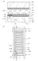
Images


Classifications
- G—PHYSICS
- G02—OPTICS
- G02F—OPTICAL DEVICES OR ARRANGEMENTS FOR THE CONTROL OF LIGHT BY MODIFICATION OF THE OPTICAL PROPERTIES OF THE MEDIA OF THE ELEMENTS INVOLVED THEREIN; NON-LINEAR OPTICS; FREQUENCY-CHANGING OF LIGHT; OPTICAL LOGIC ELEMENTS; OPTICAL ANALOGUE/DIGITAL CONVERTERS
- G02F1/00—Devices or arrangements for the control of the intensity, colour, phase, polarisation or direction of light arriving from an independent light source, e.g. switching, gating or modulating; Non-linear optics
- G02F1/01—Devices or arrangements for the control of the intensity, colour, phase, polarisation or direction of light arriving from an independent light source, e.g. switching, gating or modulating; Non-linear optics for the control of the intensity, phase, polarisation or colour
- G02F1/13—Devices or arrangements for the control of the intensity, colour, phase, polarisation or direction of light arriving from an independent light source, e.g. switching, gating or modulating; Non-linear optics for the control of the intensity, phase, polarisation or colour based on liquid crystals, e.g. single liquid crystal display cells
- G02F1/133—Constructional arrangements; Operation of liquid crystal cells; Circuit arrangements
- G02F1/1333—Constructional arrangements; Manufacturing methods
- G02F1/1343—Electrodes
- G—PHYSICS
- G02—OPTICS
- G02F—OPTICAL DEVICES OR ARRANGEMENTS FOR THE CONTROL OF LIGHT BY MODIFICATION OF THE OPTICAL PROPERTIES OF THE MEDIA OF THE ELEMENTS INVOLVED THEREIN; NON-LINEAR OPTICS; FREQUENCY-CHANGING OF LIGHT; OPTICAL LOGIC ELEMENTS; OPTICAL ANALOGUE/DIGITAL CONVERTERS
- G02F1/00—Devices or arrangements for the control of the intensity, colour, phase, polarisation or direction of light arriving from an independent light source, e.g. switching, gating or modulating; Non-linear optics
- G02F1/01—Devices or arrangements for the control of the intensity, colour, phase, polarisation or direction of light arriving from an independent light source, e.g. switching, gating or modulating; Non-linear optics for the control of the intensity, phase, polarisation or colour
- G02F1/13—Devices or arrangements for the control of the intensity, colour, phase, polarisation or direction of light arriving from an independent light source, e.g. switching, gating or modulating; Non-linear optics for the control of the intensity, phase, polarisation or colour based on liquid crystals, e.g. single liquid crystal display cells
- G02F1/133—Constructional arrangements; Operation of liquid crystal cells; Circuit arrangements
- G02F1/136—Liquid crystal cells structurally associated with a semi-conducting layer or substrate, e.g. cells forming part of an integrated circuit
- G02F1/1362—Active matrix addressed cells
- G02F1/136213—Storage capacitors associated with the pixel electrode
- G—PHYSICS
- G02—OPTICS
- G02F—OPTICAL DEVICES OR ARRANGEMENTS FOR THE CONTROL OF LIGHT BY MODIFICATION OF THE OPTICAL PROPERTIES OF THE MEDIA OF THE ELEMENTS INVOLVED THEREIN; NON-LINEAR OPTICS; FREQUENCY-CHANGING OF LIGHT; OPTICAL LOGIC ELEMENTS; OPTICAL ANALOGUE/DIGITAL CONVERTERS
- G02F1/00—Devices or arrangements for the control of the intensity, colour, phase, polarisation or direction of light arriving from an independent light source, e.g. switching, gating or modulating; Non-linear optics
- G02F1/01—Devices or arrangements for the control of the intensity, colour, phase, polarisation or direction of light arriving from an independent light source, e.g. switching, gating or modulating; Non-linear optics for the control of the intensity, phase, polarisation or colour
- G02F1/13—Devices or arrangements for the control of the intensity, colour, phase, polarisation or direction of light arriving from an independent light source, e.g. switching, gating or modulating; Non-linear optics for the control of the intensity, phase, polarisation or colour based on liquid crystals, e.g. single liquid crystal display cells
- G02F1/133—Constructional arrangements; Operation of liquid crystal cells; Circuit arrangements
- G02F1/1333—Constructional arrangements; Manufacturing methods
- G02F1/1343—Electrodes
- G02F1/134309—Electrodes characterised by their geometrical arrangement
- G02F1/134363—Electrodes characterised by their geometrical arrangement for applying an electric field parallel to the substrate, i.e. in-plane switching [IPS]
- G—PHYSICS
- G02—OPTICS
- G02F—OPTICAL DEVICES OR ARRANGEMENTS FOR THE CONTROL OF LIGHT BY MODIFICATION OF THE OPTICAL PROPERTIES OF THE MEDIA OF THE ELEMENTS INVOLVED THEREIN; NON-LINEAR OPTICS; FREQUENCY-CHANGING OF LIGHT; OPTICAL LOGIC ELEMENTS; OPTICAL ANALOGUE/DIGITAL CONVERTERS
- G02F2201/00—Constructional arrangements not provided for in groups G02F1/00 - G02F7/00
- G02F2201/40—Arrangements for improving the aperture ratio
Landscapes
- Physics & Mathematics (AREA)
- Nonlinear Science (AREA)
- Crystallography & Structural Chemistry (AREA)
- Mathematical Physics (AREA)
- Chemical & Material Sciences (AREA)
- General Physics & Mathematics (AREA)
- Optics & Photonics (AREA)
- Engineering & Computer Science (AREA)
- Geometry (AREA)
- Microelectronics & Electronic Packaging (AREA)
- Power Engineering (AREA)
- Liquid Crystal (AREA)
- Devices For Indicating Variable Information By Combining Individual Elements (AREA)
Description
Translated fromJapanese本発明は、液晶表示素子および表示装置に関し、特には、フリンジフィールドスイッチング(Fringe field switching(FFS))モード(別名;In Plane Switching(IPS)−Proモード)の液晶表示素子およびこれを備えた表示装置に関する。 The present invention relates to a liquid crystal display element and a display device, and in particular, a liquid crystal display element in a fringe field switching (FFS) mode (also known as In Plane Switching (IPS) -Pro mode) and a display including the same Relates to the device.
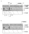
FFSモードの液晶表示装置は、液晶層に対して基板面に略平行な横電界を印加する共通電極と画素電極とが同一基板側に設けられており、この横電界によって液晶素子を駆動して画像表示を行う。ここで、従来のFFSモードの液晶表示装置について、図14を用いて説明する。ここで、図14(a)の平面図は、図14(b)のA-A’断面図を示している。 In the FFS mode liquid crystal display device, a common electrode and a pixel electrode for applying a lateral electric field substantially parallel to the substrate surface to the liquid crystal layer are provided on the same substrate side, and the liquid crystal element is driven by the lateral electric field. Display an image. Here, a conventional FFS mode liquid crystal display device will be described with reference to FIG. Here, the plan view of FIG. 14A is a cross-sectional view taken along the line A-A ′ of FIG.
この図に示す液晶表示装置は、透過型の液晶表示装置であり、液晶表示装置は、第1基板110と、この第1基板110の素子形成面側に対向配置された第2基板120と、これらの第1基板110と第2基板120との間に狭持された液晶層130とからなる液晶パネルを備えている。また、この液晶パネルにおいて、第1基板110および第2基板120の外側面には、偏光板140,150が密着状態で設けられており、第1基板110側の偏光板140のさらに外側には、透過表示を行うための光源となるバックライト(図示省略)が設けられている。 The liquid crystal display device shown in this figure is a transmissive liquid crystal display device, and the liquid crystal display device includes a
このうち第1基板110は、ガラス基板のような透明基板からなり、その液晶層130に向かう面上には、マトリクス状に配置された複数の走査線111および複数の信号線112を備えている。また、この走査線111と信号線112の各交差部には、各画素を駆動するための薄膜トランジスタ(Thin Film Transistor(TFT))1からなる駆動素子が設けられており、上記走査線111と信号線112で囲まれた領域が画素領域110Aとなる。 Among these, the
また、走査線111と隣接する画素の走査線111との間には、隣接する画素の走査線111側に、走査線111と平行に共通電位線113が設けられている。そして、同一面上の画素領域110Aにおいて、TFT1の形成領域を除く領域には、上記共通電位線113と一端側が重なる状態で、共通電極114が設けられている。この共通電極114は、走査線111と同一面で設けられるため、走査線111によりその配置が制限される。 Further, a common
また、上記TFT1のゲート電極2は、上記走査線111の一部で構成されており、上記走査線111、共通電位線113、共通電極114を覆う状態で、第1基板110上には、ゲート絶縁膜3が設けられている。さらに、ゲート電極2を覆うゲート絶縁膜3上には、半導体層4がパターン形成されている。 Further, the
上記半導体層4は、ゲート電極2の直上をチャネル層4aとし、その両側にn型不純物を含むソース領域4bとドレイン領域4cが設けられている。上記ソース領域4b上には、ソース領域4bと接続する状態でソース電極6aが配置され、このソース電極6aは上記信号線112と接続されている。また、ドレイン領域4c上には、ドレイン領域4cと接続する状態でドレイン電極6bが配置されている。以上のようにTFT1が構成される。 The
また、上記TFT1を覆う状態で、ゲート絶縁膜3上には、層間絶縁膜115が設けられている。この層間絶縁膜115には、TFT1のドレイン電極6bに達する状態のコンタクトホール115aが設けられており、層間絶縁膜115上には、このコンタクトホール115aを介してTFT1に接続された複数のスリット116aを有する画素電極116が設けられている。このスリット116aは、走査線111と平行に設けられている。また、上記画素電極116を覆う状態で、層間絶縁膜115上には、配向膜117が配置されている。 An interlayer
そして、スリット116aを挟んで設けられた画素電極116の電極部の端部と上記共通電極114との間に電界が生じることで、基板面に略平行な横電界が上記液晶層130に対して印加される。 Then, an electric field is generated between the end portion of the electrode portion of the
一方、第2基板120はガラス基板のような透明基板からなり、この第2基板120の液晶層130に向かう面には、R(赤)、G(緑)、B(青)各色のカラーフィルタ121と配向膜122がこの順に設けられている。 On the other hand, the
しかし、上述したような構成の液晶表示装置では、第1基板110の同一面上に走査線111と共通電極114とが配置されるため、走査線111により共通電極114の形成領域が制限される。よって、開口率が低く、透過率が低いという問題がある。However, in the liquid crystal display device having the above-described configuration, the
そこで、上記図を用いて説明した液晶表示装置の構成において、スリット116aを有する画素電極116をゲート絶縁膜3上に配置し、共通電極114を層間絶縁膜115上に配置した液晶表示装置の例が報告されている(例えば、特許文献1参照)。 Therefore, in the configuration of the liquid crystal display device described with reference to the above drawings, an example of a liquid crystal display device in which the
また、上記図を用いて説明した液晶表示装置の構成において、ゲート絶縁膜3上に共通電極114を配置した例も報告されている(例えば、特許文献2、3参照)。
しかし、特許文献1に記載された液晶表示装置では、共通電極114の配置制限はないものの、スリット116aを有する画素電極116が液晶層130側に配置されていないため、基板面に平行な電界がかかり難く、液晶層130を制御することが出来ず、液晶表示自体が難しい。 However, although the arrangement of the
また、特許文献2、3に記載された液晶表示装置では、信号線112により共通電極114の配置が制限されてしまい、開口率を広く取ることが難しい。 Further, in the liquid crystal display devices described in
そこで、開口率を向上させるために、図15(a)の平面図に示すように、信号線112側が共通電極114よりも一回り大きくなるように形成した画素電極116’を信号線112と重なる状態で配置することも考えられるが、図15(b)の回路図に示すように、信号線112と画素電極116’との間に寄生容量C1、C2が発生してしまい、縦クロストークの原因となってしまっていた。Therefore, in order to improve the aperture ratio, as shown in the plan view of FIG. 15A, a
そこで、本発明は、寄生容量を抑制した状態で開口率を向上させることが可能な液晶表示素子およびこれを備えた表示装置を提供することを目的とする。 Therefore, an object of the present invention is to provide a liquid crystal display element capable of improving the aperture ratio in a state where parasitic capacitance is suppressed and a display device including the liquid crystal display element.
本発明の液晶表示素子は、第1基板と第2基板との間に挟持された液晶層を備え、当該液晶層に対して電界を印加する共通電極と画素電極とを前記第1基板側に有し、第1基板上にマトリクス状に配置された複数の走査線および複数の信号線と、走査線および信号線の交差部に配置された駆動素子と、駆動素子を覆う状態で、第1基板上に設けられた第1絶縁膜と、第1絶縁膜上に配置された共通電極と、共通電極を覆う状態で、第1絶縁膜上に配置された第2絶縁膜と、画素領域内に配置され、前記第2絶縁膜および前記第1絶縁膜に設けられたコンタクトホールを介して前記駆動素子と接続された複数のスリットを有する画素電極とを備え、共通電極は、第1絶縁膜上のコンタクトホールの形成領域を除く画素領域と、駆動素子のゲート電極を含む走査線と、信号線とを覆う状態で配置され、画素電極の複数のスリットは、信号線と平行に設けられ、画素電極は、当該画素電極の信号線側の端部と当該信号線に最も近い位置のスリットとの間の電極部の幅が、他のスリット間の電極部の幅よりも狭くなるように構成されていることを特徴としている。The liquid crystal display element of the present invention includes a liquid crystal layer sandwiched between a first substrate and a second substrate, and a common electrode and a pixel electrode for applying an electric field to the liquid crystal layer are disposed on the first substrate side. A plurality of scanning lines and a plurality of signal lines arranged in a matrix on the first substrate; a driving element arranged at an intersection of the scanning lines and the signal line; A first insulating film provided on the substrate; a common electrode disposed on the first insulating film; a second insulating film disposed on the first insulating film in a state of covering the common electrode; and a pixel region And a pixel electrode having a plurality of slits connected to the driving element via a contact hole provided in the second insulating film and the first insulating film, and the common electrode is a first insulating film Pixel area excluding contact hole formation area above and gate of drive element A scanning line including the poles, are arranged in the state of covering the signalline, a plurality of slits of the pixel electrode is provided parallel to the signal lines, pixel electrodes, the end and the signal on the signal line side of the pixel electrode The electrode portion between the slits closest to the line is configured to be narrower than the width of the electrode portion between the other slits .
本発明の表示装置は、第1基板と第2基板との間に挟持された液晶層を備え、当該液晶層に対して電界を印加する共通電極と画素電極とを第1基板側に有する液晶表示素子を有しており、この液晶表示素子によって変調された光を用いて映像表示を行う表示装置において、第1基板上にマトリクス状に配置された複数の走査線および複数の信号線と、走査線および信号線の交差部に配置された駆動素子と、駆動素子を覆う状態で、第1基板上に設けられた第1絶縁膜と、第1絶縁膜上に配置された共通電極と、共通電極を覆う状態で、第1絶縁膜上に配置された第2絶縁膜と、画素領域内の前記第2絶縁膜上に配置され、前記第2絶縁膜および前記第1絶縁膜に設けられたコンタクトホールを介して前記駆動素子と接続された複数のスリットを有する画素電極とを備え、共通電極は、第1絶縁膜上のコンタクトホールの形成領域を除く画素領域と、駆動素子のゲート電極を含む走査線と、信号線とを覆う状態で配置され、画素電極の複数のスリットは、信号線と平行に設けられ、画素電極は、当該画素電極の信号線側の端部と当該信号線に最も近い位置のスリットとの間の電極部の幅が、他のスリット間の電極部の幅よりも狭くなるように構成されていることを特徴としている。The display device of the present invention includes a liquid crystal layer sandwiched between a first substrate and a second substrate, and a liquid crystal layer having a common electrode and a pixel electrode for applying an electric field to the liquid crystal layer on the first substrate side. In a display device having a display element and displaying an image using light modulated by the liquid crystal display element, a plurality of scanning lines and a plurality of signal lines arranged in a matrix on the first substrate; A driving element disposed at an intersection of the scanning line and the signal line; a first insulating film provided on the first substrate in a state of covering the driving element; a common electrode disposed on the first insulating film; A second insulating film disposed on the first insulating film in a state of covering the common electrode, and disposed on the second insulating film in the pixel region, and provided on the second insulating film and the first insulating film. A plurality of slits connected to the driving element through contact holes And a pixel electrode having a common electrode, a pixel region excluding the formation region of the contact hole on the first insulating film, and a scanning line including a gate electrode of the drive element are arranged in the state of covering the signalline, the pixel The plurality of slits of the electrode are provided in parallel with the signal line, and the pixel electrode has a width of the electrode portion between the end of the pixel electrode on the signal line side and the slit closest to the signal line, and the like. It is characterizedby being comprised so that it maybecome narrower than the width | variety of the electrode part between these slits .
このような液晶表示素子および表示装置によれば、信号線および走査線を覆う第1絶縁膜上に、上記コンタクトホールの形成領域を除く画素領域だけでなく、走査線および信号線の少なくとも一方を覆う状態で、上記共通電極が配置されることから、有効画素領域が増大し、開口率を向上させることが可能となる。また、共通電極が走査線および信号線の少なくとも一方を覆う状態で配置されることで、走査線と画素電極の間または信号線と画素電極の間の寄生容量が抑制される。 According to such a liquid crystal display element and display device, not only the pixel region except the contact hole formation region but also at least one of the scan line and the signal line is formed on the first insulating film covering the signal line and the scan line. Since the common electrode is disposed in a covered state, the effective pixel area is increased and the aperture ratio can be improved. In addition, since the common electrode is arranged in a state of covering at least one of the scanning line and the signal line, parasitic capacitance between the scanning line and the pixel electrode or between the signal line and the pixel electrode is suppressed.
以上説明したように、本発明の液晶表示素子および表示装置によれば、開口率を向上させることができるため、光透過率が向上し、液晶表示装置のコントラストを向上させることができる。また、走査線と画素電極の間または信号線と画素電極の間の寄生容量を抑制されることで、画素内の信号ノイズを防止することができるため、保持された画素電位が安定し、縦、横クローストークが発生しないことから、液晶表示装置の高画質化が図れる。 As described above, according to the liquid crystal display element and the display device of the present invention, since the aperture ratio can be improved, the light transmittance can be improved and the contrast of the liquid crystal display device can be improved. In addition, by suppressing the parasitic capacitance between the scan line and the pixel electrode or between the signal line and the pixel electrode, signal noise in the pixel can be prevented, so that the held pixel potential is stabilized and the vertical Since no horizontal crosstalk occurs, the image quality of the liquid crystal display device can be improved.
また、本実施形態の液晶表示素子およびこれを備えた表示装置は、例えばトランジスタからなる駆動素子に対して、信号線、走査線、画素電極からの電界で半導体層にバックチャンネルを発生させないため、寄生バックチャンネルによる不安定な動作が防止される。 In addition, the liquid crystal display element of the present embodiment and the display device including the same do not generate a back channel in the semiconductor layer due to the electric field from the signal line, the scanning line, and the pixel electrode, for example, with respect to the driving element including a transistor. Unstable operation due to the parasitic back channel is prevented.
以下、本発明の実施の形態について詳細に説明する。 Hereinafter, embodiments of the present invention will be described in detail.
(第1実施形態)
図1(a)は、FFSモードの透過型の液晶表示装置の断面図であり、図1(b)は平面図である。なお、図1(a)は図1(b)のA-A’断面を示す。(First embodiment)
FIG. 1A is a cross-sectional view of an FFS mode transmissive liquid crystal display device, and FIG. 1B is a plan view. FIG. 1A shows a cross section taken along the line AA ′ of FIG.
すなわち液晶表示装置100は、第1基板10と、この第1基板10の素子形成面側に対向配置された第2基板20と、これらの第1基板10と第2基板20との間に狭持された液晶層30とからなる液晶パネルを備えている。ここでは、液晶層30が、ネマチック液晶で構成されていることとする。またこの液晶パネルにおいて、第1基板10および第2基板20の外側面には、偏光板40,50が接着剤(図示省略)を介して密着状態で設けられている。これらの偏光板40,50は、クロスニコル状態で設けられていることとする。また、第1基板10側の偏光板40のさらに外側には、透過表示を行うための光源となるバックライト(図示省略)が設けられている。 That is, the liquid crystal display device 100 is narrowed between the
上記構成のうち、第1基板10を除く構成は一般的な構成であり、例えば表示側基板となる第2基板20はガラス基板のような透明基板からなり、この第2基板20の液晶層30に向かう面には、R(赤)、G(緑)、B(青)各色のカラーフィルタ21と配向膜22とがこの順に設けられている。 Among the above-described configurations, the configuration excluding the
一方、背面側基板となる第1基板10については、本発明に特徴的な構成を有するため、以下に詳細に説明する。 On the other hand, the
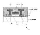
上記第1基板10は、ガラス基板のような透明基板からなり、その液晶層30に向かう面上には、マトリクス状に配置された複数の走査線11および複数の信号線12を備えている。走査線11および信号線12の構成材料としては、アルミニウム(Al)、モリブデン(Mo)、クロム(Cr)、タングステン(W)、チタン(Ti)、鉛(Pb)、またはこれらの複合層(etc,Ti/Al)もしくは金属化合物層(MoSi,AlSi)が用いられ、ここでは、例えばどちらもアルミニウム(Al)で構成されることとする。ただし、走査線11と信号線12は異なる材料で構成されてもよい。 The
また、この走査線11と信号線12の各交差部には、各画素を駆動するための例えばボトムゲート型のTFT1からなる駆動素子が設けられており、上記走査線11と信号線12で囲まれた領域が画素領域1Aとなる。ここで、この画素領域1Aは、例えば信号線12側を長辺、走査線11側を短辺とする平面視矩形状であることとする。 Further, at each intersection of the
ここで、図2(a)のA−A’断面の要部拡大図に示すように、走査線11の一部で上記TFT1のゲート電極2が構成されており、上記ゲート電極2を含む走査線11を覆う状態で、上記第1基板10上に、ゲート絶縁膜3が設けられている。また、ゲート電極2を覆うゲート絶縁膜3上には、半導体層4がパターン形成されている。 Here, as shown in the enlarged view of the main part of the AA ′ cross section of FIG. 2A, the
ここで、半導体層4は、例えばアモルファスシリコン(a−Si)、ポリシリコン(Poly−Si)または単結晶シリコンで構成されており、ゲート電極2の直上をチャネル層4aとし、その両側に例えばn型不純物を含むソース領域4bとドレイン領域4cが設けられている。また、チャネル層4aとソース・ドレイン領域4b、4cとの間には、ソース・ドレイン領域4b、4cよりも不純物濃度の低いLDD領域4b’、4c’がそれぞれ設けられている。 Here, the
また、上記半導体層4を覆う状態で、ゲート絶縁膜3上には、絶縁層5が設けられており、この絶縁層5に上記ソース・ドレイン領域4b、4cに達する状態で設けられたコンタクトホールを介して、上記ソース・ドレイン領域4b、4cにソース電極6aとドレイン電極6bが接続されている。なお、このソース電極6aは上記信号線12と同一層で接続されている。 In addition, an insulating
そして、上記ソース・ドレイン電極6a、6bを覆う状態で、絶縁層5上に、第1絶縁膜13が設けられている。ここで、この第1絶縁膜13は、後工程で、第1絶縁膜13上に形成する第2絶縁膜を200℃〜400℃程度の高温で成膜するため、耐熱性を有するだけでなく、その上層に共通電極を形成することから平坦性を有することが好ましい。また、寄生容量を抑制するため、比誘電率が低く、透過率が高く、膜応力が低い膜であることが好ましい。このような特性を有する第1絶縁膜13としては、例えばSOG(Spin On Glass)膜が特に好適に用いられる。ここで、第1絶縁膜13の膜厚は、走査線11、信号線12、後工程で第1絶縁膜13上に形成する共通電極の負荷容量に大きく影響し、膜厚が厚いほど負荷容量は低減される。このため、第1絶縁膜13の膜厚は、液晶表示素子の駆動特性の許容範囲内で、例えば0.5μm〜4.0μm程度の膜厚で形成されることが好ましい。 A first insulating
なお、第1絶縁膜13としては、上記SOG膜の他に、化学的気相成長(Chemical Vapor Deposition(CVD))法により成膜された酸化シリコン(SiO2)や窒化シリコン(SiN)等の無機絶縁膜を用いてもよく、有機絶縁膜を用いてもよい。ただし、第1絶縁膜13としては、CVD法により成膜した無機絶縁膜を用いるよりも有機絶縁膜を用いた方が、平坦性を有し、比誘電率が低く、塗布法により容易に成膜できるため、好ましい。有機絶縁膜としては、非感光性樹脂と感光性樹脂とが用いられ、非感光性樹脂としては、例えばアクリル樹脂、ポリエステル、塩化ビニル、ポリカーボネート、ポリプロピレン、ポリエチレン、トリアセテート、ポリイミド等、感光性樹脂としては、例えばアクリル樹脂、ポリイミド、住友ベークライト社製スミレジンエクセルCRC−8300等が挙げられる。ここで、有機絶縁膜材料の物性を表1に示す。
そして、本発明の特徴的な構成として、後述する画素電極と上記TFT1とを接続するためのコンタクトホールの形成領域を除く画素領域1Aと、上記走査線11上および上記信号線12上の少なくとも一方とを覆う状態で、上記第1絶縁膜13上に共通電極14が設けられている。これにより、上記走査線11上および上記信号線12上の少なくとも一方が共通電極14で覆われる分、有効画素領域が増大し、開口率を向上させることが可能となる。この共通電極14は、例えばITO(IndiumTin Oxide)、IZO(Indium Zinc Oxide)等の透明電極膜で形成される。As a characteristic configuration of the present invention, a
ここでは、上記コンタクトホールの形成領域を除く表示領域の全域に共通電極14が設けられることとする。この場合には、表示領域外でVcom端子に接続された金属配線から共通電極14に電位が供給されるため、さらに開口率を向上させることが可能となる。ここで、コンタクトホールと共通電極14とは、後述するように、コンタクトホール内に配置される画素電極と共通電極とがショートしない程度に離間していればよい。 Here, it is assumed that the
なお、本実施形態では、表示領域外でVcom端子に接続された金属配線から共通電極14に電位が供給されることとしたが、図2(b)に示すように、共通電極14と接続する状態で、第1絶縁膜13上に、共通電極14よりも抵抗値の低い材料からなる複数の共通電位線18が、走査線11と平行に配置されていてもよい。この共通電位線18は、例えばAl、Mo、Ti、Pb、W、Cr、またはこれらの複合層(etc,Ti/Al)、もしくは金属化合物層(MoSi,AlSi)で形成される。ここでは、共通電位線18が例えば走査線11および信号線12と同じAlで構成されることとするが、上記走査線11、信号線12と共通電位線18が異なる材料で構成されていてもよい。 In the present embodiment, the potential is supplied to the
ここで、図3に共通電位線が配置されていない場合(a)と共通電位線が配置された場合(b)について、抵抗値の違いを比較するための模式図を示す。なお、ここでは、Vcom端子Vに接続された金属配線19が、画素領域1Aを配列してなる表示領域10Aの両側に表示領域10Aを挟んで並設され、これらの金属配線19からコンタクトホールを除く表示領域10Aの全域に設けられた共通電極14に電位が供給されることとする。これにより、2本の金属配線19から表示領域10Aの中心部Oに向けて電位が供給される。 Here, FIG. 3 shows a schematic diagram for comparing the difference in resistance value when the common potential line is not arranged (a) and when the common potential line is arranged (b). Here, the
ここで、図3(a)に示すように、共通電位線が配置されておらず、表示領域10A外に配置された金属配線19からITOからなる共通電極14に直接電位が供給される場合には、ITOの抵抗が10〜200Ω/□であるため、表示領域10Aの端部から中心部Oまでの共通電極14の抵抗R1が大きくなってしまい。このため、表示領域10Aの端部から中心部Oまでの供給電位に時間的なずれが生じ、液晶パネルの表示領域10Aにおける場所による輝度差が生じてしまう。これに対し、図3(b)に示すように、複数の共通電位線18を画素列毎に配置すると、共通電位線18を構成する金属材料は、例えばAlが0.05Ω/□、Moが0.5Ω/□と、共通電極14を構成するITOよりも抵抗が低いため、表示領域10Aの端部から中心部Oまでの共通電極14の抵抗R2は、上記R1よりも小さくなる。これにより、表示領域10Aの端部から中心部Oまでの供給電位の時間的なずれが防止され、表示領域10Aの場所による輝度差を改善することが可能となる。Here, as shown in FIG. 3A, when the common potential line is not arranged and the potential is directly supplied from the
また、この共通電位線18を、走査線11または信号線12と重なる状態で配置することで、開口率に影響を与えずに共通電位線18を配置することができるため、好ましい。 In addition, it is preferable to dispose the common
なお、ここでは、2本の金属配線19が表示領域10Aの両側に配置された例について説明したが、1本の金属配線19が表示領域10Aの片側のみに配置されてもよい。ただし、2本の金属配線19が表示領域10Aの両側に配置された方が、表示領域10Aの端部から中心部までの共通電極14の抵抗を低くすることができるため、好ましい。 Here, an example in which two
また、ここでは、共通電位線18を第1絶縁膜13と共通電極14との間に配置したが、共通電位線18は、共通電極14と接続すればよく、絶縁層5上、ゲート絶縁膜3上、第1基板10上のいずれに配置してもよい。 Here, the common
ここで、再び図2(a)に示すように、共通電極14上には、例えばCVD法により成膜されたSiO2、SiN等の無機絶縁膜からなる第2絶縁膜15が設けられている。この第2絶縁膜15をCVD法により成膜された無機絶縁膜とすることで、焼き付き防止や歩留まり向上等の利点がある。なお、第2絶縁膜15としては、上記以外にも、SOG、有機絶縁膜を用いることが可能である。有機絶縁膜としては、第1絶縁膜13で例示した材料と同一のものを用いることができる。Here, as shown in FIG. 2A again, a second insulating
ここで、第1絶縁膜13と第2絶縁膜15の組み合わせを、表2に示す。
この表に示すように、第1絶縁膜13と第2絶縁膜15としては、様々な組み合わせが考えられるが、上述したように、第1絶縁膜13としては、SOG、有機絶縁膜、また、第2絶縁膜15としては、CVD法により成膜された無機絶縁膜(表中、CVD−無機絶縁膜)を用いた方式1、2の組み合わせが好ましい。 As shown in this table, various combinations are conceivable as the first insulating
上記第2絶縁膜15および第1絶縁膜13には、上記ドレイン電極6bに達するコンタクトホール15a、13aが連通する状態で、すなわち平面視的に重なる状態で設けられている。そして、このコンタクトホール15a、13aを介して上記ドレイン電極6bと接続された状態で、上記第2絶縁膜15上に、画素電極16が設けられている。 The second insulating
ここで、上記コンタクトホール15a、13aは平面視的に重なる状態で配置されるため、同一のエッチングマスクを用いた一度のエッチングにより形成することが好ましい。また、コンタクトホール15a、13aが平面視的に重ならない場合についても本発明は適用可能であるが、重なる方が開口率を広くとることができるため、好ましい。 Here, since the
また、画素電極16を覆う状態で、第2絶縁膜15上には、配向膜17が配置されている。ここで、図1(b)に示すように、この画素電極16は複数のスリット16aを有しており、このスリット16aは、信号線12と平行に設けられている。 An
上記画素電極16の複数のスリット16aが信号線12と平行に配置されることで、背景技術で図14を用いて説明したように、複数のスリットが走査線11と平行に配置される場合と比較して、有効画素領域が増大する。これは、上記スリットが走査線11と平行である場合には、信号線12に近いスリットの短辺側は、この短辺を構成する電極部により液晶分子mの配向が阻害されるため有効画素領域とならないが、上記スリット16aが信号線12と平行に配置されることで、画素電極16の信号線12の端部側まで有効画素領域とすることができる。また、この場合でも画素電極16のスリット16aの短辺側は有効画素領域とはならないが、この部分を走査線11と重ねることで、開口率を広くとることが可能となるため、好ましい。 Since the plurality of
ここで、図1(b)のB−B’断面である図4に示すように、各画素を駆動させるための駆動電圧は、画素電極16の中央部のスリット16aの幅と、スリット16a間の電極部16bの幅と第2絶縁膜15の膜厚とで規定され、隣接する画素の画素電極16間の間隔Xは、近すぎると隣接する画素からの光漏れが生じるため、所定の間隔以上離して配置することが好ましい。そこで、画素電極16の信号線12側の端部と信号線12に最も近い位置のスリット16aとの間の電極部16b’の幅を、この電極部16b’以外の電極部16bと異なる幅に調整することで、隣接する画素の画素電極16間の間隔Xを制御する。 Here, as shown in FIG. 4 which is a BB ′ cross section of FIG. 1B, the driving voltage for driving each pixel is the width of the
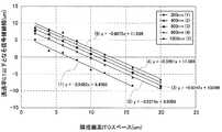
ここで、図5に、隣接する黒表示状態の画素Aと白表示状態の画素Bの画素電極16間の間隔Xを、2、4、6、7、8、10、12、16、20μmと変えた場合に、画素Bから画素Aへの光漏れを、縦軸を透過率として測定したグラフを示す。このグラフに示すように、隣接画素の画素電極16間の間隔Xが小さくなるほど、光漏れが発生することが確認された。ここで、Alからなる信号線12は、遮光体として機能するため、信号線12の線幅Zを大きくすることで、光漏れを防ぐことが可能となる。Here, in FIG. 5, the distance X between the
そこで、光漏れが視認されない程度の黒表示画素Aでの透過率0.1以下をクライテリアとし、隣接画素の画素電極16間の間隔Xを横軸にとり、第2絶縁膜15の膜厚Yを200、400、600、800、1000nmとした場合に、黒表示画素Aの透過率が0.1以下となる信号線12の線幅Zをシミュレーションしたグラフを図6に示す。このグラフに示すように、上記信号線幅Z(y)は、画素電極16間の間隔X(x)を変数とした一次関数で示され、傾きは第2絶縁膜15の膜厚によらず、ほぼ一定であることが確認された。また、y切片は第2絶縁膜15の膜厚依存性があり、第2絶縁膜15の膜厚が厚いほど、遮光体となる信号線の線幅を広くとる必要があることが確認された。Therefore, the criterion is a transmittance of 0.1 or less in the black display pixel A where light leakage is not visually recognized, the interval X between the
そこで、傾きは第2絶縁膜15の膜厚Yを変えた場合の5つの式の平均値とし、切片については近似式を用いて式を一般化した。ここで、図7(a)は対数近似、図7(b)は線形近似のグラフを示す。 Therefore, the slope is an average value of five formulas when the film thickness Y of the second insulating
そして、上記式から必要な信号線12の線幅Zは、対数近似を用いた場合は下記数式(1)で表され、線形近似を用いた場合には下記数式(2)で表される。
上記の2式のどちらかが成り立つように隣接画素の画素電極間の間隔X、第2層間絶縁膜の膜厚Y、遮光物の線幅Zを設定する。特に精度の高い対数近似の数式(1)により、各値を設定すると、光漏れを確実に抑制することが可能となる。 The interval X between the pixel electrodes of adjacent pixels, the film thickness Y of the second interlayer insulating film, and the line width Z of the light shield are set so that either of the above two formulas holds. In particular, when each value is set according to the mathematically approximated logarithmic approximation (1), light leakage can be reliably suppressed.
ただし、本実施形態においては、信号線12が遮光体を兼ねており、信号線12の線幅Zおよび第2絶縁膜15の膜厚Yは液晶表示素子の設計上で規定される。ただし、線幅Zが小さい方が、開口率が高くなるため、Zを最低値とし、隣接画素の画素電極間の間隔Xを上記数式(1)または数式(2)を満たすように設定する。そして、図8に示すように、信号線12に最も近い画素電極16の電極部16b’の幅を他の電極部16bの幅よりも狭くすることで、隣接画素の画素電極間の間隔Xを調整する。 However, in the present embodiment, the
なお、本実施形態では、信号線12が遮光体として機能することとしたが、信号線12の下層に、どの電極とも電気的に接続されていない遮光体を配置してもよい。 In the present embodiment, the
次に、上記液晶表示装置100の動作について、再び図1を用いて説明する。無電界時においては、液晶層30中の液晶分子mが位相差を生じないように配向されるため、偏光板40を通過したバックライトの光hが、偏光板40に対してクロスニコル状態で配置された偏光板50で吸収され、黒表示となる。 Next, the operation of the liquid crystal display device 100 will be described with reference to FIG. 1 again. When there is no electric field, the liquid crystal molecules m in the
一方、電界印加時においては、液晶層30を透過することでλ/2の位相差を生じるように液晶分子mが配向する。これにより、偏光板40を通過したバックライトの光hが、液晶層30を透過することで、λ/2の位相差を生じて90°回転した直線偏光となるため、偏光板50を透過し、白表示となる。 On the other hand, when an electric field is applied, the liquid crystal molecules m are aligned so as to cause a phase difference of λ / 2 by passing through the
次いで、この液晶表示装置100の回路図を図9に示す。この液晶表示装置100の第1基板10上には、表示領域10Aとその周辺領域10Bとが設定されている。ただし、この場合の回路図は図3(a)、(b)を用いて説明したように、電位を供給する金属配線19が表示領域10A外の一方の周辺領域10Bのみに配置された場合の回路図である。 Next, a circuit diagram of the liquid crystal display device 100 is shown in FIG. On the
上記表示領域10Aは、複数の走査線11と複数の信号線12とがマトリクス状に配線されており、それぞれの交差部に対応して1つの画素Aが設けられた画素アレイ部として構成されている。 The
また、上記周辺領域10Bには、表示領域10Aの各画素Aを行単位で順次選択する垂直ドライバ61、行単位で選択された各画素Aに画素信号を書き込む水平ドライバ62、時分割駆動のための時分割スイッチ部63および垂直、水平ドライバ61,62や時分割スイッチ部63をコントロールする制御系64が実装された構成となっている。 Further, in the
画素Aの各々は、ゲート電極が走査線11-1〜11-mに接続され、ソース電極6aが信号線12-1〜12-nに接続されたTFT1と、このTFT1のドレイン電極6bに画素電極16が接続された表示素子Dと、TFT1のドレイン電極6bに一方の電極が接続された補助容量Sとから構成されている。かかる構成の画素Aの各々において、表示素子Dの共通電極は、補助容量Sの他方の電極と共に共通電位線18に接続されている。共通電位線18には、所定の直流電圧もしくは水平同期信号と同期した矩形電圧が共通電位電圧VCOMとして与えられる。 Each of the pixels A includes a
ここで、この液晶表示装置100は、時分割駆動法により駆動される。時分割駆動法とは、表示領域10Aの互いに隣り合う複数本の信号線12を1単位(ブロック)として分割し、この1分割ブロック内の複数本の信号線12に与える信号電圧を時系列で水平ドライバ62の各出力端子から出力する一方、複数本の信号線12を1単位として時分割スイッチ部63を設け、この時分割スイッチ部63によって水平ドライバ62から出力される時系列の信号電圧を時分割でサンプリングして複数本の信号ラインに順次与える駆動方法である。 Here, the liquid crystal display device 100 is driven by a time division driving method. In the time division driving method, a plurality of
上記時分割スイッチ部63は、水平ドライバ62から出力される時系列の信号電圧を時分割でサンプリングするアナログスイッチ(トランスミッションスイッチ)によって構成されている。この時分割スイッチ部63の具体的な構成例を示す。なお、この時分割スイッチ部63は、水平ドライバ62の各出力に対して1個ずつ設けられるものである。また、ここでは、R(赤),G(緑),B(青)に対応して3時分割駆動を行う場合を例にとって示している。 The time
この時分割スイッチ部63は、PchMOSトランジスタおよびNchMOSトランジスタが並列に接続されてなるCMOS構成のアナログスイッチ63-1,63-2,63-3によって構成されている。なお、本例では、アナログスイッチ63-1,63-2,63-3として、CMOS構成のものを用いるとしたが、PMOSあるいはNMOS構成のものを用いることも可能である。 The time
この時分割スイッチ部63において、3個のアナログスイッチ63-1,63-2,63-3の各入力端が共通に接続され、各出力端が3本の信号ライン12-1,12-2,12-3の各一端にそれぞれ接続されている。そして、これらアナログスイッチ63-1,63-2,63-3の各入力端には、水平ドライバ62から時系列で出力される信号電位が与えられる。In this time
ここで、本発明における共通電極14をアナログスイッチ63-1,63-2,63-3の上部にも配置することにより、ボトムゲート構造のTFT1により形成されたアナログスイッチ63-1,63-2,63-3は、近傍のゲート選択信号、隣接の信号線12−1,12−2,12−3各々からの寄生容量による電位変動の影響を削除することができる。なお、これは、アナログスイッチ63-1,63-2,63-3がトップゲート構造で形成された場合に関しても同様な効果をもつのは明らかである。Here, by arranging the
また、1個のアナログスイッチにつき2本ずつ、合計6本の制御ライン65-1〜65-6が配線されている。そして、アナログスイッチ63-1の2つ制御入力端(即ち、CMOSトランジスタの各ゲート)が制御ライン65-1,65-2に、アナログスイッチ63-2の2つ制御入力端が制御ライン65-3,65-4に、アナログスイッチ63-3の2つ制御入力端が制御ライン65-5,65-6にそれぞれ接続されている。 Also, a total of six control lines 65-1 to 65-6 are wired, two for each analog switch. Two control input terminals (that is, gates of the CMOS transistors) of the analog switch 63-1 are connected to the control lines 65-1 and 65-2, and two control input terminals of the analog switch 63-2 are connected to the control line 65-. Two control input terminals of the analog switch 63-3 are connected to the control lines 65-5 and 65-6, respectively.
6本の制御ライン65-1〜65-6に対して、3個のアナログスイッチ63-1,63-2,63-3を順に選択するためのゲート選択信号S1〜S3,XS1〜XS3が、後述するタイミングコントローラ(TC)66から与えられる。ただし、ゲート選択信号XS1〜XS3は、ゲート選択信号S1〜S3の反転信号である。 For the six control lines 65-1 to 65-6, gate selection signals S1 to S3 and XS1 to XS3 for sequentially selecting the three analog switches 63-1 63-2, and 63-3 are provided. It is given from a timing controller (TC) 66 described later. However, the gate selection signals XS1 to XS3 are inverted signals of the gate selection signals S1 to S3.
ゲート選択信号S1〜S3,XS1〜XS3は、水平ドライバ62から出力される時系列の信号電位に同期して、3個のアナログスイッチ63-1,63-2,63-3を順次オンさせる。これにより、アナログスイッチ63-1,63-2,63-3は、水平ドライバ62から出力される時系列の信号電位を、1H期間に3時分割でサンプリングしつつ、対応する信号ライン12-1,12-2,12-3にそれぞれ供給する。 The gate selection signals S1 to S3 and XS1 to XS3 sequentially turn on the three analog switches 63-1, 63-2, 63-3 in synchronization with the time-series signal potential output from the
垂直ドライバ61、水平ドライバ62および時分割スイッチ部63を制御する制御系64は、タイミングコントローラ(TC)66、基準電圧発生源67およびDC-DCコンバータ68などを有し、これら回路が上記第1基板の周辺領域10B上に垂直ドライバ61、水平ドライバ62および時分割スイッチ部63と共に実装された構成となっている。 A
この制御系64において、タイミングコントローラ66には、例えば、外部の電源部(図示せず)から電源電圧VDDが、外部のCPU(図示省略)からデジタル画像データdataが、外部のクロック発生器(図示省略)からクロックCLKがそれぞれTCP(図示省略)を通して入力される。 In the
ここで、本実施形態の液晶表示装置の各画素Aの回路図を図10に示すと、共通電極14がコンタクトホール形成領域を除く表示領域10Aの全域に設けられることで、信号線12と画素電極16との間および走査線11と画素電極16との間に発生する寄生容量C1、C2が共通電極14に結合し、画素電位への影響が抑制される。 Here, when the circuit diagram of each pixel A of the liquid crystal display device of the present embodiment is shown in FIG. 10, the
このような液晶表示素子およびこれを備えた表示装置によれば、上記共通電極14が、第1絶縁膜13上に、コンタクトホール13a、15aの形成領域を除く画素領域1Aだけでなく、走査線11および信号線12の少なくとも一方を覆う状態で配置されることから、有効画素領域を増大させることが可能となり、開口率を向上させることが可能となる。したがって、光透過率が向上し、コントラストを向上させることができる。 According to such a liquid crystal display element and a display device including the same, the
また、共通電極14が走査線11および信号線12の少なくとも一方を覆う状態で配置されることで、信号線12と画素電極16の間または走査線11と画素電極16の間の寄生容量が抑制される。特に、本実施形態の液晶表示装置によれば、コンタクトホール13a、15aの形成領域以外の表示領域10Aの全域が共通電極14で覆われている。これにより、画素内の信号ノイズを確実に防止することができるため、保持された画素電位が安定し、縦、横クローストークが発生しないことから、液晶表示装置の高画質化が図れる。 In addition, since the
また、本実施形態の液晶表示素子およびこれを備えた表示装置は、a−Si、poly−Si、またはcrystal−Siを半導体層4として使用するボトムゲート型のTFT1に対して、信号線11、走査線12、画素電極16からの電界で半導体層にバックチャンネルを発生させないため、寄生バックチャンネルによる不安定な動作がない。これは、トップゲートTFTに関しても同様な効果をもつのは明らかである。 In addition, the liquid crystal display element of this embodiment and the display device including the liquid crystal display element include a
なお、TFT1がトップゲート型のトランジスタである場合には、図11に示すように、第1基板10上に、a−Si、Poly−Siまたはcrystal−Siからなる半導体層4がパターン形成され、この半導体層4上にゲート絶縁膜3を介して一部がゲート電極2として機能する一方向に延設された走査線11がパターン形成される。この場合には、ゲート電極2をマスクとしてn型不純物がイオン注入されるため、ゲート電極2直下の半導体層4がチャネル層4aとなり、その両側の半導体層4がソース領域4bとドレイン領域4cになる。また、ゲート電極2およびゲート絶縁膜3上には、絶縁層5が設けられており、絶縁層5に設けられたコンタクトホール5a、5bを介して、ソース・ドレイン領域4b,4cとソース・ドレイン電極6a,6bが接続される。そして、ソース・ドレイン電極6a,6bを覆う状態で第1絶縁膜13が設けられている。In the case where the
(変形例1)
なお、上述した第1実施形態では、画素電極16が矩形状であり、矩形状のスリット16aが設けられた例について説明したが、図12の平面図に示すように、画素電極16’が平面視的にその長手方向の中央部で曲折した形状、すなわち「くの字状(V字状)」に曲折した形状のマルチドメイン構造であってもよい。この場合には、画素電極16’のスリット16a’も画素電極16’の外形状に合わせて「くの字状(V字状)」に開口される。画素領域1A内で、電界方向が異なる2つの領域が存在するため、液晶分子mの配向方向2方向となり、視野角特性を大幅に改善することができる。この場合には、信号線12も上記画素電極16’の曲折に合わせてジグザグ状に配置される。(Modification 1)
In the first embodiment described above, an example in which the
ここで、「くの字状(V字状)」に開口されるスリット16a’は、上述した電界方向が異なる2つの領域において、電界印加時の上記液晶分子mの長軸の配向方向を90°とした場合に、上記液晶分子mの長軸に対するスリット16a’の長手方向の角度の範囲が45°以上90°未満、好ましくは65°以上89°以下となるようにする。 Here, the
(変形例2)
また、図13の平面図に示すように、画素電極16”の複数のスリット16a”は、走査線11と略平行に配置されていてもよい。ここで、略平行とは、走査線11に対して0°から45°程度までの傾きを有することを指す。この場合であっても、共通電極14がコンタクトホール13a、15aの形成領域を除く表示領域10Aの全域に配置されることで、開口率が向上し、信号線12と画素電極16”、走査線11と画素電極16”の寄生容量が抑制される。ただし、開口率は、第1実施形態で説明したように、画素電極16のスリット16aを信号線12と平行に配置した方が、広くなるため、好ましい。(Modification 2)
Further, as shown in the plan view of FIG. 13, the"plurality of
このような液晶表示装置であっても、開口率が広くなることで、光透過率が向上し、コントラストを向上させることができる。また、走査線と画素電極の間または信号線と画素電極の間の寄生容量が抑制されることで、画素内の信号ノイズを防止することができるため、保持された画素電位が安定し、縦、横クローストークが発生しないことから、液晶表示装置の高画質化が図れる。 Even in such a liquid crystal display device, since the aperture ratio is widened, the light transmittance can be improved and the contrast can be improved. In addition, since the parasitic capacitance between the scan line and the pixel electrode or between the signal line and the pixel electrode is suppressed, signal noise in the pixel can be prevented. Since no horizontal crosstalk occurs, the image quality of the liquid crystal display device can be improved.
なお、この変形例2の構成においても、図2(b)を用いて説明したように、上記共通電極14と接続される共通電位線を配置してもよく、上記変形例1で説明したマルチドメイン構造を適用してもよい。 In the configuration of the second modification, as described with reference to FIG. 2B, the common potential line connected to the
なお、上記実施形態および変形例では、透過型の液晶表示装置の例をとり説明したが、本発明はこれに限定されることなく、反射型または反射領域と透過領域を有する半透過型のFFSモードの液晶表示装置であっても、適用可能である。 In the above-described embodiment and modification, an example of a transmissive liquid crystal display device has been described. However, the present invention is not limited to this, and a reflective type or a transflective FFS having a reflective region and a transmissive region is provided. Even a mode liquid crystal display device can be applied.
さらに、本発明の具体的な実施例について説明する。 Further, specific examples of the present invention will be described.
(実施例1)
上記第1実施形態で図1を用いて説明した構成と同様に、第1絶縁膜13上のコンタクトホールの形成領域以外の表示領域の全域に、共通電極14を配置し、画素電極16の複数のスリットを信号線12と平行に配置した液晶表示装置を製造した。Example 1
Similar to the configuration described with reference to FIG. 1 in the first embodiment, a
(実施例2)
また、上記変形例2で図13を用いて説明した構成と同様に、第1絶縁膜13上のコンタクトホールの形成領域以外の表示領域の全域に、共通電極14を配置し、画素電極16”の複数のスリット16a”を走査線11と平行に配置した液晶表示装置を製造した。(Example 2)
Similarly to the configuration described with reference to FIG.13 in the second modification, the
(比較例1)
一方、上記実施例1、2に対する比較例として、背景技術で図14を用いて説明した構成と同様に、共通電極114を第1基板110上のTFT1の形成領域を除く画素領域に配置し、画素電極116の複数のスリット116aを走査線111と平行に配置した液晶表示装置を製造した。(Comparative Example 1)
On the other hand, as a comparative example with respect to the first and second embodiments, similarly to the configuration described with reference to FIG.14 in the background art, to place the
そして、上記実施例1、2および比較例1の液晶表示装置について、開口率および相対透過率を比較した。相対透過率は入射光を100%とした場合の取り出し光の割合であり、開口率に比例する値である。その結果を表3に示す。
上記表に示すように、比較例1の液晶表示装置と比較して、実施例1、2の液晶表示装置の開口率は高くなり、比較例1の開口率を100%とした場合の開口率は、実施例1で132%、実施例2で120%を示すことが確認された。また、比較例1の相対透過率が5.3%であるのに対し、実施例1の相対透過率は7.0%、実施例2の相対透過率は6.4%であり、開口率の増加にともない、相対透過率も高くなることが確認された。 As shown in the table, the aperture ratio of the liquid crystal display devices of Examples 1 and 2 is higher than that of the liquid crystal display device of Comparative Example 1, and the aperture ratio when the aperture ratio of Comparative Example 1 is 100%. Was found to be 132% in Example 1 and 120% in Example 2. Further, the relative transmittance of Comparative Example 1 is 5.3%, while the relative transmittance of Example 1 is 7.0%, the relative transmittance of Example 2 is 6.4%, and the aperture ratio. It was confirmed that the relative transmittance increased with the increase in the thickness.
100…液晶表示装置、10…第1基板、13…第1絶縁膜、14…共通電極、15…第2絶縁膜、16,16’…画素電極、16a,16a’…スリット、16b,16b’ …電極部、20…第2基板、30…液晶層 DESCRIPTION OF SYMBOLS 100 ... Liquid crystal display device, 10 ... 1st board | substrate, 13 ... 1st insulating film, 14 ... Common electrode, 15 ... 2nd insulating film, 16, 16 '... Pixel electrode, 16a, 16a' ... Slit, 16b, 16b ' ... Electrode part, 20 ... Second substrate, 30 ... Liquid crystal layer
Claims (12)
Translated fromJapanese前記第1基板上にマトリクス状に配置された複数の走査線および複数の信号線と、
前記走査線および前記信号線の交差部に配置された駆動素子と、
前記駆動素子を覆う状態で、前記第1基板上に設けられた第1絶縁膜と、
前記第1絶縁膜上に配置された共通電極と、
前記共通電極を覆う状態で、前記第1絶縁膜上に配置された第2絶縁膜と、
画素領域内に配置され、前記第2絶縁膜および前記第1絶縁膜に設けられたコンタクトホールを介して前記駆動素子と接続された複数のスリットを有する前記画素電極とを備え、
前記共通電極は、前記第1絶縁膜上の前記コンタクトホールの形成領域を除く画素領域と、前記駆動素子のゲート電極を含む前記走査線と、前記信号線とを覆う状態で配置され、
前記画素電極の複数のスリットは、前記信号線と平行に設けられ、
前記画素電極は、当該画素電極の前記信号線側の端部と当該信号線に最も近い位置のスリットとの間の電極部の幅が、他のスリット間の電極部の幅よりも狭くなるように構成されている
液晶表示素子。A liquid crystal layer sandwiched between the first substrate and the second substrate; a common electrode for applying an electric field to the liquid crystal layer; and a pixel electrode on the first substrate side;
A plurality of scanning lines and a plurality of signal lines arranged in a matrix on the first substrate;
Driving elements disposed at intersections of the scanning lines and the signal lines;
A first insulating film provided on the first substrate in a state of covering the driving element;
A common electrode disposed on the first insulating film;
A second insulating film disposed on the first insulating film so as to cover the common electrode;
The pixel electrode having a plurality of slits disposed in a pixel region and connected to the driving element through a contact hole provided in the second insulating film and the first insulating film;
The common electrode is disposed in a state of covering the pixel region excluding the contact hole formation region on the first insulating film, the scanning line including the gate electrode of the driving element, and the signal line,
The plurality of slits of the pixel electrode are provided in parallel with the signal line,
In the pixel electrode, the width of the electrode portion between the end of the pixel electrode on the signal line side and the slit closest to the signal line is narrower than the width of the electrode portion between the other slits. The liquid crystal display element comprised.
請求項1記載の液晶表示素子。The liquid crystal display element according to claim 1, wherein the common electrode is provided in a region including adjacent pixels excluding a contact hole formation region on the first insulating film.
請求項1記載の液晶表示素子。The liquid crystal display element according to claim 1, wherein the common electrode is provided over the entire display region excluding the contact hole formation region on the first insulating film.
請求項1記載の液晶表示素子。The liquid crystal display element according to claim 1, wherein the first insulating film is formed of an SOG film or an organic insulating film.
請求項4記載の液晶表示素子。The liquid crystal display element according to claim 4, wherein the second insulating film is formed of an inorganic insulating film.
前記共通電位線は、前記信号線または前記走査線と平面視的に重なる状態で配置されている
請求項1記載の液晶表示素子。The common electrode is connected to a common potential line made of a material having a lower resistance value than the common electrode,
The liquid crystal display element according to claim 1, wherein the common potential line is disposed so as to overlap the signal line or the scanning line in plan view.
前記第1基板上にマトリクス状に配置された複数の走査線および複数の信号線と、
前記走査線および前記信号線の交差部に配置された駆動素子と、
前記駆動素子を覆う状態で、前記第1基板上に設けられた第1絶縁膜と、
前記第1絶縁膜上に配置された共通電極と、
前記共通電極を覆う状態で、前記第1絶縁膜上に配置された第2絶縁膜と、
画素領域内の前記第2絶縁膜上に配置され、前記第2絶縁膜および前記第1絶縁膜に設けられたコンタクトホールを介して前記駆動素子と接続された複数のスリットを有する前記画素電極とを備え、
前記共通電極は、前記第1絶縁膜上の前記コンタクトホールの形成領域を除く画素領域と、前記駆動素子のゲート電極を含む前記走査線と、前記信号線とを覆う状態で配置され、
前記画素電極の複数のスリットは、前記信号線と平行に設けられ、
前記画素電極は、当該画素電極の前記信号線側の端部と当該信号線に最も近い位置のスリットとの間の電極部の幅が、他のスリット間の電極部の幅よりも狭くなるように構成されている
表示装置。A liquid crystal display element having a liquid crystal layer sandwiched between a first substrate and a second substrate, and having a common electrode and a pixel electrode for applying an electric field to the liquid crystal layer on the first substrate side. A display device for displaying an image using light modulated by the liquid crystal display element,
A plurality of scanning lines and a plurality of signal lines arranged in a matrix on the first substrate;
Driving elements disposed at intersections of the scanning lines and the signal lines;
A first insulating film provided on the first substrate in a state of covering the driving element;
A common electrode disposed on the first insulating film;
A second insulating film disposed on the first insulating film so as to cover the common electrode;
The pixel electrode disposed on the second insulating film in the pixel region and having a plurality of slits connected to the driving element through contact holes provided in the second insulating film and the first insulating film; With
The common electrode is disposed in a state of covering the pixel region excluding the contact hole formation region on the first insulating film, the scanning line including the gate electrode of the driving element, and the signal line,
The plurality of slits of the pixel electrode are provided in parallel with the signal line,
In the pixel electrode, the width of the electrode portion between the end of the pixel electrode on the signal line side and the slit closest to the signal line is narrower than the width of the electrode portion between the other slits. Display devicethat is configured .
請求項7記載の表示装置。The display device according to claim7 , wherein the common electrode is provided in a region including between adjacent pixels excluding the contact hole forming region on the first insulating film.
請求項7記載の表示装置。The display device according to claim7 , wherein the common electrode is provided over the entire display region excluding the contact hole formation region on the first insulating film.
請求項7記載の表示装置。The display device according to claim7 , wherein the first insulating film is formed of an SOG film or an organic insulating film.
請求項10記載の表示装置。The display device according to claim10 , wherein the second insulating film is formed of an inorganic insulating film.
前記共通電位線は、前記信号線または前記走査線と平面視的に重なる状態で配置されている
請求項7記載の表示装置。The common electrode is connected to a common potential line made of a material having a lower resistance value than the common electrode,
The display device according to claim7 , wherein the common potential line is disposed so as to overlap the signal line or the scanning line in a plan view.
Priority Applications (7)
| Application Number | Priority Date | Filing Date | Title |
|---|---|---|---|
| JP2007046534AJP4544251B2 (en) | 2007-02-27 | 2007-02-27 | Liquid crystal display element and display device |
| TW097105076ATW200900822A (en) | 2007-02-27 | 2008-02-13 | Liquid crystal display element and display device |
| KR1020080015740AKR20080079594A (en) | 2007-02-27 | 2008-02-21 | Liquid crystal display device and display device |
| US12/036,744US7920241B2 (en) | 2007-02-27 | 2008-02-25 | Liquid crystal display device and display apparatus |
| CN2009102158470ACN101750818B (en) | 2007-02-27 | 2008-02-26 | Liquid crystal display device and display apparatus |
| CN200810006339ACN100592183C (en) | 2007-02-27 | 2008-02-26 | Liquid crystal display device and display device |
| KR1020140169626AKR101600912B1 (en) | 2007-02-27 | 2014-12-01 | Liquid crystal display device and display apparatus |
Applications Claiming Priority (1)
| Application Number | Priority Date | Filing Date | Title |
|---|---|---|---|
| JP2007046534AJP4544251B2 (en) | 2007-02-27 | 2007-02-27 | Liquid crystal display element and display device |
Related Child Applications (1)
| Application Number | Title | Priority Date | Filing Date |
|---|---|---|---|
| JP2010101490ADivisionJP4978817B2 (en) | 2010-04-26 | 2010-04-26 | Liquid crystal display element and display device |
Publications (2)
| Publication Number | Publication Date |
|---|---|
| JP2008209686A JP2008209686A (en) | 2008-09-11 |
| JP4544251B2true JP4544251B2 (en) | 2010-09-15 |
Family
ID=39715458
Family Applications (1)
| Application Number | Title | Priority Date | Filing Date |
|---|---|---|---|
| JP2007046534AActiveJP4544251B2 (en) | 2007-02-27 | 2007-02-27 | Liquid crystal display element and display device |
Country Status (5)
| Country | Link |
|---|---|
| US (1) | US7920241B2 (en) |
| JP (1) | JP4544251B2 (en) |
| KR (2) | KR20080079594A (en) |
| CN (2) | CN100592183C (en) |
| TW (1) | TW200900822A (en) |
Families Citing this family (41)
| Publication number | Priority date | Publication date | Assignee | Title |
|---|---|---|---|---|
| JP5246782B2 (en) | 2008-03-06 | 2013-07-24 | 株式会社ジャパンディスプレイウェスト | Liquid crystal device and electronic device |
| JP2010128123A (en)* | 2008-11-27 | 2010-06-10 | Hitachi Displays Ltd | Liquid crystal display device |
| US8749496B2 (en)* | 2008-12-05 | 2014-06-10 | Apple Inc. | Integrated touch panel for a TFT display |
| JP5207946B2 (en)* | 2008-12-15 | 2013-06-12 | 株式会社ジャパンディスプレイウェスト | LCD panel |
| JP5207947B2 (en)* | 2008-12-16 | 2013-06-12 | 株式会社ジャパンディスプレイウェスト | Liquid crystal display device and manufacturing method thereof |
| JP4911167B2 (en) | 2008-12-19 | 2012-04-04 | ソニー株式会社 | Liquid crystal panel and electronic equipment |
| JP2010145870A (en)* | 2008-12-19 | 2010-07-01 | Sony Corp | Liquid crystal panel and electronic device |
| JP2010145871A (en) | 2008-12-19 | 2010-07-01 | Sony Corp | Liquid crystal panel and electronic device |
| JP2010164664A (en)* | 2009-01-14 | 2010-07-29 | Hitachi Displays Ltd | Liquid crystal display device |
| JP4968276B2 (en)* | 2009-02-24 | 2012-07-04 | ソニー株式会社 | Display device and manufacturing method thereof |
| JP5261268B2 (en)* | 2009-04-02 | 2013-08-14 | 株式会社ジャパンディスプレイウェスト | Liquid crystal device and electronic device |
| JP5389529B2 (en)* | 2009-05-20 | 2014-01-15 | 株式会社ジャパンディスプレイ | Liquid crystal display device and manufacturing method thereof |
| JP5460123B2 (en) | 2009-05-20 | 2014-04-02 | 三菱電機株式会社 | Liquid crystal display |
| JP2011017891A (en)* | 2009-07-09 | 2011-01-27 | Seiko Epson Corp | Liquid crystal device and electronic device |
| US8289489B2 (en)* | 2009-08-17 | 2012-10-16 | Hydis Technologies Co., Ltd. | Fringe-field-switching-mode liquid crystal display and method of manufacturing the same |
| MY187143A (en) | 2010-01-20 | 2021-09-03 | Semiconductor Energy Lab | Semiconductor device |
| JP5642978B2 (en)* | 2010-02-12 | 2014-12-17 | 株式会社ジャパンディスプレイ | Liquid crystal display device and electronic device |
| TW201224615A (en)* | 2010-12-06 | 2012-06-16 | Chunghwa Picture Tubes Ltd | Pixel array substrate and method of fabricating the same |
| KR101298613B1 (en) | 2010-12-27 | 2013-08-26 | 엘지디스플레이 주식회사 | Method for fabricating array substrate for in plane switching mode liquid crystal display device |
| US8659734B2 (en) | 2011-01-03 | 2014-02-25 | Samsung Display Co., Ltd. | Liquid crystal display and manufacturing method thereof |
| CN102156369B (en)* | 2011-01-18 | 2013-09-04 | 京东方科技集团股份有限公司 | Thin film transistor liquid crystal display (TFT-LCD) array substrate and manufacturing method thereof |
| JPWO2013008359A1 (en)* | 2011-07-13 | 2015-02-23 | パナソニック株式会社 | Liquid crystal display device and manufacturing method thereof |
| US8970799B2 (en) | 2011-07-19 | 2015-03-03 | Panasonic Intellectual Property Management Co., Ltd. | Liquid crystal display device and method of manufacturing the same |
| WO2013011601A1 (en)* | 2011-07-19 | 2013-01-24 | パナソニック株式会社 | Liquid-crystal display device and method of manufacturing same |
| KR20130011856A (en)* | 2011-07-22 | 2013-01-30 | 삼성디스플레이 주식회사 | Display panel and fabrication method thereof |
| KR20130015473A (en)* | 2011-08-03 | 2013-02-14 | 엘지디스플레이 주식회사 | Array substrate for advanced high in plane switching mode liquid crystal display device and method for fabricating the same |
| KR20130032743A (en)* | 2011-09-23 | 2013-04-02 | 삼성디스플레이 주식회사 | Liquid crystal display |
| US9335590B2 (en) | 2011-10-27 | 2016-05-10 | Sharp Kabushiki Kaisha | Liquid crystal display element and liquid crystal display device |
| CN102789099A (en)* | 2012-07-16 | 2012-11-21 | 北京京东方光电科技有限公司 | Liquid crystal display pixel structure, array substrate and liquid crystal display device |
| CN102981334A (en)* | 2012-11-27 | 2013-03-20 | 深圳市华星光电技术有限公司 | Liquid crystal display device, array substrate of liquid crystal display device, and manufacturing method of array substrate |
| JP6308757B2 (en)* | 2013-11-20 | 2018-04-11 | 三菱電機株式会社 | Liquid crystal display panel and method for manufacturing liquid crystal display panel |
| JP6497876B2 (en)* | 2014-09-01 | 2019-04-10 | 三菱電機株式会社 | Liquid crystal display panel and manufacturing method thereof |
| CN110262149B (en)* | 2015-02-12 | 2022-06-21 | 群创光电股份有限公司 | display panel |
| CN104934446B (en)* | 2015-06-24 | 2018-09-04 | 深圳市华星光电技术有限公司 | Thin-film transistor array base-plate and preparation method thereof |
| JP6639866B2 (en)* | 2015-10-30 | 2020-02-05 | 株式会社ジャパンディスプレイ | Liquid crystal display |
| CN105448933B (en)* | 2015-11-24 | 2018-10-30 | 深圳市华星光电技术有限公司 | For the array substrate and preparation method thereof in liquid crystal display panel |
| CN106773168B (en)* | 2016-12-28 | 2020-01-03 | 深圳市华星光电技术有限公司 | Mask manufacturing method and curved liquid crystal panel manufacturing method |
| CN109557733B (en)* | 2018-12-28 | 2022-04-12 | 厦门天马微电子有限公司 | Array substrate, display panel and display device |
| CN111308820B (en) | 2020-03-11 | 2022-07-05 | 京东方科技集团股份有限公司 | Array substrate, display device and control method thereof |
| JP2023044842A (en)* | 2021-09-21 | 2023-04-03 | 凸版印刷株式会社 | Liquid crystal display device |
| CN115685628B (en) | 2021-09-27 | 2024-10-25 | Tcl华星光电技术有限公司 | Display panel and display device |
Family Cites Families (17)
| Publication number | Priority date | Publication date | Assignee | Title |
|---|---|---|---|---|
| DE19712233C2 (en)* | 1996-03-26 | 2003-12-11 | Lg Philips Lcd Co | Liquid crystal display and manufacturing method therefor |
| TW387997B (en)* | 1997-12-29 | 2000-04-21 | Hyundai Electronics Ind | Liquid crystal display and fabrication method |
| KR100299381B1 (en) | 1998-08-24 | 2002-06-20 | 박종섭 | Liquid crystal display device having high opening ratio and high transmittance and manufacturing method thereof |
| TW460731B (en)* | 1999-09-03 | 2001-10-21 | Ind Tech Res Inst | Electrode structure and production method of wide viewing angle LCD |
| JP3774352B2 (en)* | 2000-02-23 | 2006-05-10 | 株式会社日立製作所 | Liquid crystal display |
| JP4501898B2 (en)* | 2000-03-16 | 2010-07-14 | セイコーエプソン株式会社 | Reflective liquid crystal device and electronic apparatus |
| KR20020002052A (en) | 2000-06-29 | 2002-01-09 | 주식회사 현대 디스플레이 테크놀로지 | Method for manufacturing fringe field switching mode lcd |
| JP3823016B2 (en)* | 2000-07-21 | 2006-09-20 | 株式会社日立製作所 | Liquid crystal display |
| JP4355720B2 (en)* | 2001-02-23 | 2009-11-04 | Nec液晶テクノロジー株式会社 | Horizontal electric field type active matrix liquid crystal display device and electronic device |
| JP3472837B2 (en) | 2002-03-12 | 2003-12-02 | 東北大学長 | Solar cell and method of manufacturing the same |
| JP4380570B2 (en)* | 2005-03-25 | 2009-12-09 | エプソンイメージングデバイス株式会社 | Liquid crystal device and electronic device |
| JP4111203B2 (en)* | 2005-03-28 | 2008-07-02 | エプソンイメージングデバイス株式会社 | Liquid crystal device and electronic device |
| JP4385993B2 (en)* | 2005-05-10 | 2009-12-16 | 三菱電機株式会社 | Liquid crystal display device and manufacturing method thereof |
| JP4169035B2 (en)* | 2005-07-15 | 2008-10-22 | エプソンイメージングデバイス株式会社 | Liquid crystal device and electronic device |
| CN101446715A (en)* | 2006-01-26 | 2009-06-03 | 爱普生映像元器件有限公司 | Liquid crystal apparatus and electronic device |
| JP2007218940A (en)* | 2006-02-14 | 2007-08-30 | Epson Imaging Devices Corp | Liquid crystal device and electronic apparatus |
| JP4572854B2 (en)* | 2006-03-29 | 2010-11-04 | ソニー株式会社 | Liquid crystal device and electronic device |
- 2007
- 2007-02-27JPJP2007046534Apatent/JP4544251B2/enactiveActive
- 2008
- 2008-02-13TWTW097105076Apatent/TW200900822A/enunknown
- 2008-02-21KRKR1020080015740Apatent/KR20080079594A/ennot_activeCeased
- 2008-02-25USUS12/036,744patent/US7920241B2/enactiveActive
- 2008-02-26CNCN200810006339Apatent/CN100592183C/enactiveActive
- 2008-02-26CNCN2009102158470Apatent/CN101750818B/enactiveActive
- 2014
- 2014-12-01KRKR1020140169626Apatent/KR101600912B1/ennot_activeExpired - Fee Related
Also Published As
| Publication number | Publication date |
|---|---|
| JP2008209686A (en) | 2008-09-11 |
| KR101600912B1 (en) | 2016-03-21 |
| TW200900822A (en) | 2009-01-01 |
| TWI380103B (en) | 2012-12-21 |
| US20080204648A1 (en) | 2008-08-28 |
| KR20150001705A (en) | 2015-01-06 |
| CN101750818B (en) | 2012-08-15 |
| CN101750818A (en) | 2010-06-23 |
| CN100592183C (en) | 2010-02-24 |
| KR20080079594A (en) | 2008-09-01 |
| CN101256324A (en) | 2008-09-03 |
| US7920241B2 (en) | 2011-04-05 |
Similar Documents
| Publication | Publication Date | Title |
|---|---|---|
| JP4544251B2 (en) | Liquid crystal display element and display device | |
| JP3971778B2 (en) | Display device | |
| CN101140399B (en) | Liquid crystal device and electronic equipment | |
| JP5616666B2 (en) | Liquid crystal display | |
| US7859630B2 (en) | Electric field driving device, liquid crystal device and electronic apparatus | |
| JP4488002B2 (en) | Liquid crystal display element and display device | |
| JP4572854B2 (en) | Liquid crystal device and electronic device | |
| KR101896377B1 (en) | Liquid crystal display device having minimized bezzel | |
| US7016005B2 (en) | Liquid crystal display device having dispersed picture element electrodes | |
| US20060203172A1 (en) | Liquid crystal display apparatus and method | |
| EP2682811A1 (en) | Array substrate for liquid crystal display device and method for fabricating the same | |
| KR20070047439A (en) | Liquid crystal display | |
| JP2007114778A (en) | Thin film transistor display panel | |
| CN101140369A (en) | Liquid crystal display device and electronic equipment | |
| JP4466708B2 (en) | Liquid crystal device | |
| US10417978B2 (en) | Liquid-crystal display device | |
| WO1995002847A1 (en) | Active matrix type display device | |
| JP4978817B2 (en) | Liquid crystal display element and display device | |
| WO2004017129A1 (en) | Pixel array for display device and liquid crystal display | |
| KR101929036B1 (en) | Display device | |
| JP5009350B2 (en) | Liquid crystal display element and display device | |
| KR20070076624A (en) | Liquid crystal display | |
| JP2011237671A (en) | Liquid crystal display device | |
| JP2008203676A (en) | Liquid crystal display | |
| JP4711439B2 (en) | Display device |
Legal Events
| Date | Code | Title | Description |
|---|---|---|---|
| A977 | Report on retrieval | Free format text:JAPANESE INTERMEDIATE CODE: A971007 Effective date:20090120 | |
| A131 | Notification of reasons for refusal | Free format text:JAPANESE INTERMEDIATE CODE: A131 Effective date:20090421 | |
| A521 | Request for written amendment filed | Free format text:JAPANESE INTERMEDIATE CODE: A523 Effective date:20090622 | |
| A131 | Notification of reasons for refusal | Free format text:JAPANESE INTERMEDIATE CODE: A131 Effective date:20091020 | |
| RD02 | Notification of acceptance of power of attorney | Free format text:JAPANESE INTERMEDIATE CODE: A7422 Effective date:20091021 | |
| A521 | Request for written amendment filed | Free format text:JAPANESE INTERMEDIATE CODE: A821 Effective date:20091026 | |
| RD04 | Notification of resignation of power of attorney | Free format text:JAPANESE INTERMEDIATE CODE: A7424 Effective date:20091109 | |
| A521 | Request for written amendment filed | Free format text:JAPANESE INTERMEDIATE CODE: A523 Effective date:20091221 | |
| A02 | Decision of refusal | Free format text:JAPANESE INTERMEDIATE CODE: A02 Effective date:20100126 | |
| A521 | Request for written amendment filed | Free format text:JAPANESE INTERMEDIATE CODE: A523 Effective date:20100426 | |
| A911 | Transfer to examiner for re-examination before appeal (zenchi) | Free format text:JAPANESE INTERMEDIATE CODE: A911 Effective date:20100506 | |
| TRDD | Decision of grant or rejection written | ||
| A01 | Written decision to grant a patent or to grant a registration (utility model) | Free format text:JAPANESE INTERMEDIATE CODE: A01 Effective date:20100608 | |
| A01 | Written decision to grant a patent or to grant a registration (utility model) | Free format text:JAPANESE INTERMEDIATE CODE: A01 | |
| A61 | First payment of annual fees (during grant procedure) | Free format text:JAPANESE INTERMEDIATE CODE: A61 Effective date:20100621 | |
| FPAY | Renewal fee payment (event date is renewal date of database) | Free format text:PAYMENT UNTIL: 20130709 Year of fee payment:3 | |
| R151 | Written notification of patent or utility model registration | Ref document number:4544251 Country of ref document:JP Free format text:JAPANESE INTERMEDIATE CODE: R151 | |
| FPAY | Renewal fee payment (event date is renewal date of database) | Free format text:PAYMENT UNTIL: 20130709 Year of fee payment:3 | |
| FPAY | Renewal fee payment (event date is renewal date of database) | Free format text:PAYMENT UNTIL: 20130709 Year of fee payment:3 | |
| S111 | Request for change of ownership or part of ownership | Free format text:JAPANESE INTERMEDIATE CODE: R313113 | |
| FPAY | Renewal fee payment (event date is renewal date of database) | Free format text:PAYMENT UNTIL: 20130709 Year of fee payment:3 | |
| R350 | Written notification of registration of transfer | Free format text:JAPANESE INTERMEDIATE CODE: R350 | |
| R250 | Receipt of annual fees | Free format text:JAPANESE INTERMEDIATE CODE: R250 | |
| R250 | Receipt of annual fees | Free format text:JAPANESE INTERMEDIATE CODE: R250 | |
| R250 | Receipt of annual fees | Free format text:JAPANESE INTERMEDIATE CODE: R250 | |
| R250 | Receipt of annual fees | Free format text:JAPANESE INTERMEDIATE CODE: R250 | |
| R250 | Receipt of annual fees | Free format text:JAPANESE INTERMEDIATE CODE: R250 | |
| R250 | Receipt of annual fees | Free format text:JAPANESE INTERMEDIATE CODE: R250 | |
| R250 | Receipt of annual fees | Free format text:JAPANESE INTERMEDIATE CODE: R250 | |
| R250 | Receipt of annual fees | Free format text:JAPANESE INTERMEDIATE CODE: R250 | |
| S111 | Request for change of ownership or part of ownership | Free format text:JAPANESE INTERMEDIATE CODE: R313111 | |
| R350 | Written notification of registration of transfer | Free format text:JAPANESE INTERMEDIATE CODE: R350 | |
| R250 | Receipt of annual fees | Free format text:JAPANESE INTERMEDIATE CODE: R250 | |
| R250 | Receipt of annual fees | Free format text:JAPANESE INTERMEDIATE CODE: R250 | |
| R250 | Receipt of annual fees | Free format text:JAPANESE INTERMEDIATE CODE: R250 | |
| R250 | Receipt of annual fees | Free format text:JAPANESE INTERMEDIATE CODE: R250 | |
| R250 | Receipt of annual fees | Free format text:JAPANESE INTERMEDIATE CODE: R250 | |
| S111 | Request for change of ownership or part of ownership | Free format text:JAPANESE INTERMEDIATE CODE: R313113 | |
| R350 | Written notification of registration of transfer | Free format text:JAPANESE INTERMEDIATE CODE: R350 |