JP4542008B2 - Display device - Google Patents
Display deviceDownload PDFInfo
- Publication number
- JP4542008B2 JP4542008B2JP2005272643AJP2005272643AJP4542008B2JP 4542008 B2JP4542008 B2JP 4542008B2JP 2005272643 AJP2005272643 AJP 2005272643AJP 2005272643 AJP2005272643 AJP 2005272643AJP 4542008 B2JP4542008 B2JP 4542008B2
- Authority
- JP
- Japan
- Prior art keywords
- film
- alloy
- contact
- display device
- transparent conductive
- Prior art date
- Legal status (The legal status is an assumption and is not a legal conclusion. Google has not performed a legal analysis and makes no representation as to the accuracy of the status listed.)
- Expired - Fee Related
Links
Images


Classifications
- G—PHYSICS
- G02—OPTICS
- G02F—OPTICAL DEVICES OR ARRANGEMENTS FOR THE CONTROL OF LIGHT BY MODIFICATION OF THE OPTICAL PROPERTIES OF THE MEDIA OF THE ELEMENTS INVOLVED THEREIN; NON-LINEAR OPTICS; FREQUENCY-CHANGING OF LIGHT; OPTICAL LOGIC ELEMENTS; OPTICAL ANALOGUE/DIGITAL CONVERTERS
- G02F1/00—Devices or arrangements for the control of the intensity, colour, phase, polarisation or direction of light arriving from an independent light source, e.g. switching, gating or modulating; Non-linear optics
- G02F1/01—Devices or arrangements for the control of the intensity, colour, phase, polarisation or direction of light arriving from an independent light source, e.g. switching, gating or modulating; Non-linear optics for the control of the intensity, phase, polarisation or colour
- G02F1/13—Devices or arrangements for the control of the intensity, colour, phase, polarisation or direction of light arriving from an independent light source, e.g. switching, gating or modulating; Non-linear optics for the control of the intensity, phase, polarisation or colour based on liquid crystals, e.g. single liquid crystal display cells
- G02F1/133—Constructional arrangements; Operation of liquid crystal cells; Circuit arrangements
- G02F1/136—Liquid crystal cells structurally associated with a semi-conducting layer or substrate, e.g. cells forming part of an integrated circuit
- G02F1/1362—Active matrix addressed cells
- G02F1/136286—Wiring, e.g. gate line, drain line
- H—ELECTRICITY
- H10—SEMICONDUCTOR DEVICES; ELECTRIC SOLID-STATE DEVICES NOT OTHERWISE PROVIDED FOR
- H10D—INORGANIC ELECTRIC SEMICONDUCTOR DEVICES
- H10D30/00—Field-effect transistors [FET]
- H10D30/60—Insulated-gate field-effect transistors [IGFET]
- H10D30/67—Thin-film transistors [TFT]
- H10D30/6729—Thin-film transistors [TFT] characterised by the electrodes
- H10D30/6737—Thin-film transistors [TFT] characterised by the electrodes characterised by the electrode materials
- H—ELECTRICITY
- H10—SEMICONDUCTOR DEVICES; ELECTRIC SOLID-STATE DEVICES NOT OTHERWISE PROVIDED FOR
- H10D—INORGANIC ELECTRIC SEMICONDUCTOR DEVICES
- H10D30/00—Field-effect transistors [FET]
- H10D30/60—Insulated-gate field-effect transistors [IGFET]
- H10D30/67—Thin-film transistors [TFT]
- H10D30/674—Thin-film transistors [TFT] characterised by the active materials
- H10D30/6741—Group IV materials, e.g. germanium or silicon carbide
- H10D30/6743—Silicon
- H—ELECTRICITY
- H10—SEMICONDUCTOR DEVICES; ELECTRIC SOLID-STATE DEVICES NOT OTHERWISE PROVIDED FOR
- H10D—INORGANIC ELECTRIC SEMICONDUCTOR DEVICES
- H10D86/00—Integrated devices formed in or on insulating or conducting substrates, e.g. formed in silicon-on-insulator [SOI] substrates or on stainless steel or glass substrates
- H10D86/40—Integrated devices formed in or on insulating or conducting substrates, e.g. formed in silicon-on-insulator [SOI] substrates or on stainless steel or glass substrates characterised by multiple TFTs
- H10D86/441—Interconnections, e.g. scanning lines
- H—ELECTRICITY
- H10—SEMICONDUCTOR DEVICES; ELECTRIC SOLID-STATE DEVICES NOT OTHERWISE PROVIDED FOR
- H10D—INORGANIC ELECTRIC SEMICONDUCTOR DEVICES
- H10D86/00—Integrated devices formed in or on insulating or conducting substrates, e.g. formed in silicon-on-insulator [SOI] substrates or on stainless steel or glass substrates
- H10D86/40—Integrated devices formed in or on insulating or conducting substrates, e.g. formed in silicon-on-insulator [SOI] substrates or on stainless steel or glass substrates characterised by multiple TFTs
- H10D86/60—Integrated devices formed in or on insulating or conducting substrates, e.g. formed in silicon-on-insulator [SOI] substrates or on stainless steel or glass substrates characterised by multiple TFTs wherein the TFTs are in active matrices
Landscapes
- Physics & Mathematics (AREA)
- Nonlinear Science (AREA)
- Mathematical Physics (AREA)
- Engineering & Computer Science (AREA)
- Chemical & Material Sciences (AREA)
- Crystallography & Structural Chemistry (AREA)
- Microelectronics & Electronic Packaging (AREA)
- General Physics & Mathematics (AREA)
- Optics & Photonics (AREA)
- Liquid Crystal (AREA)
- Internal Circuitry In Semiconductor Integrated Circuit Devices (AREA)
- Thin Film Transistor (AREA)
- Devices For Indicating Variable Information By Combining Individual Elements (AREA)
- Conductive Materials (AREA)
Description
Translated fromJapanese本発明は薄膜状の表示デバイスに関し、特に、液晶ディスプレイの如きアクティブおよびパッシブマトリクス型のフラットパネルディスプレイ(FPD:Flat Panel Display)、反射膜、光学部品などに使用される透明導電膜とCu合金膜を直接接続した構造の低抵抗配線部を構成要素として含む新規な表示デバイスに関するものである。 The present invention relates to a thin-film display device, and more particularly, a transparent conductive film and a Cu alloy film used for active and passive matrix flat panel displays (FPD) such as liquid crystal displays, reflection films, optical components, and the like. The present invention relates to a novel display device including a low-resistance wiring portion having a structure in which are directly connected.
液晶をはじめとするFPDでは、近年、画面の大型化に伴って低抵抗配線材料に対する要求が高まっている。特に液晶では、画素を駆動するための薄膜トランジスタ(TFT)のゲート線や信号線(ソース・ドレイン線)の低抵抗化が強く求められており、現在ではAl−Ndなどの耐熱性を有するAl合金が使用されている。 In FPDs such as liquid crystals, in recent years, the demand for low-resistance wiring materials has increased as the screen size has increased. In particular, in liquid crystals, there is a strong demand for lower resistance of gate lines and signal lines (source / drain lines) of thin film transistors (TFTs) for driving pixels, and at present Al alloys having heat resistance such as Al-Nd. Is used.
しかし最近、液晶パネル、特に液晶TVなどで40型を超える大型のパネルサイズが登場するにつれて、ゲート線や信号線における信号遅延の問題から、Al合金よりも電気抵抗の低い素材としてAgやCuが注目を集めている。ところがAgやCuには、液晶パネルに応用していく上で幾つかの課題がある。例えば純Agでは、ガラス基板やSiN絶縁膜との密着性、ウエットエッチングによる配線の加工性、Ag元素の凝集性などである。またCu金属やCu合金を用いた例としては例えば特許文献1,2などが知られており、上記Agと同様に幾つかの課題はあるが、既に一部のハイエンドモニタで実用化されている。
Cu金属やCu合金に指摘される課題の一つは酸化され易いことである。現在汎用されているAl合金配線の場合、ゲート配線およびソース・ドレイン配線の何れについても、酸化インジウム錫(ITO)などの透明電極と接続する際には、両者の間にMo,Crやそれらの合金などのバリアメタルと呼ばれる高融点金属を介して接続している。これはAlにITOを直接接続させると、AlとITOの界面に形成されているAl酸化物皮膜によって電気的な接続抵抗が高まり、あるいは電気的に接続不能になるからである。 One of the problems pointed out in Cu metal and Cu alloy is that it is easily oxidized. In the case of Al alloy wiring that is currently widely used, when both gate wiring and source / drain wiring are connected to a transparent electrode such as indium tin oxide (ITO), Mo, Cr and their They are connected via a refractory metal called a barrier metal such as an alloy. This is because, when ITO is directly connected to Al, the electrical connection resistance is increased by the Al oxide film formed at the interface between Al and ITO, or electrical connection becomes impossible.
こうした問題は、CuやCu合金膜を使用する場合にも同様に生じてくる。即ち、Cu膜の表面は大気中で容易に酸化されてCu酸化皮膜を形成し、また、レジスト剥離の際に使用される酸素プラズマアッシング工程でもCu表面が容易に酸化されるからである。また、Cu膜と透明電極であるITOなどとを電気的に接続するためCu膜の表面にITOをスパッタ成膜した場合は、ITO成膜時にターゲット材から生じる酸素や成膜時に添加する酸素によって、ITO/Cu界面となるCu膜の表面に薄いCu酸化皮膜が形成される。この酸化膜はCu配線と透明電極間の接続抵抗を高め、例えば液晶パネルの階調などの表示品質を低下させる原因になる。 Such a problem occurs similarly when Cu or Cu alloy film is used. That is, the surface of the Cu film is easily oxidized in the atmosphere to form a Cu oxide film, and the Cu surface is easily oxidized even in the oxygen plasma ashing process used for resist removal. In addition, when ITO is sputter-deposited on the surface of the Cu film in order to electrically connect the Cu film and ITO, which is a transparent electrode, depending on oxygen generated from the target material at the time of ITO film formation and oxygen added at the time of film formation A thin Cu oxide film is formed on the surface of the Cu film that becomes the ITO / Cu interface. This oxide film increases the connection resistance between the Cu wiring and the transparent electrode, and causes a reduction in display quality such as the gradation of the liquid crystal panel.
従来から、Al合金膜と透明電極間に用いられているMoなどのバリアメタルには、Al合金膜表面の酸化を防ぎ、Al合金膜と透明電極間の電気的接続を良好に保つ効果があり、Al合金に代えてCuやCu合金を使用する場合も、同様にバリアメタルの使用が有効となる。 Conventionally, barrier metals such as Mo used between the Al alloy film and the transparent electrode have the effect of preventing the oxidation of the Al alloy film surface and maintaining good electrical connection between the Al alloy film and the transparent electrode. In the case where Cu or Cu alloy is used instead of Al alloy, the use of a barrier metal is also effective.
しかしそうした従来の方法では、Moなどのバリアメタル層を形成するためのバリアメタル形成用スパッタ成膜チャンバが必要になるため、設備費が増大する他、成膜に伴うタクトタイムの増大による生産性の低下やコストアップの原因になる。 However, such a conventional method requires a barrier metal forming sputter film forming chamber for forming a barrier metal layer such as Mo, which increases equipment costs and increases productivity due to an increased tact time associated with film forming. Cause cost reduction and cost increase.
本発明は上記の様な事情に着目してなされたものであって、その目的は、透明電極膜との接続にAl合金よりも電気抵抗の低いCu合金膜を使用し、且つ、バリアメタル層を形成せずとも透明電極との間で低抵抗の直接接続を可能とし、液晶パネルなどに適用した場合に高い表示品質を保障し得るような表示デバイスを提供することにある。 The present invention has been made paying attention to the above-mentioned circumstances, and the object thereof is to use a Cu alloy film having a lower electrical resistance than an Al alloy for connection with a transparent electrode film, and to provide a barrier metal layer. It is an object of the present invention to provide a display device that can directly connect with a transparent electrode with a low resistance without forming a film and can guarantee high display quality when applied to a liquid crystal panel or the like.
上記課題を解決することのできた本発明に係る表示デバイスとは、Cu合金膜からなる配線・電極部と透明導電膜が、高融点金属薄膜を介することなく直接接続している表示デバイスであって、前記Cu合金膜中に、Znおよび/またはMgが総量で0.1〜3.0原子%含まれており、もしくは、Niおよび/またはMnが総量で0.1〜0.5原子%含まれており、或いは更に、これらの元素に加えてFeおよび/またはCoが総量で0.02〜1.0原子%と、Pが0.005〜0.5原子%含まれているところに特徴を有している。 The display device according to the present invention that has solved the above problems is a display device in which a wiring / electrode part made of a Cu alloy film and a transparent conductive film are directly connected without a refractory metal thin film interposed therebetween. The Cu alloy film contains Zn and / or Mg in a total amount of 0.1 to 3.0 atomic percent, or Ni and / or Mn in a total amount of 0.1 to 0.5 atomic percent. Or, in addition to these elements, Fe and / or Co are contained in a total amount of 0.02 to 1.0 atomic% and P is contained in an amount of 0.005 to 0.5 atomic%. have.
本発明の上記表示デバイスにおいて、前記透明導電膜として好ましいのは、酸化インジウム錫(ITO)もしくは酸化インジウム亜鉛(IZO)であり、上記特定の元素を含有させたCu合金膜に透明導電膜を積層してタブ接続電極としたものは、電気的な接続抵抗が低く表示品質の高い液晶パネルなどとして極めて有用である。 In the display device of the present invention, the transparent conductive film is preferably indium tin oxide (ITO) or indium zinc oxide (IZO), and the transparent conductive film is laminated on the Cu alloy film containing the specific element. Thus, the tab connection electrode is extremely useful as a liquid crystal panel having a low electrical connection resistance and a high display quality.
本発明によれば、Cu合金膜とITOやIZOなどの透明導電膜とを低い接触抵抗で直接コンタクトさせることができ、バリアメタル層の省略を可能にした高性能の表示デバイスを安価に提供できる。 According to the present invention, a Cu alloy film and a transparent conductive film such as ITO or IZO can be directly contacted with low contact resistance, and a high-performance display device that can omit the barrier metal layer can be provided at low cost. .
上記本発明によれば、透明導電膜とCu金属膜を接触させる際に、該Cu金属膜中に、Zn,Mg,Ni,Mnから選ばれる少なくとも1種の元素を微量含有させることにより、Cu金属膜表面に生成するCu酸化皮膜の成長を抑制し、それにより、透明導電膜と直接接続した場合でもコンタクト抵抗を低く且つ安定な状態に制御することができ、延いては、液晶ディスプレイ等の表示品位を高レベルに維持しつつ、工程数と製造コストを大幅に削減できる。 According to the present invention, when the transparent conductive film and the Cu metal film are brought into contact with each other, the Cu metal film contains a trace amount of at least one element selected from Zn, Mg, Ni, and Mn. The growth of the Cu oxide film formed on the surface of the metal film is suppressed, so that the contact resistance can be controlled to be low and stable even when directly connected to the transparent conductive film. The number of processes and manufacturing costs can be greatly reduced while maintaining the display quality at a high level.
以下、図面を参照しつつ、本発明に係る表示デバイスの実施形態をアクティブマトリクス型の表示装置を例にとって詳細に説明していくが、本発明はもとより図示例に限定される訳ではなく、前・後記の趣旨に適合し得る範囲で適当に変更を加えて実施することも勿論可能である。 Hereinafter, an embodiment of a display device according to the present invention will be described in detail with reference to the drawings, taking an active matrix display device as an example. However, the present invention is not limited to the illustrated example, and the previous embodiment is not limited thereto. -It is of course possible to carry out with appropriate modifications within a range that can meet the purpose described below.
図1は、本発明が適用される液晶表示装置に搭載される液晶パネル構造の概略断面拡大説明図である。 FIG. 1 is a schematic enlarged cross-sectional view of a liquid crystal panel structure mounted on a liquid crystal display device to which the present invention is applied.
図1の液晶パネルは、TFTアレイ基板1と、該TFTアレイ基板1に対向して配置された対向基板2、およびこれらTFTアレイ基板1と対向基板2との間に配置され、光変調層として機能する液晶層3を備えている。TFTアレイ基板1は、絶縁性のガラス基板1a上に配置された薄膜トランジスタ(TFT)4、透明導電膜(画素電極)5、走査線や信号線を含む配線部6からなる。 The liquid crystal panel of FIG. 1 is disposed between a
対向基板2は、TFTアレイ基板1側の全面に形成された共通電極7と、透明導電膜5に対向する位置に配置されたカラーフィルタ8、TFTアレイ基板1上の薄膜トランジスタ(TFT)4や配線部6に対向する位置に配置された遮光膜9からなる。 The
また、TFTアレイ基板1および対向基板2を構成する絶縁性基板の外面側には、偏光板10(a),10(b)が配置されると共に、対向基板2には、液晶層3に含まれる液晶分子を所定の向きに配向させるための配向膜11が設けられている。 Further, polarizing plates 10 (a) and 10 (b) are disposed on the outer surface side of the insulating substrate constituting the
この様な構造の液晶パネルでは、対向電極2と透明導電膜(画素電極)5の間に形成される電界によって、液晶層3における液晶分子の配向方向が制御され、TFTアレイ基板1と対向基板2との間の液晶層3を通過する光が変調され、これにより、対向基板2を透過する光の透過光量が制御されて画像が表示される。 In the liquid crystal panel having such a structure, the orientation direction of the liquid crystal molecules in the
またTFTアレイは、TFTアレイ外部へ引き出されたTABテープ12により、ドライバ回路13および制御回路14によって駆動される。 The TFT array is driven by a
図中、15はスペーサー、16はシール材、17は保護膜、18は拡散板、19はプリズムシート、20は導光板、21は反射板、22はバックライト、23は保持フレーム、24はプリント基板を夫々示している。 In the figure, 15 is a spacer, 16 is a sealing material, 17 is a protective film, 18 is a diffusion plate, 19 is a prism sheet, 20 is a light guide plate, 21 is a reflector, 22 is a backlight, 23 is a holding frame, and 24 is a print. Each substrate is shown.
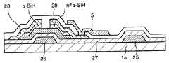
図2は、本発明で採用されるアレイ基板に適用される薄膜トランジスタ部の構造を例示する拡大断面説明図である。図2に示す如くガラス基板1a上には、Cu金属膜によって走査線25が形成され、該走査線25の一部は、薄膜トランジスタのオン・オフを制御するゲート電極26として機能する。またゲート絶縁膜27を介して走査線25と交差するように、Cu金属膜によって信号線が形成され、該信号線の一部は、薄膜トランジスタのソース電極28として機能する。このタイプは一般にボトムゲート型とも呼ばれる。 FIG. 2 is an enlarged cross-sectional explanatory view illustrating the structure of the thin film transistor portion applied to the array substrate employed in the present invention. As shown in FIG. 2, a
ゲート絶縁膜27上の画素領域には、例えばIn2O3に10質量%程度のSnOを含有させたITO膜によって形成された透明導電膜5が配置されている。Cu合金膜で形成された薄膜トランジスタのドレイン電極29は、透明導電膜5に直接コンタクトして電気的に接続される。In the pixel region on the
このTFTアレイ基板1に、走査線25を介してゲート電極26からゲート電圧を供給すると、薄膜トランジスタがオン状態となり、予め信号線に供給された駆動電圧がソース電極28からドレイン電極29を介して透明導電膜5へ供給される。そして、透明導電膜5に所定レベルの駆動電圧が供給されると、対向電極2との間に電位差が生じ、液晶層3に含まれる液晶分子が配向して光変調が行われる(図1参照)。 When a gate voltage is supplied to the
次に、TFTアレイ基板の製造工程の概略を、図3〜9の例に沿って説明する。ここでスイッチング素子として形成される薄膜トランジスタは、水素化アモルファスシリコンを半導体層として用いたアモルファスシリコンTFTを例示している。 Next, an outline of the manufacturing process of the TFT array substrate will be described with reference to FIGS. Here, the thin film transistor formed as the switching element is an amorphous silicon TFT using hydrogenated amorphous silicon as a semiconductor layer.
まずガラス基板1aに、スパッタリングで膜厚200nm程度のCu薄膜を成膜し、このCu薄膜をウェットエッチングによりパターニングしてゲート電極26と走査線25を形成する(図3)。次に、図4に示す如く、プラズマCVD法等によって膜厚300nm程度のゲート絶縁膜(シリコン窒化膜:SiNx)27を基板温度350℃程度で形成する。その上に、膜厚150nm程度の水素化アモルファスシリコン膜(a−SiH)と、膜厚50nm程度のPをドーピングしたn+型水素化アモルファスシリコン膜(n+a−SiH)を、連続して基板温度300℃程度で成膜する(図5)。First, a Cu thin film having a thickness of about 200 nm is formed on the
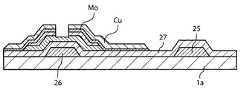
続いて図6に示す如く、水素化アモルファスシリコン膜(a−SiH)とn+型水素化アモルファスシリコン膜(n+a−SiH)をドライエッチングでパターニングする。そして図7に示す如く、膜厚50nm程度のMo(下地)と膜厚200nm程度のCu金属膜を積層成膜し、Cu/Mo積層膜をウェットエッチングでパターニングすることにより、信号線と一体のソース電極と、ITO透明導電膜にコンタクトするドレイン電極を形成する。更に、ソース電極とドレイン電極をマスクとしてn+型水素化アモルファスシリコン膜(n+a−SiH)をドライエッチングにより除去する。Subsequently, as shown in FIG. 6, the hydrogenated amorphous silicon film (a-SiH) and the n+ type hydrogenated amorphous silicon film (n+ a-SiH) are patterned by dry etching. Then, as shown in FIG. 7, Mo (underlying) with a film thickness of about 50 nm and a Cu metal film with a film thickness of about 200 nm are stacked, and the Cu / Mo stacked film is patterned by wet etching, so that it is integrated with the signal line. A source electrode and a drain electrode in contact with the ITO transparent conductive film are formed. Further, the n+ type hydrogenated amorphous silicon film (n+ a-SiH) is removed by dry etching using the source electrode and the drain electrode as a mask.
次いで図8に示す如く、プラズマCVD装置で窒化シリコン膜(SiNx)を膜厚300nm程度となる様に成膜して保護膜を形成する。この時の成膜温度は例えば250℃程度で行われることが多い。そしてこの窒化シリコン膜(SiNx)をパターニングし、ドライエッチングによって窒化シリコン膜(SiNx)にコンタクトホールを形成する。更に、酸素プラズマアッシングによるポリマー除去工程を経て、例えば非アミン系剥離液を用いたフォトレジストの剥離処理を行なった後、酸素プラズマアッシングによって生成したCu酸化膜を希フッ酸で除去する。 Next, as shown in FIG. 8, a silicon nitride film (SiNx) is formed to a thickness of about 300 nm by a plasma CVD apparatus to form a protective film. The film forming temperature at this time is often about 250 ° C., for example. Then, this silicon nitride film (SiNx) is patterned, and contact holes are formed in the silicon nitride film (SiNx) by dry etching. Furthermore, after performing a polymer removal process by oxygen plasma ashing, for example, after performing a photoresist peeling process using a non-amine-based peeling solution, the Cu oxide film generated by the oxygen plasma ashing is removed with dilute hydrofluoric acid.
最後に図9に示す如く、例えば膜厚150nm程度のITO透明導電膜を室温でスパッタ成膜し、ウェットエッチングによるパターニングを行なって画素電極(ITO透明導電膜)5を形成すると、TFTアレイ基板が完成する。 Finally, as shown in FIG. 9, for example, an ITO transparent conductive film having a film thickness of about 150 nm is formed by sputtering at room temperature and patterned by wet etching to form the pixel electrode (ITO transparent conductive film) 5. Complete.
この製造工程に沿って形成されたTFTアレイ基板は、ITO透明導電膜(画素電極)5とCu金属膜によって形成されたドレイン電極とが直接コンタクトされている。またゲート電極に繋がっている走査線のTAB部分にもITO透明導電膜5が直接コンタクトされている。 In the TFT array substrate formed along this manufacturing process, the ITO transparent conductive film (pixel electrode) 5 and the drain electrode formed by the Cu metal film are in direct contact. In addition, the ITO transparent
本発明の表示デバイスは上記の様な工程で作製されるが、本発明最大の特徴は、配線部に使用するCu合金膜として、Cuに特定の選択された元素を決められた量で含有させるところにあり、以下、この特徴点について説明する。 The display device of the present invention is manufactured by the process as described above. The greatest feature of the present invention is that Cu includes a specific selected element in a predetermined amount as a Cu alloy film used for the wiring portion. However, this feature point will be described below.
Cu合金膜に含有させる元素としては、Znおよび/またはMg、もしくはNiおよび/またはMnが選択される。これらの元素は、Cu金属には固溶するがCu酸化膜には固溶しない元素として選択したものであり、これらの元素が固溶しているCu合金が酸化されると、これらの元素(Zn,Ni,Mn,Mg)はCu酸化膜に固溶しないため、これらの元素は酸化により生成したCu酸化膜の界面下に掃き出されて濃化され、該濃化層によってCu酸化膜の更なる成長を抑制する。このため、酸素アッシングやITO透明導電膜との積層成膜工程でも、Cu酸化膜の成長が最小限に抑えられ、特にITO積層成膜では、Cu合金膜と透明導電膜とが良好な電気的コンタクト状態に保たれる。 As an element to be contained in the Cu alloy film, Zn and / or Mg, or Ni and / or Mn are selected. These elements are selected as elements that are dissolved in Cu metal but not in the Cu oxide film. When a Cu alloy in which these elements are dissolved is oxidized, these elements ( Since Zn, Ni, Mn, and Mg) do not dissolve in the Cu oxide film, these elements are swept out and concentrated under the interface of the Cu oxide film generated by the oxidation, and the concentrated layer forms the Cu oxide film. Suppress further growth. For this reason, the growth of the Cu oxide film can be suppressed to the minimum even in the process of stacking the film with oxygen ashing or the ITO transparent conductive film. Stay in contact.
こうした濃化層の形成によって、例えば10−5Ω・cm2台〜10−4Ω・cm2台の低いコンタクト抵抗率を得るには、上記Zn,Ni,Mn,Mgから選ばれる1種以上の元素を、総量で0.1原子%以上、より好ましくは0.2原子%以上含有させるのがよく、これにより、バリアメタルを介在させることなく直接接続で十分な導電性を確保することができ、液晶ディスプレイの階調表示などの表示性能の劣化を防止できる。その結果、バリアメタル成膜工程の省略によるタクトタイムの短縮によって大幅な生産性アップが可能となる。In order to obtain a low contact resistivity of, for example, 10−5 Ω · cm2 to 10−4 Ω · cm2 by forming such a concentrated layer, one or more selected from the above Zn, Ni, Mn, and Mg These elements should be contained in a total amount of 0.1 atomic% or more, more preferably 0.2 atomic% or more, so that sufficient conductivity can be secured by direct connection without interposing a barrier metal. It is possible to prevent deterioration of display performance such as gradation display of the liquid crystal display. As a result, the productivity can be significantly increased by shortening the tact time by omitting the barrier metal film forming step.
Cu合金膜中へ混入させる上記元素の量は、熱処理による電気抵抗率の低下も考慮して、Znおよび/またはMgの場合は総量で3.0原子%以下、より好ましくは2.0原子%以下、Niおよび/またはMnの場合は総量で0.5原子%以下、より好ましくは0.4原子%以下に抑えるのがよい。 The amount of the element mixed into the Cu alloy film is, in consideration of a decrease in electrical resistivity due to heat treatment, in the case of Zn and / or Mg, a total amount of 3.0 atomic% or less, more preferably 2.0 atomic%. Hereinafter, in the case of Ni and / or Mn, the total amount is preferably 0.5 atomic% or less, more preferably 0.4 atomic% or less.
Cu金属膜は、後工程の熱処理に起因する引張応力により、ボイドと呼ばれる粒界割れの様な欠陥を発生することがあるが、上記の様にZn,Ni,Mn,Mgの1種以上と共にFeとP、またはCoとPを含有させると、これらが熱処理時にFePやCoP化合物として粒界に微小析出し、粒界を強化する作用を発揮してボイドの発生を抑える。従って、成膜後に300℃を超える高温の熱履歴を受ける場合は、上記Zn,Ni,Mn,Mgの1種以上と共に、Feおよび/またはCoを総量で0.02〜1.0原子%と、Pを0.005〜0.5原子%添加することが好ましい。 The Cu metal film may generate defects such as intergranular cracks called voids due to the tensile stress resulting from the heat treatment in the post-process, but with one or more of Zn, Ni, Mn, and Mg as described above. When Fe and P or Co and P are contained, they are finely precipitated at the grain boundaries as FeP or CoP compounds during the heat treatment, and exert an effect of strengthening the grain boundaries to suppress the generation of voids. Therefore, when receiving a high-temperature thermal history exceeding 300 ° C. after film formation, the total amount of Fe and / or Co is 0.02 to 1.0 atomic% together with one or more of Zn, Ni, Mn, and Mg. , P is preferably added in an amount of 0.005 to 0.5 atomic%.
前記透明導電膜としては、前述した通り酸化インジウム錫(ITO)が多用されるが、酸化インジウム亜鉛(IZO)を用いても勿論構わない。 As the transparent conductive film, indium tin oxide (ITO) is frequently used as described above, but indium zinc oxide (IZO) may of course be used.
前記Cu合金に透明導電膜を積層し、タブ接続電極として使用した表示デバイスも好ましい態様である。 A display device in which a transparent conductive film is laminated on the Cu alloy and used as a tab connection electrode is also a preferred embodiment.
以下、実施例を挙げて本発明の構成および作用効果をより具体的に説明するが、本発明はもとより下記実施例によって制限を受けるものではない。 EXAMPLES Hereinafter, although an Example is given and the structure and effect of this invention are demonstrated more concretely, this invention is not restrict | limited by the following Example from the first.
実施例
純Cuスパッタリングターゲット(サイズ:直径101.6mm×厚さ5mm)に、後記表1〜13に示す合金元素のチップ(サイズ:5mm×5mm×厚さ1mm)を所定数配置した複合スパッタリングターゲットと、スパッタリング装置(島津製作所製:「HSM−552」)を使用し、DCマグネトロンスパッタリング法(背圧:0.27×10−3Pa以下、Arガス圧:0.27Pa、Arガス流量:30sccm、スパッタパワー:DC200W、極間距離:50.4mm、基板温度:室温)によって、ガラス基板(コーニング社製の#1737、サイズは、電気抵抗率と耐熱性の評価用が直径50.8mm×厚さ0.7mm、コンタクト抵抗率評価用が直径101.6mm×厚さ0.7mm)上に、純Cu(試料番号1)、Cu−Zn合金(試料番号2〜6)、Cu−Mg合金(試料番号7〜11)、Cu−Mn合金(試料番号12〜16)、Cu−Ni合金(試料番号17〜21)、Cu−Zn−Fe−P合金(試料番号22〜26)、Cu−Mg−Fe−P合金(試料番号27〜31)、Cu−Mn−Fe−P合金(試料番号32〜36)、Cu−Ni−Fe−P合金(試料番号37〜41)、Cu−Zn−Mg合金(試料番号42〜45)、Cu−Mn−Ni合金(試料番号46〜49)、Cu−Zn−Co−P合金(試料番号50〜54)、Cu−Mg−Co−P合金(試料番号55〜59)、Cu−Mn−Co−P合金(試料番号60〜64)、Cu−Ni−Co−P合金(試料番号65〜69)、の薄膜を膜厚300nmで形成した。Example Composite sputtering target in which a predetermined number of alloy element chips (size: 5 mm × 5 mm × thickness 1 mm) shown in Tables 1 to 13 below are arranged on a pure Cu sputtering target (size: diameter 101.6 mm × thickness 5 mm) And a sputtering apparatus (manufactured by Shimadzu Corporation: “HSM-552”), DC magnetron sputtering method (back pressure: 0.27 × 10⁻³ Pa or less, Ar gas pressure: 0.27 Pa, Ar gas flow rate: 30 sccm , Sputtering power: DC 200 W, distance between electrodes: 50.4 mm, substrate temperature: room temperature), glass substrate (# 1737 manufactured by Corning), size is 50.8 mm diameter x thickness for evaluation of electrical resistivity and heat resistance 0.7 mm in diameter, 101.6 mm in diameter for contact resistivity evaluation x 0.7 mm in thickness) and pure Cu (sample number 1) Cu—Zn alloy (sample numbers 2 to 6), Cu—Mg alloy (sample numbers 7 to 11), Cu—Mn alloy (sample numbers 12 to 16), Cu—Ni alloy (sample numbers 17 to 21), Cu— Zn-Fe-P alloy (sample numbers 22-26), Cu-Mg-Fe-P alloy (sample numbers 27-31), Cu-Mn-Fe-P alloy (sample numbers 32-36), Cu-Ni- Fe-P alloy (sample numbers 37 to 41), Cu-Zn-Mg alloy (sample numbers 42 to 45), Cu-Mn-Ni alloy (sample numbers 46 to 49), Cu-Zn-Co-P alloy (sample) No. 50 to 54), Cu—Mg—Co—P alloy (sample numbers 55 to 59), Cu—Mn—Co—P alloy (sample numbers 60 to 64), Cu—Ni—Co—P alloy (sample number 65) ˜69) was formed with a film thickness of 300 nm.
そして、これら評価用薄膜の金属組成をICP(Inductively Coupled Plasma)発光分析法またはICP質量分析法によって調べると共に、下記の方法で電気抵抗率、コンタクト抵抗率および耐熱性を評価した。 And while examining the metal composition of these thin films for evaluation by ICP (Inductively Coupled Plasma) emission analysis or ICP mass spectrometry, the electrical resistivity, contact resistivity, and heat resistance were evaluated by the following methods.
[電気抵抗率]
ガラス基板(コーニング社製の#1737、サイズは直径50.8mm×厚さ0.7mm)上に形成された各Cu薄膜を、フォトリソグラフィーとウエットエッチングによって線幅100μm、線長10mmの電気抵抗評価用パターンに加工した。この際、ウエットエッチャントとしては、硫酸:硝酸:酢酸=50:10:10の混酸からなる混合液を用いた。そして、真空熱処理装置により250℃×30分または350℃×30分の真空熱処理(真空度:0.27×10⁻³Pa以下)を施し、この真空熱処理の前後で、夫々の電気抵抗を直流四探針法により室温で測定した。[Electric resistivity]
Electrical resistance evaluation of each Cu thin film formed on a glass substrate (# 1737 manufactured by Corning Inc., diameter: 50.8 mm × thickness: 0.7 mm) with a line width of 100 μm and a line length of 10 mm by photolithography and wet etching Processed into a pattern. At this time, as the wet etchant, a mixed solution composed of a mixed acid of sulfuric acid: nitric acid: acetic acid = 50: 10: 10 was used. Then, vacuum heat treatment (250 ° C. × 30 minutes or 350 ° C. × 30 minutes) is performed by a vacuum heat treatment apparatus (vacuum degree: 0.27 × 10⁻³ Pa or less), and before and after this vacuum heat treatment, the electric resistance is changed to direct current. Measurement was performed at room temperature by the four-probe method.
上記工程によって各Cu薄膜の電気抵抗率を測定する。電気抵抗率の合否判定は、250℃×30min熱処理後の電気抵抗率が5.0μΩ・cm未満であるものを合格(○)、5.0μΩ・cm以上であるものを不合格(×)とし、350℃×30min熱処理後の電気抵抗率が4.0μΩ・cm未満であるものを合格(○)、4.0μΩ・cm以上であるものを不合格(×)とした。 The electrical resistivity of each Cu thin film is measured by the above process. For the pass / fail judgment of electrical resistivity, the electrical resistivity after heat treatment at 250 ° C. for 30 minutes is less than 5.0 μΩ · cm, and the pass (◯) is 5.0 μΩ · cm or more is rejected (×). A sample having an electrical resistivity of less than 4.0 μΩ · cm after heat treatment at 350 ° C. for 30 minutes was determined to be acceptable (◯) and a sample having an electrical resistivity of 4.0 μΩ · cm or higher was rejected (×).
表1,2に、250℃×30minもしくは350℃×30min熱処理した後に測定した電気抵抗率を示す。この表から明らかな様に、ZnとMgの合計が3.0原子%未満もしくは、NiとMnの合計が0.5原子%未満の場合、電気抵抗率の目標値(250℃×30min熱処理後:5.0μΩcm、350℃×30min熱処理後:4.0μΩcm)を満たしている。また、更にFeまたはCoの合計含量が1.0原子%以下で、かつP含量が0.5原子%以下である場合も、電気抵抗率の目標値(250℃×30min:5.0μΩcm、350℃×30min熱処理後:4.0μΩcm)を満たしている。 Tables 1 and 2 show the electrical resistivity measured after heat treatment at 250 ° C. × 30 min or 350 ° C. × 30 min. As is apparent from this table, when the total of Zn and Mg is less than 3.0 atomic% or the total of Ni and Mn is less than 0.5 atomic%, the target value of electrical resistivity (after heat treatment at 250 ° C. × 30 min : 5.0 μΩcm, 350 ° C. × 30 min after heat treatment: 4.0 μΩcm). Further, when the total content of Fe or Co is 1.0 atomic% or less and the P content is 0.5 atomic% or less, the target value of electric resistivity (250 ° C. × 30 min: 5.0 μΩcm, 350 ° C x 30 min after heat treatment: 4.0 μΩcm).

[コンタクト抵抗率・ドライエッチングプロセス]
コンタクト抵抗率のエッチングプロセス依存性を調べるため、ドライエッチングプロセスにより形成したコンタクトホールについてコンタクト抵抗率を測定した。コンタクトを形成するプロセスの詳細は下記の通りである。[Contact resistivity / Dry etching process]
In order to investigate the etching process dependency of the contact resistivity, the contact resistivity was measured for the contact hole formed by the dry etching process. Details of the process for forming the contact are as follows.
ガラス基板上に成膜した各Cu薄膜に対し、プラズマCVD装置によってSiN薄膜を膜厚300nmで成膜する。基板加熱温度は250℃または350℃とし、ガラス基板の予備加熱とCVD処理も含めた正味の熱処理時間は0.5時間とする。 For each Cu thin film formed on the glass substrate, a SiN thin film is formed with a film thickness of 300 nm by a plasma CVD apparatus. The substrate heating temperature is 250 ° C. or 350 ° C., and the net heat treatment time including preheating and CVD treatment of the glass substrate is 0.5 hour.
次にコンタクトホールのフォトリソグラフィーを行い、ICP型ドライエッチャーを用いてドライエッチングによりSiNにコンタクトホール(10×10μm角:1個)を形成する。その後、酸素アッシングおよび非アミン系レジスト剥離液に浸漬してレジストを剥離し、バッファードフッ酸(BHF)でコンタクト底面を洗浄する。次にRFマグネトロンスパッタリング法によってITO膜を成膜し、フォトリソグラフィーとウエットエッチングによりITO薄膜を線幅100μm、線長400mmのケルビンパターンに加工する。この時、ウエットエッチャントとしては、ナガセケムテックス社製のITOエッチング液を使用する。抵抗率の測定は四端子法によって行い、Cu/ITO界面のコンタクト部分での電圧降下分からコンタクト抵抗値を測定し、既知のコンタクトホール面積とコンタクト抵抗値から単位面積当たりのコンタクト抵抗率を算出した。 Next, contact hole photolithography is performed, and a contact hole (10 × 10 μm square: 1 piece) is formed in SiN by dry etching using an ICP type dry etcher. Thereafter, the resist is removed by dipping in an oxygen ashing and non-amine resist stripping solution, and the contact bottom surface is washed with buffered hydrofluoric acid (BHF). Next, an ITO film is formed by RF magnetron sputtering, and the ITO thin film is processed into a Kelvin pattern having a line width of 100 μm and a line length of 400 mm by photolithography and wet etching. At this time, ITO etchant manufactured by Nagase ChemteX Corporation is used as the wet etchant. The resistivity was measured by the four probe method, the contact resistance value was measured from the voltage drop at the contact portion at the Cu / ITO interface, and the contact resistivity per unit area was calculated from the known contact hole area and contact resistance value. .
上記工程により、各Cu薄膜とITO薄膜とのコンタクト抵抗の測定が可能なケルビンパターンを製作してコンタクト抵抗を測定する。コンタクト抵抗の合否判定は、測定箇所100点のうち最大値5点、最小値5点を除く合計90点の平均のコンタクト抵抗率が5×10⁻⁴Ω・cm2未満のものを合格(○)、この値以上のものを不合格(×)とした。またバラツキの評価に関しては、100箇所の測定結果のうち5×10⁻⁴Ω・cm2を超えるコンタクト抵抗率を示す割合(不良率)が10%未満である場合を合格(○)、10%以上である場合を不合格(×)とする。Through the above process, a Kelvin pattern capable of measuring the contact resistance between each Cu thin film and the ITO thin film is manufactured, and the contact resistance is measured. For the determination of pass / fail of the contact resistance, an average contact resistivity of a total of 90 points excluding the maximum value of 5 points and the minimum value of 5 points out of 100 measurement points is less than 5 × 10⁻⁴ Ω · cm2 (○ ), Those above this value were determined to be rejected (x). In addition, regarding the evaluation of variation, a case where the ratio (failure rate) indicating a contact resistivity exceeding 5 × 10⁻⁴ Ω · cm2 out of 100 measurement results is less than 10% is acceptable (◯), 10% The case where it is above is set as a disqualification (x).
250℃または350℃でCVD成膜および熱処理を行い、ドライプロセスでコンタクトホールを形成した試料のコンタクト抵抗率の評価結果を、下記表3〜5および表6〜8に示す。表3〜8からも分かる様に、純Cu,Cu合金のいずれについても、平均コンタクト抵抗率の合格基準を満たしている。但し、純Cuに比べて、Zn,Ni,Mn,Mgから選ばれる1以上の元素の総含有量が0.1原子%以上であるCu−(Zn,Ni,Mn,Mg)合金、およびCu−(Zn,Ni,Mn,Mg)−(Fe,Co)−P合金膜は、コンタクト抵抗率のバラツキが小さく、信頼性の高い低コンタクト抵抗率が得られている。 Tables 3 to 5 and Tables 6 to 8 below show the evaluation results of contact resistivity of samples in which CVD film formation and heat treatment are performed at 250 ° C. or 350 ° C. and contact holes are formed by a dry process. As can be seen from Tables 3 to 8, both the pure Cu and Cu alloys satisfy the acceptance criteria for average contact resistivity. However, compared to pure Cu, a Cu— (Zn, Ni, Mn, Mg) alloy having a total content of one or more elements selected from Zn, Ni, Mn, and Mg of 0.1 atomic% or more, and Cu The-(Zn, Ni, Mn, Mg)-(Fe, Co) -P alloy film has small variations in contact resistivity and a low contact resistivity with high reliability.
[コンタクト抵抗率・ウエットエッチングプロセス]
コンタクト抵抗率のエッチングプロセス依存性を調べるため、ウエットエッチングプロセスにより形成したコンタクトホールについてコンタクト抵抗率を測定した。コンタクトを形成するプロセスの詳細は下記の通りである。[Contact resistivity / wet etching process]
In order to investigate the dependency of the contact resistivity on the etching process, the contact resistivity was measured for the contact hole formed by the wet etching process. Details of the process for forming the contact are as follows.
ガラス基板上に成膜した各Cu薄膜に対して、プラズマCVD装置によってSiN薄膜を膜厚300nmで成膜する。基板加熱温度は250℃または350℃とし、ガラス基板の予備加熱とCVD処理も含めた正味の熱処理時間は0.5時間とする。 For each Cu thin film formed on a glass substrate, a SiN thin film is formed with a film thickness of 300 nm by a plasma CVD apparatus. The substrate heating temperature is 250 ° C. or 350 ° C., and the net heat treatment time including preheating and CVD treatment of the glass substrate is 0.5 hour.
次にコンタクトホールのフォトリソグラフィーを行い、ウエットエッチングによりSiNにコンタクトホール(10×10μm角:1個)を形成する。ウエットエッチングにはバッファードフッ酸を使用する。その後、RFマグネトロンスパッタリング法によってITO膜を成膜し、フォトリソグラフィーとウエットエッチングによりITO薄膜を線幅100μm、線長400mmのケルビンパターンに加工し、コンタクト抵抗値を評価する。この時、ウエットエッチャントとしては、ナガセケムテックス社製のITOエッチング液を使用する。抵抗率の測定は、四端子法によって同形状のパターンで100点行い、Cu/ITO界面のコンタクト部分での電圧降下分からコンタクト抵抗値を測定し、既知のコンタクトホール面積とコンタクト抵抗値から単位面積当たりのコンタクト抵抗率を算出する。 Next, contact hole photolithography is performed, and contact holes (10 × 10 μm square: one) are formed in SiN by wet etching. Buffered hydrofluoric acid is used for wet etching. Thereafter, an ITO film is formed by RF magnetron sputtering, and the ITO thin film is processed into a Kelvin pattern having a line width of 100 μm and a line length of 400 mm by photolithography and wet etching, and the contact resistance value is evaluated. At this time, ITO etchant manufactured by Nagase ChemteX Corporation is used as the wet etchant. The resistivity is measured at 100 points in the same shape pattern by the four-terminal method, the contact resistance value is measured from the voltage drop at the contact portion of the Cu / ITO interface, and the unit area is determined from the known contact hole area and contact resistance value. The contact resistivity per unit is calculated.
上記工程により各Cu薄膜とITO薄膜とのコンタクト抵抗の測定が可能なケルビンパターンを製作し、コンタクト抵抗を測定する。コンタクト抵抗の合否判定は、測定箇所100点のうち最大値5点、最小値5点を除く合計90点の平均のコンタクト抵抗率が5×10⁻⁴Ω・cm2未満のものを合格(○)、この値以上のものを不合格(×)とした。またバラツキの評価に関しては、100箇所の測定結果のうち5×10⁻⁴Ω・cm2を超えるコンタクト抵抗率を示す割合(不良率)が10%未満である場合を合格(○)、10%以上である場合を不合格(×)とする。A Kelvin pattern capable of measuring the contact resistance between each Cu thin film and the ITO thin film is manufactured by the above process, and the contact resistance is measured. For the determination of pass / fail of the contact resistance, an average contact resistivity of a total of 90 points excluding the maximum value of 5 points and the minimum value of 5 points out of 100 measurement points is less than 5 × 10⁻⁴ Ω · cm2 (○ ), Those above this value were determined to be rejected (x). In addition, regarding the evaluation of variation, a case where the ratio (failure rate) indicating a contact resistivity exceeding 5 × 10⁻⁴ Ω · cm2 out of 100 measurement results is less than 10% is acceptable (◯), 10% The case where it is above is set as a disqualification (x).
250℃または350℃でCVD成膜および熱処理を行い、ウエットエッチングプロセスでコンタクトホールを形成した試料のコンタクト抵抗率の評価結果を、下記表3〜8に示す。これらの表からも分かる様に、バラツキに関しては、純Cuに比べて、Zn,Ni,Mn,Mgから選ばれる1以上の元素の総含有量が0.1原子%以上であるCu−(Zn,Ni,Mn,Mg)合金、およびCu−(Zn,Ni,Mn,Mg)−(Fe,Co)−P合金膜の方が優れている。但し、純Cu、Cu合金のいずれも、平均コンタクト抵抗率とバラツキの判定基準を満足しており、良好なコンタクトを実現していることが分かる。 Tables 3 to 8 below show the evaluation results of the contact resistivity of the samples in which the CVD film formation and the heat treatment were performed at 250 ° C. or 350 ° C. and the contact holes were formed by the wet etching process. As can be seen from these tables, regarding the variation, Cu— (Zn) in which the total content of one or more elements selected from Zn, Ni, Mn, and Mg is 0.1 atomic% or more compared to pure Cu. , Ni, Mn, Mg) and Cu— (Zn, Ni, Mn, Mg) — (Fe, Co) —P alloy films are superior. However, it can be seen that both pure Cu and Cu alloy satisfy the determination criteria of average contact resistivity and variation, and realize good contact.
[コンタクト抵抗率・コンタクト信頼性試験]
ウエットエッチングにより上記と同様の方法でコンタクト形成を行った後、意図的に酸素アッシングを行うことによってコンタクト信頼性試験を行った。これは、Cu・Cu合金膜を大気中に保管したときの大気酸化を模擬したもので、コンタクトを形成するプロセスの詳細は下記の通りである。[Contact Resistance / Contact Reliability Test]
After contact formation by wet etching in the same manner as described above, a contact reliability test was performed by intentionally performing oxygen ashing. This is a simulation of atmospheric oxidation when the Cu / Cu alloy film is stored in the atmosphere, and details of the process for forming the contact are as follows.
ガラス基板上に成膜した各Cu薄膜に対して、フォトリソグラフィーとウエットエッチングを施して配線加工を行う。ウエットエッチャントとしては、硫酸:硝酸:酢酸=50:10:10の混酸を使用する。次に、プラズマCVD装置によってSiN薄膜を膜厚300nmで成膜する。基板加熱温度は250℃または350℃とし、ガラス基板の予備加熱とCVD処理も含めた正味の熱処理時間は0.5時間とする。 Each Cu thin film formed on the glass substrate is subjected to wiring processing by performing photolithography and wet etching. As the wet etchant, a mixed acid of sulfuric acid: nitric acid: acetic acid = 50: 10: 10 is used. Next, a SiN thin film is formed with a film thickness of 300 nm by a plasma CVD apparatus. The substrate heating temperature is 250 ° C. or 350 ° C., and the net heat treatment time including preheating and CVD treatment of the glass substrate is 0.5 hour.
次にコンタクトホールのフォトリソグラフィーを行い、SiNのコンタクトエッチをウエットエッチングによって行う。ウエットエッチングにはバッファードフッ酸を使用する。その後、アッシング装置を用いて酸素雰囲気でアッシング処理を行って、コンタクト底面を酸化させる。次いで、これらの試料に対してRFマグネトロンスパッタ装置で膜厚100nmのITO膜を成膜し、その後、フォトリソグラフィーおよびウエットエッチングを行い、コンタクト抵抗値のアッシング時間依存性を評価する。抵抗率の測定は四端子法によって同形状のパターンで100点行い、Cu/ITO界面のコンタクト部分での電圧降下分からコンタクト抵抗値を測定し、既知のコンタクトホール面積とコンタクト抵抗値から単位面積当たりのコンタクト抵抗率を算出する。 Next, contact hole photolithography is performed, and SiN contact etching is performed by wet etching. Buffered hydrofluoric acid is used for wet etching. Thereafter, an ashing process is performed in an oxygen atmosphere using an ashing apparatus to oxidize the contact bottom surface. Next, an ITO film having a film thickness of 100 nm is formed on these samples with an RF magnetron sputtering apparatus, and thereafter, photolithography and wet etching are performed to evaluate the ashing time dependency of the contact resistance value. The resistivity is measured at 100 points in the same shape pattern by the four-terminal method, the contact resistance value is measured from the voltage drop at the contact portion of the Cu / ITO interface, and the unit area is calculated from the known contact hole area and contact resistance value. The contact resistivity is calculated.
上記工程により各Cu薄膜とITO薄膜とのコンタクト抵抗の測定が可能なケルビンパターンを製作し、コンタクト抵抗を測定する。コンタクト抵抗の合否判定は、測定箇所100点のうち最大値5点、最小値5点を除く合計90点の平均のコンタクト抵抗率が5×10⁻⁴Ω・cm2未満のものを合格(○)、この値以上のものを不合格(×)とした。またバラツキの評価に関しては、100箇所の測定結果のうち5×10⁻⁴Ω・cm2を超えるコンタクト抵抗率を示す割合(不良率)が10%未満である場合を合格(○)、10%以上である場合を不合格(×)とする。A Kelvin pattern capable of measuring the contact resistance between each Cu thin film and the ITO thin film is manufactured by the above process, and the contact resistance is measured. For the determination of pass / fail of the contact resistance, an average contact resistivity of a total of 90 points excluding the maximum value of 5 points and the minimum value of 5 points out of 100 measurement points is less than 5 × 10⁻⁴ Ω · cm2 (○ ), Those above this value were determined to be rejected (x). In addition, regarding the evaluation of variation, a case where the ratio (failure rate) indicating a contact resistivity exceeding 5 × 10⁻⁴ Ω · cm2 out of 100 measurement results is less than 10% is acceptable (◯), 10% The case where it is above is set as a disqualification (x).
250℃または350℃でCVD成膜および熱処理を行い、ウエットプロセスでコンタクトホールを形成した後にアッシング処理を10min行った試料のコンタクト抵抗率の評価結果を、下記表3〜8に示す。表3〜8からも分かる様に、純Cuはコンタクト抵抗率が高く、またバラツキも大きい。一方、純Cuに比べて、Zn,Ni,Mn,Mgから選ばれる1以上の元素の総含有量が0.1原子%以上であるCu−(Zn,Ni,Mn,Mg)合金、およびCu−(Zn,Ni,Mn,Mg)−(Fe,Co)−P合金膜は、平均コンタクト抵抗率が低く且つバラツキも小さく、良好なコンタクトを実現していることが分かる。このことは、上記Cu合金を使用することで大気酸化を受け難くなり、製造工程中のプロセスマージンが改善されることを示している。 Tables 3 to 8 below show the evaluation results of contact resistivity of samples obtained by performing CVD film formation and heat treatment at 250 ° C. or 350 ° C., forming contact holes by a wet process, and performing ashing treatment for 10 minutes. As can be seen from Tables 3 to 8, pure Cu has a high contact resistivity and a large variation. On the other hand, compared to pure Cu, a Cu— (Zn, Ni, Mn, Mg) alloy having a total content of one or more elements selected from Zn, Ni, Mn, and Mg of 0.1 atomic% or more, and Cu It can be seen that the — (Zn, Ni, Mn, Mg) — (Fe, Co) —P alloy film has a low average contact resistivity and a small variation, and realizes a good contact. This indicates that the use of the Cu alloy makes it difficult to undergo atmospheric oxidation, and the process margin during the manufacturing process is improved.
[耐熱性]
フォトレジストとしてクラリアントジャパン社製の「AZ P4110」、フォトレジスト現像液として同社製の「AZデベロッパー」を用いたフォトリソグラフィー(工程:フォトレジスト塗布→プリベーキング→露光→フォトレジスト現像→水洗→乾燥)と、硫酸:硝酸:酢酸=50:10:10の混酸からなるウエットエッチャントを用いたウエットエッチング(工程:ウエットエッチング→水洗→乾燥→フォトレジスト剥離→乾燥)を行い、評価用の各Cu薄膜を線幅/線間隔=10μm/10μmのストライプパターン形状に加工した。その後、各Cu薄膜に対し350℃で30分の真空熱処理(真空度:0.27×10−3Pa以下)を施し、熱処理後に試料表面をウエットエッチャントで約10nmのライトエッチィングを行い、各Cu薄膜の耐熱性を評価した。[Heat-resistant]
Photolithography using “AZ P4110” manufactured by Clariant Japan as a photoresist and “AZ Developer” manufactured by the company as a photoresist developer (process: photoresist application → pre-baking → exposure → photoresist development → water washing → drying) And wet etching using a wet etchant composed of a mixed acid of sulfuric acid: nitric acid: acetic acid = 50: 10: 10 (process: wet etching → washing → drying → photoresist peeling → drying) Line width / line interval = 10 μm / 10 μm was processed into a stripe pattern shape. Thereafter, each Cu thin film was subjected to a vacuum heat treatment at 350 ° C. for 30 minutes (vacuum degree: 0.27 × 10⁻³ Pa or less), and after the heat treatment, the sample surface was light-etched with a wet etchant to a thickness of about 10 nm. The heat resistance of the Cu thin film was evaluated.
Cu膜は、熱処理を行うと配線の上面および側面に凹状の欠陥(ボイド)が発生する。そこで、熱処理後のCu表面をライトエッチィングすることで、熱処理により発生したボイドをエンハンスして光学顕微鏡で観察し、単位面積当たりのボイド密度を測定した。そして、ボイド密度が1.0×10⁸個/m2以下のものを優秀(◎)、1.0×108個/m2を超え1.0×1010個/m2以下のものを良好(○)(◎,○はいずれも合格)、1.0×1010個/m2超のものを不合格(×)とした。When heat treatment is performed on the Cu film, concave defects (voids) are generated on the upper and side surfaces of the wiring. Therefore, light-etching was performed on the Cu surface after the heat treatment to enhance voids generated by the heat treatment, and observed with an optical microscope, and the void density per unit area was measured. And those having a void density of 1.0 × 10⁸ pieces / m2 or less are excellent (◎), and those having a void density exceeding 1.0 × 10⁸ pieces / m2 and 1.0 × 10¹⁰ pieces / m2 or less. Good (◯) (◎ and ○ are both acceptable) and those exceeding 1.0 × 10¹⁰ / m2 were determined to be rejected (×).
結果は表9,10に示す通りであり、350℃×30minの真空熱処理を行った場合、純Cuでは耐熱性が不十分であるのに対し、Zn,Ni,Mn,Mgから選ばれる1以上の元素の総含有量が0.1原子%以上であるCu−(Zn,Ni,Mn,Mg)合金膜は、十分な耐熱性を有している。また、FeまたはCoとPを含有するCu−(Zn,Ni,Mn,Mg)−(Fe,Co)−P合金膜は、更に優れた耐熱性を有していることが分かる。 The results are as shown in Tables 9 and 10, and when heat treatment is performed at 350 ° C. for 30 minutes, pure Cu has insufficient heat resistance, whereas one or more selected from Zn, Ni, Mn, and Mg. A Cu— (Zn, Ni, Mn, Mg) alloy film having a total content of the above elements of 0.1 atomic% or more has sufficient heat resistance. Further, it can be seen that the Cu— (Zn, Ni, Mn, Mg) — (Fe, Co) —P alloy film containing Fe or Co and P has more excellent heat resistance.
上記実験で得た合否判定結果を表11〜13に纏めて示す。これらの表からも明らかな様に、Cu中に含まれる所定の合金元素の含有量が不足する場合は、コンタクト抵抗率の低減効果が不足気味となり、逆に多過ぎると、Cu合金膜自体の電気抵抗率が高くなり、いずれも本発明の目的にそぐわなくなる。 The pass / fail judgment results obtained in the above experiments are summarized in Tables 11-13. As is clear from these tables, when the content of the predetermined alloy element contained in Cu is insufficient, the effect of reducing the contact resistivity is insufficient, and conversely, if too much, the Cu alloy film itself The electrical resistivity will be high and none will meet the purpose of the present invention.
そして、Cuに添加する合金元素の種類と量を適切に制御することで、本発明に係る表示デバイスにおけるCu合金膜と透明導電膜との界面に酸化膜が生じる様なプロセス環境下においても、低抵抗の直接接続が可能となる。また、更にFeやCoとPを複合添加したものの耐熱性は特に良好であり、高温の熱履歴を受ける場合に好適である。従って、このTFTアレイ基板を備えた平面表示装置としての液晶表示装置であれば、画素電極(透明電極)と直接配線部との間でコンタクト抵抗の増大およびバラツキを最小限に抑えることができるので、表示画面の品位に与える悪影響を防止することができ、表示品位を大幅に改善できる。 And by appropriately controlling the type and amount of the alloy element added to Cu, even in a process environment where an oxide film is generated at the interface between the Cu alloy film and the transparent conductive film in the display device according to the present invention, Direct connection with low resistance is possible. In addition, the heat resistance of the composite addition of Fe, Co, and P is particularly good, and is suitable when receiving a high-temperature thermal history. Therefore, in the case of a liquid crystal display device as a flat display device provided with this TFT array substrate, it is possible to minimize an increase and variation in contact resistance between the pixel electrode (transparent electrode) and the direct wiring portion. The adverse effect on the display screen quality can be prevented, and the display quality can be greatly improved.
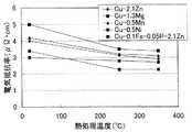
図10は、上記実験のうち代表的な試料について、熱処理温度と電気抵抗率の関係を示したグラフである。この図からも分かる様に、何れの試料についても、100〜400℃の熱履歴で電気抵抗率は明らかに低下している。なお液晶の一般的な製造工程では、Cu配線の形成後に250〜350℃程度の熱処理温度が加わる。 FIG. 10 is a graph showing the relationship between the heat treatment temperature and the electrical resistivity for a representative sample among the above experiments. As can be seen from this figure, the electrical resistivity of each sample is clearly reduced with a thermal history of 100 to 400 ° C. In a general manufacturing process of liquid crystal, a heat treatment temperature of about 250 to 350 ° C. is applied after the formation of the Cu wiring.
図11は、上記実験のうち代表的な試料について、熱処理温度とボイド密度の関係を示したグラフであり、熱処理温度が250℃では、Zn,Mg,Mn,Niから選ばれる1以上の元素を添加することで、ボイドの発生を抑制できる。更に高温である350℃の熱履歴を受ける場合は、FeやPを添加したCu合金を使用することで、ボイドの発生を大幅に抑制できることが分かる。 FIG. 11 is a graph showing the relationship between the heat treatment temperature and the void density for a representative sample among the above experiments. When the heat treatment temperature is 250 ° C., one or more elements selected from Zn, Mg, Mn, and Ni are added. By adding, generation | occurrence | production of a void can be suppressed. Furthermore, when receiving the heat history of 350 degreeC which is high temperature, it turns out that generation | occurrence | production of a void can be suppressed significantly by using Cu alloy which added Fe and P. FIG.
上記実験結果からも明らかな様に、本発明に係る表示デバイスにおけるCu合金膜と透明導電膜との界面には、従来例の様なバリアメタルなしでも低抵抗の直接接続が可能となる。従って、このTFTアレイ基板を備えた平面表示装置としての液晶表示装置であれば、画素電極(透明電極膜)と接続配線部との間でコンタクト抵抗の増大を最小限に抑えることができるので、表示画面の品位に与える悪影響を防止することができ、表示品位を大幅に改善できる。 As is clear from the above experimental results, a low resistance direct connection can be made to the interface between the Cu alloy film and the transparent conductive film in the display device according to the present invention without a barrier metal as in the conventional example. Therefore, in the case of a liquid crystal display device as a flat display device provided with this TFT array substrate, an increase in contact resistance between the pixel electrode (transparent electrode film) and the connection wiring portion can be minimized. The adverse effect on the quality of the display screen can be prevented, and the display quality can be greatly improved.
Claims (5)
Translated fromJapanesePriority Applications (5)
| Application Number | Priority Date | Filing Date | Title |
|---|---|---|---|
| JP2005272643AJP4542008B2 (en) | 2005-06-07 | 2005-09-20 | Display device |
| US11/431,580US20060275618A1 (en) | 2005-06-07 | 2006-05-11 | Display device |
| TW095117334ATWI336803B (en) | 2005-06-07 | 2006-05-16 | Display device |
| KR1020060050401AKR100802879B1 (en) | 2005-06-07 | 2006-06-05 | Display device |
| SG200603839ASG128578A1 (en) | 2005-06-07 | 2006-06-06 | Display device |
Applications Claiming Priority (2)
| Application Number | Priority Date | Filing Date | Title |
|---|---|---|---|
| JP2005167185 | 2005-06-07 | ||
| JP2005272643AJP4542008B2 (en) | 2005-06-07 | 2005-09-20 | Display device |
Publications (2)
| Publication Number | Publication Date |
|---|---|
| JP2007017926A JP2007017926A (en) | 2007-01-25 |
| JP4542008B2true JP4542008B2 (en) | 2010-09-08 |
Family
ID=37494483
Family Applications (1)
| Application Number | Title | Priority Date | Filing Date |
|---|---|---|---|
| JP2005272643AExpired - Fee RelatedJP4542008B2 (en) | 2005-06-07 | 2005-09-20 | Display device |
Country Status (5)
| Country | Link |
|---|---|
| US (1) | US20060275618A1 (en) |
| JP (1) | JP4542008B2 (en) |
| KR (1) | KR100802879B1 (en) |
| SG (1) | SG128578A1 (en) |
| TW (1) | TWI336803B (en) |
Families Citing this family (61)
| Publication number | Priority date | Publication date | Assignee | Title |
|---|---|---|---|---|
| JP4330517B2 (en)* | 2004-11-02 | 2009-09-16 | 株式会社神戸製鋼所 | Cu alloy thin film, Cu alloy sputtering target, and flat panel display |
| JP4117001B2 (en) | 2005-02-17 | 2008-07-09 | 株式会社神戸製鋼所 | Thin film transistor substrate, display device, and sputtering target for display device |
| US7781767B2 (en) | 2006-05-31 | 2010-08-24 | Kobe Steel, Ltd. | Thin film transistor substrate and display device |
| JP2008098611A (en)* | 2006-09-15 | 2008-04-24 | Kobe Steel Ltd | Display device |
| JP4280277B2 (en)* | 2006-09-28 | 2009-06-17 | 株式会社神戸製鋼所 | Display device manufacturing method |
| CN101523612B (en) | 2006-10-13 | 2011-07-06 | 株式会社神户制钢所 | Thin film transistor substrate and display device |
| JP4377906B2 (en)* | 2006-11-20 | 2009-12-02 | 株式会社コベルコ科研 | Al-Ni-La-based Al-based alloy sputtering target and method for producing the same |
| JP2008127623A (en)* | 2006-11-20 | 2008-06-05 | Kobelco Kaken:Kk | SPUTTERING TARGET OF Al-BASED ALLOY AND MANUFACTURING METHOD THEREFOR |
| JP4170367B2 (en) | 2006-11-30 | 2008-10-22 | 株式会社神戸製鋼所 | Al alloy film for display device, display device, and sputtering target |
| JP4355743B2 (en)* | 2006-12-04 | 2009-11-04 | 株式会社神戸製鋼所 | Cu alloy wiring film, TFT element for flat panel display using the Cu alloy wiring film, and Cu alloy sputtering target for producing the Cu alloy wiring film |
| JP2008170744A (en)* | 2007-01-12 | 2008-07-24 | Tohoku Univ | Liquid crystal display device and manufacturing method thereof |
| JP4705062B2 (en)* | 2007-03-01 | 2011-06-22 | 株式会社神戸製鋼所 | Wiring structure and manufacturing method thereof |
| JP4453845B2 (en)* | 2007-04-10 | 2010-04-21 | 国立大学法人東北大学 | Liquid crystal display device and manufacturing method thereof |
| US7633164B2 (en) | 2007-04-10 | 2009-12-15 | Tohoku University | Liquid crystal display device and manufacturing method therefor |
| JP5121299B2 (en)* | 2007-05-09 | 2013-01-16 | アルティアム サービシズ リミテッド エルエルシー | Liquid crystal display |
| US7782413B2 (en) | 2007-05-09 | 2010-08-24 | Tohoku University | Liquid crystal display device and manufacturing method therefor |
| JP4496237B2 (en)* | 2007-05-14 | 2010-07-07 | 株式会社 日立ディスプレイズ | Liquid crystal display |
| JP2009004518A (en)* | 2007-06-20 | 2009-01-08 | Kobe Steel Ltd | Thin film transistor substrate and display device |
| JP2009008770A (en)* | 2007-06-26 | 2009-01-15 | Kobe Steel Ltd | Laminated structure and manufacturing method thereof |
| JP2009010052A (en)* | 2007-06-26 | 2009-01-15 | Kobe Steel Ltd | Method of manufacturing display device |
| US20090001373A1 (en)* | 2007-06-26 | 2009-01-01 | Kabushiki Kaisha Kobe Seiko Sho (Kobe Steel Ltd.) | Electrode of aluminum-alloy film with low contact resistance, method for production thereof, and display unit |
| JP5143649B2 (en)* | 2007-07-24 | 2013-02-13 | 株式会社コベルコ科研 | Al-Ni-La-Si-based Al alloy sputtering target and method for producing the same |
| JP2009070881A (en)* | 2007-09-11 | 2009-04-02 | Mitsubishi Materials Corp | Thin-film transistor |
| JP4611417B2 (en)* | 2007-12-26 | 2011-01-12 | 株式会社神戸製鋼所 | Reflective electrode, display device, and display device manufacturing method |
| JP4469913B2 (en) | 2008-01-16 | 2010-06-02 | 株式会社神戸製鋼所 | Thin film transistor substrate and display device |
| JP5207120B2 (en)* | 2008-02-05 | 2013-06-12 | 三菱マテリアル株式会社 | Wiring and electrodes for liquid crystal display devices with no thermal defects and excellent adhesion |
| JP4956461B2 (en)* | 2008-02-20 | 2012-06-20 | 株式会社 日立ディスプレイズ | Liquid crystal display device and manufacturing method thereof |
| US20100328247A1 (en)* | 2008-02-22 | 2010-12-30 | Kabushiki Kaisha Kobe Seiko Sho (Kobe Steel, Ltd.) | Touch panel sensor |
| CN101918888B (en)* | 2008-03-31 | 2013-07-31 | 株式会社神户制钢所 | Display device, process for producing the display device, and sputtering target |
| JP5432550B2 (en)* | 2008-03-31 | 2014-03-05 | 株式会社コベルコ科研 | Al-based alloy sputtering target and manufacturing method thereof |
| JP5139134B2 (en) | 2008-03-31 | 2013-02-06 | 株式会社コベルコ科研 | Al-Ni-La-Cu-based Al-based alloy sputtering target and method for producing the same |
| JP5475260B2 (en)* | 2008-04-18 | 2014-04-16 | 株式会社神戸製鋼所 | Wiring structure, thin film transistor substrate, manufacturing method thereof, and display device |
| US8422207B2 (en)* | 2008-04-23 | 2013-04-16 | Kobe Steel, Ltd. | Al alloy film for display device, display device, and sputtering target |
| TWI525773B (en)* | 2008-07-03 | 2016-03-11 | Kobe Steel Ltd | Wiring structure, thin film transistor substrate, manufacturing method thereof, and display device |
| JP2010065317A (en)* | 2008-08-14 | 2010-03-25 | Kobe Steel Ltd | DISPLAY DEVICE, AND Cu ALLOY FILM FOR USE IN THE DISPLAY DEVICE |
| KR20170021903A (en)* | 2008-11-07 | 2017-02-28 | 가부시키가이샤 한도오따이 에네루기 켄큐쇼 | Method of manufacturing a semiconductor device |
| TWI606595B (en) | 2008-11-07 | 2017-11-21 | 半導體能源研究所股份有限公司 | Semiconductor device and method of manufacturing same |
| JP4567091B1 (en) | 2009-01-16 | 2010-10-20 | 株式会社神戸製鋼所 | Cu alloy film for display device and display device |
| BRPI1015380A2 (en) | 2009-04-30 | 2019-09-24 | Sharp Kk | manufacturing method of liquid crystal panel, glass substrate for liquid crystal panel and liquid crystal panel including the same |
| KR101320229B1 (en) | 2009-07-27 | 2013-10-21 | 가부시키가이샤 고베 세이코쇼 | Wiring structure and display apparatus having wiring structure |
| DE102009038589B4 (en)* | 2009-08-26 | 2014-11-20 | Heraeus Materials Technology Gmbh & Co. Kg | TFT structure with Cu electrodes |
| JP5142223B2 (en) | 2009-09-03 | 2013-02-13 | 国立大学法人東北大学 | WIRING BOARD FOR ELECTRONIC DEVICE, ITS MANUFACTURING METHOD, AND TOUCH PANEL |
| KR20250048807A (en) | 2009-12-25 | 2025-04-10 | 가부시키가이샤 한도오따이 에네루기 켄큐쇼 | Semiconductor device |
| KR102420689B1 (en) | 2010-02-26 | 2022-07-15 | 가부시키가이샤 한도오따이 에네루기 켄큐쇼 | Semiconductor device |
| PH12012502195A1 (en) | 2010-05-14 | 2013-01-14 | Mitsubishi Materials Corp | Copper alloy for electronic device, method for producing copper alloy for electronic device, and copper alloy rolled material for electronic device |
| JP5638369B2 (en)* | 2010-07-07 | 2014-12-10 | 株式会社Shカッパープロダクツ | Silicon device structure and sputtering target material used for forming the same |
| JP2012027159A (en)* | 2010-07-21 | 2012-02-09 | Kobe Steel Ltd | Display device |
| JP2012119664A (en)* | 2010-11-12 | 2012-06-21 | Kobe Steel Ltd | Wiring structure |
| JP2012180540A (en) | 2011-02-28 | 2012-09-20 | Kobe Steel Ltd | Al ALLOY FILM FOR DISPLAY DEVICE AND SEMICONDUCTOR DEVICE |
| JP5171990B2 (en) | 2011-05-13 | 2013-03-27 | 株式会社神戸製鋼所 | Cu alloy film and display device |
| JP5524905B2 (en) | 2011-05-17 | 2014-06-18 | 株式会社神戸製鋼所 | Al alloy film for power semiconductor devices |
| JP2013084907A (en) | 2011-09-28 | 2013-05-09 | Kobe Steel Ltd | Wiring structure for display device |
| JP5903832B2 (en)* | 2011-10-28 | 2016-04-13 | 三菱マテリアル株式会社 | Copper alloy for electronic equipment, method for producing copper alloy for electronic equipment, rolled copper alloy material for electronic equipment, and electronic equipment parts |
| JP5903838B2 (en) | 2011-11-07 | 2016-04-13 | 三菱マテリアル株式会社 | Copper alloy for electronic equipment, copper material for electronic equipment, copper alloy manufacturing method for electronic equipment, copper alloy plastic working material for electronic equipment, and electronic equipment parts |
| JP5903842B2 (en)* | 2011-11-14 | 2016-04-13 | 三菱マテリアル株式会社 | Copper alloy, copper alloy plastic working material, and method for producing copper alloy plastic working material |
| TWI537400B (en)* | 2011-12-06 | 2016-06-11 | 神戶製鋼所股份有限公司 | Cu alloy interconnection film for touch-panel sensor and method of manufacturing the interconnection film, touch-panel sensor, and sputtering target |
| JP5805708B2 (en)* | 2013-06-05 | 2015-11-04 | 株式会社神戸製鋼所 | Wiring film for touch panel sensor and touch panel sensor |
| JP2016149183A (en)* | 2013-06-07 | 2016-08-18 | コニカミノルタ株式会社 | Transparent electric conductor and method for producing the same |
| DE102013014501A1 (en)* | 2013-09-02 | 2015-03-05 | Kme Germany Gmbh & Co. Kg | copper alloy |
| TWI691045B (en)* | 2017-02-20 | 2020-04-11 | 友達光電股份有限公司 | Electronic component, method for fabricating the electronic component, and method for transposing a microelement |
| TWI751416B (en) | 2019-05-17 | 2022-01-01 | 元太科技工業股份有限公司 | Display device and thin film transistor array substrate |
Family Cites Families (30)
| Publication number | Priority date | Publication date | Assignee | Title |
|---|---|---|---|---|
| JPS58124254A (en)* | 1982-01-20 | 1983-07-23 | Nippon Mining Co Ltd | Copper alloy for lead material of semiconductor equipment |
| US4908275A (en)* | 1987-03-04 | 1990-03-13 | Nippon Mining Co., Ltd. | Film carrier and method of manufacturing same |
| JP2511289B2 (en)* | 1988-03-30 | 1996-06-26 | 株式会社日立製作所 | Semiconductor device |
| JPH0372045A (en)* | 1989-08-14 | 1991-03-27 | Nippon Mining Co Ltd | High strength and high conductivity copper alloy having excellent adhesion for oxidized film |
| JP2733006B2 (en)* | 1993-07-27 | 1998-03-30 | 株式会社神戸製鋼所 | Electrode for semiconductor, method for manufacturing the same, and sputtering target for forming electrode film for semiconductor |
| US5622608A (en)* | 1994-05-05 | 1997-04-22 | Research Foundation Of State University Of New York | Process of making oxidation resistant high conductivity copper layers |
| JPH0943628A (en)* | 1995-08-01 | 1997-02-14 | Toshiba Corp | Liquid crystal display |
| JP3365954B2 (en)* | 1997-04-14 | 2003-01-14 | 株式会社神戸製鋼所 | Al-Ni-Y alloy thin film for semiconductor electrode and sputtering target for forming Al-Ni-Y alloy thin film for semiconductor electrode |
| JPH10307303A (en) | 1997-05-06 | 1998-11-17 | Hitachi Ltd | Liquid crystal display substrate, manufacturing method thereof and liquid crystal display device |
| JP4663829B2 (en)* | 1998-03-31 | 2011-04-06 | 三菱電機株式会社 | Thin film transistor and liquid crystal display device using the thin film transistor |
| JP4458563B2 (en)* | 1998-03-31 | 2010-04-28 | 三菱電機株式会社 | Thin film transistor manufacturing method and liquid crystal display device manufacturing method using the same |
| KR100881357B1 (en)* | 1999-09-07 | 2009-02-02 | 가부시키가이샤 히타치세이사쿠쇼 | LCD Display |
| US6686661B1 (en)* | 1999-10-15 | 2004-02-03 | Lg. Philips Lcd Co., Ltd. | Thin film transistor having a copper alloy wire |
| JP4781518B2 (en)* | 1999-11-11 | 2011-09-28 | 三星電子株式会社 | Reflective transmission composite thin film transistor liquid crystal display |
| DE10124986B4 (en)* | 2000-05-25 | 2005-03-10 | Lg Philips Lcd Co | Liquid crystal display device and manufacturing method therefor |
| JPWO2002025365A1 (en)* | 2000-09-20 | 2004-09-24 | 株式会社日立製作所 | Liquid crystal display |
| KR100396696B1 (en)* | 2000-11-13 | 2003-09-02 | 엘지.필립스 엘시디 주식회사 | Liquid Crystal Display Panel For low Resistance |
| JP4783525B2 (en)* | 2001-08-31 | 2011-09-28 | 株式会社アルバック | Thin film aluminum alloy and sputtering target for forming thin film aluminum alloy |
| US7626665B2 (en)* | 2004-08-31 | 2009-12-01 | Tohoku University | Copper alloys and liquid-crystal display device |
| US6961101B2 (en)* | 2001-10-25 | 2005-11-01 | Lg. Philips Lcd Co., Ltd. | Copper alloy, array substrate of liquid crystal display using the same and method of fabricating the same |
| KR20030080849A (en)* | 2002-04-11 | 2003-10-17 | 비오이 하이디스 테크놀로지 주식회사 | Method for manufacturing thin film transistor liquid crystal display device |
| JP2003342653A (en)* | 2002-05-17 | 2003-12-03 | Idemitsu Kosan Co Ltd | Wiring material and wiring board using the same |
| KR100866976B1 (en)* | 2002-09-03 | 2008-11-05 | 엘지디스플레이 주식회사 | Array substrate for LCD and manufacturing method |
| JP3940385B2 (en)* | 2002-12-19 | 2007-07-04 | 株式会社神戸製鋼所 | Display device and manufacturing method thereof |
| KR100939560B1 (en)* | 2003-06-30 | 2010-01-29 | 엘지디스플레이 주식회사 | Array substrate for LCD and manufacturing method |
| JP2005303003A (en)* | 2004-04-12 | 2005-10-27 | Kobe Steel Ltd | Display device and manufacturing method thereof |
| JP4541787B2 (en)* | 2004-07-06 | 2010-09-08 | 株式会社神戸製鋼所 | Display device |
| JP4280277B2 (en)* | 2006-09-28 | 2009-06-17 | 株式会社神戸製鋼所 | Display device manufacturing method |
| JP2008127623A (en)* | 2006-11-20 | 2008-06-05 | Kobelco Kaken:Kk | SPUTTERING TARGET OF Al-BASED ALLOY AND MANUFACTURING METHOD THEREFOR |
| JP4377906B2 (en)* | 2006-11-20 | 2009-12-02 | 株式会社コベルコ科研 | Al-Ni-La-based Al-based alloy sputtering target and method for producing the same |
- 2005
- 2005-09-20JPJP2005272643Apatent/JP4542008B2/ennot_activeExpired - Fee Related
- 2006
- 2006-05-11USUS11/431,580patent/US20060275618A1/ennot_activeAbandoned
- 2006-05-16TWTW095117334Apatent/TWI336803B/ennot_activeIP Right Cessation
- 2006-06-05KRKR1020060050401Apatent/KR100802879B1/ennot_activeExpired - Fee Related
- 2006-06-06SGSG200603839Apatent/SG128578A1/enunknown
Also Published As
| Publication number | Publication date |
|---|---|
| TW200700866A (en) | 2007-01-01 |
| KR100802879B1 (en) | 2008-02-14 |
| US20060275618A1 (en) | 2006-12-07 |
| JP2007017926A (en) | 2007-01-25 |
| SG128578A1 (en) | 2007-01-30 |
| TWI336803B (en) | 2011-02-01 |
| KR20060127794A (en) | 2006-12-13 |
Similar Documents
| Publication | Publication Date | Title |
|---|---|---|
| JP4542008B2 (en) | Display device | |
| JP3940385B2 (en) | Display device and manufacturing method thereof | |
| KR100983196B1 (en) | Thin Film Transistor Substrates and Display Devices | |
| KR101085271B1 (en) | Alloy alloy film, display device and sputtering target for display device | |
| JP4117001B2 (en) | Thin film transistor substrate, display device, and sputtering target for display device | |
| JP2009010052A (en) | Method of manufacturing display device | |
| CN101335203A (en) | Laminated structure and manufacturing method thereof | |
| JP2009105424A (en) | Thin-film transistor substrate, and display device | |
| JP2007081385A (en) | Source drain electrode, transistor substrate and method for manufacturing the same, and display device | |
| WO2009131169A1 (en) | Al ALLOY FILM FOR DISPLAY DEVICE, DISPLAY DEVICE, AND SPUTTERING TARGET | |
| JP2008124499A (en) | Thin-film transistor substrate, display device, and sputtering target for display device | |
| JP4728170B2 (en) | Semiconductor device and active matrix display device | |
| JP2011209756A (en) | Display device, method for manufacturing the same, and sputtering target | |
| CN101828212B (en) | Display device and cu alloy film for use in the display device | |
| JP2009010053A (en) | Display device and sputtering target | |
| CN100412661C (en) | display device | |
| JP4886285B2 (en) | Display device | |
| JP5368717B2 (en) | Display device and Cu alloy film used therefor | |
| JP2008124483A (en) | Thin-film transistor substrate, and display device | |
| JP2006339666A (en) | Sputtering target for forming aluminum-alloy film |
Legal Events
| Date | Code | Title | Description |
|---|---|---|---|
| A621 | Written request for application examination | Free format text:JAPANESE INTERMEDIATE CODE: A621 Effective date:20070928 | |
| A977 | Report on retrieval | Free format text:JAPANESE INTERMEDIATE CODE: A971007 Effective date:20100527 | |
| TRDD | Decision of grant or rejection written | ||
| A01 | Written decision to grant a patent or to grant a registration (utility model) | Free format text:JAPANESE INTERMEDIATE CODE: A01 Effective date:20100622 | |
| A01 | Written decision to grant a patent or to grant a registration (utility model) | Free format text:JAPANESE INTERMEDIATE CODE: A01 | |
| A61 | First payment of annual fees (during grant procedure) | Free format text:JAPANESE INTERMEDIATE CODE: A61 Effective date:20100624 | |
| R150 | Certificate of patent or registration of utility model | Ref document number:4542008 Country of ref document:JP Free format text:JAPANESE INTERMEDIATE CODE: R150 Free format text:JAPANESE INTERMEDIATE CODE: R150 | |
| FPAY | Renewal fee payment (event date is renewal date of database) | Free format text:PAYMENT UNTIL: 20130702 Year of fee payment:3 | |
| LAPS | Cancellation because of no payment of annual fees |