JP4539241B2 - Touch panel and manufacturing method thereof - Google Patents
Touch panel and manufacturing method thereofDownload PDFInfo
- Publication number
- JP4539241B2 JP4539241B2JP2004255210AJP2004255210AJP4539241B2JP 4539241 B2JP4539241 B2JP 4539241B2JP 2004255210 AJP2004255210 AJP 2004255210AJP 2004255210 AJP2004255210 AJP 2004255210AJP 4539241 B2JP4539241 B2JP 4539241B2
- Authority
- JP
- Japan
- Prior art keywords
- spacers
- touch panel
- substrate
- spacer
- conductive layer
- Prior art date
- Legal status (The legal status is an assumption and is not a legal conclusion. Google has not performed a legal analysis and makes no representation as to the accuracy of the status listed.)
- Expired - Fee Related
Links
Images


Classifications
- G—PHYSICS
- G06—COMPUTING OR CALCULATING; COUNTING
- G06F—ELECTRIC DIGITAL DATA PROCESSING
- G06F3/00—Input arrangements for transferring data to be processed into a form capable of being handled by the computer; Output arrangements for transferring data from processing unit to output unit, e.g. interface arrangements
- G06F3/01—Input arrangements or combined input and output arrangements for interaction between user and computer
- G06F3/03—Arrangements for converting the position or the displacement of a member into a coded form
- G06F3/041—Digitisers, e.g. for touch screens or touch pads, characterised by the transducing means
- G06F3/045—Digitisers, e.g. for touch screens or touch pads, characterised by the transducing means using resistive elements, e.g. a single continuous surface or two parallel surfaces put in contact
Landscapes
- Engineering & Computer Science (AREA)
- General Engineering & Computer Science (AREA)
- Theoretical Computer Science (AREA)
- Human Computer Interaction (AREA)
- Physics & Mathematics (AREA)
- General Physics & Mathematics (AREA)
- Position Input By Displaying (AREA)
- Push-Button Switches (AREA)
- Manufacture Of Switches (AREA)
Description
Translated fromJapanese本発明は、各種電子機器に用いられるタッチパネル及びその製造方法に関するものである。 The present invention relates to a touch panel used in various electronic devices and a manufacturing method thereof.
近年、携帯電話やカーナビ等の各種電子機器においては、液晶等の表示素子の前面に光透過性のタッチパネルを装着して、このタッチパネルを通して背面の表示素子に表示された文字や記号の視認や選択を行うと共に、指や専用ペン等でタッチパネルを押圧操作することによって、機器の各機能の切換えを行うものが増えており、製作が容易で安価なタッチパネルが求められている。 In recent years, in various electronic devices such as mobile phones and car navigation systems, a light-transmitting touch panel is mounted on the front surface of a display element such as a liquid crystal, and characters and symbols displayed on the rear display element are viewed and selected through this touch panel. In addition, there is an increasing number of devices that switch each function of a device by pressing the touch panel with a finger, a dedicated pen, or the like, and a touch panel that is easy to manufacture and inexpensive is required.
このような従来のタッチパネルについて、図5及び図6を用いて説明する。 Such a conventional touch panel will be described with reference to FIGS.
なお、これらの図面のうち断面図は、構成を判り易くするために、厚さ方向の寸法を拡大して表している。 Note that, in these drawings, the cross-sectional views are shown by enlarging the dimension in the thickness direction for easy understanding of the configuration.
図5は従来のタッチパネルの断面図であり、同図において、1は光透過性の下基板、2はフィルム状で光透過性の上基板で、下基板1の上面には酸化インジウム錫等の光透過性の下導電層3が、上基板2の下面には同じく上導電層4が、各々形成されている。 FIG. 5 is a cross-sectional view of a conventional touch panel, in which 1 is a light-transmitting lower substrate, 2 is a film-like and light-transmitting upper substrate, and the
そして、下導電層3の上面には絶縁樹脂によって複数のドットスペーサ(図示せず)が所定間隔で形成されると共に、上導電層4の両端には一対の上電極(図示せず)が、下導電層3の両端には、上電極とは直交方向の一対の下電極(図示せず)が各々形成されている。 A plurality of dot spacers (not shown) are formed at a predetermined interval on the upper surface of the lower
さらに、5は額縁状のスペーサで、このスペーサ5の上下面に塗布形成された接着層6Aと6Bによって、上基板2と下基板1の外周が貼り合わされ、上導電層4と下導電層3が所定の空隙を空けて対向するようにして、タッチパネルが構成されている。 Further,
なお、以上のようなスペーサ5は、図6(a)の平面図や図6(b)の断面図に示すように、先ず、上下全面に接着層6Aと6Bが形成され、この接着層6Aと6B上下全面に、上剥離シート7Aと下剥離シート7Bが貼付された帯状のスペーサシート8の、ハッチングで示す額縁状のスペーサ部8Aを切断して、上下面に上剥離シート7Aと下剥離シート7Bが貼付された、額縁状のスペーサ5が製作される。 In the
そして、図6(c)の断面図に示すように、上剥離シート7Aと下剥離シート7Bを剥離した後、露出した接着層6Aと6Bによって、スペーサ5が上基板2と下基板1の外周に貼り合わされて、タッチパネルが完成する。 Then, as shown in the sectional view of FIG. 6C, after the upper release sheet 7A and the
また、このように構成されたタッチパネルは、液晶表示素子等の前面に配置されて電子機器に装着されると共に、一対の上電極と下電極が機器の電子回路(図示せず)に接続される。 In addition, the touch panel configured in this manner is disposed on the front surface of a liquid crystal display element or the like and attached to an electronic device, and a pair of upper and lower electrodes are connected to an electronic circuit (not shown) of the device. .
以上の構成において、タッチパネル背面の液晶表示素子等の表示を視認しながら、上基板2上面を指或いはペン等で押圧操作すると、上基板2が撓み、押圧された箇所の上導電層4が下導電層3に接触する。 In the above configuration, when the upper surface of the upper substrate 2 is pressed with a finger or a pen while visually recognizing the display on the back surface of the touch panel, the upper substrate 2 is bent, and the upper conductive layer 4 at the pressed position is lowered. Contact the
そして、電子回路から上電極と下電極へ順次電圧が印加され、これらの電極間の電圧比によって、押圧された箇所を電子回路が検出し、機器の様々な機能の切換えが行われるように構成されているものであった。 A voltage is sequentially applied from the electronic circuit to the upper electrode and the lower electrode, and the electronic circuit detects the pressed portion by the voltage ratio between these electrodes, and the various functions of the device are switched. It was what has been.
なお、この出願の発明に関連する先行技術文献情報としては、例えば、特許文献1が知られている。
しかしながら、上記従来のタッチパネルにおいては、上基板2と下基板1の外周を貼り合わせるスペーサ5が額縁状に形成されており、スペーサ5を製作する際、図6(a)に示したように、スペーサ5として用いられる額縁状のスペーサ部8A以外の箇所、内周部8Bや外周部8Cは使用されず、スペーサ部8Aに比べ面積の大きなこれらの箇所が無駄となるため、所定寸法の帯状のスペーサシート8から製作できるスペーサ5の個数が少なく、スペーサシート8部材の使用効率が低くなって、タッチパネルが高価なものとなるという課題があった。 However, in the conventional touch panel, the
本発明は、このような従来の課題を解決するものであり、使用部材の無駄が少なく、製作が容易で安価なタッチパネル及びその製造方法を提供することを目的とする。 The present invention solves such a conventional problem, and an object of the present invention is to provide a touch panel and a method for manufacturing the touch panel that are easy to manufacture and inexpensive, with less waste of used members.
上記目的を達成するために本発明は、以下の構成を有するものである。 In order to achieve the above object, the present invention has the following configuration.
本発明の請求項1に記載の発明は、上面に下導電層が形成された光透過性の下基板と、下面に上記下導電層と所定の空隙を空けて対向する上導電層が形成された光透過性の上基板と、上下面に接着層がそれぞれ形成された二つのスペーサからなり、上記二つのスペーサを略L字状に形成すると共に、この二つのスペーサのうち、一方のスペーサは上基板と下基板の間の対向する左下外周に、他方のスペーサは上記一方のスペーサと対向する上基板と下基板の間の対向する右上外周に貼付したタッチパネルを構成したものであり、所定寸法のスペーサシートから多くのスペーサを製作できるため、使用部材の無駄が少なく、製作が容易で安価なタッチパネルを得ることができるという作用を有する。According to the first aspect of the present invention,a light-transmitting lower substrate having a lower conductive layer formed on the upper surface and anupper conductive layer facing the lower conductive layer with a predetermined gap formed on the lower surface are formed. The light transmitting upper substrate and two spacers with adhesive layers formed on the upper and lower surfaces respectively. The two spacers are formed in a substantially L shape, and one of the two spacers is The left and right outer periphery facing each other between the upper substrate and the lower substrate, and the other spacer constitutesa touch panelaffixed to the outer periphery facing the upper right and the upper substrate facing the one spacer. Since many spacers can be manufactured from this spacer sheet, there is an effect that a touch panel that is easy to manufacture and inexpensive can be obtained with less waste of used members.
請求項2に記載の発明は、請求項1記載の発明において、二つのスペーサの間隙を封止材で封止したものであり、略L字状の二つのスペーサの間隙を封止することによって、下導電層と上導電層間の空隙への塵埃や水分の浸入を防止できるため、下導電層と上導電層の安定した接触が得られるという作用を有する。The invention according to claim 2 is the invention according to
請求項3に記載の発明は、上下面に接着層がそれぞれ形成されると共に、この接着層に上下剥離シートが貼付された帯状のスペーサシートを、上または下剥離シートの一方を残してハーフカット加工することによって、所定方向に配列された略L字状の複数のスペーサを形成した後、上下剥離シートを剥離し上基板と下基板の間に二つのスペーサを貼付して、請求項1記載のタッチパネルを製作するものであり、使用部材の無駄が少なく、製作が容易で安価なタッチパネルを実現することができるという作用を有する。In the invention according to
請求項4に記載の発明は、請求項3記載の発明において、上下剥離シートの剥離力を異ならせたものであり、上基板や下基板へのスペーサ貼付をより容易に行うことができるという作用を有する。 The invention according to claim 4 is the invention according to
以上のように本発明によれば、製作が容易で安価なタッチパネル及びその製造方法を実現することができるという有利な効果が得られる。 As described above, according to the present invention, it is possible to obtain an advantageous effect that an easily manufactured and inexpensive touch panel and a manufacturing method thereof can be realized.
以下、本発明の実施の形態について、図1〜図4を用いて説明する。 Hereinafter, embodiments of the present invention will be described with reference to FIGS.
なお、これらの図面のうち断面図は、構成を判り易くするために、厚さ方向の寸法を拡大して表している。 Note that, in these drawings, the cross-sectional views are shown by enlarging the dimension in the thickness direction for easy understanding of the configuration.
また、背景技術の項で説明した構成と同一構成の部分には同一符号を付して、詳細な説明を簡略化する。 Further, the same reference numerals are given to the same components as those described in the background art section, and the detailed description will be simplified.
(実施の形態)
図1は本発明の一実施の形態によるタッチパネルの断面図、図2は同平面図であり、同図において、1はガラスまたはアクリル、ポリカーボネート等の光透過性の下基板、2はポリエチレンテレフタレートやポリカーボネート等のフィルム状で光透過性の上基板で、下基板1の上面には酸化インジウム錫や酸化錫等の光透過性の下導電層3が、上基板2の下面には同じく上導電層4が、スパッタ法等によって各々形成されている。(Embodiment)
FIG. 1 is a cross-sectional view of a touch panel according to an embodiment of the present invention, FIG. 2 is a plan view thereof, in which 1 is a light-transmitting lower substrate such as glass, acrylic or polycarbonate, 2 is polyethylene terephthalate, A light-transmitting upper substrate in the form of a film such as polycarbonate, a light-transmitting lower
そして、下導電層3の上面にはエポキシやシリコン等の絶縁樹脂によって複数のドットスペーサ(図示せず)が所定間隔で形成されると共に、上導電層4の両端には銀やカーボン等の一対の上電極(図示せず)が、下導電層3の両端には、上電極とは直交方向の一対の下電極(図示せず)が各々形成されている。 A plurality of dot spacers (not shown) are formed on the upper surface of the lower
また、15は略L字状で不織布やポリエステルフィルム等の二つのスペーサで、上下面に塗布形成されたアクリルやゴム等の接着層6Aと6Bによって、一方のスペーサ15は上基板2と下基板1の間の左下外周に、他方はこれと対向する右上外周に貼付されて、上導電層4と下導電層3が所定の空隙を空けて対向している。
さらに、11はポリエチレンテレフタレートやポリカーボネート等のフィルム状の配線基板で、上面や下面には銀やカーボン、銅箔等によって複数の配線パターン(図示せず)が形成され、この配線パターンが上電極や下電極に接続されている。 Furthermore, 11 is a film-like wiring board such as polyethylene terephthalate or polycarbonate, and a plurality of wiring patterns (not shown) are formed on the upper and lower surfaces by silver, carbon, copper foil, etc. Connected to the bottom electrode.
そして、16はエポキシやアクリル、オレフィン等の封止材で、この封止材16によって、左上端部と右下端部の二つのスペーサ15の間隙が封止されて、タッチパネルが構成されている。
次に、以上のようなスペーサ15、及びタッチパネルの製造方法について説明する。 Next, a method for manufacturing the
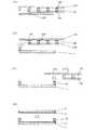
先ず、図3(a)の平面図や図3(b)の断面図に示すように、上下全面に接着層6Aと6Bが形成されると共に、この接着層6Aと6B上下全面に、紙やポリエチレンテレフタレート等の上剥離シート17Aと下剥離シート17Bが貼付され、上下端に所定間隔で通孔18Bが設けられた帯状のスペーサシート18に、下方から上剥離シート17Aを残してハーフカット加工を行う。 First, as shown in the plan view of FIG. 3A and the cross-sectional view of FIG. 3B,
そして、図3(a)に示すような、ハッチングされた略L字状の複数のスペーサ部18Aを形成した後、図3(c)の断面図に示すように、このスペーサ部18A以外の箇所のスペーサシート18や下剥離シート17Bを、上剥離シート17Aから剥離することによって、上剥離シート17A下面に、左右方向に配列された略L字状の複数のスペーサ15が形成される。 Then, after forming a plurality of hatched substantially L-
つまり、スペーサ15を略L字状とし、この複数のスペーサ15をスペーサシート18に所定方向に配列して形成することによって、図3(a)に示すように、複数のスペーサ15間の間隔を小さくでき、所定寸法のスペーサシート18から多くのスペーサ15を製作できるため、使用部材の無駄が少なく、使用効率を高めることが可能なように構成されている。 That is, the
なお、図3(a)では、構成を判り易くするために、複数のスペーサ15間の間隔を大きくし、隙間を比較的大きな状態で表しているが、上記のようにハーフカット加工によって複数のスペーサ15を形成する場合には、切断刃分の隙間だけを空け、もっと小さな間隔でさらに多くのスペーサ15を配列することが可能である。 In FIG. 3A, in order to make the configuration easy to understand, the interval between the plurality of
次に、図4(a)の断面図に示すように、例えば、左端に形成されたスペーサ15の下剥離シート17Bを剥離して下面の接着層6Bを露出させた後、図4(b)に示すように、配列されたスペーサ15が平行になるように、所定の組立治工具(図示せず)に保持された下基板1上面の、例えば左下外周に、このスペーサ15を貼付する。 Next, as shown in the sectional view of FIG. 4A, for example, the
なお、この時、下基板1を保持した組立治工具に突出ピン等を設け、これにスペーサシート18に所定間隔で設けられた通孔18Bを挿入して、下基板1上面にスペーサ15を貼付すれば、ズレ等がなく下基板1の正確な位置にスペーサ15を貼付することができる。 At this time, a protruding pin or the like is provided on the assembly jig holding the
また、この時、上剥離シート17A下面や下剥離シート17B上面に、接着層6Aや6Bとの剥離を容易にするために塗布されたシリコン等の種類や厚さを変え、上剥離シート17Aと下剥離シート17Bの剥離力を異なるものとすることによって、スペーサ15の貼付をより容易に行うことができる。 Further, at this time, the type and thickness of silicon applied on the lower surface of the
つまり、以上のように、先に下剥離シート17Bを剥離する場合には、下剥離シート17Bの剥離力を弱くし、上剥離シート17Aの剥離力を強くすることによって、図4(a)のように下剥離シート17Bを剥離する際、スペーサ15は剥離力の強い上剥離シート17Aに貼り付いたままで、剥離力の弱い下剥離シート17B側に付いて剥がれるというようなことがなく、下剥離シート17Bの剥離を容易に行うことができる。 That is, as described above, when the
そして、この後、図4(c)に示すように、スペーサシート18または下基板1を回転及び移動させ、次に配列されたスペーサ15の下剥離シート17Bを剥離した後、これを下基板1上面の右上外周に貼付する。 After that, as shown in FIG. 4C, the
最後に、図4(d)に示すように、下基板1上面に上基板2を上導電層4と下導電層3が対向するように重ね、下基板1と上基板2の外周を貼り合わすことによって、図1や図2に示したような、略L字状の二つのスペーサ15が上基板2と下基板1の間の対向する外周に貼付されたタッチパネルが完成する。 Finally, as shown in FIG. 4D, the upper substrate 2 is stacked on the upper surface of the
なお、二つのスペーサ15の間隙を封止するための封止材16の塗布や乾燥は、図4(c)の下基板1上面にスペーサ15を貼付した状態で行っても、完成したタッチパネルの状態で行ってもよい。 Even if the sealing
そして、このように構成されたタッチパネルは、液晶表示素子等の前面に配置されて電子機器に装着されると共に、一対の上電極と下電極が配線基板11の配線パターンを介して、機器の電子回路(図示せず)に接続される。 The touch panel configured in this manner is disposed on the front surface of a liquid crystal display element or the like and attached to an electronic device, and a pair of upper and lower electrodes are connected to the electronic device via the wiring pattern of the
以上の構成において、タッチパネル背面の液晶表示素子等の表示を視認しながら、上基板2上面を指或いはペン等で押圧操作すると、上基板2が撓み、押圧された箇所の上導電層4が下導電層3に接触する。 In the above configuration, when the upper surface of the upper substrate 2 is pressed with a finger or a pen while visually recognizing the display on the back surface of the touch panel, the upper substrate 2 is bent, and the upper conductive layer 4 at the pressed position is lowered. Contact the
そして、電子回路から上電極と下電極へ順次電圧が印加され、これらの電極間の電圧比によって、押圧された箇所を電子回路が検出し、機器の様々な機能の切換えが行われるように構成されている。 A voltage is sequentially applied from the electronic circuit to the upper electrode and the lower electrode, and the electronic circuit detects the pressed portion by the voltage ratio between these electrodes, and the various functions of the device are switched. Has been.
このように本実施の形態によれば、スペーサ15を略L字状とし、この複数のスペーサ15をスペーサシート18に所定方向に配列して形成することによって、所定寸法のスペーサシート18から多くのスペーサ15を製作できるため、使用部材の無駄が少なく、製作が容易で安価なタッチパネル及びその製造方法を得ることができるものである。 As described above, according to the present embodiment, the
また、略L字状の複数のスペーサ15の間隙を封止材16で封止することによって、下導電層3と上導電層4間の空隙への塵埃や水分の浸入を防止できるため、下導電層3と上導電層4の安定した接触を行うことができる。 In addition, by sealing the gaps between the plurality of substantially L-shaped
さらに、上剥離シート17Aと下剥離シート17Bの剥離力を異なるものとすることによって、上基板2や下基板1へのスペーサ15の貼付をより容易に行うことができる。 Furthermore, the
本発明によるタッチパネル及びその製造方法は、製作が容易で安価なものを提供することができるという有利な効果を有し、各種電子機器の操作用として有用である。 The touch panel and the manufacturing method thereof according to the present invention have an advantageous effect that it is easy to manufacture and can provide an inexpensive one, and are useful for operation of various electronic devices.
1 下基板
2 上基板
3 下導電層
4 上導電層
6A、6B 接着層
11 配線基板
15 スペーサ
16 封止材
17A 上剥離シート
17B 下剥離シート
18 スペーサシート
18A スペーサ部
18B 通孔DESCRIPTION OF
Claims (4)
Translated fromJapanesePriority Applications (3)
| Application Number | Priority Date | Filing Date | Title |
|---|---|---|---|
| JP2004255210AJP4539241B2 (en) | 2004-09-02 | 2004-09-02 | Touch panel and manufacturing method thereof |
| US11/191,798US7351922B2 (en) | 2004-09-02 | 2005-07-27 | Touch panel and the manufacturing method |
| CNB2005100958308ACN1322408C (en) | 2004-09-02 | 2005-09-02 | Touch panel and the manufacturing method |
Applications Claiming Priority (1)
| Application Number | Priority Date | Filing Date | Title |
|---|---|---|---|
| JP2004255210AJP4539241B2 (en) | 2004-09-02 | 2004-09-02 | Touch panel and manufacturing method thereof |
Publications (2)
| Publication Number | Publication Date |
|---|---|
| JP2006072693A JP2006072693A (en) | 2006-03-16 |
| JP4539241B2true JP4539241B2 (en) | 2010-09-08 |
Family
ID=35942392
Family Applications (1)
| Application Number | Title | Priority Date | Filing Date |
|---|---|---|---|
| JP2004255210AExpired - Fee RelatedJP4539241B2 (en) | 2004-09-02 | 2004-09-02 | Touch panel and manufacturing method thereof |
Country Status (3)
| Country | Link |
|---|---|
| US (1) | US7351922B2 (en) |
| JP (1) | JP4539241B2 (en) |
| CN (1) | CN1322408C (en) |
Families Citing this family (46)
| Publication number | Priority date | Publication date | Assignee | Title |
|---|---|---|---|---|
| EP1667183A1 (en)* | 2004-12-01 | 2006-06-07 | IEE INTERNATIONAL ELECTRONICS & ENGINEERING S.A. | Reinforced foil-type switching element |
| US20080185192A1 (en)* | 2007-02-06 | 2008-08-07 | Hsih Lung-Sheng | Touch panel |
| KR100984071B1 (en)* | 2007-03-30 | 2010-09-30 | 후지쯔 콤포넌트 가부시끼가이샤 | Touch panel |
| CN101470560B (en)* | 2007-12-27 | 2012-01-25 | 清华大学 | Touch screen and display equipment |
| CN101419518B (en)* | 2007-10-23 | 2012-06-20 | 清华大学 | Touch panel |
| CN101458600B (en)* | 2007-12-14 | 2011-11-30 | 清华大学 | Touch screen and display device |
| CN101458604B (en)* | 2007-12-12 | 2012-03-28 | 清华大学 | Touch screen and display device |
| CN101458595B (en)* | 2007-12-12 | 2011-06-08 | 清华大学 | Touch screen and display device |
| CN101620454A (en)* | 2008-07-04 | 2010-01-06 | 清华大学 | Potable computer |
| CN101458598B (en)* | 2007-12-14 | 2011-06-08 | 清华大学 | Touch screen and display device |
| CN101676832B (en)* | 2008-09-19 | 2012-03-28 | 清华大学 | Desktop PC |
| CN101655720B (en)* | 2008-08-22 | 2012-07-18 | 清华大学 | Personal digital assistant |
| CN101458608B (en)* | 2007-12-14 | 2011-09-28 | 清华大学 | Touch screen preparation method |
| CN101458609B (en)* | 2007-12-14 | 2011-11-09 | 清华大学 | Touch screen and display device |
| CN101458606B (en)* | 2007-12-12 | 2012-06-20 | 清华大学 | Touch screen, method for producing the touch screen, and display device using the touch screen |
| CN101458597B (en)* | 2007-12-14 | 2011-06-08 | 清华大学 | Touch screen, method for producing the touch screen, and display device using the touch screen |
| CN101458593B (en)* | 2007-12-12 | 2012-03-14 | 清华大学 | Touch screen and display device |
| CN101419519B (en)* | 2007-10-23 | 2012-06-20 | 清华大学 | Touch panel |
| CN101458605B (en)* | 2007-12-12 | 2011-03-30 | 鸿富锦精密工业(深圳)有限公司 | Touch screen and display device |
| CN101458594B (en)* | 2007-12-12 | 2012-07-18 | 清华大学 | Touch screen and display device |
| CN101458599B (en)* | 2007-12-14 | 2011-06-08 | 清华大学 | Touch screen, method for producing the touch screen, and display device using the touch screen |
| CN101458603B (en)* | 2007-12-12 | 2011-06-08 | 北京富纳特创新科技有限公司 | Touch screen and display device |
| CN101470566B (en)* | 2007-12-27 | 2011-06-08 | 清华大学 | Touch control device |
| CN101470559B (en)* | 2007-12-27 | 2012-11-21 | 清华大学 | Touch screen and display equipment |
| CN101458602B (en)* | 2007-12-12 | 2011-12-21 | 清华大学 | Touch screen and display device |
| CN101656769B (en)* | 2008-08-22 | 2012-10-10 | 清华大学 | Mobile telephone |
| CN101458596B (en)* | 2007-12-12 | 2011-06-08 | 北京富纳特创新科技有限公司 | Touch screen and display device |
| CN101470558B (en)* | 2007-12-27 | 2012-11-21 | 清华大学 | Touch screen and display equipment |
| CN101464763B (en)* | 2007-12-21 | 2010-09-29 | 清华大学 | Manufacturing method of touch screen |
| CN101458975B (en)* | 2007-12-12 | 2012-05-16 | 清华大学 | Electronic element |
| CN101458601B (en)* | 2007-12-14 | 2012-03-14 | 清华大学 | Touch screen and display device |
| CN101464757A (en)* | 2007-12-21 | 2009-06-24 | 清华大学 | Touch screen and display equipment |
| CN101458607B (en)* | 2007-12-14 | 2010-12-29 | 清华大学 | Touch screen and display device |
| CN101464766B (en)* | 2007-12-21 | 2011-11-30 | 清华大学 | Touch screen and display equipment |
| CN101470565B (en)* | 2007-12-27 | 2011-08-24 | 清华大学 | Touch screen and display device |
| CN101464765B (en)* | 2007-12-21 | 2011-01-05 | 鸿富锦精密工业(深圳)有限公司 | Touch screen and display equipment |
| CN101464764B (en)* | 2007-12-21 | 2012-07-18 | 清华大学 | Touch screen and display equipment |
| US8574393B2 (en)* | 2007-12-21 | 2013-11-05 | Tsinghua University | Method for making touch panel |
| CN101470564B (en)* | 2007-12-28 | 2011-06-08 | 财团法人工业技术研究院 | Touch panel and manufacturing method thereof |
| CN101620492B (en)* | 2008-07-04 | 2011-03-30 | 鸿富锦精密工业(深圳)有限公司 | Manufacturing method of touch screen |
| US8237677B2 (en)* | 2008-07-04 | 2012-08-07 | Tsinghua University | Liquid crystal display screen |
| US8390580B2 (en)* | 2008-07-09 | 2013-03-05 | Tsinghua University | Touch panel, liquid crystal display screen using the same, and methods for making the touch panel and the liquid crystal display screen |
| CN101924816B (en)* | 2009-06-12 | 2013-03-20 | 清华大学 | Flexible mobile phone |
| CN101770312B (en)* | 2010-03-02 | 2012-07-04 | 友达光电股份有限公司 | Touch control display panel |
| CN102673086B (en)* | 2012-05-10 | 2014-12-17 | 无锡博一光电科技有限公司 | Method for attaching touch panel and LCD panel |
| CN114126207B (en)* | 2020-08-27 | 2024-03-26 | 致伸科技股份有限公司 | Thin film circuit board and production method thereof |
Family Cites Families (14)
| Publication number | Priority date | Publication date | Assignee | Title |
|---|---|---|---|---|
| US4958148A (en)* | 1985-03-22 | 1990-09-18 | Elmwood Sensors, Inc. | Contrast enhancing transparent touch panel device |
| US4786767A (en)* | 1987-06-01 | 1988-11-22 | Southwall Technologies Inc. | Transparent touch panel switch |
| JPH02105916A (en)* | 1988-10-14 | 1990-04-18 | Canon Inc | touch panel input device |
| JP2545233Y2 (en)* | 1990-07-09 | 1997-08-25 | カシオ計算機株式会社 | Key input device |
| JPH0927243A (en)* | 1995-07-13 | 1997-01-28 | Hitachi Aic Inc | Touch screen |
| TW388894B (en)* | 1997-10-09 | 2000-05-01 | Nissha Printing | High strength touch panel and manufacturing method therefor |
| JP4596687B2 (en)* | 2000-07-27 | 2010-12-08 | 富士通コンポーネント株式会社 | PANEL TYPE PERIPHERAL DEVICE, ITS MANUFACTURING METHOD, AND PANEL JIG FOR MANUFACTURING THE SAME |
| US6587097B1 (en)* | 2000-11-28 | 2003-07-01 | 3M Innovative Properties Co. | Display system |
| JP2002202855A (en)* | 2000-12-28 | 2002-07-19 | Matsushita Electric Ind Co Ltd | Touch panel and electronic device using the same |
| JP4055378B2 (en)* | 2001-07-06 | 2008-03-05 | 松下電器産業株式会社 | Touch panel switch |
| TWI224276B (en)* | 2001-11-02 | 2004-11-21 | Matsushita Electric Industrial Co Ltd | Touch panel and method of manufacturing the same |
| JP4066641B2 (en)* | 2001-11-20 | 2008-03-26 | 松下電器産業株式会社 | Touch panel |
| JP2003280821A (en) | 2002-03-26 | 2003-10-02 | Matsushita Electric Ind Co Ltd | Light transmissive touch panel |
| JP3960850B2 (en)* | 2002-04-26 | 2007-08-15 | ホシデン株式会社 | Touch panel |
- 2004
- 2004-09-02JPJP2004255210Apatent/JP4539241B2/ennot_activeExpired - Fee Related
- 2005
- 2005-07-27USUS11/191,798patent/US7351922B2/ennot_activeExpired - Fee Related
- 2005-09-02CNCNB2005100958308Apatent/CN1322408C/ennot_activeExpired - Fee Related
Also Published As
| Publication number | Publication date |
|---|---|
| JP2006072693A (en) | 2006-03-16 |
| CN1322408C (en) | 2007-06-20 |
| US20060044284A1 (en) | 2006-03-02 |
| CN1744021A (en) | 2006-03-08 |
| US7351922B2 (en) | 2008-04-01 |
Similar Documents
| Publication | Publication Date | Title |
|---|---|---|
| JP4539241B2 (en) | Touch panel and manufacturing method thereof | |
| JP4711150B2 (en) | Touch panel and display device | |
| US8049127B2 (en) | Touch panel | |
| JP5194496B2 (en) | Touch panel | |
| JP4687561B2 (en) | Touch panel | |
| JP2012048279A (en) | Input device | |
| JP2008027016A (en) | Touch panel | |
| JP2011013881A (en) | Touch panel | |
| JP5531778B2 (en) | Touch panel | |
| JP2008027329A (en) | Touch panel | |
| JP4893082B2 (en) | Touch panel | |
| JP2007233513A (en) | Touch panel | |
| JP2007172025A (en) | Touch panel | |
| JP2009176199A (en) | Touch panel | |
| JP2014026496A (en) | Touch panel | |
| JP4487757B2 (en) | Touch panel | |
| JP2009104372A (en) | Wiring board and touch panel using the same | |
| JP2010191741A (en) | Touch panel | |
| JP2007140724A (en) | Touch panel and manufacturing method thereof | |
| JP2014035615A (en) | Touch panel | |
| JP2011065407A (en) | Touch panel | |
| JP5093018B2 (en) | Input device | |
| JP2007213302A (en) | Touch panel | |
| JP2014093010A (en) | Touch panel | |
| JP2010026670A (en) | Touch panel and manufacturing method therefor |
Legal Events
| Date | Code | Title | Description |
|---|---|---|---|
| A621 | Written request for application examination | Free format text:JAPANESE INTERMEDIATE CODE: A621 Effective date:20070614 | |
| RD01 | Notification of change of attorney | Free format text:JAPANESE INTERMEDIATE CODE: A7421 Effective date:20070712 | |
| RD01 | Notification of change of attorney | Free format text:JAPANESE INTERMEDIATE CODE: A7421 Effective date:20091120 | |
| A131 | Notification of reasons for refusal | Free format text:JAPANESE INTERMEDIATE CODE: A131 Effective date:20091208 | |
| A521 | Request for written amendment filed | Free format text:JAPANESE INTERMEDIATE CODE: A523 Effective date:20100208 | |
| TRDD | Decision of grant or rejection written | ||
| A01 | Written decision to grant a patent or to grant a registration (utility model) | Free format text:JAPANESE INTERMEDIATE CODE: A01 Effective date:20100601 | |
| A01 | Written decision to grant a patent or to grant a registration (utility model) | Free format text:JAPANESE INTERMEDIATE CODE: A01 | |
| A61 | First payment of annual fees (during grant procedure) | Free format text:JAPANESE INTERMEDIATE CODE: A61 Effective date:20100614 | |
| FPAY | Renewal fee payment (event date is renewal date of database) | Free format text:PAYMENT UNTIL: 20130702 Year of fee payment:3 | |
| LAPS | Cancellation because of no payment of annual fees |