JP4539112B2 - Method for manufacturing plasma display panel - Google Patents
Method for manufacturing plasma display panelDownload PDFInfo
- Publication number
- JP4539112B2 JP4539112B2JP2004047290AJP2004047290AJP4539112B2JP 4539112 B2JP4539112 B2JP 4539112B2JP 2004047290 AJP2004047290 AJP 2004047290AJP 2004047290 AJP2004047290 AJP 2004047290AJP 4539112 B2JP4539112 B2JP 4539112B2
- Authority
- JP
- Japan
- Prior art keywords
- exposure
- photomask
- pattern
- photosensitive
- exposure amount
- Prior art date
- Legal status (The legal status is an assumption and is not a legal conclusion. Google has not performed a legal analysis and makes no representation as to the accuracy of the status listed.)
- Expired - Fee Related
Links
Images


Landscapes
- Gas-Filled Discharge Tubes (AREA)
Description
Translated fromJapanese本発明は、大画面で、薄型、軽量のディスプレイ装置として知られるプラズマディスプレイパネル(以下、PDPと記す)の構造物の形成を行うPDPの製造方法に関する。The present invention is a large-screen, flat-panel, plasma display panel, known as lightweight display device (hereinafter, referred to as PDP) aboutthe PDP manufacturing method of performing the formation of structures.
PDPは、液晶パネルに比べて高速の表示を行うことが可能である。また、視野角が広いこと、大型化が容易であること、さらには自発光型であるため表示品質が高いことなどの理由から、フラットパネルディスプレイの中でも注目されてきている。特に、多くの人が集まる公共の場所での表示装置や家庭で大画面の映像を楽しむための表示装置として各種の用途に多く使用されている。 The PDP can display at a higher speed than the liquid crystal panel. In addition, it has been attracting attention among flat panel displays because of its wide viewing angle, easy enlargement, and high display quality due to its self-luminous type. In particular, it is widely used in various applications as a display device in a public place where many people gather and a display device for enjoying a large screen image at home.
PDPは、ガス放電により紫外線を発生させ、この紫外線で蛍光体を励起して発光させることにより画像表示を行うもので、駆動方式は、大別して、AC型とDC型とに分かれる。また、放電方式は面放電型と対向放電型とに分けられる。昨今では、高精細化、大画面化及び構造の簡素性に伴う製造の簡便性から、3電極構造の面放電型のPDPが主流になってきている。 The PDP generates an ultraviolet ray by gas discharge and performs image display by exciting a phosphor with the ultraviolet ray to emit light, and the driving system is roughly divided into an AC type and a DC type. Further, the discharge method is classified into a surface discharge type and a counter discharge type. In recent years, a surface discharge type PDP having a three-electrode structure has become the mainstream because of the simplicity of manufacturing accompanying high definition, large screen, and simple structure.
この構造は、ガラス等の基板上に、走査電極と維持電極とからなる表示電極と、それを覆う誘電体層と、さらにそれを覆う保護層とを有する前面板と、表示電極に対して直交する複数のアドレス電極と、それを覆う誘電体層と、誘電体層上の隔壁とを有する背面板とを対向配置させることにより、表示電極とデータ電極との交差部に放電セルを形成し、且つ放電セル内に蛍光体層を備えたものである。 In this structure, a front plate having a display electrode composed of a scan electrode and a sustain electrode on a substrate such as glass, a dielectric layer covering the display electrode, and a protective layer covering the display electrode, and orthogonal to the display electrode Forming a discharge cell at the intersection of the display electrode and the data electrode by opposingly arranging a plurality of address electrodes, a dielectric layer covering the address electrode, and a back plate having a partition wall on the dielectric layer, In addition, a phosphor layer is provided in the discharge cell.
このPDPにおいては、例えば、表示電極やアドレス電極などに対しては、その形状及び配設ピッチに高精度が要求される。このため、例えば、金属材料等のような導電性材料に、感光性材料を含有させた材料を基板全面に塗布し、それを電極パターンを備えたフォトマスクにより露光、現像するという、いわゆるフォトリソグラフィ法が採用されている(例えば、非特許文献1参考)。
感光性材料は露光により架橋反応し、硬化するのであるが、その露光の条件次第では露光が過露光となってしまう場合がある。そのような場合には架橋反応が過度に進行してしまい、電極膜には応力が内在した状態となり、このような状態で焼成を行うと電極膜が収縮し、例えば、電極のパターン形状におけるエッジ部で、反り上がりや剥がれといった問題が発生する場合がある。 The photosensitive material undergoes a crosslinking reaction upon exposure and cures, but depending on the exposure conditions, the exposure may be overexposed. In such a case, the cross-linking reaction proceeds excessively, and the electrode film is in a state where stress is inherent. When firing in such a state, the electrode film contracts, for example, an edge in the pattern shape of the electrode In some cases, problems such as warping and peeling may occur.
以上は電極の例であるが、PDPにおいては、大画面であるにも関わらずその構造物には精度を要求されている。したがって、電極以外の、例えば隔壁などの形成にも、同様にフォトリソグラフィ法が用いられる場合があり、そのような場合にも、上記と同様、画像表示に支障が生じる場合がある。このような問題が発生すると、表示する画像に対して悪影響を与えることとなる。 The above is an example of an electrode. However, in the PDP, the structure is required to have precision despite the large screen. Therefore, the photolithographic method may be used in the same manner for forming other than the electrodes, for example, barrier ribs. In such a case, the image display may be hindered as described above. When such a problem occurs, the displayed image is adversely affected.
本発明は上述した問題を解決するためになされたものであり、PDPの構造物の形成をフォトリソグラフィ法により行う際、形成した構造物の反り上がり、剥がれなどを抑制することができるPDPの製造方法およびPDPを提供することを目的とする。 The present invention has been made to solve the above-described problems. When a PDP structure is formed by a photolithography method, the manufacturing of the PDP that can suppress warping and peeling of the formed structure is provided. An object is to provide a method and a PDP.
上記目的を達成するために本発明のPDPの製造方法は、ガラスフリットを含有し露光による架橋反応によって硬化する感光性材料を塗布する工程と、その後、この塗布した感光性材料を所定のパターンに露光する工程と、その後、この露光した感光性材料を現像する工程と、その後、この現像した感光性材料を焼成する工程と、により、前記感光性材料を所定のパターンにパターニングすることでPDPの構造物の形成を行うPDPの製造方法であって、前記所定のパターンに露光する工程を、露光部のパターンが同一で開口幅が異なる二つのフォトマスクを用い、開口幅の広いフォトマスクによるパターン露光の際の露光量を、必要な全露光量の2/3程度とし、開口幅の狭いフォトマスクによるパターン露光の際の露光量は、必要な全露光量の1/3程度とする、2回の露光に別けて行う、というものである。In order to achieve the above object, a method for producing a PDP of the present invention comprisesa step of applying a photosensitive material containing glass frit and cured by a crosslinking reaction by exposure, and then applying the applied photosensitive material into a predetermined pattern. The PDP is patterned by patterning the photosensitive material into a predetermined pattern by an exposure step, a step of developing the exposed photosensitive material, and a step of baking the developed photosensitive material. A method of manufacturing a PDP for forming a structure, wherein the step of exposing the predetermined pattern is performed by using two photomasks having the same exposed portion pattern and different opening widths, and using a photomask having a wide opening width. The exposure amount at the time of exposure is about 2/3 of the required total exposure amount, and the exposure amount at the time of pattern exposure with a photomask having a narrow aperture width is the total required exposure amount. And about one third of the amount of light is carried out divided into two exposures, is that.
本発明によれば、PDPの構造物の形成をフォトリソグラフィ法により行う際、形成した構造物の反り上がり、剥がれなどを抑制することができるPDPの製造方法およびPDPを提供することが可能となる。 ADVANTAGE OF THE INVENTION According to this invention, when forming the structure of PDP by the photolithographic method, it becomes possible to provide the manufacturing method of PDP and PDP which can suppress a warp rise, peeling, etc. of the formed structure. .
すなわち、本発明の請求項1に記載の発明は、ガラスフリットを含有し露光による架橋反応によって硬化する感光性材料を塗布する工程と、その後、この塗布した感光性材料を所定のパターンに露光する工程と、その後、この露光した感光性材料を現像する工程と、その後、この現像した感光性材料を焼成する工程と、により、前記感光性材料を所定のパターンにパターニングすることでプラズマディスプレイパネルの構造物の形成を行うプラズマディスプレイパネルの製造方法であって、前記所定のパターンに露光する工程を、露光部のパターンが同一で開口幅が異なる二つのフォトマスクを用い、開口幅の広いフォトマスクによるパターン露光の際の露光量を、必要な全露光量の2/3程度とし、開口幅の狭いフォトマスクによるパターン露光の際の露光量は、必要な全露光量の1/3程度とする、2回の露光に別けて行う、プラズマディスプレイパネルの製造方法である。That is, the invention described in
以下、本発明の一実施の形態に係るPDPの製造方法について、図を用いて以下に説明する。 Hereinafter, the manufacturing method of PDP which concerns on one embodiment of this invention is demonstrated below using figures.
(実施の形態1)
まず、PDPの構造の一例について説明する。図1は、本発明の一実施の形態に係るPDPの製造方法によって製造される、PDPの概略構成の一例を示す断面斜視図である。(Embodiment 1)
First, an example of the structure of the PDP will be described. FIG. 1 is a cross-sectional perspective view showing an example of a schematic configuration of a PDP manufactured by a method for manufacturing a PDP according to an embodiment of the present invention.
PDP1の前面板2は、例えばフロート法により得られたガラスのような、平滑、透明且つ絶縁性を備えた基板3の一主面上に形成された、走査電極4と維持電極5とからなる表示電極6を有する。また表示電極6と、それに隣接する他の表示電極6との間に設けた遮光層7と、表示電極6と遮光層7とを覆う誘電体層8と、さらにその誘電体層8を覆う、例えばMgOを含む保護層9とを有する。 The front plate 2 of the
走査電極4と維持電極5は、電気抵抗の低減を図るために、透明電極4a及び5aに金属材料のような良導電性材料によるバス電極4b及び5bをそれぞれ積層した構造としている。また、遮光層7は、非発光時に蛍光体層(後述)からの白色を遮蔽し、コントラストを向上させるために効果的である。 Scan electrode 4 and sustain electrode 5 have a structure in which
背面板10は、背面側の、例えばフロート法により得られたガラスのような、平滑、且つ絶縁性を備えた基板11の一主面上に形成したアドレス電極12と、そのアドレス電極12を覆う誘電体層13と、誘電体層13上の、隣り合うアドレス電極12の間に相当する場所に配置される隔壁14と、その隣の他の隔壁14との間の蛍光体層15R、15G及び蛍光体層15Bとを有する。 The
前面板2と背面板10とは、隔壁14を挟んで、表示電極6とアドレス電極12とが直交するように対向配置し、前面板2と背面板10の周囲を封着部材により封止した構成である。前面板2と背面板10との間に形成された放電空間16には、例えばNe−Xe5%の放電ガスを66.5kPa(500Torr)の圧力で封入する。 The front plate 2 and the
そして、放電空間16の表示電極6とアドレス電極12との交差部が放電セル17(単位発光領域)として動作する。 The intersection between the display electrode 6 and the
次に、PDP1について、その製造方法を図1を参照しながら説明する。 Next, a manufacturing method of the
前面板2を製造するに当たっては、まず基板3の上に、走査電極4及び維持電極5を例えばストライプ状に形成する。具体的には、基板3の上に透明電極4a、5aの材料である例えばITOによる膜を、例えば電子ビーム蒸着法により形成する。さらにそのITO膜の上にレジストを、透明電極4a、5aのパターンとして残るようにパターニングを行う。そしてこの状態で透明電極4a、5aをエッチングし、その後、レジストを剥離して、ストライプ状に透明電極4a、5aを形成する。なお、透明電極材料としてはSnO2等も用いることができる。In manufacturing the front plate 2, first, the scan electrodes 4 and the sustain electrodes 5 are formed on the
そして、透明電極4a、5aの上にバス電極4b、5bを形成する。バス電極4b、5bの材料としては、黒色顔料、ガラスフリット(PbO−B2O3−SiO2系やBi2O3−B2O3−SiO2系等)、重合開始剤、光硬化性モノマー、有機溶剤を含む感光性黒色ペーストを用いる。Then,
そして、この感光性黒色ペーストをスクリーン印刷法等によりガラス基板上に黒色電極膜を成膜した後、乾燥させ、引き続き、スクリーン印刷法等により黒色電極膜の上にAgを材料に含有する導電性材料、ガラスフリット(PbO−B2O3−SiO2系やBi2O3−B2O3−SiO2系等)、重合開始剤、光硬化性モノマー、有機溶剤を含む感光性Agペーストを用いて金属電極膜を成膜し、再度、乾燥する。その後、フォトリソグラフィ法によってパターニングし、焼成してバス電極4b、5bを形成する。Then, after forming a black electrode film on the glass substrate by a screen printing method or the like, this photosensitive black paste is dried, and subsequently, a conductive material containing Ag as a material on the black electrode film by a screen printing method or the like. Photosensitive Ag paste containing materials, glass frit (PbO—B2 O3 —SiO2 system, Bi2 O3 —B2 O3 —SiO2 system, etc.), polymerization initiator, photocurable monomer, organic solvent A metal electrode film is formed by using, and dried again. Thereafter, patterning is performed by a photolithography method and baking is performed to form
上述の製造方法により、走査電極4及び維持電極5からなる表示電極6を形成することができる。 The display electrode 6 including the scan electrode 4 and the sustain electrode 5 can be formed by the manufacturing method described above.
次に、遮光層7を形成する。これは、感光性黒色ペーストをスクリーン印刷法等により成膜した後、フォトリソグラフィ法によってパターニングし、焼成して形成する。なお、遮光層7は、バス電極4b、5bの下地黒色層と同時に形成しても良い。また、感光性ペーストが黒色であればペーストを用いた形成方法でなくとも良い。なお、遮光層7は、バス電極4b、5b形成の前に形成しても良い。 Next, the
次に、表示電極6と遮光層7とを、誘電体層8で被覆する。誘電体層8は、鉛系のガラス材料を含むペーストを例えばスクリーン印刷で塗布して形成する。その後、所定温度で所定時間、例えば560℃で20分間、ペーストを焼成することによって、誘電体層8は所定の厚み、たとえば約20μmの厚みに形成される。 Next, the display electrode 6 and the
鉛系のガラス材料を含むペーストとしては、例えば、PbO(70wt%)、B2O3(15wt%)、SiO2(10wt%)、及びAl2O3(5wt%)と有機バインダ(例えば、α−ターピネオールに10%のエチルセルローズを溶解したもの)との混合物が使用される。ここで、有機バインダとは樹脂を有機溶媒に溶解したものであり、エチルセルローズ以外に樹脂としてアクリル樹脂、有機溶媒としてブチルカービトールなども使用することができる。Examples of the paste containing a lead-based glass material include PbO (70 wt%), B2 O3 (15 wt%), SiO2 (10 wt%), and Al2 O3 (5 wt%) and an organic binder (for example, a mixture of 10% ethyl cellulose in α-terpineol). Here, the organic binder is obtained by dissolving a resin in an organic solvent. In addition to ethyl cellulose, an acrylic resin can be used as the resin, and butyl carbitol can be used as the organic solvent.
さらに、こうした有機バインダに分散剤、例えば、グリセルトリオレエートを混入させても良い。また、ペーストを用いてスクリーン印刷する代わりに、成型されたフィルム状の誘電体前駆体をラミネートして焼成することによって形成しても良い。 Further, a dispersant such as glyceryl trioleate may be mixed in such an organic binder. Further, instead of screen printing using a paste, a molded film-like dielectric precursor may be laminated and fired.
次に、誘電体層8を保護層9で被覆する。保護層9は、例えばMgOを主成分とするものである。蒸着やスパッタなどの成膜プロセスにより、保護層9が所定の厚み、たとえば約0.5μmになるように形成する。 Next, the
一方、背面板10は、基板11上に、アドレス電極12をストライプ状に形成する。具体的には、基板11上に、アドレス電極12の材料となる、例えば感光性Agペーストを用い、スクリーン印刷法等により膜を形成し、その後、フォトリソグラフィ法などによってパターニングし、焼成して形成する。 On the other hand, the
次に、アドレス電極12を、誘電体層13により被覆する。誘電体層13は、例えば、鉛系のガラス材料を含むペーストを、例えば、スクリーン印刷で塗布した後、所定温度で所定時間、例えば560℃で20分間焼成する。これによって、誘電体層13は約20μmの所定の厚みに形成される。 Next, the
また、ペーストをスクリーン印刷する代わりに、成型されたフィルム状の下地誘電体層前駆体をラミネートして焼成することによって形成しても良い。 Further, instead of screen-printing the paste, it may be formed by laminating and firing a molded film-like base dielectric layer precursor.
次に、隔壁14を例えばストライプ状に形成する。隔壁14は、Al2O3等の骨材とガラスフリットとを主剤とする感光性ペーストを印刷法やダイコート法等により成膜し、フォトリソグラフィ法によりパターニングし、焼成して形成する。または、例えば、鉛系のガラス材料を含むペーストを、例えば、スクリーン印刷法により所定のピッチで繰り返し塗布した後、焼成することによって形成しても良い。ここで、隔壁14の間隙の寸法は、例えば32インチ〜50インチのHD−TVの場合、130μm〜240μm程度である。Next, the
そして、隔壁14と、隣の隔壁14との間の溝には、赤色(R)、緑色(G)及び青色(B)の各蛍光体粒子により構成される蛍光体層15R、15G及び15Bを形成する。これは、各色の蛍光体粒子と有機バインダとからなるペースト状の蛍光体インキを塗布し、これを例えば、400〜590℃の温度で焼成して有機バインダを焼失させる。これによって、各蛍光体粒子が結着してなる蛍光体層15R、15G及び15Bが形成される。 And in the groove | channel between the
前面板2と背面板10とを、前面板2の表示電極6と背面板10のアドレス電極12とが直交するように重ね合わせるとともに、前面板2と背面板10との周縁に封着用ガラス等の封着部材を介挿し、これを例えば450℃程度で10〜20分間焼成して形成した気密シール層(図示せず)により封着する。そして、一旦、放電空間16内を高真空、例えば、1.1×10⁻⁴Paで排気したのち、放電ガス(例えば、He−Xe系、Ne−Xe系の不活性ガス)を所定の圧力で封入することによってPDP1を作製する。The front plate 2 and the
ここで、PDP1は大画面であると同時に、表示電極6、遮光層7、アドレス電極12、隔壁14などの、PDP1の構造物には形状及び位置に対する精度が要求されるため、これらPDP1の構造物の形成方法としては、フォトリソグラフィ法が多く用いられている。 Here, since the
そこで、本発明に係るPDPの製造方法におけるフォトリソグラフィ法について、PDPの一構造物であるアドレス電極12の形成を例として、本発明の特徴的な点である、露光工程の流れを中心に、図を用いて説明する。 Therefore, with respect to the photolithography method in the PDP manufacturing method according to the present invention, focusing on the flow of the exposure process, which is a characteristic point of the present invention, taking as an example the formation of the
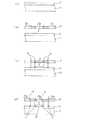
図2は、アドレス電極12を形成する際の工程の概略の流れを示す図である。 FIG. 2 is a diagram showing a schematic flow of steps in forming the
まず図2(a)に示すように、基板11上に、スクリーン印刷法等により感光性Agペースト均一に塗布することで感光性Agペースト膜21を形成する。Agペースト膜21は図1に示したアドレス電極12の前駆体となる。 First, as shown in FIG. 2A, the photosensitive
次に、図2(b)に示すように、フォトリソグラフィ法によりアドレス電極12を得るための露光パターンを備えるフォトマスク22を、基板11上の所定の位置に位置合わせして配置する。図2(b)においては、第1のフォトマスク22のハッチングのない部分が開口幅Aの開口部であり露光部22aとなる。 Next, as shown in FIG. 2B, a
次に、図2(c)に示すように、フォトマスク22を介して、感光性Agペースト膜21に対して1回目の露光を行う。具体的には、超高圧水銀ランプによる紫外線23(境界となる箇所に対して表示している)を照射する。 Next, as shown in FIG. 2C, the photosensitive
次に、図2(d)に示すように、フォトリソグラフィ法によりアドレス電極12を得るための露光パターンで、第1のフォトマスク22と同一のパターンであるがその開口部の開口幅Bが異なる露光パターンを備える第2のフォトマスク24を、所定の位置に位置合わせして設置する。図2(d)では、第2のフォトマスク24におけるハッチングのない部分が開口幅Bの開口部であり露光部24aとなる。 Next, as shown in FIG. 2D, the exposure pattern for obtaining the
そして以上のようにしてアドレス電極12のパターンを露光した感光性Agペースト膜21に対して、現像を行うことで、感光性Agペースト膜21をアドレス電極12のパターンとし、それを焼成することでアドレス電極12を形成する。 Then, by developing the photosensitive
ここで、第1のフォトマスク22の開口幅Aと第2のフォトマスク24の開口幅Bとは、その位置合わせの誤差による、1回目の露光と2回目の露光とにより露光される領域の位置ずれによる線幅の変化を抑制するために、以下の関係を有するものとする。すなわち、どちらか一方のフォトマスク、例えば第1のフォトマスク22の開口幅Aは、アドレス電極12のパターンを形成するための所定の開口幅とする。そしてもう一方のフォトマスクである第2のフォトマスク24の開口幅Bは、第1のフォトマスク22と同一の露光パターンであるが、第1のフォトマスク22の開口幅Aよりも、狭くした開口幅Bとしている。 Here, the opening width A of the
そして、第1のフォトマスク22による1回目の露光による露光領域内に、2回目の露光領域が収まるように、第2のフォトマスク24を位置合わせして露光を行う。ここで、第1のフォトマスク22の露光部22aの開口幅Aに対して狭くした、第2のフォトマスク24の露光部24aの開口幅Bの大きさは、露光パターンのデザイン、各フォトマスクの位置決め精度、及び感光性材料の焼成時の収縮率などの材料特性、等に基づき決定すればよい。 Then, exposure is performed by aligning the
さらに、上述の露光においては、1回目の露光と2回目の露光とで露光量を異ならせるようにする。具体的には、開口幅の広い方のフォトマスク、すなわち上述の例では第1のフォトマスク22による露光の際の露光量を、開口幅の狭い方のフォトマスク、すなわち上述の例では第2のフォトマスク24による露光の際の露光量より大きくする。さらに具体的には、例えば、第1のフォトマスク22による露光の際の露光量を、感光性Agペースト膜21の露光に必要とされる露光量の2/3程度とし、また、第2のフォトマスク24による露光の際の露光量は、感光性Agペースト膜21の露光に必要とされる露光量の1/3程度となるようにし、1回目の露光と2回目の露光との合計の露光量が感光性Agペースト膜21の露光に必要とされる露光量を超えないようにする。 Further, in the above-described exposure, the exposure amount is different between the first exposure and the second exposure. Specifically, the exposure amount at the time of exposure with the photomask having the wider opening width, that is, the
上述のような露光工程によれば、感光性Agペースト膜21においては、露光の履歴として図2(d)に示すように、1回目と2回目との両方の露光を受けた領域B'(第2のフォトマスク24の露光部24aを通して露光された領域)と、1回目の露光のみを受けた領域C'(第1のフォトマスク22の露光部22aを通して露光された領域A'から領域B'を除いた領域)とに分かれる。そして、露光パターンのエッジ部は、1回だけ露光される領域C'となることから、エッジ部が過露光となることは抑制されることとなり、過露光により発生する応力が原因となるパターンのエッジ部での反り上がりや剥がれといった問題の発生を抑制することが可能となる。 According to the exposure process as described above, in the photosensitive
ここで、上述の例においては、露光パターンのエッジ部における露光量は、直接的には、必要とされる露光量の2/3程度である。そして、露光量が不足していると、露光時の光照射は膜表面から行われ架橋反応は膜表面から進行するため、電極膜表面では硬化が十分に行われているが電極膜内部では硬化が不充分な状態となる。このような場合も、露光パターンに剥がれ等が発生しやすくなる。 Here, in the above-described example, the exposure amount at the edge portion of the exposure pattern is directly about 2/3 of the required exposure amount. If the exposure amount is insufficient, light irradiation at the time of exposure is performed from the film surface and the crosslinking reaction proceeds from the film surface. Therefore, the electrode film surface is sufficiently cured but is cured inside the electrode film. Is insufficient. Even in such a case, the exposure pattern easily peels off.
しかしながら、上述した露光工程においては、露光パターンに剥がれ等が発生するという不都合が生じることが非常に稀であることを実験的に確認している。これは、以下の理由によるものであると考えられる。 However, in the above-described exposure process, it has been experimentally confirmed that it is very rare that an inconvenience such as peeling occurs in the exposure pattern. This is considered to be due to the following reason.
すなわち架橋反応は、露光の際、膜厚方向のみではなく面方向にも拡がる。したがって、2回目の露光の際、露光パターンのエッジ部(領域C')には直接露光されなくても、その膜面方向に拡がる架橋反応により、実際には、架橋反応は進行しているものと考えられる。このことにより、必要とされる所定の露光量とまではならないまでも、パターン形成上、問題となるような露光不足には至らないものと考えられる。 That is, the crosslinking reaction extends not only in the film thickness direction but also in the surface direction during exposure. Therefore, in the second exposure, even if the edge portion (region C ′) of the exposure pattern is not directly exposed, the crosslinking reaction actually proceeds due to the crosslinking reaction spreading in the film surface direction. it is conceivable that. Thus, even if the required exposure amount is not reached, it is considered that the shortage of exposure that causes a problem in pattern formation does not occur.
また、上述では、先に開口幅が大きな方のフォトマスクで1回目の露光量の多い露光を行い、引き続き、開口幅が小さな方のフォトマスクで、2回目の露光量の少ない方の露光を行うという手順を示した。しかし、この手順を入れ替えて、先に開口幅が小さな方のフォトマスクを用いて1回目の、露光量の少ない露光を行い、引き続き、開口幅が大きな方のフォトマスクを用いて2回目の、露光量の多い露光を行うという形態の露光工程でも同様の効果を得ることができる。 In the above, the exposure with the first exposure amount is performed with the photomask having the larger opening width, and the exposure with the smaller exposure amount is performed with the photomask having the smaller opening width. The procedure to do was shown. However, by replacing this procedure, the first exposure with a smaller exposure amount is performed using a photomask having a smaller opening width, and then the second exposure is performed using a photomask having a larger opening width. The same effect can be obtained even in an exposure process in which exposure with a large exposure amount is performed.
上述したような本願発明の一実施の形態によるPDPの製造方法よれば、過露光、露光不足といった問題の発生を抑制した状態で感光性Agペースト膜21に対するパターン露光を良好に行うことが可能となる。 According to the method of manufacturing a PDP according to the embodiment of the present invention as described above, it is possible to satisfactorily perform pattern exposure on the photosensitive
なお、以上の説明においては、PDP1の構造物としてアドレス電極を例としたが、表示電極6、遮光層7、隔壁14など、フォトリソグラフィ法を用いて形成されるPDP1の構造物の少なくとも一つに対して適用することで同様の効果を得ることができる。 In the above description, the address electrode is taken as an example of the
(実施の形態2)
図3は、アドレス電極12を形成する際の工程の別の例の概略の流れを示す図である。(Embodiment 2)
FIG. 3 is a diagram showing a schematic flow of another example of a process for forming the
まず図3(a)に示すように、基板11上に、スクリーン印刷法等により感光性Agペースト均一に塗布して、感光性Agペースト膜21を形成する。 First, as shown in FIG. 3A, a photosensitive
次に図3(b)に示すように、フォトリソグラフィ法によりアドレス電極12を得るための露光パターンを備えるフォトマスク22を、基板11上の所定の位置に位置合わせして配置する。図3(b)においては、第1のフォトマスク22のハッチングのない部分が開口幅Aの開口部であり露光部22aとなる。 Next, as shown in FIG. 3B, a
次に、図3(c)に示すように、フォトマスク22を介して、感光性Agペースト膜21に対して1回目の露光を行う。具体的には、超高圧水銀ランプによる紫外線23(境界となる箇所に対して表示している)を照射する。 Next, as shown in FIG. 3C, the photosensitive
次に、図3(d)に示すように、フォトリソグラフィ法によりアドレス電極12を得るための露光パターンであって、第1のフォトマスク22と同一のパターンであるがその開口部の開口幅Bが異なる露光パターンを備える第2のフォトマスク24を、所定の位置に位置合わせして設置する。図3(d)では、第2のフォトマスク24におけるハッチングのない部分が開口幅Bの開口部であり露光部24aとなる。 Next, as shown in FIG. 3D, an exposure pattern for obtaining the
ここで、第1のフォトマスク22の開口幅Aと第2のフォトマスク24の開口幅Bとは、その位置合わせの誤差による、1回目の露光と2回目の露光とにより露光される領域の位置ずれによる線幅の変化を抑制するために、以下の関係を有するものとする。すなわち、どちらか一方のフォトマスク、例えば第1のフォトマスク22の開口幅Aは、アドレス電極12のパターンを形成するための所定の開口幅とする。そしてもう一方のフォトマスクである第2のフォトマスク24の開口幅Bは、第1のフォトマスク22と同一の露光パターンであるが、第1のフォトマスク22の開口幅Aよりも、狭くした開口幅Bとしている。 Here, the opening width A of the
そして、第1のフォトマスク22による1回目の露光による露光領域内に、2回目の露光領域が収まるように、第2のフォトマスク24を位置合わせして露光を行う。ここで、第1のフォトマスク22の露光部22aの開口幅Aに対して狭くした、第2のフォトマスク24の露光部24aの開口幅Bの大きさは、露光パターンのデザイン、各フォトマスクの位置決め精度、及び感光性材料の焼成時の収縮率などの材料特性、等に基づき決定すればよい。 Then, exposure is performed by aligning the
さらに、上述の露光においては、1回目の露光と2回目の露光とで露光量を異ならせるようにする。具体的には、開口幅の広い方のフォトマスク、すなわち上述の例では第1のフォトマスク22による露光の際の露光量を、開口幅の狭い方のフォトマスク、すなわち上述の例では第2のフォトマスク24による露光の際の露光量より大きくする。さらに具体的には、例えば、第1のフォトマスク22による露光の際の露光量を、感光性Agペースト膜21の露光に必要とされる露光量の2/3程度とし、また、第2のフォトマスク24による露光の際の露光量は、感光性Agペースト膜21の露光に必要とされる露光量の1/3程度となるようにし、1回目の露光と2回目の露光との合計の露光量が感光性Agペースト膜21の露光に必要とされる露光量を超えないようにする。 Further, in the above-described exposure, the exposure amount is different between the first exposure and the second exposure. Specifically, the exposure amount at the time of exposure with the photomask having the wider opening width, that is, the
上述のような露光工程により、実施の形態1で説明したように、過露光、露光不足といった問題の発生を抑制した状態で感光性Agペースト膜21に対するパターン露光を行うことが可能となるが、さらに、図3に示すように、第1のフォトマスク22の一部にダスト22bが付着し、また第2のフォトマスク24の一部にダスト24bが付着した状態となってしまった場合であっても、その影響を極めて小さいものとすることができる。 As described in the first embodiment, it is possible to perform pattern exposure on the photosensitive
すなわち、図3(c)に示すように、フォトマスク22を介して、感光性Agペースト膜21に対して1回目の露光を行う際、フォトマスク22の開口部22aにダスト22bが付着していると、感光性Agペースト膜21は、第1のフォトマスク22の露光部22aを通して露光される領域A'からダスト22bに対応する領域21aを除いた領域が実際に露光、感光されることとなる。 That is, as shown in FIG. 3C, when the photosensitive
次に、図3(d)に示すように、第2のフォトマスク24にダスト24bが付着しているとしても、それは第1のフォトマスク22に付着していたダスト22bと同一の箇所となる確率は非常に小さいものと考えられる。 Next, as shown in FIG. 3D, even if the
したがって、2回目の露光の際にダスト24bによって感光しない領域21bは、1回目の露光の際にダスト22bによって感光しなかった領域21aとは異なる領域となる可能性が非常に高くなる。すなわち、第1のフォトマスク22にダスト22bが付着していることで、1回目の露光においてダスト22bに対応する領域21aが感光しなくても、第2のフォトマスク24を用いた2回目の露光の際には、領域21aは感光する可能性が非常に高い。また、2回目の露光の際、ダスト24bにより露光が遮られ感光しなかった領域21bは、すでに1回目の露光により感光している可能性が非常に高い。 Therefore, the
以上説明したように、上述の例では露光を複数のフォトマスク毎に行っており、感光性Agペースト膜21に対してフォトマスクの交換によってでも同じ箇所にダストが位置するという確率は非常に小さいので、フォトマスクに付着したダストにより露光が全く遮られ全くの未感光となるという領域をほとんどなくすことが可能となる。 As described above, in the above-described example, the exposure is performed for each of the plurality of photomasks, and the probability that dust is located at the same position with respect to the photosensitive
ここで、上述の例においても、開口幅の広い方のフォトマスク、すなわち上述の例では第1のフォトマスク22での露光の露光量が、開口幅の狭い方のフォトマスク、すなわち上述の例では第2のフォトマスク24での露光の露光量より大きくしており、さらに具体的には、例えば、第1のフォトマスク22による露光の露光量を、感光性Agペースト膜21の露光に必要とされる露光量の2/3程度とし、また、第2のフォトマスク24による露光の露光量は、感光性Agペースト膜21の露光に必要とされる露光量の1/3程度となるようにし、1回目の露光と2回目の露光との合計の露光量が感光性Agペースト膜21の露光に必要とされる露光量を超えないようにしている。 Here, also in the above-described example, the exposure amount of the photomask having the wider opening width, that is, the photomask having the smaller opening width in the above-described example, that is, the photomask having the smaller opening width, that is, the above-described example. The exposure amount of the
このことから、1回目の露光の際、未露光領域となった、領域21aの露光量は、直接的には、感光性Agペースト膜21の露光に必要とされる露光量の1/3程度しか露光されないこととなる。また、2回目の露光の際、未露光領域となった、領域21bの露光量は、直接的には、感光性Agペースト膜21の露光に必要とされる露光量の2/3程度しか露光されないこととなる。しかしこのような場合にも、いずれも剥がれ等が発生する程度の露光不足となることがないことを実験的に確認している。 From this, the exposure amount of the
これも、架橋反応は、露光に対して、膜厚方向のみではなく面方向にも広がることから、例えば、領域21aは、1回目の露光の際に直接露光されなくてもその領域21aの周囲に対する露光によって、領域21aの部分にも架橋反応は進行しているものと考えられ、したがって、そのような状態で進行する架橋反応と、2回目の露光での、直接、露光されることにより進行する架橋反応との合算により、必要とされる所定の露光量とはならないまでも、パターン形成上、問題となるような露光不足には至らないものと考えられる。領域21bに対しても同様の理由で、必要とされる所定の露光量とはならないまでも、パターン形成上、問題となるような露光不足には至らないものと考えられる。 Again, since the crosslinking reaction spreads not only in the film thickness direction but also in the surface direction with respect to exposure, for example, even if the
以上のように、本願発明の一実施の形態によるPDPの製造方法よれば、フォトマスクに付着したダストの影響を極めて小さくすることができ、且つ感光性Agペースト膜に対するパターン露光を良好に行うことが可能となる。 As described above, according to the method of manufacturing a PDP according to the embodiment of the present invention, the influence of dust attached to the photomask can be extremely reduced, and pattern exposure to the photosensitive Ag paste film can be performed satisfactorily. Is possible.
なお、上述の説明における露光量とは、露光強度と露光時間とから決定されるものである。 The exposure amount in the above description is determined from the exposure intensity and the exposure time.
以上述べたように本発明によれば、PDPの構造物の形成をフォトリソグラフィ法により行う際、形成した構造物の反り上がり、剥がれなどを抑制することができるPDPの製造方法およびPDPを提供することができるので、その産業上の利用可能性は高い。 As described above, according to the present invention, when a PDP structure is formed by a photolithography method, a method of manufacturing a PDP and a PDP that can suppress warping and peeling of the formed structure are provided. Therefore, its industrial applicability is high.
11 基板
21 感光性Agペースト膜
21a、21b 領域
22 第1のフォトマスク
22a 露光部
22b ダスト
24 第2のフォトマスク
24a 露光部
24b ダスト11
Claims (1)
Translated fromJapaneseその後、この塗布した感光性材料を所定のパターンに露光する工程と、Thereafter, a step of exposing the applied photosensitive material to a predetermined pattern;
その後、この露光した感光性材料を現像する工程と、Then, developing the exposed photosensitive material,
その後、この現像した感光性材料を焼成する工程と、により、Then, by baking the developed photosensitive material,
前記感光性材料を所定のパターンにパターニングすることでプラズマディスプレイパネルの構造物の形成を行うプラズマディスプレイパネルの製造方法であって、A plasma display panel manufacturing method for forming a structure of a plasma display panel by patterning the photosensitive material into a predetermined pattern,
前記所定のパターンに露光する工程を、露光部のパターンが同一で開口幅が異なる二つのフォトマスクを用い、開口幅の広いフォトマスクによるパターン露光の際の露光量を、必要な全露光量の2/3程度とし、開口幅の狭いフォトマスクによるパターン露光の際の露光量は、必要な全露光量の1/3程度とする、2回の露光に別けて行う、In the step of exposing the predetermined pattern, using two photomasks having the same pattern of the exposed portion and different opening widths, the exposure amount at the time of pattern exposure using a photomask having a wide opening width is set to a required total exposure amount. The exposure amount at the time of pattern exposure with a photomask having a narrow opening width is set to about 2/3, and is performed separately from the two exposures, which is about 1/3 of the required total exposure amount.
プラズマディスプレイパネルの製造方法。A method for manufacturing a plasma display panel.
Priority Applications (1)
| Application Number | Priority Date | Filing Date | Title |
|---|---|---|---|
| JP2004047290AJP4539112B2 (en) | 2003-02-28 | 2004-02-24 | Method for manufacturing plasma display panel |
Applications Claiming Priority (2)
| Application Number | Priority Date | Filing Date | Title |
|---|---|---|---|
| JP2003052851 | 2003-02-28 | ||
| JP2004047290AJP4539112B2 (en) | 2003-02-28 | 2004-02-24 | Method for manufacturing plasma display panel |
Publications (2)
| Publication Number | Publication Date |
|---|---|
| JP2004281389A JP2004281389A (en) | 2004-10-07 |
| JP4539112B2true JP4539112B2 (en) | 2010-09-08 |
Family
ID=33301868
Family Applications (1)
| Application Number | Title | Priority Date | Filing Date |
|---|---|---|---|
| JP2004047290AExpired - Fee RelatedJP4539112B2 (en) | 2003-02-28 | 2004-02-24 | Method for manufacturing plasma display panel |
Country Status (1)
| Country | Link |
|---|---|
| JP (1) | JP4539112B2 (en) |
Families Citing this family (3)
| Publication number | Priority date | Publication date | Assignee | Title |
|---|---|---|---|---|
| JP2005250465A (en)* | 2004-02-04 | 2005-09-15 | Toray Ind Inc | Method for manufacturing display member, and display member |
| JP2006253058A (en)* | 2005-03-14 | 2006-09-21 | Matsushita Electric Ind Co Ltd | Method for manufacturing plasma display panel |
| JP2006318852A (en)* | 2005-05-16 | 2006-11-24 | Matsushita Electric Ind Co Ltd | Method for manufacturing plasma display panel |
Family Cites Families (4)
| Publication number | Priority date | Publication date | Assignee | Title |
|---|---|---|---|---|
| JP3805438B2 (en)* | 1996-08-30 | 2006-08-02 | 太陽インキ製造株式会社 | Alkali-developable photo-curable glass paste composition and method for manufacturing plasma display panel partition using the same |
| JP3436242B2 (en)* | 1999-10-19 | 2003-08-11 | 松下電器産業株式会社 | Electrode, method of manufacturing electrode, plasma display device, and method of manufacturing plasma display device |
| KR100891240B1 (en)* | 2000-08-30 | 2009-04-01 | 파나소닉 주식회사 | Plasma display display device and manufacturing method thereof |
| JP2002197969A (en)* | 2000-12-25 | 2002-07-12 | Mitsubishi Electric Corp | Method for manufacturing display panel substrate, display panel substrate, plasma display panel, plasma display device, and display panel substrate |
- 2004
- 2004-02-24JPJP2004047290Apatent/JP4539112B2/ennot_activeExpired - Fee Related
Also Published As
| Publication number | Publication date |
|---|---|
| JP2004281389A (en) | 2004-10-07 |
Similar Documents
| Publication | Publication Date | Title |
|---|---|---|
| JP2000077002A (en) | Plasma display panel and method of manufacturing the same | |
| JP4539112B2 (en) | Method for manufacturing plasma display panel | |
| JP4196079B2 (en) | Method for manufacturing plasma display panel | |
| KR100630415B1 (en) | Manufacturing Method Of Plasma Display Panel | |
| CN100524584C (en) | Plasma display panel manufacturing method | |
| JP4161479B2 (en) | Plasma display member and plasma display manufacturing method | |
| JP2002056775A (en) | Method for manufacturing plasma display panel substrate, plasma display panel substrate, and plasma display panel | |
| JP2009146682A (en) | Method for manufacturing plasma display panel | |
| US7722423B2 (en) | Method of manufacturing plasma display panel with concave barrier wall portion | |
| US20050134168A1 (en) | Electron emission device and method of manufacturing the same | |
| JP2004265657A (en) | Method for manufacturing plasma display panel | |
| JP4320886B2 (en) | Plasma display member, method of manufacturing the same, and plasma display | |
| JP2005332599A (en) | Plasma display panel and manufacturing method thereof | |
| JP4200264B2 (en) | Sheet-like dielectric material and method for manufacturing plasma display panel using the same | |
| JP4045806B2 (en) | Sheet-like dielectric material and method for manufacturing plasma display panel using the same | |
| JP4479032B2 (en) | Plasma display member and plasma display | |
| JP3861696B2 (en) | Sheet-like dielectric material and method for manufacturing plasma display panel using the same | |
| JP3890987B2 (en) | Sheet-like dielectric material and method for manufacturing plasma display panel using the same | |
| US7498121B2 (en) | Manufacturing method of plasma display panel | |
| KR100692060B1 (en) | Manufacturing Method Of Plasma Display Panel | |
| JP2013084405A (en) | Method for manufacturing plasma display panel | |
| JP2011013413A (en) | Method for manufacturing plasma display panel, and photomask used for the method | |
| KR20070011729A (en) | Plasma Display Panel And Method Of Manufacturing The Same | |
| JP2012038446A (en) | Method for manufacturing plasma display panel | |
| JPH0696673A (en) | Manufacture of plasma display panel |
Legal Events
| Date | Code | Title | Description |
|---|---|---|---|
| A621 | Written request for application examination | Free format text:JAPANESE INTERMEDIATE CODE: A621 Effective date:20061219 | |
| RD01 | Notification of change of attorney | Free format text:JAPANESE INTERMEDIATE CODE: A7421 Effective date:20070112 | |
| A131 | Notification of reasons for refusal | Free format text:JAPANESE INTERMEDIATE CODE: A131 Effective date:20091013 | |
| RD01 | Notification of change of attorney | Free format text:JAPANESE INTERMEDIATE CODE: A7421 Effective date:20091120 | |
| A521 | Request for written amendment filed | Free format text:JAPANESE INTERMEDIATE CODE: A523 Effective date:20091209 | |
| A131 | Notification of reasons for refusal | Free format text:JAPANESE INTERMEDIATE CODE: A131 Effective date:20100119 | |
| A521 | Request for written amendment filed | Free format text:JAPANESE INTERMEDIATE CODE: A523 Effective date:20100319 | |
| TRDD | Decision of grant or rejection written | ||
| A01 | Written decision to grant a patent or to grant a registration (utility model) | Free format text:JAPANESE INTERMEDIATE CODE: A01 Effective date:20100601 | |
| A01 | Written decision to grant a patent or to grant a registration (utility model) | Free format text:JAPANESE INTERMEDIATE CODE: A01 | |
| A61 | First payment of annual fees (during grant procedure) | Free format text:JAPANESE INTERMEDIATE CODE: A61 Effective date:20100614 | |
| FPAY | Renewal fee payment (event date is renewal date of database) | Free format text:PAYMENT UNTIL: 20130702 Year of fee payment:3 | |
| LAPS | Cancellation because of no payment of annual fees |