JP4530975B2 - Wire bonding method - Google Patents
Wire bonding methodDownload PDFInfo
- Publication number
- JP4530975B2 JP4530975B2JP2005328291AJP2005328291AJP4530975B2JP 4530975 B2JP4530975 B2JP 4530975B2JP 2005328291 AJP2005328291 AJP 2005328291AJP 2005328291 AJP2005328291 AJP 2005328291AJP 4530975 B2JP4530975 B2JP 4530975B2
- Authority
- JP
- Japan
- Prior art keywords
- wire
- capillary
- bond point
- external lead
- clamper
- Prior art date
- Legal status (The legal status is an assumption and is not a legal conclusion. Google has not performed a legal analysis and makes no representation as to the accuracy of the status listed.)
- Expired - Fee Related
Links
Images


Classifications
- B—PERFORMING OPERATIONS; TRANSPORTING
- B23—MACHINE TOOLS; METAL-WORKING NOT OTHERWISE PROVIDED FOR
- B23K—SOLDERING OR UNSOLDERING; WELDING; CLADDING OR PLATING BY SOLDERING OR WELDING; CUTTING BY APPLYING HEAT LOCALLY, e.g. FLAME CUTTING; WORKING BY LASER BEAM
- B23K20/00—Non-electric welding by applying impact or other pressure, with or without the application of heat, e.g. cladding or plating
- B23K20/002—Non-electric welding by applying impact or other pressure, with or without the application of heat, e.g. cladding or plating specially adapted for particular articles or work
- B23K20/004—Wire welding
- H—ELECTRICITY
- H01—ELECTRIC ELEMENTS
- H01L—SEMICONDUCTOR DEVICES NOT COVERED BY CLASS H10
- H01L24/00—Arrangements for connecting or disconnecting semiconductor or solid-state bodies; Methods or apparatus related thereto
- H01L24/01—Means for bonding being attached to, or being formed on, the surface to be connected, e.g. chip-to-package, die-attach, "first-level" interconnects; Manufacturing methods related thereto
- H01L24/42—Wire connectors; Manufacturing methods related thereto
- H01L24/47—Structure, shape, material or disposition of the wire connectors after the connecting process
- H01L24/48—Structure, shape, material or disposition of the wire connectors after the connecting process of an individual wire connector
- H—ELECTRICITY
- H01—ELECTRIC ELEMENTS
- H01L—SEMICONDUCTOR DEVICES NOT COVERED BY CLASS H10
- H01L24/00—Arrangements for connecting or disconnecting semiconductor or solid-state bodies; Methods or apparatus related thereto
- H01L24/80—Methods for connecting semiconductor or other solid state bodies using means for bonding being attached to, or being formed on, the surface to be connected
- H01L24/85—Methods for connecting semiconductor or other solid state bodies using means for bonding being attached to, or being formed on, the surface to be connected using a wire connector
- H—ELECTRICITY
- H01—ELECTRIC ELEMENTS
- H01L—SEMICONDUCTOR DEVICES NOT COVERED BY CLASS H10
- H01L2224/00—Indexing scheme for arrangements for connecting or disconnecting semiconductor or solid-state bodies and methods related thereto as covered by H01L24/00
- H01L2224/01—Means for bonding being attached to, or being formed on, the surface to be connected, e.g. chip-to-package, die-attach, "first-level" interconnects; Manufacturing methods related thereto
- H01L2224/02—Bonding areas; Manufacturing methods related thereto
- H01L2224/04—Structure, shape, material or disposition of the bonding areas prior to the connecting process
- H01L2224/05—Structure, shape, material or disposition of the bonding areas prior to the connecting process of an individual bonding area
- H01L2224/0554—External layer
- H01L2224/05599—Material
- H—ELECTRICITY
- H01—ELECTRIC ELEMENTS
- H01L—SEMICONDUCTOR DEVICES NOT COVERED BY CLASS H10
- H01L2224/00—Indexing scheme for arrangements for connecting or disconnecting semiconductor or solid-state bodies and methods related thereto as covered by H01L24/00
- H01L2224/01—Means for bonding being attached to, or being formed on, the surface to be connected, e.g. chip-to-package, die-attach, "first-level" interconnects; Manufacturing methods related thereto
- H01L2224/42—Wire connectors; Manufacturing methods related thereto
- H01L2224/47—Structure, shape, material or disposition of the wire connectors after the connecting process
- H01L2224/48—Structure, shape, material or disposition of the wire connectors after the connecting process of an individual wire connector
- H01L2224/4805—Shape
- H01L2224/4809—Loop shape
- H01L2224/48091—Arched
- H—ELECTRICITY
- H01—ELECTRIC ELEMENTS
- H01L—SEMICONDUCTOR DEVICES NOT COVERED BY CLASS H10
- H01L2224/00—Indexing scheme for arrangements for connecting or disconnecting semiconductor or solid-state bodies and methods related thereto as covered by H01L24/00
- H01L2224/01—Means for bonding being attached to, or being formed on, the surface to be connected, e.g. chip-to-package, die-attach, "first-level" interconnects; Manufacturing methods related thereto
- H01L2224/42—Wire connectors; Manufacturing methods related thereto
- H01L2224/47—Structure, shape, material or disposition of the wire connectors after the connecting process
- H01L2224/48—Structure, shape, material or disposition of the wire connectors after the connecting process of an individual wire connector
- H01L2224/481—Disposition
- H01L2224/48151—Connecting between a semiconductor or solid-state body and an item not being a semiconductor or solid-state body, e.g. chip-to-substrate, chip-to-passive
- H01L2224/48221—Connecting between a semiconductor or solid-state body and an item not being a semiconductor or solid-state body, e.g. chip-to-substrate, chip-to-passive the body and the item being stacked
- H01L2224/48225—Connecting between a semiconductor or solid-state body and an item not being a semiconductor or solid-state body, e.g. chip-to-substrate, chip-to-passive the body and the item being stacked the item being non-metallic, e.g. insulating substrate with or without metallisation
- H01L2224/48227—Connecting between a semiconductor or solid-state body and an item not being a semiconductor or solid-state body, e.g. chip-to-substrate, chip-to-passive the body and the item being stacked the item being non-metallic, e.g. insulating substrate with or without metallisation connecting the wire to a bond pad of the item
- H—ELECTRICITY
- H01—ELECTRIC ELEMENTS
- H01L—SEMICONDUCTOR DEVICES NOT COVERED BY CLASS H10
- H01L2224/00—Indexing scheme for arrangements for connecting or disconnecting semiconductor or solid-state bodies and methods related thereto as covered by H01L24/00
- H01L2224/01—Means for bonding being attached to, or being formed on, the surface to be connected, e.g. chip-to-package, die-attach, "first-level" interconnects; Manufacturing methods related thereto
- H01L2224/42—Wire connectors; Manufacturing methods related thereto
- H01L2224/47—Structure, shape, material or disposition of the wire connectors after the connecting process
- H01L2224/48—Structure, shape, material or disposition of the wire connectors after the connecting process of an individual wire connector
- H01L2224/484—Connecting portions
- H01L2224/48463—Connecting portions the connecting portion on the bonding area of the semiconductor or solid-state body being a ball bond
- H01L2224/48465—Connecting portions the connecting portion on the bonding area of the semiconductor or solid-state body being a ball bond the other connecting portion not on the bonding area being a wedge bond, i.e. ball-to-wedge, regular stitch
- H—ELECTRICITY
- H01—ELECTRIC ELEMENTS
- H01L—SEMICONDUCTOR DEVICES NOT COVERED BY CLASS H10
- H01L2224/00—Indexing scheme for arrangements for connecting or disconnecting semiconductor or solid-state bodies and methods related thereto as covered by H01L24/00
- H01L2224/01—Means for bonding being attached to, or being formed on, the surface to be connected, e.g. chip-to-package, die-attach, "first-level" interconnects; Manufacturing methods related thereto
- H01L2224/42—Wire connectors; Manufacturing methods related thereto
- H01L2224/47—Structure, shape, material or disposition of the wire connectors after the connecting process
- H01L2224/48—Structure, shape, material or disposition of the wire connectors after the connecting process of an individual wire connector
- H01L2224/4899—Auxiliary members for wire connectors, e.g. flow-barriers, reinforcing structures, spacers, alignment aids
- H01L2224/48996—Auxiliary members for wire connectors, e.g. flow-barriers, reinforcing structures, spacers, alignment aids being formed on an item to be connected not being a semiconductor or solid-state body
- H01L2224/48997—Reinforcing structures
- H—ELECTRICITY
- H01—ELECTRIC ELEMENTS
- H01L—SEMICONDUCTOR DEVICES NOT COVERED BY CLASS H10
- H01L2224/00—Indexing scheme for arrangements for connecting or disconnecting semiconductor or solid-state bodies and methods related thereto as covered by H01L24/00
- H01L2224/74—Apparatus for manufacturing arrangements for connecting or disconnecting semiconductor or solid-state bodies and for methods related thereto
- H01L2224/78—Apparatus for connecting with wire connectors
- H01L2224/7825—Means for applying energy, e.g. heating means
- H01L2224/783—Means for applying energy, e.g. heating means by means of pressure
- H01L2224/78301—Capillary
- H—ELECTRICITY
- H01—ELECTRIC ELEMENTS
- H01L—SEMICONDUCTOR DEVICES NOT COVERED BY CLASS H10
- H01L2224/00—Indexing scheme for arrangements for connecting or disconnecting semiconductor or solid-state bodies and methods related thereto as covered by H01L24/00
- H01L2224/80—Methods for connecting semiconductor or other solid state bodies using means for bonding being attached to, or being formed on, the surface to be connected
- H01L2224/85—Methods for connecting semiconductor or other solid state bodies using means for bonding being attached to, or being formed on, the surface to be connected using a wire connector
- H01L2224/8512—Aligning
- H01L2224/85148—Aligning involving movement of a part of the bonding apparatus
- H01L2224/85169—Aligning involving movement of a part of the bonding apparatus being the upper part of the bonding apparatus, i.e. bonding head, e.g. capillary or wedge
- H01L2224/8518—Translational movements
- H01L2224/85181—Translational movements connecting first on the semiconductor or solid-state body, i.e. on-chip, regular stitch
- H—ELECTRICITY
- H01—ELECTRIC ELEMENTS
- H01L—SEMICONDUCTOR DEVICES NOT COVERED BY CLASS H10
- H01L2224/00—Indexing scheme for arrangements for connecting or disconnecting semiconductor or solid-state bodies and methods related thereto as covered by H01L24/00
- H01L2224/80—Methods for connecting semiconductor or other solid state bodies using means for bonding being attached to, or being formed on, the surface to be connected
- H01L2224/85—Methods for connecting semiconductor or other solid state bodies using means for bonding being attached to, or being formed on, the surface to be connected using a wire connector
- H01L2224/8538—Bonding interfaces outside the semiconductor or solid-state body
- H01L2224/85399—Material
- H—ELECTRICITY
- H01—ELECTRIC ELEMENTS
- H01L—SEMICONDUCTOR DEVICES NOT COVERED BY CLASS H10
- H01L2224/00—Indexing scheme for arrangements for connecting or disconnecting semiconductor or solid-state bodies and methods related thereto as covered by H01L24/00
- H01L2224/80—Methods for connecting semiconductor or other solid state bodies using means for bonding being attached to, or being formed on, the surface to be connected
- H01L2224/85—Methods for connecting semiconductor or other solid state bodies using means for bonding being attached to, or being formed on, the surface to be connected using a wire connector
- H01L2224/85909—Post-treatment of the connector or wire bonding area
- H01L2224/85951—Forming additional members, e.g. for reinforcing
- H—ELECTRICITY
- H01—ELECTRIC ELEMENTS
- H01L—SEMICONDUCTOR DEVICES NOT COVERED BY CLASS H10
- H01L2224/00—Indexing scheme for arrangements for connecting or disconnecting semiconductor or solid-state bodies and methods related thereto as covered by H01L24/00
- H01L2224/80—Methods for connecting semiconductor or other solid state bodies using means for bonding being attached to, or being formed on, the surface to be connected
- H01L2224/85—Methods for connecting semiconductor or other solid state bodies using means for bonding being attached to, or being formed on, the surface to be connected using a wire connector
- H01L2224/85986—Specific sequence of steps, e.g. repetition of manufacturing steps, time sequence
- H—ELECTRICITY
- H01—ELECTRIC ELEMENTS
- H01L—SEMICONDUCTOR DEVICES NOT COVERED BY CLASS H10
- H01L24/00—Arrangements for connecting or disconnecting semiconductor or solid-state bodies; Methods or apparatus related thereto
- H01L24/74—Apparatus for manufacturing arrangements for connecting or disconnecting semiconductor or solid-state bodies
- H01L24/78—Apparatus for connecting with wire connectors
- H—ELECTRICITY
- H01—ELECTRIC ELEMENTS
- H01L—SEMICONDUCTOR DEVICES NOT COVERED BY CLASS H10
- H01L2924/00—Indexing scheme for arrangements or methods for connecting or disconnecting semiconductor or solid-state bodies as covered by H01L24/00
- H01L2924/0001—Technical content checked by a classifier
- H01L2924/00014—Technical content checked by a classifier the subject-matter covered by the group, the symbol of which is combined with the symbol of this group, being disclosed without further technical details
- H—ELECTRICITY
- H01—ELECTRIC ELEMENTS
- H01L—SEMICONDUCTOR DEVICES NOT COVERED BY CLASS H10
- H01L2924/00—Indexing scheme for arrangements or methods for connecting or disconnecting semiconductor or solid-state bodies as covered by H01L24/00
- H01L2924/01—Chemical elements
- H01L2924/01004—Beryllium [Be]
- H—ELECTRICITY
- H01—ELECTRIC ELEMENTS
- H01L—SEMICONDUCTOR DEVICES NOT COVERED BY CLASS H10
- H01L2924/00—Indexing scheme for arrangements or methods for connecting or disconnecting semiconductor or solid-state bodies as covered by H01L24/00
- H01L2924/01—Chemical elements
- H01L2924/01005—Boron [B]
- H—ELECTRICITY
- H01—ELECTRIC ELEMENTS
- H01L—SEMICONDUCTOR DEVICES NOT COVERED BY CLASS H10
- H01L2924/00—Indexing scheme for arrangements or methods for connecting or disconnecting semiconductor or solid-state bodies as covered by H01L24/00
- H01L2924/01—Chemical elements
- H01L2924/01006—Carbon [C]
- H—ELECTRICITY
- H01—ELECTRIC ELEMENTS
- H01L—SEMICONDUCTOR DEVICES NOT COVERED BY CLASS H10
- H01L2924/00—Indexing scheme for arrangements or methods for connecting or disconnecting semiconductor or solid-state bodies as covered by H01L24/00
- H01L2924/01—Chemical elements
- H01L2924/01033—Arsenic [As]
- H—ELECTRICITY
- H01—ELECTRIC ELEMENTS
- H01L—SEMICONDUCTOR DEVICES NOT COVERED BY CLASS H10
- H01L2924/00—Indexing scheme for arrangements or methods for connecting or disconnecting semiconductor or solid-state bodies as covered by H01L24/00
- H01L2924/01—Chemical elements
- H01L2924/01082—Lead [Pb]
- Y—GENERAL TAGGING OF NEW TECHNOLOGICAL DEVELOPMENTS; GENERAL TAGGING OF CROSS-SECTIONAL TECHNOLOGIES SPANNING OVER SEVERAL SECTIONS OF THE IPC; TECHNICAL SUBJECTS COVERED BY FORMER USPC CROSS-REFERENCE ART COLLECTIONS [XRACs] AND DIGESTS
- Y10—TECHNICAL SUBJECTS COVERED BY FORMER USPC
- Y10S—TECHNICAL SUBJECTS COVERED BY FORMER USPC CROSS-REFERENCE ART COLLECTIONS [XRACs] AND DIGESTS
- Y10S228/00—Metal fusion bonding
- Y10S228/904—Wire bonding
Landscapes
- Engineering & Computer Science (AREA)
- Computer Hardware Design (AREA)
- Microelectronics & Electronic Packaging (AREA)
- Power Engineering (AREA)
- Mechanical Engineering (AREA)
- Wire Bonding (AREA)
Description
Translated fromJapanese本発明は、ダイの電極パッドと外部リードとの間をワイヤで接続するワイヤボンディング方法に係り、特に低ワイヤループ形成方法に関する。 The present invention relates to a wire bonding method in which a die electrode pad and an external lead are connected by a wire, and more particularly to a low wire loop forming method.
第2ボンド点にワイヤをボンディングするために、キャピラリが第2ボンド点の僅かに上方に移動した場合には、キャピラリの下端から余分のワイヤが垂れ下がって垂れ下がり部を形成したワイヤ形状となっている。この垂れ下がり部は、第2ボンド点にワイヤをボンディングした時に反発を起こして上方に膨らみ、ワイヤループの直進性を劣化させる。従来、第2ボンド点へのボンディング時におけるワイヤループの膨らみを防止するワイヤボンディング方法として、例えば特許文献1及び2が挙げられる。
特許文献1は、第1ボンド点にワイヤを接続後、キャピラリを第2ボンド点の僅かに上方で、かつ僅かに第1ボンド点側に位置させた後、キャピラリを第2ボンド点の方向に斜めに下降させて第2ボンド点にワイヤをボンディングする。このように、キャピラリを斜めに下降させることにより、キャピラリの下端から垂れ下がっている垂れ下がり部が吸収される。 In
特許文献2は、第1ボンド点にワイヤを接続した後、キャピラリを第2ボンド点より僅かに第1ボンド点側に下降してキャピラリの下端より垂れ下がった垂れ下がり部を水平面に押し付け、次にキャピラリは上昇及び第2ボンド点の上方に移動させた後、キャピラリを下降させて第2ボンド点にワイヤをボンディングする。このように、第2ボンド点にボンディングする前にキャピラリの下端より垂れ下がったワイヤを水平面に押し付けるので、第2ボンド点へのボンディング時におけるワイヤループの膨らみを防止することができる。 In
なお、発明が解決しようとする課題と直接関係ないが、第1ボンド点からのワイヤループの高さを低く形成するワイヤボンディング方法として、例えば特許文献3が挙げられる。特許文献3は、ワイヤの先端に形成したボールをダイの電極パッドに圧着して圧着ボールを形成し、次にキャピラリを上昇移動・水平移動等のループコントロールを行った後に圧着ボール上にワイヤを圧着してワイヤボンディング部を形成している。このように、第1ボンド点へのボンディングを行うことにより第1ボンド点からワイヤループ高さを低くすることができる。
特許文献1のように第2ボンド点へのボンディング前にキャピラリを斜めに下降させても、キャピラリの下端部にはワイヤの垂れ下がり部は通常の第2ボンド点へのボンディング方法より少ないが、依然として残る。従って、第2ボンド点にボンディングした時における前記垂れ下がり部によるワイヤの塑性変形による反発は避けられなく、ワイヤループの傾斜部に膨らみが生じる。 Even if the capillary is lowered obliquely before bonding to the second bond point as in
特許文献2のように垂れ下がり部を水平面に押し付けた場合、垂れ下がり部はキャピラリ内とワイヤループの傾斜部に分散し、それぞれの部分を弛ませる。次の工程でキャピラリが或る高さまで上昇した時、キャピラリ内に弛んでいたワイヤが下方に押し戻され、キャピラリの下端部に出てくる。次の第2ボンド点へのボンディングで前記キャピラリの下端部に出てきたワイヤを第2ボンド点に押圧するので、特許文献1の時と同様に、ワイヤの塑性変形による反発が生じ、通常の第2ボンド点へのボンディング方法より小さいが、ワイヤループの傾斜部に膨らみが生じる。 When the hanging portion is pressed against the horizontal plane as in
本発明の課題は、ワイヤループの膨らみを除去することができ、更に一層の直進性の向上が図れるワイヤボンディング方法を提供することにある。 An object of the present invention is to provide a wire bonding method capable of removing the bulge of a wire loop and further improving the straightness.
上記課題を解決するための本発明の請求項1は、ワイヤが挿通されたキャピラリと、ワイヤをクランプするクランパとを備え、キャピラリに挿通されたワイヤをキャピラリで第1ボンド点である電極パッドと第2ボンド点である外部リードとの間を接続するワイヤボンディング方法において、電極パッドにボンディング後、クランパが開状態でキャピラリを外部リードの上方より下降させてワイヤが完全に外部リードに接続させない程度にワイヤを押し潰して薄肉部を形成し、次にクランパを閉じてキャピラリを第1ボンド点とほぼ同じ高さに上昇させて前記薄肉部をキャピラリと共に上昇させ、続いてキャピラリを第1ボンド点から離れる方向に移動させて第1ボンド点にボンディングさせたワイヤを引っ張って該ワイヤを直線状ワイヤ部とすると共に前記薄肉部より切断させ、次にキャピラリで前記直線状ワイヤ部の端部を押圧して外部リードにボンディングすると共に、キャピラリ下端のワイヤ先端を外部リードにボンディングし、次にクランパが開いてキャピラリを上昇させる上昇途中にクランパを閉じて前記キャピラリ下端のワイヤ先端を外部リードより剥がしてキャピラリ下端より延在したテール部を形成することを特徴とする。According to a first aspect of the present invention for solving the above problems,a capillary having a wire inserted therein and a clamper for clamping the wire are provided, and the wire inserted throughthe capillary is an electrode pad which is a first bond point of the capillary. In the wire bonding method of connecting between the external leads as the second bond points, after bonding to the electrode pads, the clamp is opened and the capillary is lowered from above the external leads so that the wires are not completely connected to the external leads. The wire is crushed to form a thin portion, and then the clamper is closed and the capillary is raised to approximately the same height as the first bond point to raise the thin portion together with the capillary, and then the capillary is moved to the first bond point. The wire that is moved away from the wire and bonded to the first bond point is pulled so that the wire is a straight wire portion. At the same time, cut from the thin-walled portion, then press the end of the linear wire portion with the capillary to bond it to the external lead, bond the wire tip at the lower end of the capillary to the external lead, and then open the clamper The clamper is closed while the capillary is raised, and the tip of the wire at the lower end of the capillary is peeled off from the external lead to form a tail portion extending from the lower end of the capillary.
上記課題を解決するための本発明の請求項2は、ワイヤが挿通されたキャピラリと、ワイヤをクランプするクランパとを備え、キャピラリに挿通されたワイヤをキャピラリで第1ボンド点である電極パッドと第2ボンド点である外部リードとの間を接続するワイヤボンディング方法において、電極パッドにボンディング後、クランパが開状態でキャピラリを外部リードの上方より下降させてワイヤが完全に外部リードに接続させない程度にワイヤを押し潰して薄肉部を形成し、次にクランパを閉じてキャピラリを第1ボンド点とほぼ同じ高さに上昇させて前記薄肉部をキャピラリと共に上昇させ、続いてキャピラリを第1ボンド点から離れる方向に移動させて第1ボンド点にボンディングさせたワイヤを引っ張って該ワイヤを直線状ワイヤ部とすると共に前記薄肉部より切断させ、次にキャピラリを下降させてキャピラリ下端のワイヤ先端を外部リードにボンディングし、次にクランパが開いてキャピラリを上昇させる上昇途中にクランパを閉じて前記キャピラリ下端のワイヤ先端を外部リードより剥がしてキャピラリの下端より延在したテール部を形成し、このテール部にボールを形成した後、このボールを前記直線状ワイヤ部の端部に押し付けて該直線状ワイヤ部の端部と共にボールを外部リードにボンディングしてボールを圧着ボールに形成し、続いてキャピラリを上昇させる上昇途中にクランパを閉じて圧着ボールよりワイヤを切断してキャピラリ下端より延在したテール部を形成することを特徴とする。According to a second aspect of the present invention for solving the above-mentioned problems,a capillary having a wire inserted therein and a clamper for clamping the wire are provided, and the wire inserted throughthe capillary is an electrode pad serving as a first bond point. In the wire bonding method of connecting between the external leads as the second bond points, after bonding to the electrode pads, the clamp is opened and the capillary is lowered from above the external leads so that the wires are not completely connected to the external leads. The wire is crushed to form a thin portion, and then the clamper is closed and the capillary is raised to approximately the same height as the first bond point to raise the thin portion together with the capillary, and then the capillary is moved to the first bond point. The wire that is moved away from the wire and bonded to the first bond point is pulled so that the wire is a straight wire portion. At the same time, the capillary is lowered and then the capillary is lowered to bond the tip of the wire at the lower end of the capillary to the external lead. The tip is peeled off from the external lead to form a tail portion extending from the lower end of the capillary. After forming a ball on the tail portion, the ball is pressed against the end portion of the linear wire portion. The ball is bonded to the external lead together with the end portion to form the ball into the press-bonded ball. Subsequently, the clamper is closed while the capillary is raised, the wire is cut from the press-bonded ball, and the tail portion extending from the lower end of the capillary is formed. It is characterized by doing.
キャピラリを第1ボンド点から離れる方向に移動させて第1ボンド点に接続させたワイヤを引っ張って該ワイヤを直線状ワイヤ部とすると共に前記薄肉部より切断させる。この工程により跳ね上がり部は引っ張られ、また薄肉部より切断されて片持支持の直線状ワイヤ部となる。この片持支持の直線状ワイヤ部の端部をキャピラリによって押圧して外部リードにボンディングするので、ワイヤループの直進性が向上する。 The capillary is moved away from the first bond point, and the wire connected to the first bond point is pulled to make the wire a straight wire portion and cut from the thin portion. By this process, the bounce-up portion is pulled and cut from the thin-wall portion to become a cantilever-supported linear wire portion. Since the end of the cantilever-supported linear wire portion is pressed by the capillary and bonded to the external lead, the straightness of the wire loop is improved.
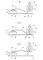
本発明のワイヤボンディング方法の第1の実施の形態を図1乃至図3により説明する。外部リード1が形成されたリードフレーム2上には、電極パッド3が形成されたダイ4がマウントされている。図3(b)に示すように、キャピラリ5にはワイヤ10が挿通されている。なお、6はクランパを示す。 A first embodiment of the wire bonding method of the present invention will be described with reference to FIGS. On the
まず、図1(a)に示す第1ボンド点Aにボンディングを行い、圧着ボール11と該圧着ボール11上にワイヤボンディング部12を形成する。この圧着ボール11及びワイヤボンディング部12の形成は、例えば特許文献3の方法で行う。即ち、図3(b)に示すように、クランパ6が閉じた状態でキャピラリ5の下端より延在するテール部13に図示しない電気トーチによる火花放電によってボール14を形成する。次にクランパ6は開いた状態となり、キャピラリ5が第1ボンド点Aの上方に移動した後に下降し、ボール14を第1ボンド点Aにボンディングして、図1(a)に示すように圧着ボール11を形成する。続いてキャピラリ5が上昇移動・水平移動等のループコントロールを行った後に圧着ボール11上にワイヤ10を圧着してワイヤボンディング部12を形成する。その後、キャピラリ5は外部リード1の第2ボンド点Bの僅かに上方に位置する。この場合、キャピラリ5の下端から余分のワイヤ10が垂れ下がった垂れ下がり部15が形成されている。 First, bonding is performed at a first bond point A shown in FIG. 1A to form a press-
次に図1(b)に示すように、キャピラリ5が下降してワイヤ10をリードフレーム2の外部リード1に押し付け、薄肉部16を形成する。このように、ワイヤ10を外部リード1に押し付けると、垂れ下がり部15が跳ね上がり、跳ね上がり部17となる。この場合、薄肉部16は外部リード1に完全に接続されなく、次の図1(c)工程でクランパ6が閉じてキャピラリ5が上昇する時、薄肉部16がキャピラリ5と共に持ち上げられる半接続状態に押し潰される。次にクランパ6が閉じて図1(c)に示すように、キャピラリ5は第1ボンド点Aの高さとほぼ同じ高さまで上昇する。 Next, as shown in FIG. 1B, the
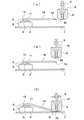
次に図2(a)に示すように、キャピラリ5は第1ボンド点Aから離れる方向に水平移動する。これにより、跳ね上がり部17が引っ張られてほぼ水平な直線状ワイヤ部18が形成されると共に、薄肉部16より切断される。続いて図2(b)に示すように、キャピラリ5は該キャピラリ5の下端が直線状ワイヤ部18の端部19の上方に位置するように移動する。次に図2(c)に示すように、キャピラリ5が下降し、直線状ワイヤ部18の端部19を外部リード1にボンディングする。この時、キャピラリ5の下端より僅かに伸びたワイヤ先端部20も外部リード1に接続される。 Next, as shown in FIG. 2A, the
次にクランパ6は開き、図3(a)(b)に示すように、キャピラリ5が上昇する。このキャピラリ5の上昇途中、即ち図3(a)に示すように上昇した時にクランパ6が閉じる。これにより、図3(b)に示すように、ワイヤ先端部20は外部リード1より剥がれ、キャピラリ5の下端にはテール部13が形成される。このテール部13に電気トーチによってボール14を形成した後に図1の工程に移る。 Next, the
このように、図1(c)から図2(a)の工程により跳ね上がり部17は引っ張られ、また薄肉部16より切断されて片持支持の直線状ワイヤ部18となる。この片持支持の直線状ワイヤ部18の端部19を図2(b)(c)に示すように、キャピラリ5によって押圧して第2ボンド点Bにボンディングするので、ワイヤループの直進性が向上する。 Thus, the bounce-up
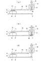
本発明のワイヤボンディング方法の第2の実施の形態を図4乃至図6により説明する。本実施の形態は、前記実施の形態と図1(a)から図2(a)までは同じである。図4(a)は図2(a)の状態を示す。前記実施の形態は、図2(a)の工程後、直線状ワイヤ部18の端部19をキャピラリ5により直接第2ボンド点Bにボンディングした。本実施の形態は、図4(a)(図2(a))の工程後、直線状ワイヤ部18の端部19をキャピラリ5により直接第2ボンド点Bにボンディングしない。 A second embodiment of the wire bonding method of the present invention will be described with reference to FIGS. The present embodiment is the same as the previous embodiment from FIG. 1A to FIG. 2A. FIG. 4A shows the state of FIG. In the embodiment, after the step of FIG. 2A, the
図4(a)の工程後、図4(b)に示すように、キャピラリ5が下降し、ワイヤ先端部20を外部リード1に軽く接続する。次にクランパ6は開き、図4(c)及び図5(a)に示すように、キャピラリ5が上昇する。このキャピラリ5の上昇途中、即ち図4(c)に示すように上昇した時にクランパ6が閉じる。これにより、図5(a)に示すように、ワイヤ先端部20は外部リード1より剥がれ、キャピラリ5の下端にはテール部25が形成される。このテール部25に図示しない電気トーチによる火花放電によってボール26を形成する。 After the step of FIG. 4A, the
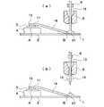
次にクランパ6は開いた状態となり、キャピラリ5は直線状ワイヤ部18の端部19の上方に移動する。続いて図5(c)に示すように、キャピラリ5が下降して直線状ワイヤ部18の端部19を外部リード1に押し付けると共に、ボール26を直線状ワイヤ部18の端部19上及び外部リード1にボンディングし、圧着ボール27を形成する。次に図6(a)(b)に示すように、キャピラリ5が上昇する。このキャピラリ5の上昇途中、即ち図6(a)に示すように上昇した時にクランパ6が閉じる。これにより、図6(b)に示すように、圧着ボール27の上端よりワイヤ10は切断され、キャピラリ5の下端にはテール部13が形成される。このテール部13に図示しない電気トーチによる火花放電によってボール14を形成した後に図1の工程に移る。 Next, the
本実施の形態においても片持支持の直線状ワイヤ部18の端部19を第2ボンド点Bにボンディングするので、前記実施の形態と同様にワイヤループの直進性が向上する。また本実施の形態においては、第2ボンド点Bにボンディングされた端部19に圧着ボール27を形成するので、第2ボンド点Bへのボンディングの肉厚が厚くなり、強度が向上する。 Also in this embodiment, since the
なお、上記実施の形態においては、第1ボンド点Aへのボンディングを特許文献3のボンディング方法でボンディングを行ったが、この方法に限定されるものではなく通常のボンディング方法でもよい。しかし、特許文献3のボンディング方法であると、第1ボンド点Aからの立ち上がりを低くすることができ好ましい。 In the above embodiment, the bonding to the first bond point A is performed by the bonding method of
A 第1ボンド点
B 第2ボンド点
1 外部リード
2 リードフレーム
3 電極パッド
4 ダイ
5 キャピラリ
6 クランパ
10 ワイヤ
11 圧着ボール
12 ワイヤボンディング部
15 垂れ下がり部
16 薄肉部
17 跳ね上がり部
18 直線状ワイヤ部
19 端部
20 ワイヤ先端部
25 テール部
26 ボール
27 圧着ボールA 1st bond point B
Claims (2)
Translated fromJapanesePriority Applications (4)
| Application Number | Priority Date | Filing Date | Title |
|---|---|---|---|
| JP2005328291AJP4530975B2 (en) | 2005-11-14 | 2005-11-14 | Wire bonding method |
| TW095133139ATW200735243A (en) | 2005-11-14 | 2006-09-08 | Method for wire bonding |
| KR1020060088860AKR100790372B1 (en) | 2005-11-14 | 2006-09-14 | Wire bonding method |
| US11/598,970US7621436B2 (en) | 2005-11-14 | 2006-11-14 | Wire bonding method |
Applications Claiming Priority (1)
| Application Number | Priority Date | Filing Date | Title |
|---|---|---|---|
| JP2005328291AJP4530975B2 (en) | 2005-11-14 | 2005-11-14 | Wire bonding method |
Publications (2)
| Publication Number | Publication Date |
|---|---|
| JP2007134611A JP2007134611A (en) | 2007-05-31 |
| JP4530975B2true JP4530975B2 (en) | 2010-08-25 |
Family
ID=38039725
Family Applications (1)
| Application Number | Title | Priority Date | Filing Date |
|---|---|---|---|
| JP2005328291AExpired - Fee RelatedJP4530975B2 (en) | 2005-11-14 | 2005-11-14 | Wire bonding method |
Country Status (4)
| Country | Link |
|---|---|
| US (1) | US7621436B2 (en) |
| JP (1) | JP4530975B2 (en) |
| KR (1) | KR100790372B1 (en) |
| TW (1) | TW200735243A (en) |
Families Citing this family (64)
| Publication number | Priority date | Publication date | Assignee | Title |
|---|---|---|---|---|
| US9833818B2 (en) | 2004-09-28 | 2017-12-05 | International Test Solutions, Inc. | Working surface cleaning system and method |
| KR101313391B1 (en) | 2004-11-03 | 2013-10-01 | 테세라, 인코포레이티드 | Stacked packaging improvements |
| US8058101B2 (en) | 2005-12-23 | 2011-11-15 | Tessera, Inc. | Microelectronic packages and methods therefor |
| JP4625858B2 (en)* | 2008-09-10 | 2011-02-02 | 株式会社カイジョー | Wire bonding method, wire bonding apparatus, and wire bonding control program |
| US9159708B2 (en) | 2010-07-19 | 2015-10-13 | Tessera, Inc. | Stackable molded microelectronic packages with area array unit connectors |
| US8482111B2 (en) | 2010-07-19 | 2013-07-09 | Tessera, Inc. | Stackable molded microelectronic packages |
| KR101075241B1 (en) | 2010-11-15 | 2011-11-01 | 테세라, 인코포레이티드 | Microelectronic package with terminals in dielectric member |
| US20120146206A1 (en) | 2010-12-13 | 2012-06-14 | Tessera Research Llc | Pin attachment |
| KR101128063B1 (en) | 2011-05-03 | 2012-04-23 | 테세라, 인코포레이티드 | Package-on-package assembly with wire bonds to encapsulation surface |
| US8618659B2 (en) | 2011-05-03 | 2013-12-31 | Tessera, Inc. | Package-on-package assembly with wire bonds to encapsulation surface |
| US8836136B2 (en) | 2011-10-17 | 2014-09-16 | Invensas Corporation | Package-on-package assembly with wire bond vias |
| US8946757B2 (en) | 2012-02-17 | 2015-02-03 | Invensas Corporation | Heat spreading substrate with embedded interconnects |
| US8372741B1 (en) | 2012-02-24 | 2013-02-12 | Invensas Corporation | Method for package-on-package assembly with wire bonds to encapsulation surface |
| US9349706B2 (en) | 2012-02-24 | 2016-05-24 | Invensas Corporation | Method for package-on-package assembly with wire bonds to encapsulation surface |
| US8835228B2 (en) | 2012-05-22 | 2014-09-16 | Invensas Corporation | Substrate-less stackable package with wire-bond interconnect |
| US9502371B2 (en) | 2012-07-17 | 2016-11-22 | Kulicke And Soffa Industries, Inc. | Methods of forming wire interconnect structures |
| US9391008B2 (en) | 2012-07-31 | 2016-07-12 | Invensas Corporation | Reconstituted wafer-level package DRAM |
| US9502390B2 (en) | 2012-08-03 | 2016-11-22 | Invensas Corporation | BVA interposer |
| US8975738B2 (en) | 2012-11-12 | 2015-03-10 | Invensas Corporation | Structure for microelectronic packaging with terminals on dielectric mass |
| US8878353B2 (en) | 2012-12-20 | 2014-11-04 | Invensas Corporation | Structure for microelectronic packaging with bond elements to encapsulation surface |
| US9136254B2 (en) | 2013-02-01 | 2015-09-15 | Invensas Corporation | Microelectronic package having wire bond vias and stiffening layer |
| JP2014207430A (en) | 2013-03-21 | 2014-10-30 | ローム株式会社 | Semiconductor device |
| US9034696B2 (en) | 2013-07-15 | 2015-05-19 | Invensas Corporation | Microelectronic assemblies having reinforcing collars on connectors extending through encapsulation |
| US8883563B1 (en) | 2013-07-15 | 2014-11-11 | Invensas Corporation | Fabrication of microelectronic assemblies having stack terminals coupled by connectors extending through encapsulation |
| US9023691B2 (en) | 2013-07-15 | 2015-05-05 | Invensas Corporation | Microelectronic assemblies with stack terminals coupled by connectors extending through encapsulation |
| US9093515B2 (en)* | 2013-07-17 | 2015-07-28 | Freescale Semiconductor, Inc. | Wire bonding capillary with working tip protrusion |
| US9167710B2 (en) | 2013-08-07 | 2015-10-20 | Invensas Corporation | Embedded packaging with preformed vias |
| US9685365B2 (en) | 2013-08-08 | 2017-06-20 | Invensas Corporation | Method of forming a wire bond having a free end |
| US20150076714A1 (en) | 2013-09-16 | 2015-03-19 | Invensas Corporation | Microelectronic element with bond elements to encapsulation surface |
| US9082753B2 (en) | 2013-11-12 | 2015-07-14 | Invensas Corporation | Severing bond wire by kinking and twisting |
| US9087815B2 (en) | 2013-11-12 | 2015-07-21 | Invensas Corporation | Off substrate kinking of bond wire |
| US9379074B2 (en) | 2013-11-22 | 2016-06-28 | Invensas Corporation | Die stacks with one or more bond via arrays of wire bond wires and with one or more arrays of bump interconnects |
| US9583456B2 (en) | 2013-11-22 | 2017-02-28 | Invensas Corporation | Multiple bond via arrays of different wire heights on a same substrate |
| US9263394B2 (en) | 2013-11-22 | 2016-02-16 | Invensas Corporation | Multiple bond via arrays of different wire heights on a same substrate |
| US9583411B2 (en) | 2014-01-17 | 2017-02-28 | Invensas Corporation | Fine pitch BVA using reconstituted wafer with area array accessible for testing |
| TWI543284B (en)* | 2014-02-10 | 2016-07-21 | 新川股份有限公司 | Method for producing semiconductor apparatus and wire bonding apparatus |
| JP5686912B1 (en)* | 2014-02-20 | 2015-03-18 | 株式会社新川 | Bump forming method, bump forming apparatus, and semiconductor device manufacturing method |
| US9214454B2 (en) | 2014-03-31 | 2015-12-15 | Invensas Corporation | Batch process fabrication of package-on-package microelectronic assemblies |
| US10381326B2 (en) | 2014-05-28 | 2019-08-13 | Invensas Corporation | Structure and method for integrated circuits packaging with increased density |
| US9646917B2 (en) | 2014-05-29 | 2017-05-09 | Invensas Corporation | Low CTE component with wire bond interconnects |
| US9412714B2 (en) | 2014-05-30 | 2016-08-09 | Invensas Corporation | Wire bond support structure and microelectronic package including wire bonds therefrom |
| TWI567839B (en)* | 2014-08-27 | 2017-01-21 | 矽品精密工業股份有限公司 | Wire bond structure and wire bonding fabrication method |
| US9735084B2 (en) | 2014-12-11 | 2017-08-15 | Invensas Corporation | Bond via array for thermal conductivity |
| US9888579B2 (en) | 2015-03-05 | 2018-02-06 | Invensas Corporation | Pressing of wire bond wire tips to provide bent-over tips |
| US9530749B2 (en) | 2015-04-28 | 2016-12-27 | Invensas Corporation | Coupling of side surface contacts to a circuit platform |
| US9502372B1 (en) | 2015-04-30 | 2016-11-22 | Invensas Corporation | Wafer-level packaging using wire bond wires in place of a redistribution layer |
| US9761554B2 (en) | 2015-05-07 | 2017-09-12 | Invensas Corporation | Ball bonding metal wire bond wires to metal pads |
| US9490222B1 (en) | 2015-10-12 | 2016-11-08 | Invensas Corporation | Wire bond wires for interference shielding |
| US10490528B2 (en) | 2015-10-12 | 2019-11-26 | Invensas Corporation | Embedded wire bond wires |
| US10332854B2 (en) | 2015-10-23 | 2019-06-25 | Invensas Corporation | Anchoring structure of fine pitch bva |
| US10181457B2 (en) | 2015-10-26 | 2019-01-15 | Invensas Corporation | Microelectronic package for wafer-level chip scale packaging with fan-out |
| US10043779B2 (en) | 2015-11-17 | 2018-08-07 | Invensas Corporation | Packaged microelectronic device for a package-on-package device |
| US9659848B1 (en) | 2015-11-18 | 2017-05-23 | Invensas Corporation | Stiffened wires for offset BVA |
| US9984992B2 (en) | 2015-12-30 | 2018-05-29 | Invensas Corporation | Embedded wire bond wires for vertical integration with separate surface mount and wire bond mounting surfaces |
| US9935075B2 (en) | 2016-07-29 | 2018-04-03 | Invensas Corporation | Wire bonding method and apparatus for electromagnetic interference shielding |
| US10299368B2 (en) | 2016-12-21 | 2019-05-21 | Invensas Corporation | Surface integrated waveguides and circuit structures therefor |
| US9825000B1 (en) | 2017-04-24 | 2017-11-21 | International Test Solutions, Inc. | Semiconductor wire bonding machine cleaning device and method |
| WO2019165305A1 (en) | 2018-02-23 | 2019-08-29 | International Test Solutions, Inc. | Novel material and hardware to automatically clean flexible electronic web rolls |
| US11756811B2 (en) | 2019-07-02 | 2023-09-12 | International Test Solutions, Llc | Pick and place machine cleaning system and method |
| US10792713B1 (en) | 2019-07-02 | 2020-10-06 | International Test Solutions, Inc. | Pick and place machine cleaning system and method |
| US11211242B2 (en) | 2019-11-14 | 2021-12-28 | International Test Solutions, Llc | System and method for cleaning contact elements and support hardware using functionalized surface microfeatures |
| US11318550B2 (en) | 2019-11-14 | 2022-05-03 | International Test Solutions, Llc | System and method for cleaning wire bonding machines using functionalized surface microfeatures |
| US11035898B1 (en) | 2020-05-11 | 2021-06-15 | International Test Solutions, Inc. | Device and method for thermal stabilization of probe elements using a heat conducting wafer |
| US12057431B2 (en)* | 2020-12-18 | 2024-08-06 | Kulicke And Soffa Industries, Inc. | Methods of forming wire interconnect structures and related wire bonding tools |
Family Cites Families (9)
| Publication number | Priority date | Publication date | Assignee | Title |
|---|---|---|---|---|
| JPS5925377B2 (en)* | 1980-04-05 | 1984-06-16 | 株式会社新川 | Wire bonding method |
| JP2789395B2 (en) | 1991-06-19 | 1998-08-20 | 株式会社新川 | Wire bonding method |
| JPH0951011A (en) | 1995-08-10 | 1997-02-18 | Tanaka Denshi Kogyo Kk | Wire bonding method for semiconductor chips |
| DE19823623A1 (en)* | 1998-05-27 | 1999-12-02 | Bosch Gmbh Robert | Method and contact point for establishing an electrical connection |
| JP3422937B2 (en)* | 1998-07-27 | 2003-07-07 | 株式会社新川 | Ball forming method in wire bonding |
| JP2000082717A (en) | 1998-09-07 | 2000-03-21 | Shinkawa Ltd | Wire bonding method |
| JP2000200802A (en)* | 1998-12-31 | 2000-07-18 | Texas Instr Inc <Ti> | System for very long bonding wire in semiconductor device and method |
| JP3455126B2 (en)* | 1999-03-02 | 2003-10-14 | 株式会社新川 | Wire bonding method |
| JP2005167178A (en)* | 2003-11-10 | 2005-06-23 | Shinkawa Ltd | Semiconductor device and wire bonding method |
- 2005
- 2005-11-14JPJP2005328291Apatent/JP4530975B2/ennot_activeExpired - Fee Related
- 2006
- 2006-09-08TWTW095133139Apatent/TW200735243A/enunknown
- 2006-09-14KRKR1020060088860Apatent/KR100790372B1/ennot_activeExpired - Fee Related
- 2006-11-14USUS11/598,970patent/US7621436B2/ennot_activeExpired - Fee Related
Also Published As
| Publication number | Publication date |
|---|---|
| US7621436B2 (en) | 2009-11-24 |
| JP2007134611A (en) | 2007-05-31 |
| US20070108256A1 (en) | 2007-05-17 |
| KR20070051658A (en) | 2007-05-18 |
| KR100790372B1 (en) | 2008-01-02 |
| TW200735243A (en) | 2007-09-16 |
Similar Documents
| Publication | Publication Date | Title |
|---|---|---|
| JP4530975B2 (en) | Wire bonding method | |
| JP4298665B2 (en) | Wire bonding method | |
| JP3854232B2 (en) | Bump forming method and wire bonding method | |
| JP4509043B2 (en) | Stud bump formation method | |
| JP4106039B2 (en) | Wire bonding method | |
| US20070029367A1 (en) | Semiconductor device | |
| JP4021378B2 (en) | Wire bonding method | |
| JP4088015B2 (en) | Method for forming curved wire | |
| US6352197B1 (en) | Method and apparatus for wire-bonding for electric components | |
| JP4105996B2 (en) | Wire bonding method | |
| JP2005167178A (en) | Semiconductor device and wire bonding method | |
| JP2015106548A (en) | Crimping method of electric wire to terminal | |
| KR100718889B1 (en) | Wire Bonding Capillary with Two-Step High Bottleneck | |
| JP4369401B2 (en) | Wire bonding method | |
| JP2012099556A (en) | Method for manufacturing semiconductor device | |
| JP4547405B2 (en) | Wire bonding method | |
| JP4879923B2 (en) | Semiconductor device | |
| JP4215693B2 (en) | Wire bonding method | |
| JP2002280412A (en) | Wire-bonding method | |
| JPH05235002A (en) | Bump forming method | |
| JP2017059775A (en) | Semiconductor device, lead frame and manufacturing method of the same | |
| JP2012064733A (en) | Method of manufacturing semiconductor device and semiconductor manufacturing apparatus | |
| JP2006173304A (en) | Lead frame manufacturing method and lead frame | |
| JP2007042764A (en) | Bump forming method, shape of bump or semiconductor device | |
| JPH113905A (en) | Semiconductor device, method of manufacturing the same, and lead frame used in the manufacture thereof |
Legal Events
| Date | Code | Title | Description |
|---|---|---|---|
| A621 | Written request for application examination | Free format text:JAPANESE INTERMEDIATE CODE: A621 Effective date:20071214 | |
| A977 | Report on retrieval | Free format text:JAPANESE INTERMEDIATE CODE: A971007 Effective date:20100108 | |
| A131 | Notification of reasons for refusal | Free format text:JAPANESE INTERMEDIATE CODE: A131 Effective date:20100119 | |
| A521 | Request for written amendment filed | Free format text:JAPANESE INTERMEDIATE CODE: A523 Effective date:20100203 | |
| A131 | Notification of reasons for refusal | Free format text:JAPANESE INTERMEDIATE CODE: A131 Effective date:20100405 | |
| A521 | Request for written amendment filed | Free format text:JAPANESE INTERMEDIATE CODE: A523 Effective date:20100423 | |
| TRDD | Decision of grant or rejection written | ||
| A01 | Written decision to grant a patent or to grant a registration (utility model) | Free format text:JAPANESE INTERMEDIATE CODE: A01 Effective date:20100517 | |
| A01 | Written decision to grant a patent or to grant a registration (utility model) | Free format text:JAPANESE INTERMEDIATE CODE: A01 | |
| A61 | First payment of annual fees (during grant procedure) | Free format text:JAPANESE INTERMEDIATE CODE: A61 Effective date:20100608 | |
| R150 | Certificate of patent or registration of utility model | Free format text:JAPANESE INTERMEDIATE CODE: R150 | |
| FPAY | Renewal fee payment (event date is renewal date of database) | Free format text:PAYMENT UNTIL: 20130618 Year of fee payment:3 | |
| LAPS | Cancellation because of no payment of annual fees |