JP4527456B2 - Memory life warning device and information processing method - Google Patents
Memory life warning device and information processing methodDownload PDFInfo
- Publication number
- JP4527456B2 JP4527456B2JP2004199222AJP2004199222AJP4527456B2JP 4527456 B2JP4527456 B2JP 4527456B2JP 2004199222 AJP2004199222 AJP 2004199222AJP 2004199222 AJP2004199222 AJP 2004199222AJP 4527456 B2JP4527456 B2JP 4527456B2
- Authority
- JP
- Japan
- Prior art keywords
- write
- sectors
- semiconductor memory
- memory
- life
- Prior art date
- Legal status (The legal status is an assumption and is not a legal conclusion. Google has not performed a legal analysis and makes no representation as to the accuracy of the status listed.)
- Expired - Fee Related
Links
Images


Landscapes
- Techniques For Improving Reliability Of Storages (AREA)
- Debugging And Monitoring (AREA)
Description
Translated fromJapanese本発明は、半導体メモリを含むメモリカードなどの小型メモリモジュールが記憶装置として情報処理装置で使用される際、半導体メモリの書き込み寿命を操作者に対して通知するメモリ寿命警告装置、およびその通知のための情報処理方法に関する。 The present invention relates to a memory life warning device for notifying an operator of a write life of a semiconductor memory when a small memory module such as a memory card including a semiconductor memory is used as a storage device in an information processing device, and a notification of the notification The present invention relates to an information processing method.
メモリカードなどの小型メモリモジュールに用いられる半導体メモリに不揮発性メモリがある。不揮発性メモリの一種であるフラッシュメモリは、データ消去・書き込みのサイクルに特性上限度がある。現状、NAND型フラッシュメモリで1つの記憶素子に対して書き込み可能な回数は数十万回程度である。記憶領域がフラッシュメモリの記憶素子で構成される小型メモリモジュールも当然、書き込み回数の限界(寿命)がある。そのため、この寿命は、情報処理装置の設計段階で、メモリモジュールへのデータの書き込み回数や書き込み情報量を試算した後、設定される。そして、このように設定された寿命を前提として、情報処理装置の稼動時間でメモリモジュールの耐用時間(年数)を割り出していた。 Non-volatile memories are semiconductor memories used for small memory modules such as memory cards. A flash memory, which is a kind of nonvolatile memory, has a characteristic upper limit in a data erasing / writing cycle. At present, the number of times that data can be written to one storage element in the NAND flash memory is about several hundred thousand times. Naturally, a small memory module whose storage area is composed of a storage element of a flash memory also has a limit on the number of times of writing (life). Therefore, this lifetime is set after trial calculation of the number of times data is written to the memory module and the amount of information to be written at the design stage of the information processing apparatus. And assuming the lifetime set in this way, the useful life (years) of the memory module is determined by the operating time of the information processing apparatus.
また、書き込み回数の寿命をより正確に把握するために、記憶素子毎に書き込み回数を管理するものもある(例えば、特許文献1参照)。
従来の寿命判定方法では、書き込み回数および書き込み情報量が変動する場合や、情報処理装置の休止時間と稼動時間の配分が変化する場合には当てはまらず、全てのメモリモジュールの寿命について情報処理装置の稼働時間で推し量ることは困難である。 The conventional life determination method does not apply to the case where the number of writes and the amount of written information fluctuate or the distribution of the downtime and the operating time of the information processing device changes. It is difficult to estimate by operating time.
メモリモジュールの書き込み寿命の残りを知るためには、全記憶素子に対して書き込み回数をカウントするのが最良である。しかし、全記憶素子に対してカウント数を管理するには、メモリモジュール内のフラッシュメモリの記憶素子全てについてカウント数を記録する必要があり、そのデータを保持するためのメモリが膨大になり現実的でない。記録単位として記憶素子の代わりにセクタで管理しても同様である。 In order to know the remaining write life of the memory module, it is best to count the number of writes to all memory elements. However, in order to manage the count number for all the memory elements, it is necessary to record the count number for all the memory elements of the flash memory in the memory module. Not. The same is true if the recording unit is managed by sectors instead of storage elements.
本発明は、上述したような従来の技術が有する問題点を解決するためになされたものであり、使用される半導体メモリに即した書き込み寿命をより簡便な方法でより正確に通知可能にしたメモリ寿命警告装置、およびその通知のための情報処理方法を提供することを目的とする。 The present invention has been made in order to solve the above-described problems of the prior art, and a memory capable of more accurately notifying a write life corresponding to a semiconductor memory to be used by a simpler method. An object of the present invention is to provide a life warning device and an information processing method for the notification.
上記目的を達成するための本発明のメモリ寿命警告装置は、情報処理装置に用いられる半導体メモリについての書き込み寿命を通知するためのメモリ寿命警告装置であって、
前記半導体メモリを装着するためのアダプタ部と、
書き込み寿命である旨を表示するための表示部と、
前記半導体メモリの使用状況に対応して該半導体メモリの書き込み命令限界回数を算定するとともに、該情報処理装置から該半導体メモリへの書き込み命令の回数をカウントする命令計数回路と、
前記書き込み命令限界回数を保持するための記憶部と、
前記書き込み命令の回数と前記書き込み命令限界回数とを比較し、該書き込み命令の回数が該書き込み命令限界回数を越えると、前記表示部に書き込み寿命である旨を表示させる比較部と、を有し、
前記命令計数回路は、
前記書き込み命令の回数と該書き込み命令毎の書き込みセクタ数とを所定の期間計測した後、該書き込みセクタ数の和を該書き込み命令の回数で割ることで一回あたりの書き込み時におけるセクタ数である平均セクタ数を算出し、該半導体メモリの全セクタの書き込み可能回数を該平均セクタ数で割った値を前記書き込み命令限界回数とする構成である。The memory life warning device of the present invention for achieving the above object is a memory life warning device for notifying the write life of a semiconductor memory used in an information processing device,
An adapter for mounting the semiconductor memory;
A display for displaying that the writing life is reached;
An instruction counting circuit for calculating the write command limit number of the semiconductor memory corresponding to the use state of the semiconductor memory, and counting the number of write commands from the information processing device to the semiconductor memory;
A storage unit for holding the write command limit number of times;
Comparing the write command limit number and the number of the write command, the number of the write command exceeds the write command limit number, havea, a comparing unit for displaying the effect that the writing lifetime on the display unit,
The instruction counting circuit includes:
After measuring the number of write commands and the number of write sectors for each write command for a predetermined period, the total number of write sectors is divided by the number of write commands to obtain the number of sectors per write. An average number of sectors is calculated, and a value obtained by dividing the number of writable times in all sectors of the semiconductor memory by the average number of sectors is set as the write command limit number .
本発明では、半導体メモリの使用状況に対応して半導体メモリの書き込み命令限界回数が算定される。そのため、半導体メモリ毎に寿命が近づいた段階で、表示部により書き込み寿命の警告が表示され、操作者に半導体メモリが寿命である旨が通知される。 In the present invention, the write command limit number of the semiconductor memory is calculated in accordance with the use state of the semiconductor memory. For this reason, when the lifetime of each semiconductor memory approaches, a warning about the write lifetime is displayed on the display unit, and the operator is notified that the semiconductor memory is at the end of its lifetime.
本発明では、書き込み命令の回数と書き込み命令毎の書き込みセクタ数とが所定の期間計測され、その計測結果により書き込み命令限界回数が算定される。そのため、半導体メモリへの書き込み命令の回数および書き込み情報量が変動する場合でも一定の期間計測され、その変動が書き込み命令限界回数に反映される。また、情報処理装置の休止時間と稼動時間の配分が一定の期間計測され、その時間配分の変化が書き込み命令限界回数に反映される。 In the present invention, the number of write commands and the number of write sectors for each write command are measured for a predetermined period, and the write command limit number is calculated from the measurement result. Therefore, even when the number of write commands to the semiconductor memory and the amount of write information fluctuate, the measurement is performed for a certain period, and the fluctuation is reflected in the write command limit number. In addition, the distribution of the downtime and the operation time of the information processing apparatus is measured for a certain period, and the change in the time distribution is reflected in the write command limit number.
一方、上記目的を達成するための本発明の情報処理方法は、情報処理装置に用いられる半導体メモリについての書き込み寿命を通知するための、記憶部および表示部を備えたメモリ寿命警告装置による情報処理方法であって、
前記半導体メモリの使用状況に対応して該半導体メモリの書き込み命令限界回数を算定し、
前記書き込み命令限界回数を前記記憶部に保持し、
前記情報処理装置から半導体メモリへの書き込み命令の回数をカウントし、
前記書き込み命令の回数と前記書き込み命令限界回数とを比較し、
前記書き込み命令の回数が前記書き込み命令限界回数を越えると、前記表示部に該書き込み寿命である旨を表示させるものであり、
前記書き込み命令限界回数の算定方法は、
前記書き込み命令の回数と該書き込み命令毎の書き込みセクタ数とを所定の期間計測した後、
前記所定の期間における前記書き込みセクタ数の和を前記書き込み命令の回数で割ることで、一回あたりの書き込み時におけるセクタ数である平均セクタ数を算出し、
その後、前記半導体メモリの全セクタの書き込み可能回数を前記平均セクタ数で割った値を前記書き込み命令限界回数とするものである。On the other hand, the information processing method of the present invention for achieving the above object is an information processing by a memory life warning device having a storage unit and a display unit for notifying a write life of a semiconductor memory used in the information processing device. A method,
Calculate the write command limit number of the semiconductor memory corresponding to the use status of the semiconductor memory,
Holding the write command limit number in the storage unit;
Count the number of write commands from the information processing device to the semiconductor memory,
Compare the number of write commands with the limit number of write commands,
When the number of write commands exceeds the limit number of write commands, the display unit displays that it is the write life,
The calculation method of the write command limit number of times,
After measuring the number of write commands and the number of write sectors for each write command for a predetermined period,
By dividing the sum of the number of write sectors in the predetermined period by the number of write commands, the average number of sectors that are the number of sectors at the time of writing is calculated,
Thereafter, a value obtained by dividing the number of writable times in all sectors of the semiconductor memory by the average number of sectors is set as the write command limit number .
本発明のメモリ寿命警告装置は、寿命を有する記憶装置に対して書き込み回数や書き込みデータ量を考慮したうえで、寿命回数を設定し、リアルタイムで残り寿命を監視するため、記憶装置部品の交換を操作者に明示的に知らせることが可能となる。これにより、記憶装置がフラッシュメモリであれば、情報処理装置がフラッシュメモリを用いたメモリカードを含めたシステムとしてまだ安定に稼動するのか、メモリカードを新品と交換する時期に到達しているのか操作者が容易に判断できるようになる。 The memory life warning device of the present invention sets the number of times of life after monitoring the number of times of writing and the amount of data to be written to the storage device having the life and monitors the remaining life in real time. It is possible to explicitly notify the operator. Thus, if the storage device is a flash memory, whether the information processing device is still operating stably as a system including a memory card using the flash memory or whether it is time to replace the memory card with a new one Can easily judge.
また、操作者はフラッシュメモリを用いたメモリモジュールの寿命を知ることが可能となるため、メモリモジュール部品をコスト的に最適時期に交換できる。 In addition, since the operator can know the life of the memory module using the flash memory, the memory module components can be replaced at an optimal time in terms of cost.
さらに、メモリモジュール部品が故障した際、故障原因が「書き込み寿命」によるものか他の原因なのか、操作者は即座に判断できる。 Furthermore, when a memory module component fails, the operator can immediately determine whether the cause of the failure is due to the “write life” or another cause.
本発明によるメモリ寿命警告装置は、半導体メモリの使用状況から書き込み寿命を予測する回路と、書き込み命令の回数が予測した書き込み寿命に達したか否かを判定する比較部と、書き込み寿命に達した際に警告表示する表示部とを有することを特徴とする。 A memory life warning device according to the present invention includes a circuit for predicting a write life from the use state of a semiconductor memory, a comparison unit for determining whether the number of write instructions has reached the predicted write life, and a write life has been reached. And a display unit for displaying a warning at the time.
本発明の構成について説明する。 The configuration of the present invention will be described.
図1はメモリ寿命警告装置の一構成例を示す図である。 FIG. 1 is a diagram showing a configuration example of a memory life warning device.
図1に示すように、メモリ寿命警告装置は、フラッシュメモリカードアダプタ部11と、書き込み命令回数計数回路12と、書き込み命令限界回数記憶部13と、書き込み命令回数および書き込み命令限界回数の大きさを比較する比較部14と、寿命判定表示部15とを有する構成である。なお、以下では、フラッシュメモリカードアダプタ部をアダプタ部と称し、書き込み命令回数計数回路を命令計数回路と称し、書き込み命令限界回数記憶部を限界回数記憶部と称する。また、書き込み命令の回数をnとおき、書き込み命令限界回数をNとおいて、比較部を(N,n)比較部と表記する。 As shown in FIG. 1, the memory life warning device compares the size of the flash memory
メモリ寿命警告装置は、コンピュータ30の接続バスに取り付けられ、コンピュータ30から電源と時刻の情報が供給される。コンピュータ30は、パーソナルコンピュータ、ワークステーションおよび携帯情報端末等の情報処理装置である。小型メモリモジュールとなるフラッシュメモリカード(以下、単にメモリカードと称する)20はアダプタ部11に装着される。メモリカード20に記憶されているデータについてのコンピュータ30からのデータ読み込み要求や、コンピュータ30側データのメモリカード20へのデータ書き込み要求などの信号は、コンピュータ30からアダプタ部11を経由してメモリカード20に到達し、要求に基づく処理が実行される。メモリカード20には、メモリカード毎に異なる識別子であるID(Identification)が登録されている。 The memory life warning device is attached to the connection bus of the
命令計数回路12は、メモリ寿命警告装置がコンピュータ30の接続バスに装着されると、コンピュータ30から受け取る時刻の情報を参照して所定の期間メモリカード20への書き込み命令の回数と書き込み命令毎のセクタ数を計測し、一回あたりの書き込み時におけるセクタ数である平均セクタ数を算出した後、メモリカード20の全セクタの書き込み可能回数を平均セクタ数で除した結果の値を書き込み命令限界回数として算定する。書き込み命令限界回数を算定した後、アダプタ部11を介してコンピュータ30から書き込み命令のパルスを受ける度にカウントする。 When the memory life warning device is mounted on the connection bus of the
限界回数記憶部13は、不揮発性メモリなどで構成される記憶回路であり、命令計数回路12が算定した書き込み命令限界回数を保持する。また、メモリカード20がアダプタ部11から取り外される際、メモリカード20のIDと、そのメモリカード20についての書き込み命令の回数とが登録される。命令計数回路12は、メモリカード20がアダプタ部11に装着されると、メモリカード20に登録されたIDを読み出して、読み出したIDが限界回路記憶部13に登録されているか否かを調べる。そのIDが既に登録されていれば、IDと一緒に登録された書き込み命令の回数を読み出して、その回数を継続してカウントする。読み出したIDが限界回路記憶部13に登録されていなければ、書き込み命令の回数をはじめからカウントする。 The limit
このようにして、メモリカードが入れ替えられる毎にメモリカード毎に書き込み命令の回数が継続してカウントされる。そのため、メモリカード毎に書き込み寿命まで使用可能となる。 In this way, every time a memory card is replaced, the number of write commands is continuously counted for each memory card. Therefore, the memory card can be used until the writing life.
(N,n)比較部14は、メモリカード毎に書き込み命令限界回数と書き込み命令の回数とを比較し、書き込み命令の回数が書き込み命令限界回数を越えると、警告ランプを点灯する旨を示す点灯信号を寿命判定表示部15に送信する。 The (N, n)
寿命判定表示部15は、メモリカードへの書き込み命令の回数が限界値になったことを操作者に通知するための警告ランプを備え、(N,n)比較部14から点灯信号を受信すると、警告ランプを点灯する。 The life
次に、上述の構成のメモリ寿命警告装置の動作について説明する。 Next, the operation of the memory life warning device having the above-described configuration will be described.
図2はメモリ寿命警告装置の動作手順を示すフローチャートである。 FIG. 2 is a flowchart showing the operation procedure of the memory life warning device.
操作者がメモリ寿命警告装置をコンピュータ30に接続し、メモリカード20をアダプタ部11に装着してコンピュータ30の電源をオンすると、命令計数回路12が、後述する方法で書き込み命令限界回数を算定する(ステップS1)。ここでは、書き込み命令限界回数を10万回と算定したものとする。そして、命令計数回路12は、算定した書き込み命令限界回数を限界回数記憶部13に入力すると(ステップS2)、限界回数記憶部13は書き込み命令限界回数を保持する。 When the operator connects the memory life warning device to the
その後、命令計数回路12は、メモリカード20への書き込み命令がある毎にカウントする(ステップS3)。(N,n)比較部14は、命令計数回路12がカウントする度に、書き込み命令の回数nと書き込み命令限界回数Nの大きさを比較する(ステップS4)。nの値がNの値より小さいか等しい場合、ステップS3に戻り、命令計数回路12は書き込み命令の回数のカウントを続ける。一方、nの値がNの値よりも大きい場合、例えば、nが100001のとき、(N,n)比較部14は点灯信号を寿命判定表示部15に送信する。寿命判定表示部15は、点灯信号を受信すると、警告ランプを点灯する(ステップS5)。 Thereafter, the instruction counting circuit 12 counts every time there is a write instruction to the memory card 20 (step S3). Each time the instruction counting circuit 12 counts, the (N, n)
次に、命令計数回路12が実施する、書き込み命令限界回数の算定方法について説明する。 Next, a method of calculating the write command limit number performed by the command counting circuit 12 will be described.
図3は、書き込み命令限界回数の算定の仕方を説明するための図である。 FIG. 3 is a diagram for explaining how to calculate the write command limit number.
図3に示すように、コンピュータ30が記憶装置としてメモリカード20を使用することで、コンピュータ30とメモリカード20が1つのシステムとして機能する。メモリカード20の使用状況はシステム毎で異なってくる。一回の書き込みで、セクタの数が大きかったり、少なかったりする。本発明では、メモリカード20の使用状況に対応して書き込み命令限界回数を算定する際、メモリカード20の使用状況を、以下のように調べる。メモリカード20に対して、どのような書き込み命令があるのかを一定時間、例えば、1日(24時間)計測する。 As shown in FIG. 3, when the
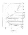
図4はメモリカードの使用状況の調査結果を示すグラフである。グラフの縦軸は出現度数を示し、グラフの横軸は一回の書き込みセクタ数であるライトセクタ数を示す。 FIG. 4 is a graph showing the results of investigation of the usage status of the memory card. The vertical axis of the graph indicates the frequency of appearance, and the horizontal axis of the graph indicates the number of write sectors, which is the number of write sectors at one time.
図4に示す実線グラフと破線グラフは、それぞれ異なるシステムによるメモリカード使用状況を示す。全体としてみると、実線グラフの場合よりも破線グラフの場合の方が、一回の書き込みのセクタ数が大きいことがわかる。同一の業務であれば、グラフの形状は類似の曲線パターンを描くという特性から、これは、システムが利用される業務が異なるためと考えられる。このように、業務によりメモリカードの使用状況が異なるため、その使用状況に合わせて命令限界回数を算定する必要がある。以下に、図4に示した実線グラフの場合で、命令限界回数の算定方法について説明する。 The solid line graph and the broken line graph shown in FIG. As a whole, it can be seen that the number of sectors for one writing is larger in the case of the broken line graph than in the case of the solid line graph. If the business is the same, the shape of the graph draws a similar curve pattern, which is considered to be because the business in which the system is used is different. As described above, since the usage status of the memory card varies depending on the business, it is necessary to calculate the instruction limit number according to the usage status. Hereinafter, a method for calculating the instruction limit number in the case of the solid line graph shown in FIG. 4 will be described.
図4の実線グラフに示すように、一回の書き込み命令で書き込むデータ量が様々に変化している。ライトセクタ数は8、16、32と離散的に変化する。ライトセクタ数128はライトセクタ数8の16倍のデータを一度に書き込むことを意味する。はじめに、1日で何回書き込み命令を実行したかを計算する。 As shown in the solid line graph of FIG. 4, the amount of data written by a single write command changes variously. The number of write sectors varies discretely as 8, 16, 32. The number of
図4より、3 + 220 + 660 + 770 + 82 + 23 + 9 + 7 + 5 = 1777 (回)となる。続いて、書き込み総セクタ数を求めると、
3×8+220×16+660×32+770×48+82×64+23×80+9×96+7×112+5×128 = 71000 (セクタ)となる。From FIG. 4, 3 + 220 + 660 + 770 + 82 + 23 + 9 + 7 + 5 = 1777 (times). Next, when calculating the total number of sectors written,
3 × 8 + 220 × 16 + 660 × 32 + 770 × 48 + 82 × 64 + 23 × 80 + 9 × 96 + 7 × 112 + 5 × 128 = 71000 (sectors).
求めた2つの値から一回あたりの書き込みセクタ数である平均セクタ数を求めると、
71000÷1777 = 39.95 セクタ/回≒ 40 セクタ/回となる。When the average number of sectors, which is the number of write sectors per time, is obtained from the obtained two values,
71000 ÷ 1777 = 39.95 sectors / time ≒ 40 sectors / time.
一方、フラッシュメモリカードの書き込み容量が1000セクタあり、1セクタあたり10万回の書き込み寿命があるとすれば、
1000セクタ×10万回=1億セクタ・回となる。このことから、1億セクタ・回の延べ書き込み回数があることになる。On the other hand, if the flash memory card has a write capacity of 1000 sectors and a write life of 100,000 times per sector,
1000 sectors x 100,000 times = 100 million sectors. Thus, there are a total of 100 million sectors / times.
これを1回の書き込み命令に対して換算すると、
1億÷40=250万回書き込み命令となり、書き込み命令限界回数Nを250万回と算定することができる。この値Nを図1の限界回数記憶部13に入力する。When this is converted to one write command,
100 million ÷ 40 = 2.5 million write commands, and the write command limit number N can be calculated as 2.5 million. This value N is input to the limit
上述のことから、メモリカード20の書き込み容量をV、1セクタあたりの書き込み寿命をT、所定期間の書き込み総セクタ数をM、所定期間の書き込み命令数をSとすると、書き込み命令限界回数Nを求める式は、
N=(V×T)/(M/S)となる。From the above, when the write capacity of the
N = (V × T) / (M / S).
本発明では、上述したように、システム毎に書き込み命令の回数および書き込み情報量を一定の期間計測した後、計測結果から半導体メモリの書き込み命令限界回数を算定している。そのため、半導体メモリへの書き込み命令の回数および書き込み情報量が変動する場合でも一定の期間計測され、その変動が書き込み命令限界回数に反映される。また、情報処理装置の休止時間と稼動時間の配分が一定の期間計測され、その時間配分の変化が書き込み命令限界回数に反映される。このようにして、半導体メモリの使用状況に対応した書き込み命令限界回数が算定されることで、半導体メモリ毎に寿命が近づいた段階で、書き込み寿命の警告が表示部により表示され、操作者に半導体メモリが寿命である旨が通知される。 In the present invention, as described above, the number of write commands and the amount of write information are measured for each system for a certain period, and then the write command limit number of the semiconductor memory is calculated from the measurement result. Therefore, even when the number of write commands to the semiconductor memory and the amount of write information fluctuate, the measurement is performed for a certain period, and the fluctuation is reflected in the write command limit number. In addition, the distribution of the downtime and the operation time of the information processing apparatus is measured for a certain period, and the change in the time distribution is reflected in the write command limit number. In this way, the write command limit number corresponding to the use state of the semiconductor memory is calculated, and when the life of each semiconductor memory approaches, the write life warning is displayed on the display unit, and the semiconductor is displayed to the operator. You are notified that the memory is out of life.
また、半導体メモリの記憶素子毎に書き込み命令の回数をカウントする必要がないため、全ての記憶素子に対して書き込み命令を監視する場合よりも、その監視のための費用が低減し、メモリ寿命警告装置の価格を安くすることができる。 In addition, since it is not necessary to count the number of write commands for each memory element of the semiconductor memory, the cost for monitoring is reduced compared to the case where the write command is monitored for all the memory elements, and a memory life warning is issued. The price of the device can be reduced.
なお、上記命令計数回路12の代わりにCPU(Central Processing Unit)を備え、命令計数回路12が実行する処理をCPUに実行させてもよい。この場合、予め処理内容が記述されたプログラムを格納したメモリを備えるようにする。 Note that a CPU (Central Processing Unit) may be provided instead of the instruction counting circuit 12, and the CPU may cause the CPU to execute processing executed by the instruction counting circuit 12. In this case, a memory storing a program in which processing contents are described in advance is provided.
11 フラッシュメモリカードアダプタ部
12 書き込み命令回数計数回路
13 書き込み命令限界回数記憶部
14 (N,n)比較部
15 寿命判定表示部
20 フラッシュメモリカード
30 コンピュータDESCRIPTION OF
Claims (3)
Translated fromJapanese前記半導体メモリを装着するためのアダプタ部と、
書き込み寿命である旨を表示するための表示部と、
前記半導体メモリの使用状況に対応して該半導体メモリの書き込み命令限界回数を算定するとともに、該情報処理装置から該半導体メモリへの書き込み命令の回数をカウントする命令計数回路と、
前記書き込み命令限界回数を保持するための記憶部と、
前記書き込み命令の回数と前記書き込み命令限界回数とを比較し、該書き込み命令の回数が該書き込み命令限界回数を越えると、前記表示部に書き込み寿命である旨を表示させる比較部と、を有し、
前記命令計数回路は、
前記書き込み命令の回数と該書き込み命令毎の書き込みセクタ数とを所定の期間計測した後、該書き込みセクタ数の和を該書き込み命令の回数で割ることで一回あたりの書き込み時におけるセクタ数である平均セクタ数を算出し、該半導体メモリの全セクタの書き込み可能回数を該平均セクタ数で割った値を前記書き込み命令限界回数とする、メモリ寿命警告装置。A memory life warning device for notifying a write life of a semiconductor memory used in an information processing device,
An adapter for mounting the semiconductor memory;
A display for displaying that the writing life is reached;
An instruction counting circuit for calculating the write command limit number of the semiconductor memory corresponding to the use state of the semiconductor memory, and counting the number of write commands from the information processing device to the semiconductor memory;
A storage unit for holding the write command limit number of times;
A comparison unit for comparing the number of write commands with the limit number of write commands, and when the number of write commands exceeds the limit number of write commands, the display unit displays that the writing life is reached. ,
The instruction counting circuit includes:
After measuring the number of write commands and the number of write sectors for each write command for a predetermined period, the number of sectors at the time of writing is obtained by dividing the sum of the number of write sectors by the number of write commands. calculating the number average sectors, a value obtained by dividing the number of times data can be written in all sectors of the semiconductor memory by the number of the average sector and the write command limitnumber, the memory life warning device.
前記半導体メモリの使用状況に対応して該半導体メモリの書き込み命令限界回数を算定し、
前記書き込み命令限界回数を前記記憶部に保持し、
前記情報処理装置から半導体メモリへの書き込み命令の回数をカウントし、
前記書き込み命令の回数と前記書き込み命令限界回数とを比較し、
前記書き込み命令の回数が前記書き込み命令限界回数を越えると、前記表示部に該書き込み寿命である旨を表示させるものであり、
前記書き込み命令限界回数の算定方法は、
前記書き込み命令の回数と該書き込み命令毎の書き込みセクタ数とを所定の期間計測した後、
前記所定の期間における前記書き込みセクタ数の和を前記書き込み命令の回数で割ることで、一回あたりの書き込み時におけるセクタ数である平均セクタ数を算出し、
その後、前記半導体メモリの全セクタの書き込み可能回数を前記平均セクタ数で割った値を前記書き込み命令限界回数とするものである、情報処理方法。An information processing method by a memory life warning device including a storage unit and a display unit for notifying a write life of a semiconductor memory used in an information processing device,
Calculate the write command limit number of the semiconductor memory corresponding to the use status of the semiconductor memory,
Holding the write command limit number in the storage unit;
Count the number of write commands from the information processing device to the semiconductor memory,
Compare the number of write commands with the limit number of write commands,
When the number of write commands exceeds the limit number of write commands, the display unit displays that it is the write life,
The calculation method of the write command limit number of times,
After measuring the number of write commands and the number of write sectors for each write command for a predetermined period,
By dividing the sum of the number of write sectors in the predetermined period by the number of write commands, an average number of sectors that is the number of sectors at the time of writing is calculated,
Then, it the value that the writable number of all the sectors divided by the number of the average sector of the semiconductor memory in which said write command limitnumber, an information processing method.
Priority Applications (1)
| Application Number | Priority Date | Filing Date | Title |
|---|---|---|---|
| JP2004199222AJP4527456B2 (en) | 2004-07-06 | 2004-07-06 | Memory life warning device and information processing method |
Applications Claiming Priority (1)
| Application Number | Priority Date | Filing Date | Title |
|---|---|---|---|
| JP2004199222AJP4527456B2 (en) | 2004-07-06 | 2004-07-06 | Memory life warning device and information processing method |
Publications (2)
| Publication Number | Publication Date |
|---|---|
| JP2006023815A JP2006023815A (en) | 2006-01-26 |
| JP4527456B2true JP4527456B2 (en) | 2010-08-18 |
Family
ID=35797071
Family Applications (1)
| Application Number | Title | Priority Date | Filing Date |
|---|---|---|---|
| JP2004199222AExpired - Fee RelatedJP4527456B2 (en) | 2004-07-06 | 2004-07-06 | Memory life warning device and information processing method |
Country Status (1)
| Country | Link |
|---|---|
| JP (1) | JP4527456B2 (en) |
Cited By (1)
| Publication number | Priority date | Publication date | Assignee | Title |
|---|---|---|---|---|
| CN106991019A (en)* | 2015-12-18 | 2017-07-28 | 京瓷办公信息系统株式会社 | Electronic equipment and storage life alarming method |
Families Citing this family (13)
| Publication number | Priority date | Publication date | Assignee | Title |
|---|---|---|---|---|
| JP4487978B2 (en) | 2006-06-28 | 2010-06-23 | セイコーエプソン株式会社 | Semiconductor memory device management system, program, and semiconductor memory device management method |
| WO2008063647A2 (en)* | 2006-11-24 | 2008-05-29 | Sandforce Inc. | Delaying an operation that reduces a lifetime of memory |
| JP2008269473A (en)* | 2007-04-24 | 2008-11-06 | Toshiba Corp | Data remaining period management apparatus and method |
| JP4886846B2 (en)* | 2008-03-07 | 2012-02-29 | 株式会社東芝 | Information processing apparatus and nonvolatile semiconductor memory drive |
| US8364930B2 (en) | 2008-03-07 | 2013-01-29 | Kabushiki Kaisha Toshiba | Information processing apparatus and storage drive adapted to perform fault analysis by maintenance of tracing information |
| JP4743905B2 (en)* | 2008-03-25 | 2011-08-10 | Necインフロンティア株式会社 | Flash memory storage life monitoring device |
| JP5319985B2 (en)* | 2008-08-22 | 2013-10-16 | 株式会社バッファローメモリ | Storage device use limit prediction method, use limit prediction device or use limit prediction time analysis program |
| JP5853596B2 (en)* | 2011-10-31 | 2016-02-09 | 沖電気工業株式会社 | Semiconductor disk life monitoring device |
| WO2013140435A1 (en) | 2012-03-19 | 2013-09-26 | Hitachi, Ltd. | Data storage system comprising non-volatile semiconductor storage device, and storage control method |
| JP6414853B2 (en)* | 2015-12-14 | 2018-10-31 | 東芝メモリ株式会社 | Memory system and control method |
| JP6376115B2 (en)* | 2015-12-18 | 2018-08-22 | 京セラドキュメントソリューションズ株式会社 | Electronic device and memory life warning program |
| JP6409762B2 (en)* | 2015-12-18 | 2018-10-24 | 京セラドキュメントソリューションズ株式会社 | Electronic device and memory life warning program |
| JP6432499B2 (en)* | 2015-12-18 | 2018-12-05 | 京セラドキュメントソリューションズ株式会社 | Electronic device and memory life warning program |
Family Cites Families (7)
| Publication number | Priority date | Publication date | Assignee | Title |
|---|---|---|---|---|
| JPS62145600A (en)* | 1985-12-20 | 1987-06-29 | Fujitsu Ltd | Storage device |
| JPH06236695A (en)* | 1993-02-09 | 1994-08-23 | Oki Electric Ind Co Ltd | Non-volatile memory device with exchange display function |
| JP3557511B2 (en)* | 1997-08-27 | 2004-08-25 | 沖電気工業株式会社 | Semiconductor disk drive life calculation method |
| JP2000029793A (en)* | 1998-07-09 | 2000-01-28 | Canon Inc | Recording apparatus and information holding method in the recording apparatus |
| JP2002025281A (en)* | 2000-07-10 | 2002-01-25 | Matsushita Electric Ind Co Ltd | Control method for non-volatile memory, and control device for non-volatile memory |
| JP2002133880A (en)* | 2000-10-31 | 2002-05-10 | Ricoh Co Ltd | Electronics |
| US7035967B2 (en)* | 2002-10-28 | 2006-04-25 | Sandisk Corporation | Maintaining an average erase count in a non-volatile storage system |
- 2004
- 2004-07-06JPJP2004199222Apatent/JP4527456B2/ennot_activeExpired - Fee Related
Cited By (2)
| Publication number | Priority date | Publication date | Assignee | Title |
|---|---|---|---|---|
| CN106991019A (en)* | 2015-12-18 | 2017-07-28 | 京瓷办公信息系统株式会社 | Electronic equipment and storage life alarming method |
| CN106991019B (en)* | 2015-12-18 | 2021-03-02 | 京瓷办公信息系统株式会社 | Electronic device and memory life warning method |
Also Published As
| Publication number | Publication date |
|---|---|
| JP2006023815A (en) | 2006-01-26 |
Similar Documents
| Publication | Publication Date | Title |
|---|---|---|
| JP4527456B2 (en) | Memory life warning device and information processing method | |
| US7979636B2 (en) | Method of controlling semiconductor memory card system | |
| US8122185B2 (en) | Systems and methods for measuring the useful life of solid-state storage devices | |
| WO2011031660A4 (en) | Identifying at-risk data in non-volatile storage | |
| US20120185740A1 (en) | Data writing method for non-volatile memory module and memory controller and memory storage apparatus using the same | |
| CN101826367A (en) | Method and device for monitoring reliability of semiconductor storage device | |
| US10720202B2 (en) | Apparatus for memory control | |
| KR101547134B1 (en) | Apparatus and method for managing memory | |
| JP6274127B2 (en) | Evaluation system, evaluation method, and evaluation program for nonvolatile semiconductor memory device | |
| CN100524538C (en) | Testing apparatus and testing method | |
| US7890820B2 (en) | Semiconductor test system with self-inspection of memory repair analysis | |
| JP7400219B2 (en) | Performance evaluation device, performance evaluation method, and performance evaluation program for nonvolatile semiconductor storage devices | |
| JP2005267761A (en) | Method for monitoring degradation of flash memory | |
| JP2016146071A (en) | Hard disk drive device diagnosis device and copying device with hard disk drive device diagnosis function | |
| US9612272B2 (en) | Testing memory devices with parallel processing operations | |
| US20160124682A1 (en) | Data storage system | |
| KR20170097610A (en) | Radio frequency identification (rfid) based defect detection in ssds | |
| US20050218899A1 (en) | Load board with embedded relay tracker | |
| JP6274128B2 (en) | Evaluation method, evaluation system, and evaluation program for nonvolatile semiconductor memory device | |
| CN116577551B (en) | SSD power consumption testing method and system and electronic equipment | |
| JP4267396B2 (en) | Abnormality memory circuit | |
| KR100504401B1 (en) | Control method and system of a nonvolatile memory | |
| US20070174502A1 (en) | Method and apparatus of identifying type of non-volatile memory | |
| CN112243513B (en) | RFID tags and RFID tag systems | |
| US20140164862A1 (en) | Electronic device testing system and method |
Legal Events
| Date | Code | Title | Description |
|---|---|---|---|
| RD04 | Notification of resignation of power of attorney | Free format text:JAPANESE INTERMEDIATE CODE: A7424 Effective date:20060209 | |
| A621 | Written request for application examination | Free format text:JAPANESE INTERMEDIATE CODE: A621 Effective date:20070112 | |
| A977 | Report on retrieval | Free format text:JAPANESE INTERMEDIATE CODE: A971007 Effective date:20100212 | |
| A131 | Notification of reasons for refusal | Free format text:JAPANESE INTERMEDIATE CODE: A131 Effective date:20100217 | |
| A521 | Request for written amendment filed | Free format text:JAPANESE INTERMEDIATE CODE: A523 Effective date:20100415 | |
| TRDD | Decision of grant or rejection written | ||
| A01 | Written decision to grant a patent or to grant a registration (utility model) | Free format text:JAPANESE INTERMEDIATE CODE: A01 Effective date:20100511 | |
| A01 | Written decision to grant a patent or to grant a registration (utility model) | Free format text:JAPANESE INTERMEDIATE CODE: A01 | |
| A61 | First payment of annual fees (during grant procedure) | Free format text:JAPANESE INTERMEDIATE CODE: A61 Effective date:20100603 | |
| FPAY | Renewal fee payment (event date is renewal date of database) | Free format text:PAYMENT UNTIL: 20130611 Year of fee payment:3 | |
| R150 | Certificate of patent or registration of utility model | Ref document number:4527456 Country of ref document:JP Free format text:JAPANESE INTERMEDIATE CODE: R150 | |
| S533 | Written request for registration of change of name | Free format text:JAPANESE INTERMEDIATE CODE: R313533 | |
| R350 | Written notification of registration of transfer | Free format text:JAPANESE INTERMEDIATE CODE: R350 | |
| LAPS | Cancellation because of no payment of annual fees |