JP4521912B2 - Exposure equipment - Google Patents
Exposure equipmentDownload PDFInfo
- Publication number
- JP4521912B2 JP4521912B2JP37088499AJP37088499AJP4521912B2JP 4521912 B2JP4521912 B2JP 4521912B2JP 37088499 AJP37088499 AJP 37088499AJP 37088499 AJP37088499 AJP 37088499AJP 4521912 B2JP4521912 B2JP 4521912B2
- Authority
- JP
- Japan
- Prior art keywords
- plate
- mask
- stage
- wafer
- exposure apparatus
- Prior art date
- Legal status (The legal status is an assumption and is not a legal conclusion. Google has not performed a legal analysis and makes no representation as to the accuracy of the status listed.)
- Expired - Fee Related
Links
Images


Landscapes
- Exposure And Positioning Against Photoresist Photosensitive Materials (AREA)
- Exposure Of Semiconductors, Excluding Electron Or Ion Beam Exposure (AREA)
Description
Translated fromJapanese【0001】
【発明の属する技術分野】
本発明は半導体デバイスや液晶パネル等の製造に用いる露光装置に関する。
【0002】
【従来の技術】
従来の露光装置の要部概略図を図8に示す。図中に示すように、照明系(不図示)により円弧状に形成された露光用照明光4が原版となるところのマスク5に照射され、露光用照明光4によって照明されたパターン19a、19bは光学部材1、2、3により、プレート6上に反転して転写(19a’、19b’)される。すなわち、マスク5左端に配置されているパターン19aは光路24a−1、24a−2、24a−3、24a−4、24a−5、24a−6を経てプレートの右端19a’に転写される。同様に、マスク右端に配置されているパターン19bはプレートの左端19b’に転写される。
【0003】
一方、マスク5を保持しているマスクステージ8は、マスクステージスキャン駆動装置7により光軸23と平行にスキャンされる。また、プレート6を保持しているプレートステージ9は、プレートステージスキャン駆動機構13により同様に光軸23と平行にスキャンされる。この時、マスクステージ8の位置はレーザ干渉計14により、プレートステージ9の位置はレーザ干渉計25、26により測定されていて、その測定結果によりマスク5の移動速度とプレート6の移動速度が同じになるように制御回路(不図示)により同期駆動される。
【0004】
このように構成されることによって、マスク上に描かれたパターンはプレート上に全面転写される。
【0005】
【発明が解決しようとする課題】
従来の露光装置において、光学部材の一つである台形鏡1は、焦点位置の調整が必要なため光軸方向(以下、Y軸方向という)及び光軸周り回転方向(以下、θ方向という)に可動構造となっていて、光学調整完了後は固定される。
【0006】
通常、光学系が調整された状態においては、図2の如く、マスク5のパターンはウエハ6上に1:1で左右が反転した像に転写される。しかしながら、露光中に外部からの衝撃やスキャン中の振動により、台形鏡1の姿勢が図3又は図4の如く変動した場合、台形鏡での反射点は1uから1u’に、1dから1d’にそれぞれ移動することになり、その結果、転写される像は図5又は図6の如く、マスクのパターンとは異なった形状に転写されてしまう。このような転写像のずれが生じると、複数の露光工程を繰り返しながらも正確な重ね合わせ精度を要求される半導体デバイスや液晶パネル等の製造においては、不良品を生じる原因となっていた。
【0007】
本発明の目的は、このような光学部材の姿勢変動による転写像のずれを低減させることにある。
【0008】
【課題を解決するための手段】
上記目的を達成するため本発明の露光装置は、原版に形成されたパターンをプレートに結像する結像光学系を有する露光装置において、露光中に前記結像光学系中の台形鏡の姿勢を測定する測定手段を有し、前記台形鏡の姿勢変動による前記プレート面上での転写位置のずれを補正するように、前記測定手段の測定結果に基づいて原版ステージ、およびプレートステージのうちの少なくともいずれかの駆動を行うことを特徴とする。
【0009】
【作用】
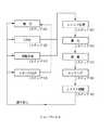
光学部材の姿勢変動の一例を図7に示す。図中に示すように、台形鏡1がθ方向に回転した場合、センサ20lとセンサ20rの台形鏡1との距離測定値にL・tanθの差が出てくる。ここにLは両センサ間の距離である。一方、プレート面上に転写される像は光学的に2θずれる。従って、この場合はプレートステージ9をプレートステージ回転駆動機構10にて2θだけ駆動させることにより、マスクのパターンはプレート上の正規の位置に転写されることになる。
【0010】
このように、センサ20l、20r、21u、21dにより台形鏡の姿勢を常時モニタし、この測定値を演算器30に通して補正すべき値を計算し、プレートステージスキャン駆動機構13ないしプレートステージ回転駆動機構10にそれぞれ必要な補正駆動司令を与えることで、各スキャン位置での台形鏡1の姿勢変動によるプレート面上での転写位置のずれを補正することができ、その結果プレート面全面に正確にマスクパターンが転写される。
【0011】
【実施例】
次に、本発明の実施例について図面を参照して説明する。
[実施例1]
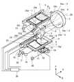
図1に本発明の一実施例に係る露光装置の構成を示す。同図において1、2、3は光学部材、4は照明系(不図示)によって照明されたスリット状の露光用照明光、5はマスク、6は半導体ウエハやガラス基板等のプレート、7はマスクステージスキャン駆動機構、8はマスクステージ、9はプレートステージ、10はプレートステージ回転機構、11はプレートステージX方向微動機構、12はプレートステージY方向微動機構、13はプレートステージスキャン駆動機構、14、25、26はレーザ干渉計、15、16、18は反射ミラー、17はビームスプリッタ、19a、19bはマスクパターン、19a’、19b’はプレート上に反転転写されたマスクパターン、20l、20r、21u、21dは台形鏡姿勢モニタセンサ、22はプレートステージの回転機構駆動モータ、23は光学部材の光学系中心軸、24a−1、24a−2、24a−3、24a−4、24a−5、24a−6は照明光4によって照明されたパターン19aがプレート6上に転写される時の光路、30は演算器である。
【0012】
上記構成において、露光用照明光4によって照明されたパターン19aは、光学部材1、2、3により反射されながら光路24a−1〜24a−6を経てプレート上の19a’に反転転写される。同様に、19bは19b’に反転転写される。一方、マスク5が固定されているマスクステージ8は、レーザ干渉計14の測定値を基にマスクステージスキャン駆動機構7によって定速駆動され、プレートステージ9はレーザ干渉計25の測定値を基に、マスクステージ8と同期駆動される。このように構成することにより、マスク全体のパターンがプレート上に左右反転した像として転写される。
【0013】
今、光学部材の一部、例えば台形鏡1が外部からの衝撃やスキャン中の振動でその姿勢が変動した場合、その光学部材をモニタしているセンサが変動の量及び方向を検知して、その情報を演算器30に送り込む。演算器30の中では、光学部材の動きがプレート6への転写精度に与える影響を計算し、その結果に基づいて転写精度への影響を補正する司令値をプレートステージ駆動機構であるプレートステージY方向微動機構12及び回転機構駆動モータ22へ与え、Y軸方向及びθ方向の補正駆動をさせる。結果として、露光中の光学部材の姿勢変動による転写像のずれを、露光中にプレートステージに前記補正駆動を加えることにより、転写精度を向上させることができる。
【0014】
[実施例2]
実施例1では、補正駆動をプレート側で行っているが、マスク(原版)側を駆動可能な構造にしてマスク(原版)側にて補正駆動しても同じ効果が得られる。
更に、光学部材をモニタすることにより該光学部材の位置が変動した場合には元の正規の位置に戻るよう、該光学部材を補正駆動させる機構を光学部材側に持たせても良い。
これらは単独でいずれかを行う(マスク、光学部材、プレートのいずれかのみ補正駆動する)形となるが、これらを組合わせて複合的に補正するようにしても良い。
【0015】
[デバイス生産方法の実施例]
次に上記説明した露光装置を利用したデバイスの生産方法の実施例を説明する。
図9は微小デバイス(ICやLSI等の半導体チップ、液晶パネル、CCD、薄膜磁気ヘッド、マイクロマシン等)の製造の流れを示す。ステップ1(回路設計)ではデバイスのパターン設計を行なう。ステップ2(マスク製作)では設計したパターンを形成したマスクを製作する。一方、ステップ3(ウエハ製造)ではシリコンやガラス等の材料を用いてウエハを製造する。ステップ4(ウエハプロセス)は前工程と呼ばれ、上記用意したマスクとウエハを用いて、リソグラフィ技術によってウエハ上に実際の回路を形成する。次のステップ5(組み立て)は後工程と呼ばれ、ステップ4によって作製されたウエハを用いて半導体チップ化する工程であり、アッセンブリ工程(ダイシング、ボンディング)、パッケージング工程(チップ封入)等の工程を含む。ステップ6(検査)ではステップ5で作製された半導体デバイスの動作確認テスト、耐久性テスト等の検査を行なう。こうした工程を経て半導体デバイスが完成し、これが出荷(ステップ7)される。
【0016】
図10は上記ウエハプロセスの詳細な流れを示す。ステップ11(酸化)ではウエハの表面を酸化させる。ステップ12(CVD)ではウエハ表面に絶縁膜を形成する。ステップ13(電極形成)ではウエハ上に電極を蒸着によって形成する。ステップ14(イオン打込み)ではウエハにイオンを打ち込む。ステップ15(レジスト処理)ではウエハに感光剤を塗布する。ステップ16(露光)では上記説明した露光装置によってマスクの回路パターンをウエハに焼付露光する。ステップ17(現像)では露光したウエハを現像する。ステップ18(エッチング)では現像したレジスト像以外の部分を削り取る。ステップ19(レジスト剥離)ではエッチングが済んで不要となったレジストを取り除く。これらのステップを繰り返し行なうことによって、ウエハ上に多重に回路パターンが形成される。
【0017】
本実施例の生産方法を用いれば、従来は製造が難しかった高集積度のデバイスを低コストに製造することができる。
【0018】
【発明の効果】
以上説明したように本発明は、光学部材の姿勢変動による転写像のずれを低減させることができる。
【図面の簡単な説明】
【図1】 本発明の一実施例に係る露光装置を示す要部概略図である。
【図2】 正規状態でのマスクパターンの転写を説明する図であり、(a)は平面図、(b)は側面図、(c),(d)は正面図である。
【図3】 光学部材の一部である台形鏡が回転した時の光路変化を説明する図であり、(a)は平面図、(b)は側面図である。
【図4】 光学部材の一部である台形鏡が傾いた時の光路変化を説明する図である。
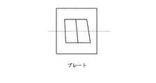
【図5】 光学部材の一部である台形鏡が回転した時のプレート上の転写パターンを説明する図である。
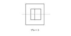
【図6】 光学部材の一部である台形鏡が傾いた時のプレート上の転写パターンを説明する図である。
【図7】 光学部材の一部である台形鏡が回転した場合のプレートステージでの補正を説明する図であり、(a)は要部概略図、(b),(c)は正面図である。
【図8】 従来の露光装置を示す要部概略図である。
【図9】 微小デバイスの製造の流れを示す図である。
【図10】 図9におけるウエハプロセスの詳細な流れを示す図である。
【符号の説明】
1,2,3:光学部材、1u:台形鏡上側反射面、1u’:台形鏡がθ回転した時の上側反射面、1d:台形鏡下側反射面、1d’:台形鏡がθ回転した時の下側反射面、4:露光用照明光、5:マスク、6:プレート、7:マスクステージスキャン駆動機構、8:マスクステージ、9:プレートステージ、10:プレートステージ回転駆動機構、11:プレートステージX方向微動機構、12:プレートステージY方向微動機構、13:プレートステージスキャン駆動機構、14,25,26:レーザ干渉計、15,16,18:反射ミラー、17:ビームスプリッタ、19a,19b:マスク上のパターン、19a’,19b’:プレート上転写パターン、20l,20r,21u,21d:台形鏡姿勢モニタセンサ、22:回転機構駆動モータ、23:光学系中心軸、24a−1,24a−2,24a−3,24a−4,24a−5,24a−6:光路、30:演算器。[0001]
BACKGROUND OF THE INVENTION
The present invention relates to an exposure apparatus used for manufacturing semiconductor devices and liquid crystal panels.
[0002]
[Prior art]
FIG. 8 shows a schematic diagram of a main part of a conventional exposure apparatus. As shown in the figure,
[0003]
On the other hand, the mask stage 8 holding the
[0004]
With this configuration, the pattern drawn on the mask is transferred onto the entire surface of the plate.
[0005]
[Problems to be solved by the invention]
In the conventional exposure apparatus, the
[0006]
Normally, in a state where the optical system is adjusted, as shown in FIG. 2, the pattern of the
[0007]
An object of the present invention is toreduce a shift of a transfer image due to such a change in posture of the optical member.
[0008]
[Means for Solving the Problems]
In order to achieve the above object, an exposure apparatus according to the present invention is an exposure apparatus having an imaging optical system that forms an image of a pattern formed on an original on a plate, and the posture of thetrapezoidal mirror in the imaging optical system isadjusted during exposure. Measuring means for measuring,and correcting at least one of the originalstage and the platestage based on the measurement result of the measuring meansso as to correct the shift of the transfer position on the plate surface due to the posture variation of the trapezoidal mirror One of the driving is performed.
[0009]
[Action]
An example of the posture variation of the optical member is shown in FIG. As shown in the figure, when the
[0010]
In this way, the attitude of the trapezoidal mirror is constantly monitored by the
[0011]
【Example】
Next, embodiments of the present invention will be described with reference to the drawings.
[Example 1]
FIG. 1 shows the arrangement of an exposure apparatus according to an embodiment of the present invention. In the figure, 1, 2 and 3 are optical members, 4 is a slit-shaped illumination light illuminated by an illumination system (not shown), 5 is a mask, 6 is a plate such as a semiconductor wafer or glass substrate, and 7 is a mask. Stage scan drive mechanism, 8 is a mask stage, 9 is a plate stage, 10 is a plate stage rotation mechanism, 11 is a plate stage X direction fine movement mechanism, 12 is a plate stage Y direction fine movement mechanism, 13 is a plate stage scan drive mechanism, 14, 25, 26 are laser interferometers, 15, 16, 18 are reflection mirrors, 17 are beam splitters, 19a, 19b are mask patterns, 19a ', 19b' are mask patterns reversely transferred onto the plate, 20l, 20r, 21u. , 21d is a trapezoidal mirror attitude monitor sensor, 22 is a plate stage rotation mechanism drive motor, and 23 is optical. 24a-1, 24a-2, 24a-3, 24a-4, 24a-5, 24a-6 are the optical system central axes of the material when the
[0012]
In the above configuration, the
[0013]
Now, when the posture of a part of the optical member, for example, the
[0014]
[Example 2]
In the first embodiment, correction driving is performed on the plate side. However, the same effect can be obtained even if correction driving is performed on the mask (original) side with a structure capable of driving the mask (original) side.
Furthermore, a mechanism for correcting and driving the optical member may be provided on the optical member side so that the optical member returns to the original normal position when the position of the optical member changes by monitoring the optical member.
These may be performed independently (only one of the mask, the optical member, and the plate is corrected and driven), but may be combined and corrected in combination.
[0015]
[Example of device production method]
Next, an embodiment of a device production method using the above-described exposure apparatus will be described.
FIG. 9 shows a flow of manufacturing a microdevice (a semiconductor chip such as an IC or LSI, a liquid crystal panel, a CCD, a thin film magnetic head, a micromachine, etc.). In step 1 (circuit design), a device pattern is designed. In step 2 (mask production), a mask on which the designed pattern is formed is produced. On the other hand, in step 3 (wafer manufacture), a wafer is manufactured using a material such as silicon or glass. Step 4 (wafer process) is called a pre-process, and an actual circuit is formed on the wafer by lithography using the prepared mask and wafer. The next step 5 (assembly) is referred to as a post-process, and is a process for forming a semiconductor chip using the wafer produced in
[0016]
FIG. 10 shows the detailed flow of the wafer process. In step 11 (oxidation), the wafer surface is oxidized. In step 12 (CVD), an insulating film is formed on the wafer surface. In step 13 (electrode formation), an electrode is formed on the wafer by vapor deposition. In step 14 (ion implantation), ions are implanted into the wafer. In step 15 (resist process), a photosensitive agent is applied to the wafer. In step 16 (exposure), the circuit pattern of the mask is printed onto the wafer by exposure using the exposure apparatus described above. In step 17 (development), the exposed wafer is developed. In step 18 (etching), portions other than the developed resist image are removed. In step 19 (resist stripping), unnecessary resist after etching is removed. By repeating these steps, multiple circuit patterns are formed on the wafer.
[0017]
By using the production method of this embodiment, a highly integrated device that has been difficult to manufacture can be manufactured at low cost.
[0018]
【The invention's effect】
As described above, the present invention canreduce the shift of the transferred image due to the change in the posture of the optical member .
[Brief description of the drawings]
FIG. 1 is a schematic view of the principal part showing an exposure apparatus according to an embodiment of the present invention.
2A and 2B are diagrams for explaining transfer of a mask pattern in a normal state, where FIG. 2A is a plan view, FIG. 2B is a side view, and FIG. 2C and FIG.
FIGS. 3A and 3B are views for explaining a change in optical path when a trapezoidal mirror that is a part of an optical member rotates, where FIG. 3A is a plan view and FIG. 3B is a side view;
FIG. 4 is a diagram for explaining an optical path change when a trapezoidal mirror that is a part of an optical member is tilted.
FIG. 5 is a diagram illustrating a transfer pattern on a plate when a trapezoidal mirror that is a part of an optical member rotates.
FIG. 6 is a diagram illustrating a transfer pattern on a plate when a trapezoidal mirror that is a part of an optical member is tilted.
FIGS. 7A and 7B are diagrams for explaining correction on a plate stage when a trapezoidal mirror that is a part of an optical member rotates, where FIG. 7A is a schematic view of the main part, and FIGS. is there.
FIG. 8 is a main part schematic diagram showing a conventional exposure apparatus.
FIG. 9 is a diagram showing a flow of manufacturing a microdevice.
10 is a diagram showing a detailed flow of the wafer process in FIG. 9; FIG.
[Explanation of symbols]
1, 2, 3: Optical member, 1u: trapezoidal mirror upper reflecting surface, 1u ′: upper reflecting surface when trapezoidal mirror is rotated by θ, 1d: trapezoidal mirror lower reflecting surface, 1d ′: trapezoidal mirror is rotated by θ Lower reflective surface at time, 4: exposure illumination light, 5: mask, 6: plate, 7: mask stage scan drive mechanism, 8: mask stage, 9: plate stage, 10: plate stage rotation drive mechanism, 11: Plate stage X direction fine movement mechanism, 12: Plate stage Y direction fine movement mechanism, 13: Plate stage scanning drive mechanism, 14, 25, 26: Laser interferometer, 15, 16, 18: Reflection mirror, 17: Beam splitter, 19a, 19b: Pattern on mask, 19a ', 19b': Transfer pattern on plate, 20l, 20r, 21u, 21d: Trapezoid mirror attitude monitor sensor, 22: Rotation mechanism drive mode , 23: optical system center axis, 24a-1,24a-2,24a-3,24a-4,24a-5,24a-6: light path, 30: operation unit.
Claims (3)
Translated fromJapanese露光中に前記結像光学系中の台形鏡の姿勢を測定する測定手段を有し、
前記台形鏡の姿勢変動による前記プレート面上での転写位置のずれを補正するように、前記測定手段の測定結果に基づいて原版ステージ、およびプレートステージのうちの少なくともいずれかの駆動を行うことを特徴とする露光装置。In an exposure apparatus having an imaging optical system that forms an image of a pattern formed on an original on a plate,
Measuring means for measuring the posture of thetrapezoidal mirror in the imaging optical system duringexposure ;
Driving at least one of the originalstage and the platestage based on the measurement result of the measuring meansso as to correct the shift of the transfer position on the plate surface due to the posture change of the trapezoidal mirror. A featured exposure apparatus.
Priority Applications (1)
| Application Number | Priority Date | Filing Date | Title |
|---|---|---|---|
| JP37088499AJP4521912B2 (en) | 1999-12-27 | 1999-12-27 | Exposure equipment |
Applications Claiming Priority (1)
| Application Number | Priority Date | Filing Date | Title |
|---|---|---|---|
| JP37088499AJP4521912B2 (en) | 1999-12-27 | 1999-12-27 | Exposure equipment |
Publications (3)
| Publication Number | Publication Date |
|---|---|
| JP2001185478A JP2001185478A (en) | 2001-07-06 |
| JP2001185478A5 JP2001185478A5 (en) | 2007-03-01 |
| JP4521912B2true JP4521912B2 (en) | 2010-08-11 |
Family
ID=18497768
Family Applications (1)
| Application Number | Title | Priority Date | Filing Date |
|---|---|---|---|
| JP37088499AExpired - Fee RelatedJP4521912B2 (en) | 1999-12-27 | 1999-12-27 | Exposure equipment |
Country Status (1)
| Country | Link |
|---|---|
| JP (1) | JP4521912B2 (en) |
Family Cites Families (6)
| Publication number | Priority date | Publication date | Assignee | Title |
|---|---|---|---|---|
| JPS61251030A (en)* | 1985-04-30 | 1986-11-08 | Canon Inc | projection exposure equipment |
| JP3429783B2 (en)* | 1992-01-07 | 2003-07-22 | 株式会社日立製作所 | Pattern exposure method and apparatus |
| JPH0878303A (en)* | 1994-08-31 | 1996-03-22 | Toshiba Corp | Correction prism device and exposure apparatus to which the same is applied |
| JPH08181063A (en)* | 1994-12-26 | 1996-07-12 | Nikon Corp | Aligner |
| JPH11325821A (en)* | 1998-05-19 | 1999-11-26 | Nikon Corp | Stage control method and exposure apparatus |
| TW490598B (en)* | 1999-11-30 | 2002-06-11 | Asm Lithography Bv | Lithographic projection apparatus and method of manufacturing a device using a lithographic projection apparatus |
- 1999
- 1999-12-27JPJP37088499Apatent/JP4521912B2/ennot_activeExpired - Fee Related
Also Published As
| Publication number | Publication date |
|---|---|
| JP2001185478A (en) | 2001-07-06 |
Similar Documents
| Publication | Publication Date | Title |
|---|---|---|
| KR0139039B1 (en) | Exposure apparatus and device manufacturing method using the same | |
| JP4434372B2 (en) | Projection exposure apparatus and device manufacturing method | |
| JP2000049066A (en) | Exposure apparatus and device manufacturing method | |
| KR100882046B1 (en) | Exposure apparatus and device manufacturing method | |
| JP3466893B2 (en) | Positioning apparatus and projection exposure apparatus using the same | |
| JP3335126B2 (en) | Surface position detecting apparatus and scanning projection exposure apparatus using the same | |
| JP2009099873A (en) | Exposure apparatus and device manufacturing method | |
| JP2010087310A (en) | Exposure apparatus, and method of manufacturing device | |
| JPH1140489A (en) | Projection exposure method and apparatus | |
| JP4521912B2 (en) | Exposure equipment | |
| JP3441930B2 (en) | Scanning exposure apparatus and device manufacturing method | |
| JP2000267732A (en) | Stage apparatus, exposure apparatus, and device manufacturing method | |
| JP2001059704A (en) | Positioning stage apparatus, semiconductor exposure apparatus, and device manufacturing method | |
| JPH09246168A (en) | Scanning exposure apparatus and method, and method of manufacturing device using the apparatus | |
| JPH11307436A (en) | Projection exposure apparatus, reticle, and reticle positioning method | |
| JPH09148236A (en) | Method and apparatus for controlling movement of substrate stage of exposure apparatus | |
| JP3722330B2 (en) | Exposure apparatus and device manufacturing method | |
| JP3198718B2 (en) | Projection exposure apparatus and method for manufacturing semiconductor device using the same | |
| JP3244872B2 (en) | Exposure apparatus and device manufacturing method using the same | |
| JP4378109B2 (en) | Exposure apparatus, projection optical system, and device manufacturing method | |
| JP2003059808A (en) | Exposure method and device manufacturing method | |
| JPH11354417A (en) | Scanning exposure apparatus, device manufacturing method using the same, and stage control apparatus | |
| JPH1187233A (en) | Projection exposure equipment | |
| JP3530716B2 (en) | Scanning projection exposure equipment | |
| KR102555768B1 (en) | Exposure method, exposure apparatus, method of manufacturing article, and measurement method |
Legal Events
| Date | Code | Title | Description |
|---|---|---|---|
| A521 | Request for written amendment filed | Free format text:JAPANESE INTERMEDIATE CODE: A523 Effective date:20061226 | |
| A621 | Written request for application examination | Free format text:JAPANESE INTERMEDIATE CODE: A621 Effective date:20061226 | |
| RD01 | Notification of change of attorney | Free format text:JAPANESE INTERMEDIATE CODE: A7421 Effective date:20090406 | |
| A977 | Report on retrieval | Free format text:JAPANESE INTERMEDIATE CODE: A971007 Effective date:20090821 | |
| A131 | Notification of reasons for refusal | Free format text:JAPANESE INTERMEDIATE CODE: A131 Effective date:20090901 | |
| A521 | Request for written amendment filed | Free format text:JAPANESE INTERMEDIATE CODE: A523 Effective date:20091028 | |
| RD04 | Notification of resignation of power of attorney | Free format text:JAPANESE INTERMEDIATE CODE: A7424 Effective date:20100201 | |
| TRDD | Decision of grant or rejection written | ||
| A01 | Written decision to grant a patent or to grant a registration (utility model) | Free format text:JAPANESE INTERMEDIATE CODE: A01 Effective date:20100511 | |
| A01 | Written decision to grant a patent or to grant a registration (utility model) | Free format text:JAPANESE INTERMEDIATE CODE: A01 | |
| A61 | First payment of annual fees (during grant procedure) | Free format text:JAPANESE INTERMEDIATE CODE: A61 Effective date:20100525 | |
| R150 | Certificate of patent or registration of utility model | Free format text:JAPANESE INTERMEDIATE CODE: R150 | |
| FPAY | Renewal fee payment (event date is renewal date of database) | Free format text:PAYMENT UNTIL: 20130604 Year of fee payment:3 | |
| LAPS | Cancellation because of no payment of annual fees |