JP4521399B2 - Drawing apparatus, drawing method, and drawing program - Google Patents
Drawing apparatus, drawing method, and drawing programDownload PDFInfo
- Publication number
- JP4521399B2 JP4521399B2JP2006519083AJP2006519083AJP4521399B2JP 4521399 B2JP4521399 B2JP 4521399B2JP 2006519083 AJP2006519083 AJP 2006519083AJP 2006519083 AJP2006519083 AJP 2006519083AJP 4521399 B2JP4521399 B2JP 4521399B2
- Authority
- JP
- Japan
- Prior art keywords
- pixels
- pixel
- processing unit
- pixel processing
- data
- Prior art date
- Legal status (The legal status is an assumption and is not a legal conclusion. Google has not performed a legal analysis and makes no representation as to the accuracy of the status listed.)
- Expired - Fee Related
Links
Images


Classifications
- G—PHYSICS
- G06—COMPUTING OR CALCULATING; COUNTING
- G06T—IMAGE DATA PROCESSING OR GENERATION, IN GENERAL
- G06T15/00—3D [Three Dimensional] image rendering
- G06T15/005—General purpose rendering architectures
Landscapes
- Engineering & Computer Science (AREA)
- Computer Graphics (AREA)
- Physics & Mathematics (AREA)
- General Physics & Mathematics (AREA)
- Theoretical Computer Science (AREA)
- Image Generation (AREA)
Description
Translated fromJapaneseこの発明は、描画装置、描画方法、及び描画プログラムに関するもので、例えば複数のピクセルを同時に並列処理する描画装置に関する。 The present invention relates to a drawing apparatus, a drawing method, and a drawing program, for example, a drawing apparatus that simultaneously processes a plurality of pixels in parallel.
近年、CPU(Central Processing Unit)の動作の高速化に伴って、画像描画装置に対しても高速化の要求が高まってきている。 In recent years, with the speeding up of the operation of a CPU (Central Processing Unit), there has been an increasing demand for speeding up image drawing apparatuses.
描画装置は、投入された図形をピクセルに分解するラスタライザと、ピクセルに描画処理を加えるピクセル処理部と、描画結果を読み書きするメモリとを備える。近年、CG(Computer Graphics)技術の進歩により、複雑なピクセル処理技術が頻繁に用いられるようになってきている。そのため、ピクセル処理部の負荷が大きく、そのためピクセル処理部を並列化することが行われている。更に、ピクセル処理部の並列度を上げるにつれて、処理速度のボトルネックは、メモリとの間のデータ転送となる。従って、データ転送バスを複雑化させることなく動作を高速化させるために、処理効率の向上のために、ピクセル処理部を並列化すると共に、各々のピクセル処理部にローカルメモリを割り当てる構成が、例えば特許第2901945号公報に提案されている。 The drawing apparatus includes a rasterizer that decomposes an input figure into pixels, a pixel processing unit that applies drawing processing to the pixels, and a memory that reads and writes drawing results. In recent years, with the advancement of CG (Computer Graphics) technology, complex pixel processing technology has been frequently used. Therefore, the load on the pixel processing unit is large, and therefore the pixel processing units are parallelized. Further, as the degree of parallelism of the pixel processing units is increased, the bottleneck of the processing speed becomes data transfer with the memory. Therefore, in order to increase the operation speed without complicating the data transfer bus, in order to improve the processing efficiency, the pixel processing units are parallelized, and a configuration in which a local memory is allocated to each pixel processing unit, for example, This is proposed in Japanese Patent No. 2901945.
しかしながら、上記手法であると、ピクセルの座標とピクセル処理部との対応が予め決まる。すなわち、ラスタライザは、各ピクセル処理部の処理状況を見て最も負荷の少ないピクセル処理部にピクセルを投入する、ということが出来ない。したがって、特定のピクセル処理部に負荷が集中することがあり、ピクセル処理部の負荷分散を均等にし難いという問題があった。そこで、各ピクセルに1つのピクセル処理部を対応させた構成も、例えばFuchs他著、“Fast Spheres, Shadows, Textures, Transparencies, and Image Enhancements in Pixel-Planes.”、Computer Graphics(Proc. SIGGRAPH 85)、Vol. 19、No. 3、p.111-120、1985年、及びFuchs他著、“Pixel-Planes 5: A Heterogeneous Multiprocessor Graphic System Using Processor-Enhanced Memories.”、Computer Graphics(Proc. SIGGRAPH 89)、Vol. 23、No.3、p.79-88、1989年に提案されている。 However, in the above method, the correspondence between the pixel coordinates and the pixel processing unit is determined in advance. In other words, the rasterizer cannot put pixels into the pixel processing unit with the least load in view of the processing status of each pixel processing unit. Therefore, there is a problem that the load is concentrated on a specific pixel processing unit, and it is difficult to evenly distribute the load of the pixel processing unit. Therefore, for example, Fuchs et al., “Fast Spheres, Shadows, Textures, Transparencies, and Image Enhancements in Pixel-Planes.”, Computer Graphics (Proc. SIGGRAPH 85) , Vol. 19, No. 3, p. 111-120, 1985, and Fuchs et al., “Pixel-Planes 5: A Heterogeneous Multiprocessor Graphic System Using Processor-Enhanced Memories.”, Computer Graphics (Proc. SIGGRAPH 89) , Vol. 23, No. 3, p. 79-88, proposed in 1989.
しかしながら、上記文献記載の方法であると、描画装置が非常に大規模にならざるを得ず、現実的でないという問題があった。 However, in the method described in the above document, there is a problem that the drawing apparatus has to be very large and is not realistic.
本発明は、回路規模を大型化することなく画像処理効率を向上出来る描画装置、描画方法、及び描画プログラムを提供する。This onsetMing, drawing apparatus can improve image processing efficiency without increasing the size of the circuit scale,that provides a drawing method, and drawingprograms.
この発明の一態様に係る描画装置は、図形の描画領域をマトリクス状に分割して得られる複数のピクセルのうち、描画すべき図形に応じたピクセルを生成するラスタライザと、前記ラスタライザによって生成された前記ピクセルに対して描画処理を行うN個(N=2(2n+2)、nは1以上の自然数)のピクセル処理部と、前記ピクセル処理部毎に設けられ、対応する前記ピクセル処理部によって描画された前記ピクセルのデータを保持する複数のメモリと、を具備し、前記ピクセル処理部は、複数の前記ピクセルに対して描画処理を行い、同一の前記ピクセル処理部によって描画処理される前記ピクセル同士は、前記描画領域内において等距離且つ等方的に位置し、同一の前記ピクセル処理部によって描画される近接する3つの前記ピクセルは、前記描画領域において、三辺のうちで最も短い辺の長さがN1/2より大きい三角形を形成する。A drawing apparatus according toan aspect of the present invention includes a rasterizer that generates pixels corresponding to a figure to be drawn among a plurality of pixels obtained by dividing a drawing area of the figure into a matrix, and the rasterizer generated by the rasterizerN pixel processingunits that perform rendering processing on the pixels(N = 2(2n + 2), where n is a natural number greater than or equal to 1)and each pixel processing unit, and are rendered by the corresponding pixel processing unit. A plurality of memories for storing data of the pixels, wherein the pixel processing unit performs drawing processing on the plurality of pixels, and the pixels to be drawn by the same pixel processing unit are the drawing area smelllike distance and isotropicallylocatedTe, three of the pins adjacent drawn by the same the pixel processing unit Cell in the drawing area, the length of the shortest side among the three sidestoform aN1/2larger triangle.
更に、この発明の一態様に係る描画方法は、図形の描画領域をマトリクス状に分割して得られる複数のピクセルのうち、描画すべき図形に応じたピクセルを生成するラスタライザを用いた描画方法であって、図形情報に基づいてピクセルを生成するステップと、生成されたピクセルが描画領域内において占める位置に応じて、N個(N=2(2n+2)、nは1以上の自然数)のうちの対応するピクセル処理部に前記ピクセルを投入するステップと、投入されたピクセルに対して描画処理を行うステップと、描画処理を行ったピクセルデータを、前記ピクセル処理部に対応して設けられたメモリに格納するステップとを具備し、前記ラスタライザは、同一の前記ピクセル処理部によって描画処理される前記ピクセル同士が、前記描画領域内において等距離且つ等方的に位置し、且つ同一の前記ピクセル処理部によって描画される近接する3つの前記ピクセルが、前記描画領域において、三辺のうちで最も短い辺の長さがN1/2より大きい三角形を形成するように、前記ピクセル処理部に前記ピクセルを投入する。Furthermore, a drawing method according to an aspect of the present invention isa drawing method using a rasterizer that generates pixels corresponding to a figure to be drawn among a plurality of pixels obtained by dividing a drawing area of thefigure into a matrix. According to the step of generating a pixel based onthe graphic information and the position occupied by the generated pixel in the drawing area, N (N = 2(2n + 2) , where n is a natural number of 1 or more) A step of inputting the pixel into a corresponding pixel processing unit, a step of performing a drawing process on the input pixel, and a pixel data subjected to the drawing process in a memory provided corresponding to the pixel processing unit; And storing the pixels in the rendering area so that the pixels to be rendered by the same pixel processing unit are within the rendering area. Oite equidistant and isotropically located, and three of the pixels adjacent drawn by the same the pixel processing unit, in the drawing area, the length of the shortest side among the three sides is N1 The pixels are input to the pixel processing unit so as to form a triangle larger than/ 2 .
更に、この発明の一態様に係る描画プログラムは、図形を描画するためにコンピュータを、入力された図形情報に応じたピクセルを生成するピクセル生成手段と、各々が、前記ピクセル生成手段によって生成された前記ピクセルのうち、描画領域内において実質的に等距離且つ等方的に位置する複数の前記ピクセルについて描画処理を行う複数の描画手段と、前記描画手段によって描画された前記ピクセルのデータを保持するN個(N=2(2n+2)、nは1以上の自然数)の保持手段として機能させ、同一の前記保持手段によって保持される近接する3つの前記ピクセルは、前記描画領域において、三辺のうちで最も短い辺の長さがN1/2より大きい三角形を形成する。Furthermore, a drawing program according to one aspect of the present invention includes a computer for drawing a graphic, pixel generation means for generating pixels according to input graphic information, and each of the pixel generation means generated by the pixel generation means. Among the pixels, a plurality of drawing means for performing drawing processing on a plurality of the pixels that are located at substantially equal distance and isotropic in the drawing area, and hold data of the pixels drawn by the drawing meansn pieces(n = 2 (2n + 2 ), nis a natural number of 1 or more) to serve asa retainingmeans, three of the pixels proximate held by the same said retaining means, in the drawing area, the three sides of the the length of the shortest side is thatto form theN1/2largertriangleout.
この発明の第1の実施形態に係る描画装置について、図1を用いて説明する。図1は、本実施形態に係る画像描画プロセッサシステムLSIのブロック図である。 A drawing apparatus according to a first embodiment of the present invention will be described with reference to FIG. FIG. 1 is a block diagram of an image drawing processor system LSI according to the present embodiment.
図示するように、本実施形態に係る画像描画プロセッサシステムLSI10は、ホストプロセッサ20、I/Oプロセッサ30、メインメモリ40、及びグラフィックプロセッサ50を備えている。ホストプロセッサ20とグラフィックプロセッサ50とは、プロセッサバスBUSによって、相互に通信可能に接続されている。 As illustrated, the image drawing processor system LSI 10 according to the present embodiment includes a
ホストプロセッサ20は、メインプロセッサ21、I/O部22〜24、及び複数の信号処理部(DSP:Digital Signal Processor)25を備えている。これらの回路ブロックは、ローカルネットワークLN1によって相互に通信可能に接続されている。メインプロセッサ21は、ホストプロセッサ20内の各回路ブロックの動作を制御する。I/O部22は、I/Oプロセッサ30を介してホストプロセッサ20外部とデータの授受を行う。I/O部23は、メインメモリ40との間でデータの授受を行う。I/O部24は、プロセッサバスBUSを介してグラフィックプロセッサ50との間でデータの授受を行う。信号処理部25は、メインメモリ40や外部から読み込んだデータに基づいて信号処理を行う。 The
I/Oプロセッサ30は、ホストプロセッサ20と、例えば汎用バス、HDDやDVD(Digital Versatile Disc)ドライブ等の周辺機器並びにネットワークとを接続する。この際、HDDやDVDドライブは、LSI10に搭載されているものでも良いし、またはLSI10外部に設けられていても良い。 The I /
メインメモリ40は、ホストプロセッサ20が動作するために必要なプログラムを保持する。このプログラムは、例えば図示せぬHDD等から読み出されて、メインメモリ40に格納される。 The
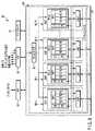
グラフィックプロセッサ50は、コントローラ51、I/O部52、53、演算処理部54を備えている。コントローラ51は、ホストプロセッサ20との間の通信や、演算処理部54の制御を行う。I/O部52は、プロセッサバスBUSを介したホストプロセッサ20との間の入出力を司る。I/O部53は、PCI等の各種汎用バス、ビデオ及びオーディオ、更に外部メモリ等との入出力を司る。演算処理部54は、画像処理演算を行う。 The
演算処理部54は、ラスタライザ(rasterizer)55、及び複数の信号処理部56−0〜56−31を備えている。なお、本実施形態では信号処理部56の数を32個にしているが、これは一例に過ぎず、8個、16個、64個等でも良く、その数は限定されるものではない。演算処理部54の詳細な構成について、図2を用いて説明する。図2はグラフィックプロセッサ50のブロック図である。 The
図示するように、演算処理部54は、ラスタライザ55と、32個の信号処理部56−0〜56−31を備えている。ラスタライザ55は、入力された図形情報に従って、ピクセル(pixel)を生成する。ピクセルとは、所定の図形を描画する際に取り扱われる最小単位の領域のことであり、ピクセルの集合によって図形が描画される。生成されるピクセルは、図形の形状(図形の占める位置)によって決まっている。すなわち、ある位置を描画する際にはその位置に対応したピクセルが生成され、また別の位置を描画する際には、対応する別のピクセルが生成される。信号処理部56−0〜56−31はそれぞれ、ピクセル処理部PPU0〜PPU31、及びピクセル処理部毎に設けられたローカルメモリLM0〜LM31を含んでいる。 As illustrated, the
ピクセル処理部PPU0〜PPU31はそれぞれ、4個のリアライズパイプRP(realize pipe)を有しており、4個のリアライズパイプRPが1個のRPクラスタRPC(realize pipe cluster)を形成している。RPクラスタRPCのそれぞれは、SIMD(Single Instruction Multiple Data)動作を行って、4個のピクセルを同時に処理する。そして、図形のそれぞれの位置に対応するピクセルは各ピクセル処理部PPU0〜PPU31に割り当てられており、図形の占める位置に応じて、対応するピクセル処理部PPU0〜PPU31がピクセルを処理する。ピクセルの位置とピクセル処理部との関係は後に詳述する。 Each of the pixel processing units PPU0 to PPU31 has four realize pipes RP (realize pipe), and the four realize pipes RP form one RP cluster RPC (realize pipe cluster). Each of the RP clusters RPC performs SIMD (Single Instruction Multiple Data) operation to process four pixels simultaneously. The pixels corresponding to the respective positions of the graphic are allocated to the pixel processing units PPU0 to PPU31, and the corresponding pixel processing units PPU0 to PPU31 process the pixels according to the positions occupied by the graphic. The relationship between the pixel position and the pixel processing unit will be described in detail later.
ローカルメモリLM0〜LM31はそれぞれ、ピクセル処理部PPU0〜PPU31によって生成されたピクセルデータを記憶する。ローカルメモリLM0〜LM31は、全体としてリアライズメモリ(realize memory)を形成する。リアライズメモリは、例えば1つのDRAMであり、その内の所定のデータ幅を有する各メモリ領域が、それぞれローカルメモリLM0〜LM31に相当する。 The local memories LM0 to LM31 store pixel data generated by the pixel processing units PPU0 to PPU31, respectively. The local memories LM0 to LM31 form a realize memory as a whole. The realization memory is, for example, one DRAM, and each memory area having a predetermined data width corresponds to the local memories LM0 to LM31, respectively.
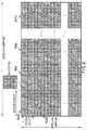
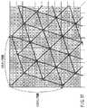
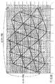
次に、本実施形態に係るグラフィックプロセッサにおける、ピクセルと描画位置との関係について図3を用いて説明する。図3は、図形を描画すべき全体の空間を示す概念図である。なお、図3に示す描画領域は、ローカルメモリ内においてピクセルデータを保持するメモリ空間(以下、フレームバッファ(frame buffer)と呼ぶ)に相当する。 Next, the relationship between the pixel and the drawing position in the graphic processor according to the present embodiment will be described with reference to FIG. FIG. 3 is a conceptual diagram showing the entire space in which a figure is to be drawn. The drawing area shown in FIG. 3 corresponds to a memory space (hereinafter referred to as a frame buffer) that holds pixel data in the local memory.
図示するように、フレームバッファは、マトリクス状に配置された((m+1)×(l+1))個のブロックBLK0〜BLKnを含んでいる。図3ではl=29、m=19
、n=599の場合について示しているが、この数は一例に過ぎず、限定されるものではない。ピクセル処理部PPU0〜PPU31は、ブロックBLK0〜BLK599順にピクセルを生成する。各ブロックBLK0〜BLK599はそれぞれ、マトリクス状に配置された32個のスタンプS(stamp)を含んで形成されている。図4は、図3に示された各ブロックが複数のスタンプを有する様子を示している。As shown in the figure, the frame buffer includes ((m + 1) × (l + 1)) blocks BLK0 to BLKn arranged in a matrix. In FIG. 3, l = 29, m = 19
, N = 599, but this number is only an example and is not limited. Pixel processing units PPU0 to PPU31 generate pixels in the order of blocks BLK0 to BLK599. Each of the blocks BLK0 to BLK599 is formed to include 32 stamps S (stamp) arranged in a matrix. FIG. 4 shows how each block shown in FIG. 3 has a plurality of stamps.
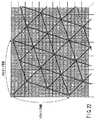
図示するように、各スタンプは、同一のピクセル処理部によって描画される複数のピクセルの集合体である。本実施形態では1個のスタンプは(4×4)=16個のピクセルを含んでいるが、この数は例えば1個、4個、…等でも良く、限定されるものではない。図4において各スタンプに記載された番号S(=0〜31)を、以下スタンプIDと呼ぶ。そしてスタンプIDは、当該スタンプ内のピクセルを描画するピクセル処理部の番号に一致する。従って、スタンプIDとしてS=0が割り当てられたスタンプ内のピクセルはピクセル処理部PPU0によって描画され、S=31が割り当てられたスタンプ内のピクセルはピクセル処理部PPU31によって描画される。 As shown in the figure, each stamp is an aggregate of a plurality of pixels drawn by the same pixel processing unit. In this embodiment, one stamp includes (4 × 4) = 16 pixels, but this number may be one, four,..., For example, and is not limited. The number S (= 0 to 31) described in each stamp in FIG. 4 is hereinafter referred to as a stamp ID. The stamp ID matches the number of the pixel processing unit that draws the pixels in the stamp. Accordingly, the pixels in the stamp assigned S = 0 as the stamp ID are drawn by the pixel processing unit PPU0, and the pixels in the stamp assigned S = 31 are drawn by the pixel processing unit PPU31.
ブロックBLK0〜BLK599の各々には、上記スタンプが(8×4)=32個含まれている。1つのブロックに含まれる32個のスタンプは、全て異なるピクセル処理部によって描画される。従って、1つのブロックあたりのスタンプ数は、ピクセル処理部数に等しい。そして、ブロック内においてスタンプは、左上から右下に向かって、S=0からS=31まで順次割り当てられている。すなわち、左上から水平方向に並ぶ2つのスタンプが2段設けられ、この(2×2)個のスタンプが水平方向に2つ並び、この(4×2)個のスタンプが2段設けられ、この(4×4)個のスタンプが水平方向に2つ並んでいる。そして各スタンプは、この順序に従って、それぞれピクセル処理部PPU0〜PPU31によって描画される。換言すれば、この順序に従ってスタンプIDが割り付けられる。但し、各スタンプへのIDの割り当ては任意であり、上記方法には限られない。すなわち、1つのブロックにピクセル処理部数と等しい数のスタンプが含まれ、それらのスタンプの全てが、互いに異なるピクセル処理部によって処理されるものであれば良い。従って、全体として(640×480)個のピクセルによって、図形を描画すべき空間が形成されている。また、同一ピクセル処理部によって処理される最近接の3つのスタンプは、直角三角形を形作るようにして位置している(図4では、ピクセル処理部PPU0によって処理されるスタンプS=0が、直角三角形の頂点に位置している様子を示している)。Each of the blocks BLK0 to BLK599 includes (8 × 4) = 32 stamps. All 32 stamps included in one block are drawn by different pixel processing units. Therefore, the number of stamps per block is equal to the number of pixel processing units. In the block, stamps are sequentially assigned from S = 0 to S = 31 from the upper left to the lower right. That is, two stages of two stamps arranged in the horizontal direction from the upper left are provided, two of these (2 × 2) stamps are arranged in the horizontal direction, and two stages of these (4 × 2) stamps are provided. Two (4 × 4) stamps are arranged in the horizontal direction. Each stamp is drawn by the pixel processing units PPU0 to PPU31 in this order. In other words, stamp IDs are assigned according to this order. However, the assignment of the ID to each stamp is arbitrary and is not limited to the above method. That is, it is sufficient if one block includes the same number of stamps as the number of pixel processing units, and all of these stamps are processed by different pixel processing units. Whatslave, the whole (640 × 480) pieces of pixels, the space to be drawn shapes are formed. The three closest stamps processed by the same pixel processing unit are positioned so as to form a right triangle (in FIG. 4, the stamp S = 0 processed by the pixel processing unit PPU0 is a right triangle). Is shown at the top).
次に、図2に示すグラフィックプロセッサ50の動作について、図5を用いて説明する。図5は、図形描画時におけるグラフィックプロセッサ50の動作を示すフローチャートである。 Next, the operation of the
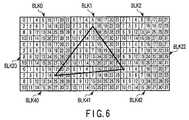
まず図形を描画するにあたって、まずラスタライザ55に図形情報が入力される(ステップS10)。図形情報は、例えば図形の頂点座標や色情報などである。ここで、例として三角形を描画する場合について説明する。ラスタライザ55に入力された三角形は、描画空間において、図6に示すような位置を占めるとする。すなわち、三角形の3つの頂点座標が、ブロックBLK1のスタンプS=7、ブロックBLK40のスタンプS=19、及びブロックBLK42のスタンプS=0に相当すると仮定する。 First, when drawing a graphic, graphic information is first input to the rasterizer 55 (step S10). The graphic information is, for example, the vertex coordinates or color information of the graphic. Here, a case where a triangle is drawn will be described as an example. It is assumed that the triangles input to the
すると、ラスタライザ55は描画すべき三角形が占める位置に対応するスタンプ(またはピクセル)を生成する(ステップS11)。この様子を示しているのが図7である。生成されたスタンプデータは、それぞれ予め対応付けられたピクセル処理部PPU0〜PPU31に送られる(ステップS12)。 Then, the
そして、入力されたスタンプデータに基づいて、ピクセル処理部が自らの担当するピクセルについて描画処理を行う(ステップS13)。図7の例であると、ブロックBLK1について、ピクセル処理部PPU7、PPU11〜PPU15、PPU24、PPU26、PPU27が、それぞれが担当するピクセルについて描画処理を行う。ブロックBLK20については、ピクセル処理部PPU29〜PPU31が、それぞれが担当するピクセルについて描画処理を行う。ブロックBLK21については、ピクセル処理部PPU1〜PPU19、PPU22、PPU24〜PPU31が、それぞれが担当するピクセルについて描画処理を行う。ブロックBLK40については、ピクセル処理部PPU19〜PPU23が、それぞれが担当するピクセルについて描画処理を行う。ブロックBLK41については、ピクセル処理部PPU0〜PPU7、PPU16〜PPU18、PPU20、PPU21が、それぞれが担当するピクセルについて描画処理を行う。 Then, based on the input stamp data, the pixel processing unit performs a drawing process for the pixels that it is responsible for (step S13). In the example of FIG. 7, for the block BLK1, the pixel processing units PPU7, PPU11 to PPU15, PPU24, PPU26, and PPU27 perform drawing processing on the pixels that they are responsible for. For the block BLK20, the pixel processing units PPU29 to PPU31 perform drawing processing for the pixels that they are responsible for. For the block BLK21, the pixel processing units PPU1 to PPU19, PPU22, and PPU24 to PPU31 perform drawing processing for the pixels that they are responsible for. For the block BLK40, the pixel processing units PPU19 to PPU23 perform drawing processing for the pixels that they are responsible for. For the block BLK41, the pixel processing units PPU0 to PPU7, PPU16 to PPU18, PPU20, and PPU21 perform drawing processing for the pixels that they are responsible for.
以上の結果、図7に示されるような三角形が、複数のピクセルによって描画される。ピクセル処理部によって描画されたピクセルデータは、スタンプ単位でローカルメモリLM0〜LM31に格納される(ステップS14)。前述の通り、ピクセル処理部PPU0〜PPU31のそれぞれはローカルメモリLM0〜LM31に対応しており、ピクセル処理部PPU0〜PPU31によって処理されたピクセルデータは、それぞれローカルメモリLM0〜LM31に格納される。 As a result, a triangle as shown in FIG. 7 is drawn by a plurality of pixels. The pixel data drawn by the pixel processing unit is stored in the local memories LM0 to LM31 in units of stamps (step S14). As described above, each of the pixel processing units PPU0 to PPU31 corresponds to the local memories LM0 to LM31, and the pixel data processed by the pixel processing units PPU0 to PPU31 are stored in the local memories LM0 to LM31, respectively.
上記のように、本実施形態に係る描画装置によれば、フレームバッファは複数のスタンプを有する複数のブロックが集まって形成されている。そして、個々のブロック内のスタンプは、それぞれ異なるピクセル処理部PPU0〜PPU31によって処理される。この際、同一ピクセル処理部によって処理される最近接の3つのスタンプは、直角三角形の頂点にそれぞれ位置する。 As described above, according to the drawing apparatus according to the present embodiment, the frame buffer is formed by collecting a plurality of blocks having a plurality of stamps. The stamps in the individual blocks are processed by different pixel processing units PPU0 to PPU31. At this time, the three closest stamps processed by the same pixel processing unit are respectively located at the vertices of the right triangle.
以上のようにしてスタンプをフレームバッファ内に配置することで、ピクセル処理部PPU0〜PPU31の負荷を、従来に比べて均等に分散させることが出来る。その結果、ピクセルの座標とピクセル処理部との対応が予め決まる、各々のピクセル処理部にローカルメモリを割り当てる構成において、特に回路規模を大型化することなく、描画処理を高速化することが出来る。 By placing the stamp in the frame buffer as described above, the load on the pixel processing units PPU0 to PPU31 can be evenly distributed as compared with the conventional case. As a result, in the configuration in which the correspondence between the pixel coordinates and the pixel processing unit is determined in advance and a local memory is allocated to each pixel processing unit, the drawing process can be speeded up without particularly increasing the circuit scale.
次に、この発明の第2の実施形態に係る描画装置について図8を用いて説明する。本実施形態は、上記第1の実施形態で説明したスタンプの配置をテクスチャにも適用したものである。図8は、本実施形態に係る画像描画プロセッサシステムLSI10の備えるグラフィックプロセッサ50のブロック図である。 Next, a drawing apparatus according to a second embodiment of the present invention will be described with reference to FIG. In the present embodiment, the stamp arrangement described in the first embodiment is also applied to the texture. FIG. 8 is a block diagram of the
図示するように、本実施形態に係るグラフィックプロセッサ50は、上記第1の実施形態で説明した構成において、信号処理部56−0〜56−31のそれぞれが、テクスチャユニットTU(texture unit)及び読み出し回路RCを更に有している。そしてローカルメモリLM0〜LM31のそれぞれは、参照画像(テクスチャ:texture)データを保持する。 As illustrated, in the
読み出し回路RCは、ローカルメモリLM0〜LM31からテクスチャデータを読み出す。テクスチャユニットTUは、テクスチャ処理を行う。すなわち、読み出し回路RCによって読み出したテクスチャデータを、ピクセル処理部で処理中のピクセルに貼り付ける(以下、この処理をテクスチャマッピング(texture mapping)という)。 The read circuit RC reads texture data from the local memories LM0 to LM31. The texture unit TU performs texture processing. That is, the texture data read by the read circuit RC is pasted to the pixel being processed by the pixel processing unit (hereinafter, this process is referred to as texture mapping).
図9はテクスチャデータの一例を示す概念図である。図示するように、テクスチャデータは、マトリクス状に配置された((m+1)×(l+1))個のテクスチャブロックTBLK0〜TBLKnを含んでいる。図9ではl=29、m=19、n=599個の場合について示しているが、この数は一例に過ぎず、限定されるものではない。 FIG. 9 is a conceptual diagram showing an example of texture data. As illustrated, the texture data includes ((m + 1) × (l + 1)) texture blocks TBLK0 to TBLKn arranged in a matrix. Although FIG. 9 shows the case of l = 29, m = 19, and n = 599, this number is only an example and is not limited.
テクスチャブロックTBLK0〜TBLKnのそれぞれは、(8×4)=32個のテクスチャスタンプ(texture stamp)を含んでいる。そして各テクスチャスタンプは、同一のローカルメモリに格納される複数のテクセル(texel)の集合体である。テクセルとは、所定のテクスチャを取り扱う際の最小単位であり、テクセルの集合によって、テクスチャが形成される。本実施形態では1個のテクスチャスタンプは(4×4)=16個のテクセルを含んでいるが、この数は例えば1個、4個、…などでも良く、限定されるものではない。但し、スタンプを形成するピクセル数と、テクスチャスタンプを形成するテクセル数とは等しいことが望ましい。図9において各スタンプに記載された番号T(0〜31)を、以下テクスチャスタンプIDと呼ぶ。そしてテクスチャスタンプIDは、当該テクスチャスタンプ内のテクセルを格納するローカルメモリの番号に一致する。従って、テクスチャスタンプIDとしてT=0が割り当てられたテクスチャスタンプ内のテクセルはローカルメモリLM0に格納され、T=31が割り当てられたテクスチャスタンプ内のテクセルはローカルメモリLM31に格納される。 Each of the texture blocks TBLK0 to TBLKn includes (8 × 4) = 32 texture stamps. Each texture stamp is an aggregate of a plurality of texels stored in the same local memory. A texel is a minimum unit for handling a predetermined texture, and a texture is formed by a set of texels. In this embodiment, one texture stamp includes (4 × 4) = 16 texels, but this number may be one, four,..., For example, and is not limited. However, it is desirable that the number of pixels forming the stamp is equal to the number of texels forming the texture stamp. In FIG. 9, the number T (0 to 31) described in each stamp is hereinafter referred to as a texture stamp ID. The texture stamp ID matches the number of the local memory that stores the texels in the texture stamp. Accordingly, the texels in the texture stamp assigned with T = 0 as the texture stamp ID are stored in the local memory LM0, and the texels in the texture stamp assigned with T = 31 are stored in the local memory LM31.
なお図9において斜線が付されているのは、何らかの絵柄が描かれていることを示すためであり、フレームバッファと区別するためのものである。 In FIG. 9, the hatched lines are used to indicate that a certain pattern is drawn, and are used for distinguishing from the frame buffer.
そして、1つのテクスチャブロックに含まれる32個のテクスチャスタンプデータは、全て異なるローカルメモリに格納される。従って、1つのテクスチャブロックあたりのテクスチャスタンプ数は、ローカルメモリ数(=ピクセル処理部数)に等しい。そして、テクスチャブロック内においてテクスチャスタンプは、左上から右下に向かって、T=0からT=31まで順次割り当てられている。すなわち、左上から水平方向に並ぶ2つのテクセルが2段設けられ、この(2×2)個のテクセルが水平方向に2つ並び、この(4×2)個のテクセルが2段設けられ、この(4×4)個のテクセルが水平方向に2つ並んでいる。そして各テクスチャスタンプは、この順序に従って、それぞれローカルメモリLM0〜LM31に格納される。換言すれば、この順序に従ってIDが割り付けられる。従って、全体として(640×480)個のテクスチャスタンプによってテクスチャデータが形成されている。また、同一IDを有する最近接の3つのテクセルは、直角三角形を形作るようにして位置している。 The 32 texture stamp data included in one texture block are all stored in different local memories. Therefore, the number of texture stamps per texture block is equal to the number of local memories (= the number of pixel processing units). In the texture block, texture stamps are sequentially assigned from T = 0 to T = 31 from the upper left to the lower right. That is, two texels arranged in the horizontal direction from the upper left are provided in two stages, two (2 × 2) texels are arranged in the horizontal direction, and two (4 × 2) texels are provided in this stage. Two (4 × 4) texels are arranged in the horizontal direction. Each texture stamp is stored in the local memories LM0 to LM31 in this order. In other words, IDs are assigned according to this order. Therefore, the texture data is formed by (640 × 480) texture stamps as a whole. The three closest texels having the same ID are positioned so as to form a right triangle.
以上のように、テクスチャデータは、上記第1の実施形態で説明したフレームバッファと同様の方法によって、IDが割り付けられている。各テクスチャスタンプへのIDの割り当ては任意であり、上記方法には限られない。すなわち、1つのテクスチャブロックにローカルメモリ数と等しい数のテクスチャスタンプが含まれ、それらのテクスチャスタンプの全てが、互いに異なるローカルメモリによって保持されるものであれば良い。但し、フレームバッファのスタンプと同じようにIDが割り当てられることが望ましい。 As described above, the texture data is assigned an ID by the same method as the frame buffer described in the first embodiment. The assignment of the ID to each texture stamp is arbitrary and is not limited to the above method. That is, the number of texture stamps equal to the number of local memories is included in one texture block, and all the texture stamps may be held by different local memories. However, it is desirable to assign an ID in the same way as the frame buffer stamp.
次に、図8に示すグラフィックプロセッサ50の動作について、図10を用いて説明する。図形を描画する方法は、基本的には上記第1の実施形態で説明したとおりである。すなわち、まずラスタライザ55に図形情報が入力される(ステップS10)。ここでは、第1の実施形態と同様に、図6に示す三角形を描画する場合について説明する。 Next, the operation of the
次にラスタライザ55は、描画すべき三角形が占める位置に対応するスタンプ(またはピクセル)を生成する(ステップS11)。この様子は図7に示す通りである。生成されたスタンプデータは、それぞれ予め対応付けられたピクセル処理部PPU0〜PPU31に送られる(ステップS12)。 Next, the
そして、入力されたスタンプデータに基づいて、ピクセル処理部が自らの担当するピクセルについて描画処理を行う。同時に、描画した図形にテクスチャデータを貼り付けるテクスチャマッピングを行う(ステップS20)。以下テクスチャマッピングについて詳述する。 Then, based on the input stamp data, the pixel processing unit performs a drawing process for the pixels that it is responsible for. At the same time, texture mapping is performed in which texture data is pasted on the drawn figure (step S20). The texture mapping will be described in detail below.
信号処理部56−0〜56−31は、ピクセル処理部PPU0〜PPU31によってピクセルに対する描画処理を行うと共に、読み出し回路RCによって、対応するピクセルに貼り付けるべきテクスチャデータをローカルメモリLM0〜LM31から読み出す。例えば、ピクセル処理部が図7に示す三角形を描画するとする。そして、図7に示す三角形に貼り付けるテクスチャデータは、図11に示すように、テクスチャブロックTBLK1、TBLK20、TBLK21、TBLK41にまたがる三角形であったとする。そして、フレームバッファにおけるブロックBLK1、スタンプS=7に位置する頂点が、テクスチャにおけるテクスチャブロックTBLK20、テクスチャスタンプT=21に対応し、フレームバッファにおけるブロックBLK40、スタンプS=19に位置する頂点が、テクスチャにおけるテクスチャブロックTBLK41、テクスチャスタンプT=30に対応し、フレームバッファにおけるブロックBLK42、スタンプS=0に位置する頂点が、テクスチャにおけるテクスチャブロックTBLK1、テクスチャスタンプT=20に対応すると仮定する。 The signal processing units 56-0 to 56-31 perform drawing processing on the pixels by the pixel processing units PPU0 to PPU31, and read out the texture data to be pasted to the corresponding pixels from the local memories LM0 to LM31 by the reading circuit RC. For example, assume that the pixel processing unit draws a triangle shown in FIG. Then, it is assumed that the texture data pasted on the triangle shown in FIG. 7 is a triangle extending over the texture blocks TBLK1, TBLK20, TBLK21, and TBLK41 as shown in FIG. The vertex located in the block BLK1 and stamp S = 7 in the frame buffer corresponds to the texture block TBLK20 and texture stamp T = 21 in the texture, and the vertex located in block BLK40 and stamp S = 19 in the frame buffer is the texture. Assume that the texture block TBLK41 and texture stamp T = 30 correspond to the vertex located at the block BLK42 and stamp S = 0 in the frame buffer correspond to the texture block TBLK1 and texture stamp T = 20 in the texture.
すると、信号処理部56−7の読み出し回路RCは、ローカルメモリLM21からテクスチャブロックTBLK20のテクスチャスタンプT=21に対応するテクセルデータを読み出す。すると信号処理部56−7のテクスチャユニットTUが、ブロックBLK1のスタンプS=7に、テクスチャブロックTBLK20のテクスチャスタンプT=21を貼り付ける。また信号処理部56−19の読み出し回路RCは、ローカルメモリLM30からテクスチャブロックTBLK41のテクスチャスタンプT=30に対応するテクセルデータを読み出す。すると信号処理部56−19のテクスチャユニットTUが、ブロックBLK40のスタンプS=19に、テクスチャブロックTBLK41のテクスチャスタンプT=30を貼り付ける。更に信号処理部56−0の読み出し回路RCは、ローカルメモリLM20からテクスチャブロックTBLK1のテクスチャスタンプT=20に対応するテクセルデータを読み出す。すると信号処理部56−0のテクスチャユニットTUは、ブロックBLK42のスタンプS=0に、テクスチャブロックTBLK1のテクスチャスタンプT=20を貼り付ける。 Then, the read circuit RC of the signal processing unit 56-7 reads texel data corresponding to the texture stamp T = 21 of the texture block TBLK20 from the local memory LM21. Then, the texture unit TU of the signal processing unit 56-7 pastes the texture stamp T = 21 of the texture block TBLK20 on the stamp S = 7 of the block BLK1. Further, the readout circuit RC of the signal processing unit 56-19 reads out texel data corresponding to the texture stamp T = 30 of the texture block TBLK41 from the local memory LM30. Then, the texture unit TU of the signal processing unit 56-19 pastes the texture stamp T = 30 of the texture block TBLK41 on the stamp S = 19 of the block BLK40. Further, the read circuit RC of the signal processing unit 56-0 reads texel data corresponding to the texture stamp T = 20 of the texture block TBLK1 from the local memory LM20. Then, the texture unit TU of the signal processing unit 56-0 pastes the texture stamp T = 20 of the texture block TBLK1 on the stamp S = 0 of the block BLK42.
なお、以上の例は、描画すべき三角形の面積が、フレームバッファとテクスチャとで等しい場合である。一般的には、テクスチャは拡大または縮小されてフレームバッファに貼り付けられることが多いが、この場合でも、フレームバッファにおける三角形の座標に対応するテクスチャスタンプが選択されることには変わりはない。 Note that the above example is a case where the area of the triangle to be drawn is equal between the frame buffer and the texture. In general, the texture is often enlarged or reduced and pasted to the frame buffer. However, even in this case, the texture stamp corresponding to the coordinates of the triangle in the frame buffer is still selected.
以下同様にして、信号処理部56−0〜56−31は、それぞれが描画処理するスタンプに貼り付けるべきテクセルを、ローカルメモリLM0〜LM31のいずれかから読み出し、スタンプに貼り付ける。その結果、図12に示される三角形の形状を有するテクスチャデータが、図7に示される三角形の形状を有するスタンプの集合に貼り付けられる。 Similarly, the signal processing units 56-0 to 56-31 read texels to be pasted on the stamps to be drawn from any of the local memories LM0 to LM31 and paste them on the stamps. As a result, the texture data having the triangular shape shown in FIG. 12 is pasted on the set of stamps having the triangular shape shown in FIG.
その後、テクスチャデータの貼り付けられたピクセルデータは、それぞれローカルメモリに格納される(ステップS14)。 Thereafter, the pixel data to which the texture data is pasted is stored in the local memory (step S14).
上記のように、本実施形態に係る描画装置によれば、テクスチャは複数のテクスチャブロックが集まって形成されている。そして、個々のテクスチャブロック内のテクセルは、それぞれ異なるローカルメモリLM0〜LM31に格納される。この際、同一ローカルメモリに格納される最近接の3つのテクセルは、直角三角形の頂点にそれぞれ位置する。 As described above, according to the drawing apparatus according to the present embodiment, the texture is formed by collecting a plurality of texture blocks. The texels in each texture block are stored in different local memories LM0 to LM31. At this time, the three closest texels stored in the same local memory are respectively located at the vertices of the right triangle.
以上のように、テクセルとローカルメモリとを関係付けることによって、ピクセル処理部によるローカルメモリへのアクセスを、従来に比べて均等に分散させることが出来る。その結果、回路規模を大型化することなく、描画処理を高速化することが出来る。 As described above, by associating the texel and the local memory, access to the local memory by the pixel processing unit can be evenly distributed as compared with the conventional case. As a result, the drawing process can be speeded up without increasing the circuit scale.
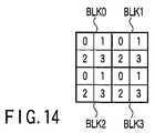
次に、この発明の第3の実施形態に係る描画装置について図13を用いて説明する。本実施形態は、上記第1、第2の実施形態において、ローカルメモリ内におけるフレームバッファに対するアドレス割り当て方法(以下、アドレッシング(addressing)と呼ぶ)に関するものである。図13は、本実施形態に係る画像描画プロセッサシステムLSI10の備えるグラフィックプロセッサ50における演算処理部54のブロック図である。画像描画プロセッサシステムLSI10の構成は、上記第1、第2の実施形態で説明した構成と同じであるが、ここでは簡単化の為に、信号処理部が4個の場合を例に挙げて説明する。 Next, a drawing apparatus according to a third embodiment of the present invention will be described with reference to FIG. The present embodiment relates to an address allocation method (hereinafter referred to as addressing) for a frame buffer in a local memory in the first and second embodiments. FIG. 13 is a block diagram of the
図示するように、演算処理部54は、ラスタライザ55及び4個の信号処理部56−0〜56−3を備えている。信号処理部56−0〜56−3のそれぞれは、ピクセル処理部PPU0〜PPU3及びローカルメモリLM0〜LM3を備えている。従って、フレームバッファは図12に示すようになる。すなわちフレームバッファは、ピクセル処理部PPU0〜PPU3で処理される(2×2)個のスタンプ群が、(2×2)個集まって形成されている。 As shown in the figure, the
なお以上の例は、説明の簡単化のために、極端に小さなフレームバッファを仮定しているものであり、実用上は、例えば(640×480)程度のフレームバッファが使用されることが通常である。 In the above example, an extremely small frame buffer is assumed for the sake of simplicity of explanation. In practice, for example, a frame buffer of about (640 × 480) is usually used. is there.
図14は、ローカルメモリLM0〜LM3のそれぞれ格納されるスタンプデータと、ローカルメモリLM0〜LM3に割り当てられるアドレスとの関係を示している。前述の通り、ローカルメモリLM0〜LM3には、ブロックBLK0〜BLK3についてのそれぞれスタンプIDがS=0、S=1、S=2、S=3のスタンプデータが格納される。従って、各ローカルメモリLM0〜LM3には、4つのスタンプデータが格納される。そして、各スタンプデータが格納されるメモリ空間のアドレスは次のようにして割り当てられている。 FIG. 14 shows a relationship between stamp data stored in the local memories LM0 to LM3 and addresses assigned to the local memories LM0 to LM3. As described above, the local memories LM0 to LM3 store stamp data with stamp IDs S = 0, S = 1, S = 2, and S = 3 for the blocks BLK0 to BLK3, respectively. Accordingly, four stamp data are stored in each of the local memories LM0 to LM3. The address of the memory space where each stamp data is stored is assigned as follows.
すなわち図15に示すように、スタンプID順ではなく、ブロックID順にアドレスが連続して割り当てられる。図15におけるアドレスは16進数で標記したものであって、1つのスタンプデータが格納されるメモリ空間は32バイトであったと仮定する。すると、まずローカルメモリLM0において、ブロックBLK0に対応するスタンプが格納されているメモリ領域の先頭アドレスに例えば“0000”が割り当てられる。先頭アドレスを“0000”としているのは説明の簡単化のためであり、特に限定されるものではない。当該メモリ領域が“0000”〜“001F”までのアドレスを占めるとすれば、次のアドレス“0020”は、ローカルメモリLM1において、ブロックBLK0に対応するスタンプが格納されているメモリ領域の先頭アドレスに割り当てられる。当該メモリ領域は“0020”〜“003F”までのアドレスを占めるから、次のアドレス“0040”は、ローカルメモリLM2において、ブロックBLK0に対応するスタンプが格納されているメモリ領域の先頭アドレスに割り当てられる。当該メモリ領域は“0040”〜“005F”までのアドレスを占めるから、次のアドレス“0060”は、ローカルメモリLM3において、ブロックBLK0に対応するスタンプが格納されているメモリ領域の先頭アドレスに割り当てられる。以上のようにして、ブロックBLK0について全てアドレスが割り当てられると、次にブロックBLK1についてアドレスが割り当てられる。以降、ブロックBLK1におけるスタンプS=0〜3についてアドレスが順次割り当てられ、その後ブロックBLK2におけるスタンプS=0〜3についてアドレスが順次割り当てられ、その後ブロックBLK3におけるスタンプS=0〜3についてアドレスが順次割り当てられる。 That is, as shown in FIG. 15, addresses are assigned consecutively in block ID order, not in stamp ID order. It is assumed that the addresses in FIG. 15 are expressed in hexadecimal numbers, and the memory space for storing one stamp data is 32 bytes. Then, first, for example, “0000” is assigned to the top address of the memory area in which the stamp corresponding to the block BLK0 is stored in the local memory LM0. The top address is set to “0000” for simplification of explanation, and is not particularly limited. If the memory area occupies addresses from “0000” to “001F”, the next address “0020” is the first address of the memory area where the stamp corresponding to the block BLK0 is stored in the local memory LM1. Assigned. Since the memory area occupies addresses from “0020” to “003F”, the next address “0040” is assigned to the start address of the memory area in which the stamp corresponding to the block BLK0 is stored in the local memory LM2. . Since the memory area occupies addresses from “0040” to “005F”, the next address “0060” is assigned to the top address of the memory area where the stamp corresponding to the block BLK0 is stored in the local memory LM3. . As described above, when all addresses are assigned to the block BLK0, next, an address is assigned to the block BLK1. Thereafter, addresses are sequentially assigned to the stamps S = 0 to 3 in the block BLK1, then addresses are sequentially assigned to the stamps S = 0 to 3 in the block BLK2, and then addresses are sequentially assigned to the stamps S = 0 to 3 in the block BLK3. It is done.
すなわち、スタンプ座標(X、Y)とブロックIDとの関係は、次に(1)式で表される。但し、スタンプ座標(X、Y)=(0、0)に相当する位置は、ブロック内の最も左上の位置であるとする。
B=X/w+(Y/h)×(fw/w) (1)
但し、BはブロックID、wはブロック1個あたりのX方向のスタンプ数、hはブロック1個あたりのY方向のスタンプ数、fwはフレームバッファ全体におけるX方向のスタンプ数である。That is, the relationship between the stamp coordinates (X, Y) and the block ID is expressed by the following equation (1). However, the position corresponding to the stamp coordinates (X, Y) = (0, 0) is assumed to be the uppermost position in the block.
B = X / w + (Y / h) × (fw / w) (1)
Where B is the block ID, w is the number of stamps in the X direction per block, h is the number of stamps in the Y direction per block, and fw is the number of stamps in the X direction in the entire frame buffer.
本実施形態で説明したアドレッシング方法によってローカルメモリへアドレスを割り付けると、スタンプ座標(X、Y)とメモリアドレスAとの関係は、下記の式(2)のようになる。
A=(B×N+S)×2d (2)
但し、スタンプのデータ幅を2dバイトとし、Nをピクセル処理部数とし、アドレスAをバイト単位のアドレスとしている。When an address is assigned to the local memory by the addressing method described in the present embodiment, the relationship between the stamp coordinates (X, Y) and the memory address A is expressed by the following equation (2).
A = (B × N + S) × 2d (2)
However, the data width of the stamp is 2d bytes, N is the number of pixel processing units, and address A is an address in bytes.
以上の結果、各ローカルメモリLM0〜LM3のメモリ空間のアドレスは図16のようになる。ローカルメモリLM0においては、ブロックBLK0に対応するデータはアドレス“0000”〜“001F”のメモリ空間に格納され、ブロックBLK1に対応するデータはアドレス“0080”〜“008F”のメモリ空間に格納され、ブロックBLK2に対応するデータはアドレス“0100”〜“011F”のメモリ空間に格納され、ブロックBLK3に対応するデータはアドレス“0180”〜“019F”のメモリ空間に格納される。 As a result, the memory space addresses of the local memories LM0 to LM3 are as shown in FIG. In the local memory LM0, data corresponding to the block BLK0 is stored in the memory space of addresses “0000” to “001F”, and data corresponding to the block BLK1 is stored in the memory space of addresses “0080” to “008F”. Data corresponding to the block BLK2 is stored in the memory space of addresses “0100” to “011F”, and data corresponding to the block BLK3 is stored in the memory space of addresses “0180” to “019F”.
ローカルメモリLM1においては、ブロックBLK0に対応するデータはアドレス“0020”〜“003F”のメモリ空間に格納され、ブロックBLK1に対応するデータはアドレス“00A0”〜“00BF”のメモリ空間に格納され、ブロックBLK2に対応するデータはアドレス“0120”〜“013F”のメモリ空間に格納され、ブロックBLK3に対応するデータはアドレス“01A0”〜“01BF”のメモリ空間に格納される。 In the local memory LM1, data corresponding to the block BLK0 is stored in the memory space of addresses “0020” to “003F”, and data corresponding to the block BLK1 is stored in the memory space of addresses “00A0” to “00BF”. Data corresponding to the block BLK2 is stored in the memory space of addresses “0120” to “013F”, and data corresponding to the block BLK3 is stored in the memory space of addresses “01A0” to “01BF”.
ローカルメモリLM2においては、ブロックBLK0に対応するデータはアドレス“0040”〜“004F”のメモリ空間に格納され、ブロックBLK1に対応するデータはアドレス“00C0”〜“00DF”のメモリ空間に格納され、ブロックBLK2に対応するデータはアドレス“0140”〜“015F”のメモリ空間に格納され、ブロックBLK3に対応するデータはアドレス“01C0”〜“01DF”のメモリ空間に格納される。 In the local memory LM2, data corresponding to the block BLK0 is stored in the memory space of addresses “0040” to “004F”, and data corresponding to the block BLK1 is stored in the memory space of addresses “00C0” to “00DF”. Data corresponding to the block BLK2 is stored in the memory space of addresses “0140” to “015F”, and data corresponding to the block BLK3 is stored in the memory space of addresses “01C0” to “01DF”.
ローカルメモリLM3においては、ブロックBLK0に対応するデータはアドレス“0060”〜“006F”のメモリ空間に格納され、ブロックBLK1に対応するデータはアドレス“00E0”〜“00FF”のメモリ空間に格納され、ブロックBLK2に対応するデータはアドレス“0160”〜“017F”のメモリ空間に格納され、ブロックBLK3に対応するデータはアドレス“01E0”〜“01FF”のメモリ空間に格納される。 In the local memory LM3, data corresponding to the block BLK0 is stored in the memory space at addresses “0060” to “006F”, and data corresponding to the block BLK1 is stored in the memory space at addresses “00E0” to “00FF”. Data corresponding to the block BLK2 is stored in the memory space of addresses “0160” to “017F”, and data corresponding to the block BLK3 is stored in the memory space of addresses “01E0” to “01FF”.
以上のように、同一ピクセル処理部によって描画されるスタンプのアドレスはとびとびの値となる。 As described above, the address of the stamp drawn by the same pixel processing unit is a discrete value.
上記のように、本実施形態に係る描画装置によれば、個々のローカルメモリ内においては、格納されるデータに割り当てられるアドレスはとびとびの値とし、ブロックID順に並べた際に連続した値となるように、アドレスを割り当てている。 As described above, according to the drawing apparatus according to the present embodiment, in each local memory, addresses assigned to stored data are discrete values, which are continuous values when arranged in block ID order. So that the address is assigned.
このようなアドレッシングを行うことで、フレームバッファのブロック数を増やした場合であっても、メモリに対するアドレス割り当てが簡便となる。例えば図14の構成においてブロックBLK4を追加した場合を考える。すると、ブロックBLK4内のスタンプS=0〜S=3のデータを保持するローカルメモリLM0〜LM3のアドレスは、ブロックBLK3、S=3の次に連続してアドレスを割り当てられればよい。 By performing such addressing, even when the number of blocks in the frame buffer is increased, it is easy to assign an address to the memory. For example, consider a case where a block BLK4 is added in the configuration of FIG. Then, the addresses of the local memories LM0 to LM3 that hold the data of the stamps S = 0 to S = 3 in the block BLK4 may be assigned consecutively after the blocks BLK3 and S = 3.
なお、本実施形態ではフレームバッファに対するアドレッシングを例に挙げて説明した。しかし、第2の実施形態に係る構成において、テクスチャデータを格納すべきローカルメモリのメモリ空間についても、同様のアドレッシングを行うことが出来る。テクスチャデータに対しても同様のアドレッシングを行うことで、例えば描画結果としてのフレームバッファを、そのままテクスチャデータとして使用することが出来る。 In the present embodiment, the addressing for the frame buffer has been described as an example. However, in the configuration according to the second embodiment, the same addressing can be performed for the memory space of the local memory where the texture data is to be stored. By performing the same addressing on the texture data, for example, a frame buffer as a rendering result can be used as it is as texture data.
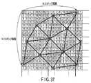
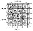
次に、この発明の第4の実施形態に係る描画装置について、図2及び図17を用いて説明する。本実施形態は、上記第1、第3の実施形態に係る構成において、フレームバッファ内におけるスタンプの配置方法に関するものである。図17は、本実施形態に係るフレームバッファの概念図である。 Next, a rendering apparatus according to a fourth embodiment of the present invention is described with reference to FIGS. The present embodiment relates to a stamp arrangement method in a frame buffer in the configurations according to the first and third embodiments. FIG. 17 is a conceptual diagram of the frame buffer according to the present embodiment.
本実施形態に係る演算処理部54は、32個のピクセル処理部56−0〜56−31を備えている。すなわち、32個のローカルメモリLM0〜LM31を備えている。従って、フレームバッファにおいて、1つのブロックが含むスタンプ数は32個である。そして、1つのブロック内のスタンプは、(8×4)のマトリクス配置されている。 The
各スタンプは、あるスタンプと、そのスタンプ周囲においてそのスタンプと同一のピクセル処理部によって描画される最近接の6個のスタンプが、ほぼ正六角形を形成するようにして配置されている。すなわち、同一ピクセル処理部で描画される近接する3個のスタンプは、ほぼ正三角形を形作る。図18は、同一ピクセル処理部によって描画されるスタンプの配置を概念的に示す。 Each stamp is arranged such that a certain stamp and the six nearest stamps drawn by the same pixel processing unit as the stamp around the stamp form a regular hexagon. That is, three adjacent stamps drawn by the same pixel processing unit form a substantially equilateral triangle. FIG. 18 conceptually shows the arrangement of stamps drawn by the same pixel processing unit.
図示するように、(6×6)個のスタンプ群を想定した際、同一ピクセル処理部に描画される3個のスタンプが、図16におけるA点、B点、及びC点に配置される。スタンプ群における左上の角部の座標を(0、0)とすれば、A点の座標は(0、6)、B点の座標は(2、0)、C点の座標は(6、4)である。そして、スタンプの縦方向(Y方向)及び横方向(X方向)の並びは、16スタンプ周期で同じ並びを繰り返す。従って、ピクセル処理部の番号S[4:0]は、スタンプのX座標の下位4ビットX[3:0]と、Y座標の下位4ビットY[3:0]とを用いて下記の(3)式で表される。
S[0]= X[0]
S[1]= Y[0]
S[2]=(X[2]xor !Y[1]and Y[2])or(X[1]and !Y[2])xor X[3]xor Y[3]
S[3]=(X[1]xor !X[2]and Y[2])or(Y[1]and !Y[2])xor X[3]xor Y[3]
S[4]= X[2]xor Y[2] (3)
但し、xorは排他的論理和演算、!は論理否定演算、orは論理和演算、andは論理積演算を示している。なお、ピクセル処理部の番号、X座標、Y座標のビットは、下位から数えたもので、スタンプ座標(X、Y)=(0、0)に相当する位置は、ブロック内の最も左上の位置であるとする。また、スタンプ座標(X、Y)とブロックIDとの関係は、上記第3の実施形態で説明した(1)式で表され、スタンプ座標(X、Y)とアドレスAとの関係は(2)式で表される。As shown in the figure, when (6 × 6) stamp groups are assumed, three stamps drawn in the same pixel processing unit are arranged at points A, B, and C in FIG. If the coordinates of the upper left corner of the stamp group are (0, 0), the coordinates of point A are (0, 6), the coordinates of point B are (2, 0), and the coordinates of point C are (6, 4). ). And the arrangement of stamps in the vertical direction (Y direction) and the horizontal direction (X direction) repeats the same arrangement with a period of 16 stamps. Accordingly, the pixel processing unit number S [4: 0] is expressed as follows using the lower 4 bits X [3: 0] of the X coordinate of the stamp and the lower 4 bits Y [3: 0] of the Y coordinate ( 3) It is expressed by the formula.
S [0] = X [0]
S [1] = Y [0]
S [2] = (X [2] xor! Y [1] and Y [2]) or (X [1] and! Y [2]) xor X [3] xor Y [3]
S [3] = (X [1] xor! X [2] and Y [2]) or (Y [1] and! Y [2]) xor X [3] xor Y [3]
S [4] = X [2] xor Y [2] (3)
However, xor represents an exclusive OR operation,! Represents a logical NOT operation, or represents a logical sum operation, and and represents a logical product operation. Note that the pixel processing unit number, the X coordinate, and the Y coordinate bit are counted from the lower order, and the position corresponding to the stamp coordinate (X, Y) = (0, 0) is the upper left position in the block. Suppose that The relationship between the stamp coordinates (X, Y) and the block ID is expressed by the equation (1) described in the third embodiment, and the relationship between the stamp coordinates (X, Y) and the address A is (2 ) Expression.
図19は、各ローカルメモリLM0〜LM31に格納されるスタンプデータと、それぞれのスタンプデータに割り付けられるアドレスとの関係を示している。図示するように、同一ピクセル処理部によって描画されるスタンプのアドレスはとびとびの値となる。 FIG. 19 shows the relationship between stamp data stored in each of the local memories LM0 to LM31 and addresses assigned to the respective stamp data. As shown in the figure, the address of the stamp drawn by the same pixel processing unit is a discrete value.
すなわち、ラスタライザ55は、投入された図形に基づいてスタンプを生成する。そして生成したスタンプを、各スタンプの座標に従って、式(3)により選択されるピクセル処理部に渡す。するとピクセル処理部は、処理結果を式(2)で求められるアドレスに格納する。 That is, the
なお、本実施形態に係るグラフィックプロセッサ50の動作は、第1の実施形態において図5を用いて説明したとおりである。但し、第1の実施形態と異なる点は、描画領域内におけるスタンプの配置が、図4のとおりでなく、図17に示す通りである点である。すなわち、ラスタライザ55が各ピクセル処理部PPU0〜PPU31へのスタンプの投入方法が異なる。本実施形態では、同一ピクセル処理部へ投入される複数のスタンプが、描画領域内において、等距離且つ等方的となる、換言すれば、各スタンプ周囲において近接する6つのスタンプが正六角形を為す。 Note that the operation of the
上記構成の描画装置によれば、第1、第3の実施形態で説明した効果が得られる。同時に、第1の実施形態に比べて、より均等に負荷が分散される。この点につき、以下詳細に説明する。 According to the drawing apparatus having the above configuration, the effects described in the first and third embodiments can be obtained. At the same time, the load is more evenly distributed than in the first embodiment. This point will be described in detail below.
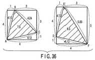
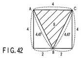
第1の実施形態における図4のようにフレームバッファを各々異なるピクセル処理部で描画されるスタンプの集合としてのブロックをマトリクス配置して形成した場合、最適なスタンプ配置は、同一ピクセル処理部により描画される最近接スタンプ同士が正三角形を形成する場合である。この場合、同一ピクセル処理部によって描画されるスタンプの隣接間隔は、いずれの方向においても最大化される。すなわち、あるスタンプの周囲の近傍スタンプは正六角形を形成し、当該スタンプから等方的な配置となる。すると、1個のスタンプは周囲に存在する6個の正三角形の頂点であるから、正三角形の個数を3倍して頂点数を数えると6回重複することになる。よって、同一ピクセル処理部に対応するスタンプ数は、正三角形の数の半分である。そして、1ブロックは2つの正三角形に覆われることになる。つまり、正三角形の面積は、ブロック面積の半分である。正三角形の一辺の長さLは、次の(4)式で表される。
√3×(L2/4)=w・h/2 (4)
従って、同一ピクセル処理部によって描画されるスタンプ同士の理想的な隣接間隔Lは、下記の(5)式で表される。
L=√(2・w・h/√3) (5)
従って、本実施形態では(3)式及び図17、図18に示すように、同一ピクセル処理部によって描画される3つの近接スタンプが、実質的な正三角形の頂点に位置するように、ピクセル処理部の割り当てを行っている。ブロックあたりに含まれるスタンプ数が(8×4)個である場合、同一ピクセル処理部に描画される近傍スタンプが形成する三角形の三辺の長さは、5.66、6.32、6.32である(図18参照)。従って、正確には正三角形ではないが、1個のブロックが(8×4)個のスタンプを含む場合において、同一ピクセル処理部で描画されるスタンプによって形成される三角形の三辺の長さを可能な限り均一にしようとすると、三辺の長さは上記のようになる。すなわち、1個のブロックが(8×4)個のスタンプを含むフレームバッファにおいて、実質的に正三角形をなしていると見ることが出来る。その結果、上記第1の実施形態と比べて、三辺の長さがより均等となり、1スタンプ周囲の6個のスタンプが実質的な正六角形を形作る。すなわち、同一ピクセル処理部によって処理されるスタンプは、互いに、実質的に等距離且つ等方的な配置となる。そのため、同一ピクセル処理部によって描画されるスタンプが、フレームバッファ上において偏りが少なくなるよう分布する。以上のように、同一ピクセル処理部に処理されるスタンプ間隔が均等になるため、どのような図形を描画する場合であっても、ピクセル処理部の負担を均等に分散させることが出来る。その結果、ピクセル処理の並列度が向上し、図形描画を高速化出来る。As shown in FIG. 4 in the first embodiment, when the frame buffer is formed by arranging blocks as a set of stamps drawn by different pixel processing units in a matrix arrangement, the optimal stamp arrangement is drawn by the same pixel processing unit. This is a case where the closest stamps form an equilateral triangle. In this case, the interval between adjacent stamps drawn by the same pixel processing unit is maximized in any direction. That is, neighboring stamps around a certain stamp form a regular hexagon and are isotropically arranged from the stamp. Then, since one stamp is the vertices of six equilateral triangles existing around it, if the number of vertices is counted by multiplying the number of equilateral triangles by three, it will overlap six times. Therefore, the number of stamps corresponding to the same pixel processing unit is half the number of equilateral triangles. One block is covered with two equilateral triangles. That is, the area of the equilateral triangle is half of the block area. The length L of one side of the equilateral triangle is expressed by the following equation (4).
√3 × (L 2/4) = w · h / 2 (4)
Therefore, an ideal adjacent interval L between stamps drawn by the same pixel processing unit is expressed by the following equation (5).
L = √ (2 · w · h / √3) (5)
Therefore, in this embodiment, as shown in the expression (3) and FIGS. 17 and 18, the pixel processing is performed so that the three proximity stamps drawn by the same pixel processing unit are located at the vertices of the substantial equilateral triangle. The division is assigned. When the number of stamps included per block is (8 × 4), the lengths of the three sides of the triangle formed by neighboring stamps drawn in the same pixel processing unit are 5.66, 6.32, 6. 32 (see FIG. 18). Therefore, although not exactly an equilateral triangle, when one block includes (8 × 4) stamps, the lengths of three sides of the triangle formed by the stamps drawn by the same pixel processing unit are set. In order to make it as uniform as possible, the length of the three sides is as described above. That is, it can be seen that one block substantially forms an equilateral triangle in a frame buffer including (8 × 4) stamps. As a result, compared to the first embodiment, the lengths of the three sides are more uniform, and the six stamps around one stamp form a substantially regular hexagon. That is, the stamps processed by the same pixel processing unit are substantially equidistant and isotropically arranged. For this reason, stamps drawn by the same pixel processing unit are distributed on the frame buffer so as to be less biased. As described above, since the stamp intervals processed by the same pixel processing unit are uniform, the burden on the pixel processing unit can be evenly distributed regardless of the type of drawing. As a result, the degree of parallelism of pixel processing is improved, and graphic drawing can be speeded up.
なお、図18に示すように、同一ピクセル処理部が処理されるスタンプによって形成される三角形の頂点座標は偶数である。従って、頂点座標の値を、X方向及びY方向ともに1/2とすることで、ブロックサイズが(4×2)スタンプ、ピクセル処理部数が8個の場合でも、第1の実施形態と同様のスタンプの配置が可能となる。この様子を示しているのが図20である。また逆に、頂点座標を整数倍しても同様の配置が可能である。図21は、頂点座標を第1の実施形態の場合の2倍にしたものであり、この場合にはブロックサイズが(16×8)スタンプ、ピクセル処理部数が128個となる。このように、ピクセル処理部数が8j2個(jは自然数)であれば、ブロックサイズを(4j×2j)スタンプ(または(2j×4j)スタンプ)として、上記第1の実施形態と同様の配置が適用できる。As shown in FIG. 18, the vertex coordinates of the triangle formed by the stamp processed by the same pixel processing unit are even numbers. Accordingly, by setting the value of the vertex coordinate to 1/2 in both the X direction and the Y direction, even when the block size is a (4 × 2) stamp and the number of pixel processing units is 8, the same as in the first embodiment Placement of stamps is possible. FIG. 20 shows this state. Conversely, the same arrangement is possible even if the vertex coordinates are multiplied by an integer. In FIG. 21, the vertex coordinates are doubled as in the first embodiment. In this case, the block size is a (16 × 8) stamp and the number of pixel processing units is 128. As described above, if the number of pixel processing units is 8j2 (j is a natural number), the block size is set to (4j × 2j) stamp (or (2j × 4j) stamp), and the same arrangement as in the first embodiment. Is applicable.
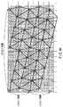
次に、この発明の第5の実施形態に係る描画装置について、図22を用いて説明する。本実施形態は、上記第2の実施形態で説明したテクセルの配置方法に、上記第4の実施形態で説明したスタンプの配置方法を適用し、更にテクスチャスタンプのアドレッシングに対して上記第3の実施形態で説明した方法を適用したものである。本実施形態に係る画像描画プロセッサシステムLSI10の備えるグラフィックプロセッサ50の構成は、第2の実施形態で説明した図8の構成と同様であるので説明は省略する。また、フレームバッファにおけるスタンプの配置、及びフレームバッファ内のスタンプのアドレッシングは、上記第4の実施形態で説明したとおりである。図22は、本実施形態に係るテクスチャの概念図である。 Next, a rendering apparatus according to a fifth embodiment of the present invention is described with reference to FIG. In this embodiment, the stamp placement method described in the fourth embodiment is applied to the texel placement method described in the second embodiment, and the third embodiment is applied to the texture stamp addressing. The method described in the embodiment is applied. Since the configuration of the
図示するように、テクスチャにおけるテクスチャブロックは、32個のテクスチャスタンプを有しており、テクスチャスタンプは(8×4)のマトリクス配置されている。 As shown in the figure, the texture block in the texture has 32 texture stamps, and the texture stamps are arranged in a matrix of (8 × 4).
各テクスチャスタンプは、第4の実施形態で説明したスタンプと同様に、各テクスチャスタンプは、あるテクスチャスタンプ周囲においてそのテクスチャスタンプと同一ローカルメモリに格納される最近接の6個のテクスチャスタンプが、ほぼ正六角形を形成するようにして配置されている。すなわち、同一ローカルメモリに格納される互いに最近接な3個のテクスチャスタンプは、ほぼ正三角形を形成する。更に換言すれば、同一ローカルメモリに格納されるテクスチャスタンプは、実質的に、互いに等距離且つ等方的に位置する。同一ローカルメモリに格納されるテクスチャスタンプの配置は、第4の実施形態で説明した図18と同様である。従って、テクスチャスタンプのX座標及びY座標と、ローカルメモリ番号LM0〜LM31との関係も(3)式で表される。 Each texture stamp is similar to the stamp described in the fourth embodiment, and each texture stamp has approximately the six nearest texture stamps stored in the same local memory around the texture stamp as the texture stamp. They are arranged so as to form a regular hexagon. That is, the three closest texture stamps stored in the same local memory form a substantially equilateral triangle. In other words, the texture stamps stored in the same local memory are located substantially equidistantly and isotropically. The arrangement of the texture stamps stored in the same local memory is the same as that in FIG. 18 described in the fourth embodiment. Therefore, the relationship between the X and Y coordinates of the texture stamp and the local memory numbers LM0 to LM31 is also expressed by equation (3).
なお、本実施形態に係るグラフィックプロセッサ50の動作は、第2の実施形態において図10を用いて説明したとおりである。但し、第2の実施形態と異なる点は、画像データ内におけるテクスチャスタンプの配置が、図9のとおりでなく、図22に示す通りである点である。すなわち、ローカルメモリLM0〜LM31へのテクスチャスタンプの記憶方法が異なる。本実施形態では、同一ローカルメモリへ投入される複数のテクスチャスタンプが、画像データ内において、等距離且つ等方的となる、換言すれば、近接する6つのテクスチャスタンプが正六角形を為す。 Note that the operation of the
本実施形態に係る描画装置によれば、上記第2、第3の実施形態で説明した効果が得られる。同時に、第2の実施形態に比べて、ローカルメモリへのアクセスをより均等に出来る。これは、第4の実施形態でスタンプについて説明したとおりである。すなわち、同一ローカルメモリに格納されるテクセルで形成される三角形の三辺の長さを可能な限り均一にしている。従って、1個のテクスチャブロックが(8×4)個のテクスチャスタンプを含むテクスチャにおいて、3個の近接テクスチャスタンプが実質的に正三角形をなしていると見ることが出来る。その結果、上記第2の実施形態と比べて、三辺の長さがより均等となり、1テクスチャスタンプ周囲の6個のテクスチャスタンプが実質的な正六角形を形作る等方的な配置となる。そのため、同一ローカルメモリに格納されるテクスチャスタンプが、テクスチャ上において偏りが少なくなるよう分布する。このように、同一ローカルメモリに格納されるテクスチャスタンプ間隔が均等になる。よって、図形の回転に依存してテクスチャデータの走査方法が変化した場合であっても、各ローカルメモリへのアクセスは均等に行われる。この点につき、以下説明する。 According to the drawing apparatus according to the present embodiment, the effects described in the second and third embodiments can be obtained. At the same time, access to the local memory can be made more even than in the second embodiment. This is as described for the stamp in the fourth embodiment. That is, the lengths of the three sides of the triangle formed by the texels stored in the same local memory are made as uniform as possible. Accordingly, in a texture in which one texture block includes (8 × 4) texture stamps, it can be seen that three adjacent texture stamps are substantially equilateral triangles. As a result, compared to the second embodiment, the lengths of the three sides are more uniform, and the six texture stamps around one texture stamp form an isotropic arrangement that forms a substantially regular hexagon. For this reason, the texture stamps stored in the same local memory are distributed so as to be less biased on the texture. In this way, the texture stamp intervals stored in the same local memory are equalized. Therefore, even when the texture data scanning method changes depending on the rotation of the figure, access to each local memory is performed equally. This will be described below.
図形を描画する場合において、スタンプの処理は例えばブロックID順に行われる。すなわち図3において、横方向に順次描画がなされていく。他方、テクスチャマッピングを行う際、ピクセルに貼り付けるべきテクセルは、必ずしもブロックID順に読み出されるとは限らない。フレームバッファ上の図形に対して、テクスチャ上のデータが回転しているような場合には、テクセルはブロックIDと全く関係なく読み出されることになる。例えば貼り付けるべきテクスチャデータが、フレームバッファ上の図形に対して90°回転していれば、フレームバッファ上では横方向に走査されるのに対して、テクスチャデータは縦方向に走査されることになる。 When drawing a graphic, stamp processing is performed in the order of block IDs, for example. That is, in FIG. 3, drawing is performed sequentially in the horizontal direction. On the other hand, when texture mapping is performed, the texels to be pasted on the pixels are not necessarily read in the order of the block IDs. When the data on the texture is rotated with respect to the graphic on the frame buffer, the texel is read out regardless of the block ID. For example, if the texture data to be pasted is rotated by 90 ° with respect to the figure on the frame buffer, the texture data is scanned in the vertical direction while the frame buffer is scanned in the horizontal direction. Become.
しかし本実施形態に係る構成であると、同一ローカルメモリに格納されるテクセルは等方的に配置されている。従って、図形の回転によってある特定のローカルメモリに格納されるテクセルに対してアクセスが集中することを回避出来る。その結果、高速なテクスチャマッピングが可能となる。 However, in the configuration according to the present embodiment, the texels stored in the same local memory are arranged isotropically. Therefore, it is possible to avoid concentration of accesses to texels stored in a specific local memory due to the rotation of the figure. As a result, high-speed texture mapping is possible.
次に、この発明の第6の実施形態に係る描画装置について説明する。本実施形態は、上記第4、第5の実施形態において、ローカルメモリ内におけるスタンプデータ及びテクセルデータの格納方法に関するものである。図23はローカルメモリのメモリ空間の概念図である。 Next, a rendering apparatus according to the sixth embodiment of the present invention is described. This embodiment relates to a method for storing stamp data and texel data in a local memory in the fourth and fifth embodiments. FIG. 23 is a conceptual diagram of the memory space of the local memory.
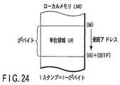
本実施形態では、図23に示すように、1つのスタンプデータは複数のデータ幅を取り得る。スタンプデータが取り得るデータ幅は、2k=1、2、4、8、…2dバイト(k、dは自然数であり、k=0〜d)である。スタンプデータが格納されるメモリ領域の開始アドレスを“0000”とすれば、スタンプデータのデータ幅が32バイト(k=5)の場合、1つのスタンプデータが占めるメモリ空間のバイト単位のアドレスは、“0000”〜“001F”である。データ幅が16バイト(k=4)の場合には“0000”〜“000F”、データ幅が8バイト(k=3)の場合には“0000”〜“0007”である。In the present embodiment, as shown in FIG. 23, one stamp data can take a plurality of data widths. The data width that the stamp data can take is 2k = 1, 2, 4, 8,... 2d bytes (k and d are natural numbers, k = 0 to d). If the start address of the memory area where the stamp data is stored is “0000”, when the data width of the stamp data is 32 bytes (k = 5), the address in bytes of the memory space occupied by one stamp data is “0000” to “001F”. When the data width is 16 bytes (k = 4), “0000” to “000F”, and when the data width is 8 bytes (k = 3), “0000” to “0007”.
そして、本実施形態では、1つのスタンプデータが取り得る最大のデータ幅に合わせて、ローカルメモリにアドレスを割り当てる。すなわち図24に示すように、1つのスタンプデータの最大データ幅が2dバイトであったとすると、各ローカルメモリは、連続したアドレスが割り当てられた2dバイトのメモリ空間を複数備える。例えばスタンプデータの最大データ幅が32バイトであったとすれば、各ローカルメモリは、32バイト単位でメモリ領域を保持し、それぞれのメモリ空間には連続したアドレスが割り当てられる。なお、以下ではこのアドレスが連続した2dバイトのメモリ領域を“単位メモリ領域UR”と便宜上呼ぶことにする。In this embodiment, an address is allocated to the local memory in accordance with the maximum data width that can be taken by one stamp data. That is, as shown in FIG. 24, if the maximum data width of one stamp data is 2d bytes, each local memory includes a plurality of 2d byte memory spaces to which consecutive addresses are assigned. For example, if the maximum data width of the stamp data is 32 bytes, each local memory holds a memory area in units of 32 bytes, and consecutive addresses are assigned to the respective memory spaces. Hereinafter, a memory area of 2d bytes in which the addresses are continuous will be referred to as a “unit memory area UR” for convenience.
次に、図24に示すようにローカルメモリにアドレスを割り当てた際の、実際のスタンプデータの格納方法について図25を用いて説明する。 Next, the actual stamp data storage method when an address is assigned to the local memory as shown in FIG. 24 will be described with reference to FIG.
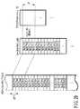
前述の通り、ローカルメモリは、2dバイトのメモリ領域(単位領域UR)毎に連続したアドレスが割り当てられている。また、1つのスタンプの最大データ幅は32バイトであると仮定する。すると、各ローカルメモリにおいて、単位領域URに割り当てられるアドレスは、(当該単位領域URの開始アドレス)〜(開始アドレス+“001F”)となる。As described above, the local memory is assigned a continuous address for each 2d- byte memory area (unit area UR). Further, it is assumed that the maximum data width of one stamp is 32 bytes. Then, in each local memory, addresses assigned to the unit area UR are (start address of the unit area UR) to (start address + “001F”).
スタンプデータ幅が、取り得る最大値の2d=32バイト(k=5)であった場合、図25に示すように、1つの単位領域URには1つのスタンプデータが格納される。これは、上記第3の実施形態で説明したとおりであり、すなわち、各ローカルメモリの単位領域URには、ブロックID順にスタンプデータが格納され、それぞれの単位領域UR内ではアドレスは連続しているが、単位領域UR間ではアドレスはとびとびの値となる。When the stamp data width is the
次に、スタンプデータのデータ幅が、2d−1=16バイト(k=4)であったとする。するとこの場合には、図25に示すように、単位領域UR内にはブロックID順に2つのスタンプデータが格納される。勿論、個々の単位領域UR内には連続したアドレスが割り当てられる。図25の例であると、ローカルメモリLM0の最初の単位領域URには、ブロックBLK0、BLK1においてピクセル処理部PPU0によって処理されるスタンプデータが格納される。そしてローカルメモリLM0における次の単位領域URには、ブロックBLK2、BLK3におけるスタンプデータが格納される。Next, it is assumed that the data width of the stamp data is 2d−1 = 16 bytes (k = 4). In this case, as shown in FIG. 25, two stamp data are stored in the unit area UR in the order of block ID. Of course, continuous addresses are assigned to each unit area UR. In the example of FIG. 25, stamp data processed by the pixel processing unit PPU0 in the blocks BLK0 and BLK1 is stored in the first unit area UR of the local memory LM0. In the next unit area UR in the local memory LM0, stamp data in the blocks BLK2 and BLK3 is stored.
次に、スタンプデータのデータ幅が、2d−2=8バイト(k=3)であったとする。すると、この場合には図25に示すように、単位領域UR内にはブロックID順に4つのスタンプデータが格納される。勿論、個々の単位領域UR内には連続したアドレスが割り当てられる。図25の例であると、ローカルメモリLM0の最初単位URには、ブロックBLK0〜BLK3においてピクセル処理部PPU0に処理されるスタンプデータが格納される。そしてローカルメモリLM0における次の単位領域URには、ブロック4〜7におけるスタンプデータが格納される。Next, it is assumed that the data width of the stamp data is 2d−2 = 8 bytes (k = 3). In this case, as shown in FIG. 25, four stamp data are stored in the unit area UR in the order of the block ID. Of course, continuous addresses are assigned to each unit area UR. In the example of FIG. 25, stamp data to be processed by the pixel processing unit PPU0 in the blocks BLK0 to BLK3 is stored in the initial unit UR of the local memory LM0. In the next unit area UR in the local memory LM0, stamp data in the
以下、スタンプデータ幅が2d−2=4バイト(k=2)の場合には、単位領域UR内には8つのスタンプデータがブロックID順に格納され、スタンプデータ幅が2d−2=2バイト(k=1)の場合には、単位領域UR内には16個のスタンプデータがブロックID順に格納され、スタンプデータ幅が2d−2=1バイト(k=0)の場合には、単位領域内には32個のスタンプデータがブロックID順に格納される。Hereinafter, when the stamp data width is 2d−2 = 4 bytes (k = 2), eight stamp data are stored in the unit area UR in the order of block ID, and the stamp data width is 2d−2 = 2. In the case of bytes (k = 1), 16 stamp data are stored in the unit area UR in the order of block ID, and when the stamp data width is 2d−2 = 1 byte (k = 0), In the unit area, 32 pieces of stamp data are stored in the order of block ID.
すなわち、スタンプについてある所定のデータ幅を基準にして、ローカルメモリへのアドレスの割り当てが行われている。そして、スタンプのデータ幅が変化したときも、ローカルメモリへのアドレスの割り当ては変化させない。その代わり、データ幅が小さい場合には、隣接ブロックから取り出した複数のスタンプデータを結合(パッキング:packing)させることにより最大値に合わせこんで、ローカルメモリへ格納している。例えばデータ幅が2d−1、すなわち最大の1/2の場合には、隣接する2つのブロックにおける同一ピクセル処理部で処理される2つのスタンプをパッキングすることにより2dバイトのデータとしてローカルメモリへ格納する。In other words, the address is assigned to the local memory based on a predetermined data width for the stamp. Even when the data width of the stamp changes, the address allocation to the local memory is not changed. Instead, when the data width is small, a plurality of stamp data extracted from adjacent blocks are combined (packed) to match the maximum value and stored in the local memory. For example, when the data width is 2d−1 , that is, the maximum of ½, two stamps processed by the same pixel processing unit in two adjacent blocks are packed to form local memory as 2d bytes of data. To store.
以上の結果、各ローカルメモリLM0〜LM31のメモリ空間のアドレスは図26のようになる。スタンプデータ幅が最大値(32バイト)の場合には、上記第3の実施形態と同様のアドレスの割り当てになる。 As a result, the addresses of the memory spaces of the local memories LM0 to LM31 are as shown in FIG. When the stamp data width is the maximum value (32 bytes), the address assignment is the same as in the third embodiment.
スタンプデータ幅が16バイトの場合には、ローカルメモリLM0においてブロックBLK0、BLK1のスタンプデータは、アドレスが連続した単位領域UR内に格納され、それぞれのアドレスは“0000”〜“000F”、“0010”〜“001F”である。ブロックBLK2、BLK3のスタンプデータは、ブロックBLK0、BLK1のスタンプデータが格納される単位領域URとはアドレスが不連続な単位領域UR内に格納され、それぞれのアドレスは“0400”〜“040F”、“0410”〜“041F”である。以下、2つのブロック毎に、アドレスが連続したそれぞれの単位領域URにスタンプデータが格納される。勿論、単位領域間のアドレスは不連続である。 When the stamp data width is 16 bytes, the stamp data of the blocks BLK0 and BLK1 is stored in the unit area UR having continuous addresses in the local memory LM0, and the addresses are “0000” to “000F” and “0010”. "-" 001F ". The stamp data of the blocks BLK2 and BLK3 are stored in the unit area UR whose addresses are discontinuous with the unit area UR in which the stamp data of the blocks BLK0 and BLK1 are stored, and each address is “0400” to “040F”, “0410” to “041F”. Hereinafter, stamp data is stored in each unit area UR having consecutive addresses for every two blocks. Of course, the addresses between the unit areas are discontinuous.
スタンプデータ幅が8バイトの場合には、ローカルメモリLM0においてブロックBLK0〜BLK3のスタンプデータは、アドレスが連続した単位領域UR内に格納され、それぞれのアドレスは“0000”〜“0007”、“0008”〜“000F”、“0010”〜“0017”、“0018”〜“001F”である。ブロックBLK4〜BLK7のスタンプデータは、ブロックBLK0〜BLK3のスタンプデータが格納される単位領域URとはアドレスが不連続な単位領域UR内に格納され、それぞれのアドレスは“0400”〜“0407”、“0408”〜“040F”、“0410”〜“0417”、“0418”〜“041F”である。以下、4つのブロック毎に、アドレスが連続したそれぞれの単位領域URにスタンプデータが格納される。勿論、単位領域間のアドレスは不連続である。 When the stamp data width is 8 bytes, the stamp data of the blocks BLK0 to BLK3 are stored in the unit area UR having continuous addresses in the local memory LM0, and the addresses are “0000” to “0007” and “0008”. ”To“ 000F ”,“ 0010 ”to“ 0017 ”, and“ 0018 ”to“ 001F ”. The stamp data of the blocks BLK4 to BLK7 are stored in the unit area UR whose addresses are discontinuous with the unit area UR in which the stamp data of the blocks BLK0 to BLK3 are stored, and each address is “0400” to “0407”, “0408” to “040F”, “0410” to “0417”, “0418” to “041F”. Hereinafter, stamp data is stored in each unit area UR having consecutive addresses for every four blocks. Of course, the addresses between the unit areas are discontinuous.
そして、上記の方法によってスタンプデータをローカルメモリへ格納した場合、各スタンプのメモリアドレスAは下記の式(6)で表される。
A=((B/2d−c)×N+S)×2d+(B mod 2d−c)×2c (6)
なお、2dはスタンプの最大データ幅であり、2d−cは、着目しているスタンプのデータ幅、modは剰余演算である。When the stamp data is stored in the local memory by the above method, the memory address A of each stamp is expressed by the following equation (6).
A = ((B / 2dc ) × N + S) × 2d + (B mod 2dc ) × 2c (6)
Incidentally, 2d is the maximum data width of the stamp, 2d-c, the data width of the stamp in question, mod is modulo operation.
すなわちラスタライザ55は、投入された図形に基づいてスタンプを生成する。そして生成したスタンプを、各スタンプの座標に従って、式(3)により選択されるピクセル処理部に渡す。するとピクセル処理部は、処理結果を式(6)で求められるアドレスに格納する。そして式(6)で求められるアドレスは、スタンプのデータ幅に依存して変化する。 That is, the
上記のように、本実施形態に係る描画装置であると、ローカルメモリに対して、スタンプデータ幅の最大値でインターリーブするアドレッシングを行っている。そして、スタンプデータ幅が最大値よりも小さい場合には、複数のスタンプをパックして最大データ幅に合わせて、ローカルメモリ内に格納し、複数のスタンプデータにつき連続したアドレスを割り当てている。その結果、アドレスはスタンプの座標だけでなく、そのデータ幅にも依存する。これは、ローカルメモリへのアドレスの割り当てを変えることなく、ローカルメモリへのスタンプの格納方法をデータ幅に合わせて変化させることを意味する。 As described above, the drawing apparatus according to the present embodiment performs addressing for interleaving with the maximum stamp data width for the local memory. If the stamp data width is smaller than the maximum value, a plurality of stamps are packed and stored in the local memory in accordance with the maximum data width, and consecutive addresses are assigned to the plurality of stamp data. As a result, the address depends not only on the stamp coordinates but also on the data width. This means that the storage method of the stamp in the local memory is changed according to the data width without changing the address assignment to the local memory.
この結果、上記第1、第3の実施形態で説明したように、ピクセル処理部の負荷を均等に分散させつつ、ピクセル処理部毎のローカルメモリに割り当てられるアドレス領域を固定したまま、複数のピクセルデータ幅に対応でき、描画処理の自由度が向上する。 As a result, as described in the first and third embodiments, while the load of the pixel processing unit is evenly distributed, the address area allocated to the local memory for each pixel processing unit is fixed and a plurality of pixels are fixed. The data width can be accommodated, and the degree of freedom of drawing processing is improved.
なお、上記実施形態ではスタンプデータをローカルメモリに格納する場合について説明したが、テクセルについても全く同様に適用できることは言うまでもない。 In the above embodiment, the case where the stamp data is stored in the local memory has been described. However, it goes without saying that the present invention can be applied to the texel in the same manner.
次に、この発明の第7の実施形態に係る描画装置について説明する。本実施形態は、上記第6の実施形態において、テクスチャユニットにテクスチャキャッシュ(texture cache)を設け、複数のテクセルデータをテクスチャキャッシュに読み出すものである。図27は、本実施形態に係る画像描画プロセッサシステムLSI10の備えるグラフィックプロセッサ50のブロック図である。 Next, a rendering apparatus according to the seventh embodiment of the present invention is described. In the sixth embodiment, a texture cache is provided in the texture unit in the sixth embodiment, and a plurality of texel data is read out to the texture cache. FIG. 27 is a block diagram of the
図示するように、本実施形態に係るグラフィックプロセッサ50は、上記第2の実施形態で説明した構成において、テクスチャユニットTUがテクスチャキャッシュTCを更に有している。テクスチャキャッシュTCは、ローカルメモリLM0〜LM31から読み出したテクスチャスタンプデータを一時的に保持する。 As illustrated, in the
本実施形態におけるフレームバッファ上のスタンプの配置は、上記第4の実施形態で説明したとおりであり、例えば図17に示すような配置である。またテクスチャスタンプの配置も、上記第5の実施形態で説明したとおりであり、例えば図22に示すような配置である。更に、ローカルメモリにおいて、テクスチャスタンプデータを格納する領域についてのアドレッシングは、上記第6の実施形態で説明した通りである。図28は、ローカルメモリのメモリ空間の概念図である。 The arrangement of the stamps on the frame buffer in this embodiment is as described in the fourth embodiment, for example, as shown in FIG. The arrangement of the texture stamp is also as described in the fifth embodiment, for example, as shown in FIG. Further, the addressing for the area storing the texture stamp data in the local memory is as described in the sixth embodiment. FIG. 28 is a conceptual diagram of the memory space of the local memory.
図示するように、ローカルメモリLM0〜LM31は、テクスチャスタンプデータの最大値である2dバイトでインターリーブされるようにアドレッシングされている。また、図28の例であると、1つのテクスチャスタンプデータのデータ幅は2d−2バイトである。従って、同一ローカルメモリに格納される4つのテクセルには、連続したアドレスが割り当てられている。As shown in the figure, the local memories LM0 to LM31 are addressed so as to be interleaved with 2d bytes which is the maximum value of the texture stamp data. In the example of FIG. 28, the data width of one texture stamp data is 2d−2 bytes. Therefore, consecutive addresses are assigned to the four texels stored in the same local memory.
上記構成において、テクスチャマッピングの際、信号処理部56−0〜56−31の読み出し回路RCは、ローカルメモリLM0〜LM31から読み出したテクスチャスタンプデータを、テクスチャキャッシュTCに格納する。図29は、一例としてローカルメモリLM0からテクスチャスタンプデータを読み出す様子を示している。 In the above configuration, at the time of texture mapping, the read circuit RC of the signal processing units 56-0 to 56-31 stores the texture stamp data read from the local memories LM0 to LM31 in the texture cache TC. FIG. 29 shows a state in which texture stamp data is read from the local memory LM0 as an example.
図示するように、読み出し回路RCは、テクスチャスタンプデータをアドレスが連続する一定サイズ単位で読み出す。例えば、テクスチャキャッシュTCに読み込まれるテクスチャスタンプデータ単位は2dバイトである。すると、テクスチャスタンプデータ幅が図28に示すように2d−2バイトであったとすると、4つのテクスチャスタンプがテクスチャキャッシュTCに読み込まれる。また、テクセルデータ幅が2d−3バイトであれば、8つのテクスチャスタンプに対して連続したアドレスが割り当てられるから、この場合には1度に8つのテクスチャスタンプがテクスチャキャッシュに読み出される。As shown in the figure, the read circuit RC reads the texture stamp data in units of a fixed size with consecutive addresses. For example, the texture stamp data unit read into the texture cache TC is 2d bytes. Then, if the texture stamp data width is 2d-2 bytes as shown in FIG. 28, four texture stamps are read into the texture cache TC. If the texel data width is 2d-3 bytes, consecutive addresses are assigned to eight texture stamps. In this case, eight texture stamps are read into the texture cache at a time.
上記構成によれば、上記第6の実施形態で説明した効果に加えて、テクスチャマッピングを効率的に行うことが出来、ピクセル処理部の負担を軽減できる。この点について、以下説明する。 According to the above configuration, in addition to the effects described in the sixth embodiment, texture mapping can be performed efficiently, and the load on the pixel processing unit can be reduced. This point will be described below.
テクスチャマッピングは、エリアシングの軽減などの観点から、ミップマッピングなどの手法により、テクセルとスタンプのサイズが1:1に近くなるように行われることが多い。この際、フレームバッファとテクスチャとに対して同じアドレッシングを行うことによって、テクスチャキャッシュのヒット率を向上させることが出来る。フレームバッファとテクスチャとが同じようにアドレッシングされていれば、テクスチャスタンプのテクスチャ上における配置は、そのローカルメモリに直結するピクセル処理部に対応したスタンプの、フレームバッファ上での位置とほぼ一致する。 From the viewpoint of reducing aliasing, texture mapping is often performed by a technique such as mip mapping so that the sizes of texels and stamps are close to 1: 1. At this time, by performing the same addressing on the frame buffer and the texture, the hit rate of the texture cache can be improved. If the frame buffer and the texture are addressed in the same manner, the arrangement of the texture stamp on the texture almost coincides with the position on the frame buffer of the stamp corresponding to the pixel processing unit directly connected to the local memory.
例えばフレームバッファが図17、テクスチャが図22のように形成されているものとする。そして、ピクセル処理部PPU0がその担当するスタンプ(S=0)を処理し、その際にローカルメモリLM21に保持されるテクスチャスタンプ(T=21)を要求したと仮定する。本実施形態では、テクスチャスタンプは1度に複数個読み出されるから、ピクセル処理部PPU0を備える信号処理部56−0のテクスチャキャッシュTUには、ローカルメモリLM21に保持される複数のテクスチャスタンプ(T=21)が格納される。すなわち、当該ピクセルに対応するテクスチャブロック以外の複数のテクスチャブロックに含まれるテクスチャスタンプも同時に読み出される。そして、ピクセル処理部PPU0が次に処理するスタンプは、最初に処理したスタンプの近傍である。 For example, it is assumed that the frame buffer is formed as shown in FIG. 17 and the texture is formed as shown in FIG. Then, it is assumed that the pixel processing unit PPU0 processes the stamp (S = 0) in charge thereof, and requests a texture stamp (T = 21) held in the local memory LM21 at that time. In the present embodiment, since a plurality of texture stamps are read at a time, the texture cache TU of the signal processing unit 56-0 including the pixel processing unit PPU0 has a plurality of texture stamps (T = 21) is stored. That is, texture stamps included in a plurality of texture blocks other than the texture block corresponding to the pixel are also read simultaneously. Then, the next stamp processed by the pixel processing unit PPU0 is in the vicinity of the stamp processed first.
すると、フレームバッファにおけるスタンプの配置と、テクスチャにおけるテクスチャスタンプの配置とはほぼ同一である。すなわち、フレームバッファにおいては、あるスタンプの周囲において、そのスタンプと同一ピクセル処理部に処理される6個の最近接スタンプが実質的に正六角形を形成する。またテクスチャにおいては、あるテクスチャスタンプの周囲において、そのテクスチャスタンプと同一ローカルメモリに格納される6個の最近接テクスチャスタンプが実質的に正六角形を形成する。両者の配置がほぼ同一であるので、テクスチャスタンプとスタンプのサイズが1:1に近いような場合には、ピクセル処理部PPU0が次に要求するテクセルも、ローカルメモリLM21に格納されている確率が高い。そしてそのテクスチャスタンプデータは、直前の処理において、信号処理部56−0のテクスチャユニットTCに読み出されている。すなわち、ピクセル処理部PPU0が次に要求するテクスチャスタンプデータが、テクスチャキャッシュTC内に保持されている(ヒットする)確率が高い。従ってその場合、ピクセル処理部PPU0はローカルメモリLM21からテクスチャスタンプを読み出す必要が無い。そのため、高速なテクスチャマッピングが可能となる。 Then, the arrangement of the stamps in the frame buffer and the arrangement of the texture stamps in the texture are almost the same. That is, in the frame buffer, around the stamp, the six closest stamps processed by the same pixel processing unit as the stamp substantially form a regular hexagon. In the texture, around the texture stamp, the six closest texture stamps stored in the same local memory as the texture stamp substantially form a regular hexagon. Since the arrangement of both is almost the same, if the texture stamp and the stamp size are close to 1: 1, the probability that the pixel processing unit PPU0 will request the next texel is also stored in the local memory LM21. high. The texture stamp data is read out to the texture unit TC of the signal processing unit 56-0 in the immediately preceding process. That is, there is a high probability that the texture stamp data requested next by the pixel processing unit PPU0 is held (hit) in the texture cache TC. Therefore, in this case, the pixel processing unit PPU0 does not need to read the texture stamp from the local memory LM21. Therefore, high-speed texture mapping becomes possible.
なお、1度のテクスチャアクセス(テクスチャスタンプデータをローカルメモリからテクスチャキャッシュに読み出すこと)でどれだけの近傍テクスチャスタンプがテクスチャキャッシュに格納されるかは、テクスチャスタンプデータ幅、テクスチャキャッシュTCが1度に取り扱うデータ幅、及びテクスチャ上におけるブロックの配置に依存する。従って、必ずしも、特定のテクスチャスタンプの6近傍テクセル、すなわち、特定のテクスチャスタンプの周囲で六角形を形成するテクスチャスタンプが全て読み出されるとは限らない。また、テクスチャスタンプ及びスタンプの配置は、完全に等方的であるわけではない。従って、当該スタンプを処理するピクセル処理部の番号(0〜31)と、当該スタンプに貼り付けるべきテクスチャスタンプを保持するローカルメモリの番号(0〜31)とが一致しない場合、スタンプの配置とテクスチャスタンプの配置とは異なることがある。更に、テクスチャは図形の回転角度に応じて回転して貼り付けられるため、スタンプの配置とテクスチャスタンプの配置とが一致していても、当該スタンプと同じ位置のテクスチャスタンプが当該スタンプに貼り付けられるわけではなく、やはり配置がずれる。しかし、本実施形態によれば、スタンプとテクスチャスタンプの配置が共に可能な限り等方的であるので、これらの配置ずれによる影響は最小限に抑えられる。 Note that how many neighboring texture stamps are stored in the texture cache by one texture access (reading the texture stamp data from the local memory to the texture cache) depends on the texture stamp data width and the texture cache TC at a time. It depends on the data width to be handled and the arrangement of blocks on the texture. Therefore, not all six neighboring texels of a specific texture stamp, that is, texture stamps that form a hexagon around the specific texture stamp are read out. Also, texture stamps and stamp placements are not completely isotropic. Therefore, if the number (0 to 31) of the pixel processing unit that processes the stamp does not match the number (0 to 31) of the local memory that holds the texture stamp to be attached to the stamp, the arrangement and texture of the stamp It may be different from the placement of the stamp. Furthermore, since the texture is rotated and pasted according to the rotation angle of the figure, even if the stamp layout matches the texture stamp layout, the texture stamp at the same position as the stamp is pasted on the stamp. Not necessarily, the arrangement is shifted. However, according to the present embodiment, since the arrangement of the stamp and the texture stamp is as isotropic as possible, the influence of these arrangement deviations can be minimized.
さらに図30に示すように、テクスチャが回転してマッピングされることで、スタンプとテクセルの配置がより近いものになりうる。図30において、フレームバッファにおける白い四角印は同一ピクセル処理部によって処理されるスタンプであり、テクスチャにおける黒い四角印はそのいずれかのスタンプを処理する際にテクスチャキャッシュに読み出されたテクスチャスタンプである。またフレームバッファにおける黒い四角印は、テクスチャキャッシュに読み出されたテクスチャスタンプが貼り付けられるスタンプの位置を示している。すなわちピクセル処理部の番号と、テクスチャスタンプを保持するローカルメモリの番号が異なることと回転角度の影響が重なっても、それぞれの効果を上回って配置がずれることはない。むしろ配置のずれは小さくなり得る。 Furthermore, as shown in FIG. 30, the texture is rotated and mapped, so that the arrangement of the stamp and the texel can be closer. In FIG. 30, a white square mark in the frame buffer is a stamp processed by the same pixel processing unit, and a black square mark in the texture is a texture stamp read to the texture cache when any one of the stamps is processed. . The black square mark in the frame buffer indicates the position of the stamp where the texture stamp read out to the texture cache is pasted. That is, even if the number of the pixel processing unit and the number of the local memory that holds the texture stamp are different from each other and the influence of the rotation angle overlaps, the arrangement does not exceed the respective effects. Rather, the misalignment can be small.
なお本実施形態において、スタンプデータ幅とテクスチャスタンプデータ幅との間には相関は無い。従って、ピクセルと異なるデータ幅のテクスチャを貼ることも可能である。そのため、上記のテクスチャキャッシュに関する記載は、フレームバッファのデータ幅に依存するものではない。 In the present embodiment, there is no correlation between the stamp data width and the texture stamp data width. Therefore, it is possible to paste a texture having a data width different from that of the pixel. Therefore, the above description regarding the texture cache does not depend on the data width of the frame buffer.
次に、この発明の第8の実施形態に係る描画装置について説明する。本実施形態は、上記第7の実施形態において、ブロックをいくつかまとめた矩形の単位(以下、スーパーブロックと呼ぶ)で配置したものである。図31は、本実施形態に係るフレームバッファの概念図である。 Next, a rendering apparatus according to the eighth embodiment of the invention is described. In this embodiment, in the seventh embodiment, the blocks are arranged in a rectangular unit (hereinafter referred to as a super block). FIG. 31 is a conceptual diagram of the frame buffer according to the present embodiment.
図示するように、スーパーブロックSBLKは、(2×4)個のブロックを含んでいる。スーパーブロックSBLKに含まれる8つのブロックのIDは、スーパーブロックSBLK内において左上から右下に向かって昇順で割り当てられている。このようなスーパーブロックSBLKが、フレームバッファ内において、水平方向に並んでいる。 As illustrated, the super block SBLK includes (2 × 4) blocks. The IDs of the eight blocks included in the super block SBLK are assigned in ascending order from the upper left to the lower right in the super block SBLK. Such super blocks SBLK are arranged in the horizontal direction in the frame buffer.
第4の実施形態で説明したとおり、スタンプの配置は、縦方向及び横方向において16スタンプ周期で同じ並びが繰り返される。従って、各々のスーパーブロックにおけるスタンプの配置は互いに同じ配置となる。そして、ブロックIDとスタンプ座標(X、Y)との関係は次の式(7)で表される。
B=(X/pw+(Y/ph)×(fw/pw))×nw×nh+(bX/w+(bY/h)×nw)
但し、
bX=X mod pw
bY=Y mod ph
nw=pw/w
nh=ph/h (7)
なる関係があり、pwはスーパーブロックのX方向のスタンプ数、phはY方向のスタンプ数である。As described in the fourth embodiment, the arrangement of stamps is repeated in the vertical direction and the horizontal direction with a period of 16 stamps. Accordingly, the stamps in each super block are arranged in the same manner. The relationship between the block ID and the stamp coordinates (X, Y) is expressed by the following equation (7).
B = (X / pw + (Y / ph) × (fw / pw)) × nw × nh + (bX / w + (bY / h) × nw)
However,
bX = X mod pw
bY = Y mod ph
nw = pw / w
nh = ph / h (7)
Where pw is the number of stamps in the X direction of the super block and ph is the number of stamps in the Y direction.
本実施形態に係る構成であると、上記第7の実施形態に比べて、よりキャッシュヒット率を向上できる。本実施形態では、同一ピクセル処理部が処理するスタンプによる六角形構造は、IDの近いブロックによって作られる。すると、式(6)から明らかなように、それらのスタンプのアドレスも近くなる。よって、このようなアドレッシングをテクスチャスタンプに適用した際に、ある特定のテクセルが読み出される際に同時にテクスチャキャッシュTCに読み出されるテクスチャスタンプには、当該テクセルの周囲に六角形を形成するものが多く含まれる。その結果、キャッシュヒット率が向上する。 With the configuration according to the present embodiment, the cache hit rate can be further improved as compared to the seventh embodiment. In this embodiment, the hexagonal structure by the stamp processed by the same pixel processing unit is created by blocks having similar IDs. Then, as is clear from equation (6), the addresses of those stamps are also close. Therefore, when such addressing is applied to a texture stamp, many of the texture stamps that are simultaneously read to the texture cache TC when a specific texel is read out form a hexagon around the texel. It is. As a result, the cache hit rate is improved.
なお、図形の境界に到達するまで走査線を変えずに水平方向に走査を続けるラスタライズ法ではなく、スーパーブロック単位で走査するラスタライズ法、すなわち、各スーパーブロックについて、その内部を順次走査する方法を用いることがより好ましい。この場合には、最初のテクセルを要求したスタンプに続いて処理されるスタンプには、直前に処理したスタンプの周囲に六角形を形成するスタンプが多く含まれる。よって、キャッシュヒット率がより向上する。 It should be noted that a rasterizing method that scans in units of super blocks, that is, a method of sequentially scanning the inside of each super block, is not a rasterizing method that continues scanning in the horizontal direction without changing the scanning line until the boundary of the figure is reached. More preferably, it is used. In this case, the stamp processed after the stamp that requested the first texel includes many stamps that form a hexagon around the stamp processed immediately before. Therefore, the cache hit rate is further improved.
なお、本実施形態ではピクセル処理部の数が32個の場合を例に挙げて説明した。従って、16スタンプ周期でスタンプの配置が繰り返されるため、スーパーブロックのサイズも(16×16)スタンプである。しかし、ピクセル処理部の数は32個に限定されるものではなく、スーパーブロックのサイズはスタンプの繰り返し周期と一致すれば良い。また、スーパーブロックのサイズとスタンプの繰り返し周期も、必ずしも一致させる必要があるわけではない。しかし、スーパーブロック内には、少なくとも1つの、同一ピクセル処理部で処理されるスタンプによる六角形が含まれることが望ましい。 In the present embodiment, the case where the number of pixel processing units is 32 has been described as an example. Accordingly, since the arrangement of the stamps is repeated at a period of 16 stamps, the size of the super block is also (16 × 16) stamps. However, the number of pixel processing units is not limited to 32, and the size of the super block only needs to match the repetition period of the stamp. Further, the size of the super block and the repetition period of the stamp do not necessarily need to be matched. However, it is desirable that at least one hexagon with a stamp processed by the same pixel processing unit is included in the super block.
次に、この発明の第9の実施形態に係る描画装置について説明する。本実施形態は、上記第4乃至第7の実施形態において、ブロック内におけるスタンプの配置を変えたものである。 Next, a rendering apparatus according to the ninth embodiment of the present invention is described. In this embodiment, the arrangement of the stamps in the block is changed in the fourth to seventh embodiments.
本実施形態に係るグラフィックプロセッサ50の演算処理部54は、図2、図8及び図27を用いて説明した構成と同様であり、ピクセル処理部数は32である。次に、フレームバッファの構成について図32を用いて説明する。 The
すなわち、図17に示す(16×16)個のスタンプの配置を、横方向に2つ並べる。そして、そのうちの一方について、縦方向に隣接するスタンプの組、すなわちX座標が同じでY=2i及びY=2i+1(iは自然数)となるスタンプ間で、処理するピクセル処理部を入れ替える。すると図示するように、第4の実施形態と同様に、あるスタンプの周囲において、そのスタンプと同一ピクセル処理部に処理される6つの最近接スタンプが、実質的な正六角形を形成する。そして、フレームバッファ内は、この実質的な正六角形によって覆われている。 That is, two (16 × 16) stamps shown in FIG. 17 are arranged in the horizontal direction. Then, for one of them, the pixel processing unit to be processed is exchanged between a pair of stamps adjacent in the vertical direction, that is, between stamps having the same X coordinate and Y = 2i and Y = 2i + 1 (i is a natural number). Then, as shown in the figure, as in the fourth embodiment, around the stamp, the six closest stamps processed by the same pixel processing unit as the stamp form a substantially regular hexagon. The frame buffer is covered with the substantial regular hexagon.
但し第4の実施形態と異なるところは、6つの最近接スタンプによって形成される六角形に含まれる三角形が、必ずしも全て同じではないということである。図17で説明した正六角形は、図33に示すように、隣接する2列のブロックに跨るようにして形成される。すなわち、フレームバッファ内は正六角形で覆われているが、2列のブロック毎に、その辺の長さが変わる。この正六角形に含まれる正三角形は、図16で説明したとおりである。しかし、三辺が(6.32、6.32、5.66)である三角形のみで形成される六角形の、横方向での隣接距離は、図33に示すように、その他の長さとなる。例えば6.40、6.08、5.39、5.00、6.71である。すなわち、図34に示すような3つの三角形が更に含まれる。すなわち、頂点座標が(0、5)、(2、0)、(6、4)であるもの、(0、6)、(2、0)、(6、5)であるもの、(0、6)、(2、0)、(6、3)であるものである。 However, the difference from the fourth embodiment is that the triangles included in the hexagon formed by the six closest stamps are not necessarily the same. As shown in FIG. 33, the regular hexagon described in FIG. 17 is formed so as to straddle two adjacent blocks. That is, the inside of the frame buffer is covered with a regular hexagon, but the length of the side changes for every two rows of blocks. The equilateral triangles included in the equilateral hexagon are as described in FIG. However, the adjacent distance in the horizontal direction of the hexagon formed only by the triangle whose three sides are (6.32, 6.32, 5.66) has other lengths as shown in FIG. . For example, 6.40, 6.08, 5.39, 5.00, and 6.71. That is, three triangles as shown in FIG. 34 are further included. That is, the vertex coordinates are (0, 5), (2, 0), (6, 4), (0, 6), (2, 0), (6, 5), (0, 6), (2, 0), (6, 3).
また、スタンプの配置は、横方向で32スタンプ、縦方向で16スタンプ周期で同じ並びが繰り返されることになる。その結果、ピクセル処理部の番号S[4:0]は、スタンプのX座標の下位5ビットX[4:0]とY座標の下位4ビットY[3:0]を用いて、下記の(8)式で表される。
S[0]= X[0]
S[1]= Y[0]xor X[4]
S[2]=(X[2]xor !Y[1]and Y[2])or(X[1]and !Y[2])xor X[3]xor Y[3]
S[3]=(X[1]xor !X[2]and Y[2])or(Y[1]and !Y[2])xor X[3]xor Y[3]
S[4]= X[2]xor Y[2] (8)
本実施形態に係る構成によれば、上記第3乃至第8の実施形態で説明した効果が得られると共に、比較的サイズの大きい図形を描画する際の処理効率を向上できる。この点について以下説明する。本実施形態に係る構成であると、上記第3乃至第8の実施形態に比べて、スタンプの横方向の繰り返し周期が大きい(32スタンプ周期)。従って、図形の境界に到達するまで走査線を変えずに水平方向に走査を続けるラスタライズ法を使用して、水平方向にサイズの大きい図形を描画する際に、ピクセル処理部にかかる負担を均等に分散できる。In addition, the same arrangement of stamps is repeated in a cycle of 32 stamps in the horizontal direction and 16 stamps in the vertical direction. As a result, the number S [4: 0] of the pixel processing unit uses the lower 5 bits X [4: 0] of the X coordinate of the stamp and the lower 4 bits Y [3: 0] of the Y coordinate as follows ( 8) It is expressed by the formula.
S [0] = X [0]
S [1] = Y [0] xor X [4]
S [2] = (X [2] xor! Y [1] and Y [2]) or (X [1] and! Y [2]) xor X [3] xor Y [3]
S [3] = (X [1] xor! X [2] and Y [2]) or (Y [1] and! Y [2]) xor X [3] xor Y [3]
S [4] = X [2] xor Y [2] (8)
According to the configuration according to the present embodiment, the effects described in the third to eighth embodiments can be obtained, and the processing efficiency when drawing a relatively large figure can be improved. This point will be described below. In the configuration according to the present embodiment, the repetition period of the stamp in the horizontal direction is larger than that in the third to eighth embodiments (32 stamp periods). Therefore, using the rasterization method that continues scanning in the horizontal direction without changing the scanning line until the boundary of the figure is reached, the burden on the pixel processing unit is evenly distributed when drawing a large figure in the horizontal direction. Can be distributed.
なお、スタンプの配置の縦と横を入れ替えれば、縦方向の繰り返し周期を大きくできる。従って、垂直方向に走査するラスタライズ法を用いて、垂直方向にサイズの大きい図形を描画する際に、負荷を均等に分散できる。 Note that if the vertical and horizontal positions of the stamps are interchanged, the repetition cycle in the vertical direction can be increased. Therefore, the load can be evenly distributed when drawing a graphic having a large size in the vertical direction by using the rasterizing method for scanning in the vertical direction.
次に、この発明の第10の実施形態に係る描画装置について、図35を用いて説明する。本実施形態は上記第4の実施形態の変形例とも言うべきもので、上記第4乃至第7の実施形態において、ブロック内におけるスタンプの配置を変えたものである。図35は、本実施形態に係るフレームバッファの概念図である。 Next, a rendering apparatus according to the tenth embodiment of the present invention is described with reference to FIG. This embodiment should be referred to as a modification of the fourth embodiment. In the fourth to seventh embodiments, the arrangement of the stamps in the block is changed. FIG. 35 is a conceptual diagram of the frame buffer according to the present embodiment.
本実施形態に係るグラフィックプロセッサ50の演算処理部54は、図2、図8及び図27を用いて説明した構成において、ピクセル処理部数を16としたものである。そして、1つのブロック内のスタンプは、(4×4)にマトリクス配置されている。 The
各スタンプは、同一のピクセル処理部によって描画される近接スタンプと共に、ほぼ正三角形を形成するように配置されている。但し、上記第4の実施形態と異なる点は、第4の実施形態では1種類の三角形が含まれるのに対し、本実施形態では2種類の三角形が含まれ、この2種類の三角形によって六角形が形成される点にある。図36は、同一ピクセル処理部によって描画されるスタンプの配置を概念的に示している。なお図36において、A〜I点は同一ピクセル処理部によって処理されるスタンプが配置される位置である。 Each stamp is arranged so as to form a substantially equilateral triangle together with a proximity stamp drawn by the same pixel processing unit. However, the fourth embodiment differs from the fourth embodiment in that the fourth embodiment includes one type of triangle, whereas the present embodiment includes two types of triangles. Is the point that is formed. FIG. 36 conceptually shows the arrangement of stamps drawn by the same pixel processing unit. In FIG. 36, points A to I are positions where stamps processed by the same pixel processing unit are arranged.
図示するように、(4×4)個のスタンプ群を想定した際、まず1つ目の三角形の頂点が、図36におけるA点、B点、及びC点に配置される。スタンプ群における左上の角部の座標を(0、0)とすれば、A点の座標は(0、4)、B点の座標は(1、0)、C点の座標は(4、3)である。次に2つ目の三角形の頂点が、図36におけるD点、E点、及びF点に配置される。D点の座標は(0、4)、E点の座標は(1、0)、F点の座標は(4、5)である。スタンプの縦方向(Y方向)及び横方向(X方向)の並びは、8スタンプ周期で同じ並びを繰り返す。従って、ピクセル処理部の番号S[3:0]は、スタンプのX座標の下位3ビットX[2:0]と、Y座標の下位3ビットY[2:0]とを用いて、下記の(9)式で表される。
S[0]=X[0]xor Y[2]
S[1]=Y[0]xor X[2]
S[2]=X[1]
S[3]=Y[1] (9)
本実施形態によれば、上記第4乃至第7の実施形態と同様の効果が得られる。本実施形態において、図36を用いて説明したA、B、C点で形成される三角形の三辺の長さは、4.24、4.12、4.12であり、D、E、F点で形成される三角形の三辺の長さは、5.83、4.12、4.12である。従って、正確には正三角形ではないが、1個のブロックが(4×4)個のスタンプを含む場合において、同一ピクセル処理部で描画されるスタンプによって形成される三角形の三辺の長さを可能な限り均一にしようとすると、三辺の長さは上記のようになる。すなわち、1個のブロックが(4×4)個のスタンプを含むフレームバッファにおいて、実質的に正三角形をなしていると見ることが出来る。その結果、上記第1の実施形態と比べて、三辺の長さがより均等となり、1スタンプ周囲の6個のスタンプが略正六角形を形作る等方的な配置となる。そのため、同一ピクセル処理部によって描画されるスタンプが、フレームバッファ上において偏りが少なくなるよう分布する。その結果、ピクセル処理部の並列度が向上し、図形描画を高速化出来る。As shown in the figure, when (4 × 4) stamp groups are assumed, first, the vertices of the first triangle are arranged at points A, B, and C in FIG. If the coordinates of the upper left corner of the stamp group are (0, 0), the coordinates of point A are (0, 4), the coordinates of point B are (1, 0), and the coordinates of point C are (4, 3). ). Next, the vertices of the second triangle are arranged at points D, E, and F in FIG. The coordinates of point D are (0, 4), the coordinates of point E are (1, 0), and the coordinates of point F are (4, 5). The arrangement of the stamps in the vertical direction (Y direction) and the horizontal direction (X direction) is repeated in a period of 8 stamps. Accordingly, the number S [3: 0] of the pixel processing unit uses the lower 3 bits X [2: 0] of the X coordinate of the stamp and the lower 3 bits Y [2: 0] of the Y coordinate as follows: It is expressed by equation (9).
S [0] = X [0] xor Y [2]
S [1] = Y [0] xor X [2]
S [2] = X [1]
S [3] = Y [1] (9)
According to the present embodiment, the same effects as those of the fourth to seventh embodiments can be obtained. In the present embodiment, the lengths of the three sides of the triangle formed by the points A, B, and C described with reference to FIG. 36 are 4.24, 4.12, and 4.12, and D, E, and F The lengths of the three sides of the triangle formed by the points are 5.83, 4.12, 4.12. Therefore, although it is not an equilateral triangle to be precise, when one block includes (4 × 4) stamps, the length of three sides of the triangle formed by the stamps drawn by the same pixel processing unit is set. In order to make it as uniform as possible, the length of the three sides is as described above. That is, it can be seen that one block substantially forms an equilateral triangle in a frame buffer including (4 × 4) stamps. As a result, compared to the first embodiment, the lengths of the three sides are more uniform, and the six stamps around one stamp form an isotropic arrangement that forms a substantially regular hexagon. For this reason, stamps drawn by the same pixel processing unit are distributed on the frame buffer so as to be less biased. As a result, the parallelism of the pixel processing units is improved, and the graphic drawing can be speeded up.
なお、本実施形態はピクセル処理部が16個の場合を例に挙げて説明したが、ピクセル処理部数が16j2個であれば、ブロックサイズを(4j×4j)スタンプとして、上記第10の実施形態と同様の配置が適用できる。The present embodiment has been described by taking a case pixel processing unit of the 16 examples, iftwo pixel processing number of copies 16j, the block size as (4j × 4j) stamp, to the tenth embodiment of the An arrangement similar to the form can be applied.
次に、この発明の第11の実施形態に係る描画装置について、図37を用いて説明する。本実施形態は上記第4の実施形態の変形例とも言うべきもので、上記第4乃至第7の実施形態において、ブロック内におけるスタンプの配置を変えたものである。図37は、本実施形態に係るフレームバッファの概念図である。 Next, a rendering apparatus according to the eleventh embodiment of the present invention is described with reference to FIG. This embodiment should be referred to as a modification of the fourth embodiment. In the fourth to seventh embodiments, the arrangement of the stamps in the block is changed. FIG. 37 is a conceptual diagram of the frame buffer according to the present embodiment.
本実施形態に係るグラフィックプロセッサ50の演算処理部54は、図2、図8及び図27を用いて説明した構成において、ピクセル処理部数を32としたものである。そして、1つのブロック内のスタンプは、(8×4)にマトリクス配置されている。 The
各スタンプは、第4の実施形態と同様に、同一のピクセル処理部によって描画される近接スタンプと共に、ほぼ正三角形を形成するように配置されている。図38は、同一ピクセル処理部によって描画されるスタンプの配置を概念的に示している。 Each stamp is arranged so as to form a substantially equilateral triangle together with a proximity stamp drawn by the same pixel processing unit, as in the fourth embodiment. FIG. 38 conceptually shows the arrangement of stamps drawn by the same pixel processing unit.
図示するように、(7×5)個のスタンプ群を想定した際、同一ピクセル処理部に描画される3個のスタンプが、図38におけるA点、B点、及びC点に配置される。スタンプ群における左上の角部の座標を(0、0)とすれば、A点の座標は(0、5)、B点の座標は(3、0)、C点の座標は(7、4)である。そして、スタンプの縦方向(Y方向)及び横方向(X方向)の並びは、16スタンプ周期で同じ並びを繰り返す。従って、ピクセル処理部の番号S[4:0]は、スタンプのX座標の下位4ビットX[3:0]と、Y座標の下位4ビットY[3:0]とを用いて、下記の(10)式で表される。
S[0]=X[2]xor !Y[0]and Y[2])or(X[0]and !Y[2])xor X[3]xor Y[3]
S[1]=X[0]xor !X[2]and Y[2])or(Y[0]and !Y[2])xor X[3]xor Y[3]
S[2]=X[1]
S[3]=Y[1]
S[4]=X[2]xor Y[2] (10)
本実施形態によれば、上記第4乃至第7の実施形態と同様の効果が得られる。本実施形態において、図38を用いて説明したA、B、C点で形成される三角形の三辺の長さは、5.66、5.83、7.07である。従って、正確には正三角形ではないが、第1の実施形態で説明した構成に比べれば、三角形の三辺の長さは均等に近づいている。そのため、同一ピクセル処理部によって描画されるスタンプが、フレームバッファ上において偏りが少なくなるよう分布する。その結果、ピクセル処理部の並列度が向上し、図形描画を高速化出来る。As shown in the figure, when (7 × 5) stamp groups are assumed, three stamps drawn in the same pixel processing unit are arranged at points A, B, and C in FIG. If the coordinates of the upper left corner of the stamp group are (0, 0), the coordinates of point A are (0, 5), the coordinates of point B are (3, 0), and the coordinates of point C are (7, 4). ). And the arrangement of stamps in the vertical direction (Y direction) and the horizontal direction (X direction) repeats the same arrangement with a period of 16 stamps. Therefore, the number S [4: 0] of the pixel processing unit uses the lower 4 bits X [3: 0] of the X coordinate of the stamp and the lower 4 bits Y [3: 0] of the Y coordinate as follows: It is represented by the formula (10).
S [0] = X [2] xor! Y [0] and Y [2]) or (X [0] and! Y [2]) xor X [3] xor Y [3]
S [1] = X [0] xor! X [2] and Y [2]) or (Y [0] and! Y [2]) xor X [3] xor Y [3]
S [2] = X [1]
S [3] = Y [1]
S [4] = X [2] xor Y [2] (10)
According to the present embodiment, the same effects as those of the fourth to seventh embodiments can be obtained. In the present embodiment, the lengths of the three sides of the triangle formed by the points A, B, and C described with reference to FIG. 38 are 5.66, 5.83, and 7.07. Therefore, although not exactly an equilateral triangle, the lengths of the three sides of the triangle are equally close compared to the configuration described in the first embodiment. For this reason, stamps drawn by the same pixel processing unit are distributed on the frame buffer so as to be less biased. As a result, the parallelism of the pixel processing units is improved, and the graphic drawing can be speeded up.
なお、本実施形態はピクセル処理部数が32の場合を例に挙げて説明したが、頂点座標を整数倍しても同様の配置が可能である。すなわち、ピクセル処理部数が32j2個であれば、ブロックサイズを(8j×4j)スタンプ(または(4j×8j)スタンプ)として、上記第11の実施形態と同様の配置が適用できる。In this embodiment, the case where the number of pixel processing units is 32 has been described as an example, but the same arrangement is possible even if the vertex coordinates are multiplied by an integer. That is, if thetwo pixel processing number of copies 32j, the block size as (8j × 4j) stamp (or (4j × 8j) stamp), the eleventh same arrangement as the embodiment of the can be applied.
次に、この発明の第12の実施形態に係る描画装置について、図39を用いて説明する。本実施形態は上記第4の実施形態の変形例とも言うべきもので、上記第4乃至第7の実施形態において、ブロック内におけるスタンプの配置を変えたものである。図39は、本実施形態に係るフレームバッファの概念図である。 Next, a rendering apparatus according to the twelfth embodiment of the present invention is described with reference to FIG. This embodiment should be referred to as a modification of the fourth embodiment. In the fourth to seventh embodiments, the arrangement of the stamps in the block is changed. FIG. 39 is a conceptual diagram of the frame buffer according to the present embodiment.
本実施形態に係るグラフィックプロセッサ50の演算処理部54は、図2、図8及び図27を用いて説明した構成において、ピクセル処理部数を32としたものである。そして、1つのブロック内のスタンプは、(8×4)にマトリクス配置されている。 The
各スタンプは、第4の実施形態と同様に、同一のピクセル処理部によって描画される近接スタンプと共に、三角形を形成するように配置されている。また、近傍の4つのスタンプは、正方形を形成する。図40は、同一ピクセル処理部によって描画されるスタンプの配置を概念的に示している。 Each stamp is arranged so as to form a triangle together with the proximity stamp drawn by the same pixel processing unit, as in the fourth embodiment. Also, the four nearby stamps form a square. FIG. 40 conceptually shows the arrangement of stamps drawn by the same pixel processing unit.
図示するように、(8×4)個のスタンプ群を想定した際、同一ピクセル処理部に描画される3個のスタンプが、図38におけるA点、B点、及びC点に配置される。スタンプ群における左上の角部の座標を(0、0)とすれば、A点の座標は(0、0)、B点の座標は(4、4)、C点の座標は(8、0)である。そして、スタンプの縦方向(Y方向)及び横方向(X方向)の並びは、8スタンプ周期で同じ並びを繰り返す。従って、ピクセル処理部の番号S[4:0]は、スタンプのX座標の下位4ビットX[2:0]、Y座標の下位3ビットY[2:0]とを用いて、下記の(11)式で表される。
S[0]=X[0]
S[1]=Y[0]
S[2]=X[1]
S[3]=Y[1]
S[4]=X[2]xorY[2] (11)
本実施形態によれば、上記第4乃至第7の実施形態と同様の効果が得られる。本実施形態において、図40を用いて説明したA、B、C点で形成される三角形の三辺の長さは、8、5.66、5.66である。従って、正三角形ではないが、第1の実施形態で説明した構成に比べれば、三角形の三辺の長さは均等に近づいている。そのため、同一ピクセル処理部によって描画されるスタンプが、フレームバッファ上において偏りが少なくなるよう分布する。その結果、ピクセル処理部の並列度が向上し、図形描画を高速化出来る。As shown in the figure, when (8 × 4) stamp groups are assumed, three stamps drawn in the same pixel processing unit are arranged at points A, B, and C in FIG. If the coordinates of the upper left corner of the stamp group are (0, 0), the coordinates of point A are (0, 0), the coordinates of point B are (4, 4), and the coordinates of point C are (8, 0). ). And the arrangement of stamps in the vertical direction (Y direction) and the horizontal direction (X direction) is repeated in a period of 8 stamps. Accordingly, the number S [4: 0] of the pixel processing unit uses the lower 4 bits X [2: 0] of the X coordinate of the stamp and the lower 3 bits Y [2: 0] of the Y coordinate as follows ( 11)
S [0] = X [0]
S [1] = Y [0]
S [2] = X [1]
S [3] = Y [1]
S [4] = X [2] xorY [2] (11)
According to the present embodiment, the same effects as those of the fourth to seventh embodiments can be obtained. In the present embodiment, the lengths of the three sides of the triangle formed by the points A, B, and C described with reference to FIG. 40 are 8, 5.66, and 5.66. Therefore, although it is not an equilateral triangle, the lengths of the three sides of the triangle are evenly approached compared to the configuration described in the first embodiment. For this reason, stamps drawn by the same pixel processing unit are distributed on the frame buffer so as to be less biased. As a result, the parallelism of the pixel processing units is improved, and the graphic drawing can be speeded up.
また、スタンプの繰り返し周期は第4の実施形態に比べて短く、ピクセル処理部の番号S[4:0]の計算式も第4の実施形態の場合に比べて単純である。従って、この計算に必要な回路のコストを低減できる。 Also, the stamp repetition cycle is shorter than that of the fourth embodiment, and the calculation formula of the pixel processing unit number S [4: 0] is simpler than that of the fourth embodiment. Therefore, the cost of the circuit required for this calculation can be reduced.
なお、図40に示すように、同一ピクセル処理部が処理されるスタンプによって形成される三角形の頂点座標は全て4の倍数である。従って、頂点座標の値を、X方向及びY方向ともに1/2、または1/4とすることで、ブロックサイズが(4×2)スタンプ、ピクセル処理部数が8個の場合、及び(2×1)スタンプ、ピクセル処理部数が2個の場合でも、同様のスタンプの配置が可能となる。このように、ピクセル処理部数が2j2個(jは自然数)であれば、ブロックサイズを(2j×j)スタンプ(または(j×2j)スタンプ)として、上記第12の実施形態と同様の配置が適用できる。As shown in FIG. 40, the vertex coordinates of the triangle formed by the stamp processed by the same pixel processing unit are all multiples of 4. Therefore, by setting the value of the vertex coordinates to 1/2 or 1/4 in both the X direction and the Y direction, the block size is (4 × 2) stamp, the number of pixel processing copies is 8, and (2 × 1) Even when the number of stamp and pixel processing units is two, the same stamp arrangement is possible. Thus, if the number of pixel processing units is 2j2 (j is a natural number), the block size is set to (2j × j) stamp (or (j × 2j) stamp), and the same arrangement as in the twelfth embodiment. Is applicable.
次に、この発明の第13の実施形態に係る描画装置について、図41を用いて説明する。本実施形態は上記第4の実施形態の変形例とも言うべきもので、上記第4乃至第7の実施形態において、ブロック内におけるスタンプの配置を変えたものである。図41は、本実施形態に係るフレームバッファの概念図である。 Next, a rendering apparatus according to the thirteenth embodiment of the present invention is described with reference to FIG. This embodiment should be referred to as a modification of the fourth embodiment. In the fourth to seventh embodiments, the arrangement of the stamps in the block is changed. FIG. 41 is a conceptual diagram of the frame buffer according to the present embodiment.
本実施形態に係るグラフィックプロセッサ50の演算処理部54は、図2、図8及び図27を用いて説明した構成において、ピクセル処理部数を16としたものである。そして、1つのブロック内のスタンプは、(4×4)にマトリクス配置されている。 The
各スタンプは、そのスタンプの周囲の同一のピクセル処理部によって描画される6個のスタンプがほぼ正六角形を形成するようにして配置されている。すなわち、同一ピクセル処理部で描画される互いに最近接な3個のスタンプは、正三角形に近い配置をとる。図42は、同一ピクセル処理部によって描画されるスタンプの配置を概念的に示す。 Each stamp is arranged so that six stamps drawn by the same pixel processing unit around the stamp form a substantially regular hexagon. That is, the three closest stamps drawn by the same pixel processing unit are arranged close to an equilateral triangle. FIG. 42 conceptually shows the arrangement of stamps drawn by the same pixel processing unit.
図示するように、(4×4)個のスタンプ群を想定した際、同一ピクセル処理部に描画される3個のスタンプが、図40におけるA点、B点、及びC点に配置される。スタンプ群における左上の角部の座標を(0、0)とすれば、A点の座標は(0、0)、B点の座標は(2、4)、C点の座標は(4、0)である。そして、スタンプの縦方向(Y方向)及び横方向(X方向)の並びは、それぞれ4スタンプ、8スタンプ周期で同じ並びを繰り返す。従って、ピクセル処理部の番号S[3:0]は、スタンプのX座標の下位2ビットX[1:0]と、Y座標の下位3ビットY[2:0]とを用いて、下記の(12)式で表される。
S[0]=X[0]
S[1]=Y[0]
S[2]=X[1]xorY[2]
S[3]=Y[1] (12)
本実施形態によれば、上記第4乃至第7の実施形態と同様の効果が得られる。本実施形態において、図42を用いて説明したA、B、C点で形成される三角形の三辺の長さは、4、4.47、4.47である。従って、正確には正三角形ではないが、第1の実施形態で説明した構成に比べれば、三角形の三辺の長さは均等に近づいている。その結果、1スタンプ周囲の6個のスタンプが実質的な正六角形を形作る等方的な配置となる。そのため、同一ピクセル処理部によって描画されるスタンプが、フレームバッファ上において偏りが少なくなるよう分布する。その結果、ピクセル処理部の並列度が向上し、図形描画を高速化出来る。As shown in the drawing, when (4 × 4) stamp groups are assumed, three stamps drawn in the same pixel processing unit are arranged at points A, B, and C in FIG. If the coordinates of the upper left corner of the stamp group are (0, 0), the coordinates of point A are (0, 0), the coordinates of point B are (2, 4), and the coordinates of point C are (4, 0). ). The stamps in the vertical direction (Y direction) and the horizontal direction (X direction) are repeated in a cycle of 4 stamps and 8 stamps, respectively. Therefore, the number S [3: 0] of the pixel processing unit uses the lower 2 bits X [1: 0] of the X coordinate of the stamp and the lower 3 bits Y [2: 0] of the Y coordinate as follows: It is expressed by equation (12).
S [0] = X [0]
S [1] = Y [0]
S [2] = X [1] xorY [2]
S [3] = Y [1] (12)
According to the present embodiment, the same effects as those of the fourth to seventh embodiments can be obtained. In the present embodiment, the lengths of the three sides of the triangle formed by the points A, B, and C described with reference to FIG. 42 are 4, 4.47, and 4.47. Therefore, although not exactly an equilateral triangle, the lengths of the three sides of the triangle are equally close compared to the configuration described in the first embodiment. As a result, the six stamps around one stamp form an isotropic arrangement that forms a substantially regular hexagon. For this reason, stamps drawn by the same pixel processing unit are distributed on the frame buffer so as to be less biased. As a result, the parallelism of the pixel processing units is improved, and the graphic drawing can be speeded up.
なお、図42に示すように、同一ピクセル処理部が処理されるスタンプによって形成される三角形の頂点座標は全て偶数である。従って、頂点座標の値を、X方向及びY方向ともに1/2、またはとすることで、ブロックサイズが(2×2)スタンプ、ピクセル処理部数が4個の場合でも、同様のスタンプの配置が可能となる。このように、ピクセル処理部数が4j2個であれば、ブロックサイズを(2j×2j)スタンプとして、上記第13の実施形態と同様の配置が適用できる。As shown in FIG. 42, the vertex coordinates of the triangle formed by the stamp processed by the same pixel processing unit are all even numbers. Therefore, by setting the vertex coordinate value to 1/2 or both in the X direction and the Y direction, even when the block size is a (2 × 2) stamp and the number of pixel processing units is 4, the same stamp arrangement can be achieved. It becomes possible. Thus, iftwo pixel processing number of copies 4j, the block size as (2j × 2j) stamp, the thirteenth same arrangement as the embodiment of the can be applied.
次に、この発明の第14の実施形態に係る描画装置について、図43を用いて説明する。本実施形態は上記第9の実施形態の変形例とも言うべきもので、上記第4乃至第9の実施形態において、ブロック内におけるスタンプの配置を変えたものである。図43は、本実施形態に係るフレームバッファの概念図である。 Next, a rendering apparatus according to the fourteenth embodiment of the present invention is described with reference to FIG. This embodiment should be referred to as a modification of the ninth embodiment. In the fourth to ninth embodiments, the arrangement of the stamps in the block is changed. FIG. 43 is a conceptual diagram of the frame buffer according to the present embodiment.
本実施形態に係るグラフィックプロセッサ50の演算処理部54は、図2、図8及び図27を用いて説明した構成において、ピクセル処理部数を16としたものである。そして、1つのブロック内のスタンプは、(4×4)にマトリクス配置されている。そして、フレームバッファは次のようにして形成されている。 The
すなわち、図33で示した(8×8)個のスタンプの配置を、横方向に2つ並べる。そして、そのうちの一方について、縦方向に1スタンプおきの組、すなわちX座標が同じでY=4i及びY=4i+2(iは自然数)となるスタンプ間と、X座標が同じでY=4i+1及びY=4i+3となるスタンプ間で、処理するピクセル処理部を入れ替える。すると、図示するように、隣接する2行のブロックに跨るようにして、図36で説明したA、B、C点で形成される三角形、すなわち実質的な正三角形が形作られる。スタンプの配置は、横方向で16スタンプ、縦方向で8スタンプ周期の繰り返しとなる。その結果、ピクセル処理部の番号S[3:0]は、スタンプのX座標の下位4ビットX[3:0]と、Y座標の下位3ビットY[2:0]とを用いて、下記の(13)式で表される。
S[0]=X[0]xor Y[2]
S[1]=Y[0]xor X[2]
S[2]=X[1]
S[3]=Y[1]xor X[3] (13)
本実施形態に係る構成によれば、上記第3乃至第7の実施形態で説明した効果が得られると共に、比較的サイズの大きい図形を描画する際の処理効率を向上できる。この点について以下説明する。本実施形態に係る構成であると、上記第3乃至第7の実施形態に比べて、スタンプの横方向の繰り返し周期が大きい(16スタンプ周期)。従って、図形の境界に到達するまで走査線を変えずに水平方向に走査を続けるラスタライズ法を使用して、水平方向にサイズの大きい図形を描画する際に、ピクセル処理部にかかる負担を均等に分散できる。但し本実施形態であると、三角形の頂点の一つが(3、1)となり、長さ3.16という、他より辺の短い三角形が含まれる。That is, two (8 × 8) stamps shown in FIG. 33 are arranged in the horizontal direction. For one of them, every other pair of stamps in the vertical direction, that is, between stamps where the X coordinate is the same and Y = 4i and Y = 4i + 2 (i is a natural number), and the X coordinate is the same, Y = 4i + 1 and Y The pixel processing unit to be processed is exchanged between stamps of = 4i + 3. Then, as shown in the figure, a triangle formed by the points A, B, and C described in FIG. 36, that is, a substantial equilateral triangle is formed so as to straddle two adjacent rows of blocks. The stamp arrangement is 16 stamps in the horizontal direction and 8 stamps in the vertical direction. As a result, the pixel processing unit number S [3: 0] uses the lower 4 bits X [3: 0] of the X coordinate of the stamp and the lower 3 bits Y [2: 0] of the Y coordinate as follows: (13).
S [0] = X [0] xor Y [2]
S [1] = Y [0] xor X [2]
S [2] = X [1]
S [3] = Y [1] xor X [3] (13)
According to the configuration of the present embodiment, the effects described in the third to seventh embodiments can be obtained, and the processing efficiency when drawing a relatively large figure can be improved. This point will be described below. In the configuration according to the present embodiment, the repetition cycle of the stamp in the horizontal direction is larger than that in the third to seventh embodiments (16 stamp cycles). Therefore, using the rasterization method that continues scanning in the horizontal direction without changing the scanning line until the boundary of the figure is reached, the burden on the pixel processing unit is evenly distributed when drawing a large figure in the horizontal direction. Can be distributed. However, in the present embodiment, one of the vertices of the triangle is (3, 1), and a triangle having a length of 3.16 and a shorter side than the other is included.
なお、スタンプの配置の縦と横を入れ替えれば、縦方向の繰り返し周期を大きくできる。従って、垂直方向に走査するラスタライズ法を用いて、垂直方向にサイズの大きいの図形を描画する際に、負荷を均等に分散できる。 Note that if the vertical and horizontal positions of the stamps are interchanged, the repetition cycle in the vertical direction can be increased. Accordingly, the load can be evenly distributed when a large-sized figure is drawn in the vertical direction by using the rasterizing method for scanning in the vertical direction.
次に、この発明の第15の実施形態に係る描画装置について、図44を用いて説明する。本実施形態は上記第9の実施形態の変形例とも言うべきもので、上記第4乃至第9の実施形態において、ブロック内におけるスタンプの配置を変えたものである。図44は、本実施形態に係るフレームバッファの概念図である。 Next, a rendering apparatus according to the fifteenth embodiment of the present invention is described with reference to FIG. This embodiment should be referred to as a modification of the ninth embodiment. In the fourth to ninth embodiments, the arrangement of the stamps in the block is changed. FIG. 44 is a conceptual diagram of a frame buffer according to the present embodiment.
本実施形態に係るグラフィックプロセッサ50の演算処理部54は、図2、図8及び図27を用いて説明した構成において、ピクセル処理部数を16としたものである。そして、1つのブロック内のスタンプは、(4×4)にマトリクス配置されている。そして、フレームバッファは次のようにして形成されている。 The
すなわち、図43で示した構成において、横方向の周期を32スタンプとする。すると、図示するように、図36で説明したA、B、C点で形成される三角形、すなわち実質的な正三角形が形作られる。スタンプの配置は、横方向で32スタンプ、縦方向で8スタンプ周期の繰り返しとなる。その結果、ピクセル処理部の番号S[3:0]は、スタンプのX座標の下位5ビットX[4:0]と、Y座標の下位3ビットY[2:0]とを用いて、下記の(14)式で表される。
S[0]=(!X[0]xor X[2]xor Y[0]xor Y[1]and X[3])or(X[0]and !X[3])xor X[4]xor Y[2]
S[1]=Y[0]xor X[2]
S[2]=X[1]
S[3]=Y[1]xor X[3] (14)
本実施形態に係る構成によれば、上記第3乃至第7の実施形態で説明した効果が得られる。また第14の実施形態と同様に、比較的サイズの大きい図形を描画する際の処理効率を向上できる。また、第9、第14の実施形態のようにフレームバッファを覆う三角形のうちで、他より辺の短い三角形が含まれることがない。換言すれば、フレームバッファ内は第10の実施形態で述べた、実質的な正三角形と言うことの出来る図36で説明した2種類の三角形によって覆われている。本実施形態は、スタンプの繰り返し周期を長くすることによって、第14の実施形態において存在したスタンプ間距離が小さくなる部分を解消したものである。That is, in the configuration shown in FIG. 43, the horizontal period is 32 stamps. Then, as shown in the figure, a triangle formed by the points A, B, and C described in FIG. 36, that is, a substantial equilateral triangle is formed. The arrangement of the stamps is 32 stamps in the horizontal direction and 8 stamps in the vertical direction. As a result, the pixel processing unit number S [3: 0] uses the lower 5 bits X [4: 0] of the X coordinate of the stamp and the lower 3 bits Y [2: 0] of the Y coordinate as follows: (14).
S [0] = (! X [0] xor X [2] xor Y [0] xor Y [1] and X [3]) or (X [0] and! X [3]) xor X [4] xor Y [2]
S [1] = Y [0] xor X [2]
S [2] = X [1]
S [3] = Y [1] xor X [3] (14)
According to the configuration according to the present embodiment, the effects described in the third to seventh embodiments can be obtained. Further, as in the fourteenth embodiment, the processing efficiency when drawing a relatively large figure can be improved. Further, among the triangles covering the frame buffer as in the ninth and fourteenth embodiments, triangles with shorter sides than the others are not included. In other words, the frame buffer is covered with the two types of triangles described in FIG. 36 and described in FIG. 36, which can be regarded as substantial equilateral triangles. In the present embodiment, the portion where the distance between stamps is reduced in the fourteenth embodiment is eliminated by increasing the stamp repetition period.
勿論、スタンプの配置の縦と横を入れ替えれば、垂直方向にサイズの大きいの図形を描画する際に、負荷を均等に分散できる。 Of course, if the vertical and horizontal positions of the stamps are interchanged, the load can be evenly distributed when drawing a large graphic in the vertical direction.
上記のように、この発明の第1乃至第15の実施形態によれば、フレームバッファを複数のブロックによって形成している。各々のブロックには、ピクセル処理部の数に等しい数のスタンプが設けられ、各ブロック内においては、それぞれのスタンプは異なるピクセル処理部で処理される。このようなスタンプ配置を採用することで、ピクセル処理部の負担を均等に分散出来る。更にこのようなスタンプ配置は、テクスチャにも適用出来る。テクスチャに適用した際には、ローカルメモリへのアクセスを均等に分散出来る。以上の結果、図形の描画速度を向上できる。また、ローカルメモリのアドレスは、各ローカルメモリ毎に連続した値が割り当てられるのではなく、異なるメモリ間で、同一のブロックに所属するスタンプ順に連続して割り当てられている。従って、ブロック数を増加させる場合のアドレスの割り当て方が簡便となり、描画装置の負担を軽減できる。 As described above, according to the first to fifteenth embodiments of the present invention, the frame buffer is formed of a plurality of blocks. Each block is provided with a number of stamps equal to the number of pixel processing units, and within each block, each stamp is processed by a different pixel processing unit. By adopting such a stamp arrangement, the load on the pixel processing unit can be evenly distributed. Furthermore, such a stamp arrangement can also be applied to texture. When applied to textures, access to local memory can be evenly distributed. As a result, the drawing speed of graphics can be improved. The local memory addresses are not assigned consecutive values for each local memory, but are successively assigned between different memories in the order of stamps belonging to the same block. Therefore, the method of assigning addresses when the number of blocks is increased is simplified, and the burden on the drawing apparatus can be reduced.
そして、例えば第4、第5の実施形態では、ブロック及びテクスチャブロックは(8×4)個のスタンプ及びテクスチャスタンプを含んでいる。そして、各スタンプ(テクスチャスタンプ)は、同一ピクセル処理部で処理される(同一ローカルメモリに格納される)3つのスタンプ(テクセル)が、実質的に正三角形の頂点に位置するように配置されている。更に第4、第5の実施形態では、フレームバッファ内において、前記三角形が隙間無く配列されている。従って、あるスタンプ周囲の6個の近傍スタンプは、当該スタンプを中心とした、実質的な正六角形の頂点に位置する。従って、同一ピクセル処理部によって処理されるスタンプは、フレームバッファ内において偏り無く均一に分布する。すなわち、同一ピクセル処理部によって処理されるスタンプは、実質的に、互いに等距離且つ等方的に位置する。また、フレームバッファとテクスチャとを同じアドレッシング方法でローカルメモリに格納しているため、描画結果としてのフレームバッファを、そのままテクスチャとして以降の描画処理に使用することが出来る。 For example, in the fourth and fifth embodiments, the block and the texture block include (8 × 4) stamps and texture stamps. Each stamp (texture stamp) is arranged so that three stamps (texels) processed by the same pixel processing unit (stored in the same local memory) are substantially located at the vertices of an equilateral triangle. Yes. Furthermore, in the fourth and fifth embodiments, the triangles are arranged without a gap in the frame buffer. Accordingly, six neighboring stamps around a certain stamp are located at the vertices of a substantially regular hexagon centering on the stamp. Therefore, stamps processed by the same pixel processing unit are uniformly distributed in the frame buffer. That is, the stamps processed by the same pixel processing unit are substantially equidistant and isotropic. Further, since the frame buffer and the texture are stored in the local memory by the same addressing method, the frame buffer as a drawing result can be used as it is for the subsequent drawing processing as the texture.
また、スタンプ座標からピクセル処理部の番号を計算するには、座標データのビットを取り出して論理演算を行うのみで良い。従って、計算が簡単であり、そのための回路規模を縮小出来る。 Further, in order to calculate the pixel processing unit number from the stamp coordinates, it is only necessary to extract the bits of the coordinate data and perform a logical operation. Therefore, the calculation is simple and the circuit scale for the calculation can be reduced.
また第6の実施形態では更に、ローカルメモリに対して、スタンプデータの最大値でインターリーブするようなアドレッシングを行っている。そして、スタンプデータのデータ幅が最大値より小さい場合には、複数のスタンプデータをパックしてローカルメモリに格納している。従って、ローカルメモリに対するアドレスの割り当てを変えることなく、複数のデータ幅のスタンプに対応することが出来、描画処理の自由度が向上する。 In the sixth embodiment, the local memory is further addressed so as to interleave with the maximum value of the stamp data. If the data width of the stamp data is smaller than the maximum value, a plurality of stamp data is packed and stored in the local memory. Therefore, it is possible to deal with a plurality of data width stamps without changing the address assignment to the local memory, and the degree of freedom of the drawing process is improved.
更に第7の実施形態では更に、テクスチャユニットにキャッシュメモリを設けている。そして、テクスチャマッピングの際に、1度に複数のテクセルをテクスチャキャッシュに読み出している。この際、フレームバッファとテクスチャとに対して、同じアドレッシングを行うことで、テクスチャキャッシュのヒット率を向上できる。 Furthermore, in the seventh embodiment, a cache memory is provided in the texture unit. At the time of texture mapping, a plurality of texels are read into the texture cache at a time. At this time, by performing the same addressing on the frame buffer and the texture, the texture cache hit rate can be improved.
更に、スタンプの配置方法は、第8乃至第15の実施形態で説明した配置にすることも可能である。第8、第9、第14、第15の実施形態に係る配置方法であると、同一ピクセル処理部に対応するスタンプの、水平方向の繰り返し周期を大きくしている。従って、図形の境界に到達するまで走査線を変えずに水平に走査し続けるラスタライズ法を使用して大きい図形を描画する際の処理効率を向上できる。なお、第8乃至第15の実施形態では、スタンプの配置の例を挙げて説明したが、テクスチャスタンプについても同様の配置を適用できることは言うまでもない。 Furthermore, the stamp arrangement method can be the arrangement described in the eighth to fifteenth embodiments. In the arrangement methods according to the eighth, ninth, fourteenth and fifteenth embodiments, the horizontal repetition period of the stamp corresponding to the same pixel processing unit is increased. Therefore, it is possible to improve the processing efficiency when drawing a large figure by using a rasterizing method that continues to scan horizontally without changing the scanning line until the figure boundary is reached. In the eighth to fifteenth embodiments, examples of stamp arrangement have been described. Needless to say, the same arrangement can be applied to texture stamps.
また、上記実施形態で説明したブロックは、縦と横とを入れ替えることも出来る。例えば、スタンプ及びテクセルが(8×4)個にマトリクス配置されているものについては、縦と横を入れ替えて、(4×8)個にマトリクス配置されている場合でも適用可能である。 Further, the blocks described in the above embodiments can be interchanged vertically and horizontally. For example, in the case where (8 × 4) stamps and texels are arranged in a matrix, the present invention can be applied even when the matrix is arranged in (4 × 8) by replacing the vertical and horizontal.
また、上記実施形態では1個のスタンプが(4×4)個のピクセルを含む場合について説明した。しかし、スタンプに含まれるピクセルの数は特に限定されるものではない。例えば1個のスタンプに含まれるピクセルの数は1個であっても勿論良い。その場合には、上記実施形態における「スタンプ」を「ピクセル」と読み替えれば、そのまま適用できる。このことは、テクセルについても同様であり、「テクスチャスタンプ」を「テクセル」と読み替えても良い。但し、テクスチャスタンプ内に含まれるテクセル数は、スタンプ内に含まれるピクセル数と同じにすることが望ましい。 In the embodiment described above, the case where one stamp includes (4 × 4) pixels has been described. However, the number of pixels included in the stamp is not particularly limited. For example, the number of pixels included in one stamp may be one. In that case, if “stamp” in the above embodiment is read as “pixel”, it can be applied as it is. The same applies to texels, and “texture stamp” may be read as “texel”. However, the number of texels included in the texture stamp is desirably the same as the number of pixels included in the stamp.
なお、上記第1乃至第15の実施形態に係る画像処理装置は、例えばゲーム機、ホームサーバー、テレビ、または携帯情報端末などに搭載することが出来る。図45は上記第1乃至第15の実施形態に係る画像処理装置を備えたデジタルテレビの備えるデジタルボードのブロック図である。デジタルボードは、画像・音声などの通信情報を制御するためのものである。図示するように、デジタルボード100は、フロントエンド部110、画像描画プロセッサシステム120、デジタル入力部130、A/Dコンバータ140、180、ゴーストリダクション部150、三次元YC分離部160、カラーデコーダ170、LAN処理LSI190、LAN端子200、ブリッジメディアコントローラ210、カードスロット220、フラッシュメモリ230、及び大容量メモリ(例えばDRAM:Dynamic Random Access Memory)240を備えている。フロントエンド部110は、デジタルチューナーモジュール111、112、OFDM(Orthogonal Frequency Division Multiplex)復調部113、QPSK(Quadrature Phase Shift Keying)復調部114を備えている。 The image processing apparatus according to the first to fifteenth embodiments can be mounted on, for example, a game machine, a home server, a television, or a portable information terminal. FIG. 45 is a block diagram of a digital board provided in a digital television provided with the image processing apparatus according to the first to fifteenth embodiments. The digital board is for controlling communication information such as images and sounds. As illustrated, the
画像描画プロセッサシステム120は、送受信回路121、MPEG2デコーダ122、グラフィックエンジン123、デジタルフォーマットコンバータ124、及びプロセッサ125を備えている。そして、例えばグラフィックエンジン123及びプロセッサ125が、上記第1乃至第15の実施形態で説明したグラフィックプロセッサ50及びホストプロセッサ20に対応する。 The image
上記構成において、地上デジタル放送波、BSデジタル放送波、及び110°CSデジタル放送波は、フロントエンド部110で復調される。また地上アナログ放送波及びDVD/VTR信号は、3次元YC分離部160及びカラーデコーダ170でデコードされる。これらの信号は、画像描画プロセッサシステム120に入力され、送受信回路121で、映像・音声・データに分離される。そして、映像に関しては、MPEG2デコーダ122を介してグラフィックエンジン123に映像情報が入力される。するとグラフィックエンジン123は、上記実施形態で説明したようにして図形を描画する。 In the above configuration, the terrestrial digital broadcast wave, BS digital broadcast wave, and 110 ° CS digital broadcast wave are demodulated by the
図46は、上記第1乃至第15の実施形態に係る画像処理装置を備えた録画再生機器のブロック図である。図示するように、録画再生機器200はヘッドアンプ210、モータードライバ220、メモリ230、画像情報制御回路240、ユーザI/F用CPU250、フラッシュメモリ260、ディスプレイ270、ビデオ出力部280、及びオーディオ出力部290を備えている。 FIG. 46 is a block diagram of a recording / playback device including the image processing apparatus according to the first to fifteenth embodiments. As shown in the figure, the recording /
画像情報制御回路240は、メモリインターフェース241、デジタル信号プロセッサ242、プロセッサ243、映像処理用プロセッサ244、及びオーディオ処理用プロセッサ245を備えている。そして、例えば映像処理用プロセッサ244及びデジタル信号プロセッサ242が、上記第1乃至第15の実施形態で説明したグラフィックプロセッサ50及びホストプロセッサ20に対応する。 The image
上記構成において、ヘッドアンプ210で読み出された映像データが画像情報制御回路240に入力される。そして、デジタル信号処理プロセッサ242から映像情報用プロセッサに図形情報が入力される。すると映像情報用プロセッサ245は、上記実施形態で説明したようにして図形を描画する。 In the above configuration, the video data read by the
なお、上記第1乃至第14の実施形態で説明した描画装置は、コンピュータを用いてソフトウェアにて実施することも可能である。図47は、そのような場合について示しており、コンピュータのブロック図である。 Note that the drawing apparatus described in the first to fourteenth embodiments can be implemented by software using a computer. FIG. 47 shows such a case, and is a block diagram of a computer.
図示するように、画像の描画処理に用いられるコンピュータ300は、CPU310、メモリ320、データ入出力部330、ドライバ回路340、及びディスプレイ350を備えている。 As illustrated, a
メモリ320は、画像描画プログラム、スタンプ(ピクセル)データ、及びテクスチャ(テクセル)データを保持する。データ入出力部330は、コンピュータ300と外部とのデータの授受を司る。ドライバ回路340は、CPU310における処理結果に基づいて、ディスプレイ350に画像を表示する。CPU310は、上記第1乃至第14の実施形態で説明したラスタライザ55及びピクセル処理部PPU0〜PPU31と同一の機能を果たすことが出来る。すなわちCPU310は、図形描画プログラムに従って、入力された図形情報に応じたスタンプ(ピクセル)を生成するピクセル生成手段と、各々が、ピクセル生成手段によって生成されたスタンプ(ピクセル)のうち、描画領域内において実質的に等距離且つ等方的に位置する複数のスタンプ(ピクセル)について描画処理を行う複数の描画手段として機能し、更に、テクスチャスタンプ(テクセル)データを保持手段から読み出す読み出し手段と、読み出し手段によって読み出したテクスチャスタンプ(テクセル)をスタンプ(ピクセル)に貼り付ける貼付手段として機能出来る。 The
CPU310は、外部から図形情報を得ると、メモリ320から図形描画プログラムを読み出す。図形描画プログラムは、例えば第1の実施形態で説明した図5、または第4の実施形態で説明した図10に示すフローチャートに示す処理を行わせるものである。また図形描画プログラムには、スタンプと描画手段との関係、及びテクスチャスタンプと該テクスチャスタンプを格納するメモリ領域との関係が規定してある。そしてそれらの関係は、上記第1乃至第14の実施形態で説明したように、スタンプ(またはテクスチャスタンプ)が、実質的に等距離及び等方的に位置するような関係である。 When
CPU310は、まず、図形情報と図形描画プログラムに従って、図形情報に対応したスタンプを生成する。そして、複数のスタンプに対して並列的に描画処理を行う。CPU320において、各ピクセルを処理する領域は、上記第1乃至第14の実施形態で説明した通り、各スタンプの位置に対応付けられている。この際CPU310は、図形描画プログラムに従って、必要があればメモリ320からテクスチャデータを読み出して、対応するピクセルに貼り付ける。以上のようにして描画処理が終了すると、CPU320はピクセルデータをメモリ320に格納する。 The
以上のように、上記第1乃至第14の実施形態は、図形描画プログラムを用いてコンピュータによって実現することが出来る。また本図形描画プログラムは、記憶媒体に記録させることによって自由に携帯可能であり、様々なハードウェアにおいて本実施形態に係る図形描画方法が可能となる。 As described above, the first to fourteenth embodiments can be realized by a computer using a graphic drawing program. In addition, the graphic drawing program can be freely carried by being recorded on a storage medium, and the graphic drawing method according to the present embodiment can be performed on various hardware.
なお、本願発明は上記実施形態に限定されるものではなく、実施段階ではその要旨を逸脱しない範囲で種々に変形することが可能である。更に、上記実施形態には種々の段階の発明が含まれており、開示される複数の構成要件における適宜な組み合わせにより種々の発明が抽出されうる。例えば、実施形態に示される全構成要件からいくつかの構成要件が削除されても、発明が解決しようとする課題の欄で述べた課題が解決でき、発明の効果の欄で述べられている効果が得られる場合には、この構成要件が削除された構成が発明として抽出されうる。 Note that the present invention is not limited to the above-described embodiment, and various modifications can be made without departing from the scope of the invention in the implementation stage. Furthermore, the above embodiments include inventions at various stages, and various inventions can be extracted by appropriately combining a plurality of disclosed constituent elements. For example, even if some constituent requirements are deleted from all the constituent requirements shown in the embodiment, the problem described in the column of the problem to be solved by the invention can be solved, and the effect described in the column of the effect of the invention Can be extracted as an invention.
本発明によれば、回路規模を大型化することなく画像処理効率を向上出来る描画装置、描画方法、及び描画プログラムが得られる。 According to the present invention, it is possible to obtain a drawing apparatus, a drawing method, and a drawing program that can improve image processing efficiency without increasing the circuit scale.
Claims (35)
Translated fromJapanese前記ラスタライザによって生成された前記ピクセルに対して描画処理を行うN個(N=2(2n+2)、nは1以上の自然数)のピクセル処理部と、
前記ピクセル処理部毎に設けられ、対応する前記ピクセル処理部によって描画された前記ピクセルのデータを保持する複数のメモリと、
を具備し、前記ピクセル処理部は、複数の前記ピクセルに対して描画処理を行い、同一の前記ピクセル処理部によって描画処理される前記ピクセル同士は、前記描画領域内において等距離且つ等方的に位置し、
同一の前記ピクセル処理部によって描画される近接する3つの前記ピクセルは、前記描画領域において、三辺のうちで最も短い辺の長さがN1/2より大きい三角形を形成する
ことを特徴とする描画装置。A rasterizer that generates pixels corresponding to a figure to be drawn among a plurality of pixels obtained by dividing a drawing area of the figure into a matrix;
N pixel processingunits (N = 2(2n + 2), where n is a natural number of 1 or more) that performs drawing processing on the pixels generated by the rasterizer;
A plurality of memories provided for each of the pixel processing units and holding data of the pixels rendered by the corresponding pixel processing unit;
Comprising a, the pixel processing unit performs a drawing process for a plurality of said pixels, said pixels each other to be drawn processed by the same the pixel processing unit,such as the distance and isotropicallyTe the drawing area smell Locatedin
Three adjacent pixels drawn by the same pixel processing unitform a triangle havinga length of the shortest side of three sideslarger thanN1/2in the drawing region. Drawing device.
前記ラスタライザによって生成された前記ピクセルに対して描画処理を行うN個(N=2 N (N = 2) for performing drawing processing on the pixels generated by the rasterizer(2n+1)(2n + 1)、nは1以上の自然数)のピクセル処理部と、, N is a natural number of 1 or more) pixel processing unit,
前記ピクセル処理部毎に設けられ、対応する前記ピクセル処理部によって描画された前記ピクセルのデータを保持する複数のメモリと、 A plurality of memories provided for each of the pixel processing units and holding data of the pixels rendered by the corresponding pixel processing unit;
を具備し、前記ピクセル処理部は、複数の前記ピクセルに対して描画処理を行い、同一の前記ピクセル処理部によって描画処理される前記ピクセル同士は、前記描画領域内において等距離且つ等方的に位置し、 The pixel processing unit performs a drawing process on a plurality of the pixels, and the pixels to be drawn by the same pixel processing unit are equidistant and isotropic in the drawing region. Position to,
同一の前記ピクセル処理部によって描画される近接する3つの前記ピクセルは、前記描画領域において、三辺のうちで最も短い辺の長さがN Three adjacent pixels drawn by the same pixel processing unit have a length of the shortest side among the three sides in the drawing area of N.1/21/2であり且つ三辺の長さの平均が(NAnd the average length of the three sides is (N1/21/2×(2+2× (2 + 21/21/2)/3)より小さい三角形を形成する) / 3) Form smaller triangles
ことを特徴とする描画装置。 A drawing apparatus characterized by that.
各々の前記メモリは、前記画像内において互いに等距離且つ等方的に位置する複数の前記テクセルのデータを保持し、
前記ピクセル処理部毎に設けられ、対応する前記ピクセル処理部が扱うピクセルに対して貼り付けるべき前記テクセルのデータを、いずれかの前記メモリから読み出す読み出し回路と、
前記ピクセル処理部毎に設けられ、対応する前記読み出し回路によって読み出した前記テクセルをピクセルに貼り付けるテクスチャユニットと
を更に備えることを特徴とする請求項1または2記載の描画装置。The memory further holds data of a plurality of texels obtained by dividing an image to be pasted on the figure into a matrix.
Each of said memory holds a data of a plurality of said texel locatedequal distance and isotropicallywith each other within the image,
A readout circuit that is provided for each of the pixel processing units and that reads data of the texel to be pasted to a pixel handled by the corresponding pixel processing unit from any of the memories,
Wherein provided for each pixel processing unit, said corresponding read circuit drawing apparatus according to claim1, wherein further comprising a texture unit pasting the texels read pixel by.
ことを特徴とする請求項1または2記載の描画装置。Individually address area in which data is stored in the pixels, the drawing apparatus according to claim 1or 2, wherein the assigned sequentially to each of the memory order for each individual of the pixels in the memory.
前記ピクセルのデータ幅が前記最大のデータ幅よりも小さい場合には、該最大のデータ幅を上限として、複数の前記ピクセルについて連続したアドレスが割り当てられる
ことを特徴とする請求項1または2記載の描画装置。The area where the pixel data is stored in each of the memories is sequentially allocated in the order of each memory for each maximum data width that can be taken by one pixel.
3. The continuous address is assigned to the plurality of pixels with the maximum data width as an upper limit when the data width of the pixel is smaller than the maximum data width. 4. Drawing device.
前記ラスタライザによって生成された前記ピクセルに対して描画処理を行うN個(N=2(2n+2)、nは1以上の自然数)のピクセル処理部と、
前記ピクセル処理部毎に設けられ、対応する前記ピクセル処理部によって描画された前記ピクセルのデータを保持する複数のメモリと
を具備し、前記ピクセル処理部は、互いに異なる位置の複数の前記ピクセルに対して描画処理を行い、各々の前記ピクセル処理部によって描画処理される複数の前記ピクセルは、あるピクセルに最近接な6個のピクセルが前記描画領域内において正六角形の頂点に位置する関係を有し、
同一の前記ピクセル処理部によって描画される近接する3つの前記ピクセルは、前記描画領域において、三辺のうちで最も短い辺の長さがN1/2より大きい三角形を形成する
ことを特徴とする描画装置。A rasterizer that generates pixels corresponding to a figure to be drawn among a plurality of pixels obtained by dividing a drawing area of the figure into a matrix;
N pixel processingunits (N = 2(2n + 2), where n is a natural number of 1 or more) that performs drawing processing on the pixels generated by the rasterizer;
A plurality of memories provided for each of the pixel processing units and holding data of the pixels drawn by the corresponding pixel processing unit, wherein the pixel processing unit is configured to apply a plurality of pixels at different positions to each other. performs a drawing process Te, a plurality of the pixels, relations nearest six pixels in a pixel is located at the apex ofa regular hexagonTe the drawing area odor drawn processed by the pixel processing unit of eachYes, and
Three adjacent pixels drawn by the same pixel processing unitform a triangle havinga length of the shortest side of three sideslarger thanN1/2in the drawing region. Drawing device.
前記ラスタライザによって生成された前記ピクセルに対して描画処理を行うN個(N=2 N (N = 2) for performing drawing processing on the pixels generated by the rasterizer(2n+1)(2n + 1)、nは1以上の自然数)のピクセル処理部と、, N is a natural number of 1 or more) pixel processing unit,
前記ピクセル処理部毎に設けられ、対応する前記ピクセル処理部によって描画された前記ピクセルのデータを保持する複数のメモリと A plurality of memories provided for each of the pixel processing units and holding data of the pixels rendered by the corresponding pixel processing unit;
を具備し、前記ピクセル処理部は、互いに異なる位置の複数の前記ピクセルに対して描画処理を行い、各々の前記ピクセル処理部によって描画処理される複数の前記ピクセルは、あるピクセルに最近接な6個のピクセルが前記描画領域内において正六角形の頂点に位置する関係を有し、 The pixel processing unit performs drawing processing on the plurality of pixels at different positions, and the plurality of pixels to be drawn by each of the pixel processing units are closest to a certain pixel. A number of pixels are located at the vertices of a regular hexagon in the drawing area,
同一の前記ピクセル処理部によって描画される近接する3つの前記ピクセルは、前記描画領域において、三辺のうちで最も短い辺の長さがN Three adjacent pixels drawn by the same pixel processing unit have a length of the shortest side among the three sides in the drawing area of N.1/21/2であり且つ三辺の長さの平均が(NAnd the average length of the three sides is (N1/21/2×(2+2× (2 + 21/21/2)/3)より小さい三角形を形成する) / 3) Form smaller triangles
ことを特徴とする描画装置。 A drawing apparatus characterized by that.
各々の前記メモリは、あるテクセルに最近接な6個のテクセルが前記画像内において正六角形の頂点に位置する関係を有する複数の前記テクセルのデータを保持し、
前記ピクセル処理部毎に設けられ、対応する前記ピクセル処理部が扱うピクセルに対して貼り付けるべき前記テクセルのデータを、いずれかの前記メモリから読み出す読み出し回路と、
前記ピクセル処理部毎に設けられ、対応する前記読み出し回路によって読み出した前記テクセルをピクセルに貼り付けるテクスチャユニットと
を更に備えることを特徴とする請求項6または7記載の描画装置。The memory further holds data of a plurality of texels obtained by dividing an image to be pasted on the figure into a matrix.
Each of said memory holds a data of a plurality of said texel having a relationship that is closest six texels to a texel located at the apex of thepositive hexagonTe the image smell,
A readout circuit that is provided for each of the pixel processing units and that reads data of the texel to be pasted to a pixel handled by the corresponding pixel processing unit from any of the memories,
The drawing apparatus according to claim6 , further comprising: a texture unit that is provided for each pixel processing unit and pastes the texel read by the corresponding readout circuit to the pixel.
ことを特徴とする請求項6または7記載の描画装置。The drawing apparatus according to claim6 , wherein an address of an area in which data of each pixel is stored in the memory is sequentially assigned to each pixel in order of each memory.
前記ピクセルのデータ幅が前記最大のデータ幅よりも小さい場合には、該最大のデータ幅を上限として、複数の前記ピクセルについて連続したアドレスが割り当てられる
ことを特徴とする請求項6または7記載の描画装置。The area where the pixel data is stored in each of the memories is sequentially allocated in the order of each memory for each maximum data width that can be taken by one pixel.
If the data width of the pixel is less than the data width of the maximum is a maximum of data width of outermost size, according to claim6 or 7, characterized in that consecutive addresses for a plurality of said pixels is assigned Drawing device.
前記ラスタライザによって生成された前記ピクセルに対して描画処理を行うN個(N=2(2n+2)、nは1以上の自然数)のピクセル処理部と、
前記ピクセル処理部毎に設けられ、対応する前記ピクセル処理部によって描画された前記ピクセルのデータを保持する複数のメモリと
を具備し、前記ピクセル処理部は、互いに異なる位置の複数の前記ピクセルに対して描画処理を行い、各々の前記ピクセル処理部によって描画処理される複数の前記ピクセルは、近接する3個のピクセルが前記描画領域内において正三角形の頂点に位置する関係を有し、
同一の前記ピクセル処理部によって描画される近接する3つの前記ピクセルは、前記描画領域において、三辺のうちで最も短い辺の長さがN1/2より大きい三角形を形成する
ことを特徴とする描画装置。A rasterizer that generates pixels corresponding to a figure to be drawn among a plurality of pixels obtained by dividing a drawing area of the figure into a matrix;
N pixel processingunits (N = 2(2n + 2), where n is a natural number of 1 or more) that performs drawing processing on the pixels generated by the rasterizer;
A plurality of memories provided for each of the pixel processing units and holding data of the pixels drawn by the corresponding pixel processing unit, wherein the pixel processing unit is configured to apply a plurality of pixels at different positions to each other. performs a drawing process Te, a plurality of the pixels being rendered treated by the pixel processing unit of each ofhave a relationship that three pixels adjacent to the position in the apex ofa regular triangleTe the drawing areasmell,
Three adjacent pixels drawn by the same pixel processing unitform a triangle havinga length of the shortest side of three sideslarger thanN1/2in the drawing region. Drawing device.
前記ラスタライザによって生成された前記ピクセルに対して描画処理を行うN個(N=2 N (N = 2) for performing drawing processing on the pixels generated by the rasterizer(2n+1)(2n + 1)、nは1以上の自然数)のピクセル処理部と、, N is a natural number of 1 or more) pixel processing unit,
前記ピクセル処理部毎に設けられ、対応する前記ピクセル処理部によって描画された前記ピクセルのデータを保持する複数のメモリと A plurality of memories provided for each of the pixel processing units and holding data of the pixels rendered by the corresponding pixel processing unit;
を具備し、前記ピクセル処理部は、互いに異なる位置の複数の前記ピクセルに対して描画処理を行い、各々の前記ピクセル処理部によって描画処理される複数の前記ピクセルは、近接する3個のピクセルが前記描画領域内において正三角形の頂点に位置する関係を有し、 The pixel processing unit performs a drawing process on the plurality of pixels at different positions, and the plurality of pixels to be drawn by each of the pixel processing units includes three adjacent pixels. In the drawing area has a relationship located at the vertex of an equilateral triangle,
同一の前記ピクセル処理部によって描画される近接する3つの前記ピクセルは、前記描画領域において、三辺のうちで最も短い辺の長さがN Three adjacent pixels drawn by the same pixel processing unit have a length of the shortest side among the three sides in the drawing area of N.1/21/2であり且つ三辺の長さの平均が(NAnd the average length of the three sides is (N1/21/2×(2+2× (2 + 21/21/2)/3)より小さい三角形を形成する) / 3) Form smaller triangles
ことを特徴とする描画装置。 A drawing apparatus characterized by that.
ことを特徴とする請求項11または12記載の描画装置。The drawing apparatus according to claim11 , wherein an address of an area in which data of each pixel is stored in the memory is sequentially assigned to each pixel in order of each memory.
前記ピクセルのデータ幅が前記最大のデータ幅よりも小さい場合には、該最大のデータ幅を上限として、複数の前記ピクセルについて連続したアドレスが割り当てられる
ことを特徴とする請求項11または12記載の描画装置。The area where the pixel data is stored in each of the memories is sequentially allocated in the order of each memory for each maximum data width that can be taken by one pixel.
If the data width of the pixel is less than the data width of the maximum is a maximum of data width of outermost size, according to claim11 or 12, wherein the consecutive addresses for a plurality of said pixels is assigned Drawing device.
各々の前記メモリは、近接する3個のテクセルが前記画像内において正三角形の頂点に位置する関係を有する複数の前記テクセルのデータを保持し、
前記ピクセル処理部毎に設けられ、対応する前記ピクセル処理部が扱うピクセルに対して貼り付けるべき前記テクセルのデータを、いずれかの前記メモリから読み出す読み出し回路と、
前記ピクセル処理部毎に設けられ、対応する前記読み出し回路によって読み出した前記テクセルをピクセルに貼り付けるテクスチャユニットと
を更に備えることを特徴とする請求項11または12記載の描画装置。The memory further holds data of a plurality of texels obtained by dividing an image to be pasted on the figure into a matrix.
Each of said memory holds a plurality of said texel data have the relationship 3 texels adjacent is positioned in the apex of thepositive triangleTe the image smell,
A readout circuit that is provided for each of the pixel processing units and that reads data of the texel to be pasted to a pixel handled by the corresponding pixel processing unit from any of the memories,
The drawing apparatus according to claim11 , further comprising: a texture unit that is provided for each pixel processing unit and pastes the texel read by the corresponding readout circuit to the pixel.
ことを特徴とする請求項3、8または15記載の描画装置。The drawing apparatus according to claim 3,8 or15 , wherein an address of an area in the memory where the data of the texel is stored is sequentially assigned to each of the texels in the order of each memory.
前記テクセルのデータ幅が前記最大のデータ幅よりも小さい場合には、該最大のデータ幅を上限として、複数の前記テクセルについて連続したアドレスが割り当てられる
ことを特徴とする請求項3、8または15記載の描画装置。The area where the data of the texel is stored in each of the memories is sequentially allocated in the order of each memory for each maximum data width that can be taken by one texel,
If the data width of the texel is smaller than the data width of the maximum is a maximum of data width of outermost large, claim3,8 or15, characterized in that consecutive addresses for a plurality of said texel is assigned The drawing apparatus described.
前記ラスタライザによって生成された前記ピクセルに対して描画処理を行う複数のピクセル処理部と、
前記ピクセル処理部毎に設けられ、対応する前記ピクセル処理部によって描画された前記ピクセルのデータを保持する複数のメモリと
を具備し、前記ピクセル処理部は、互いに異なる位置の複数の前記ピクセルに対して描画処理を行い、
前記描画領域は、それぞれ異なる前記ピクセル処理部によって描画処理される複数の前記ピクセルの集合であるブロックがマトリクス配置され、
前記描画領域内における前記ピクセルと前記ピクセル処理部との対応関係は、該描画領域の縦方向及び横方向の少なくともいずれかの方向において、2ブロック以上の周期で繰り返され、
各々の前記メモリにおいて前記ピクセルのデータが格納される領域は、1つの前記ピクセルが取り得る最大のデータ幅毎に、各々のメモリ順に順次割り当てられ、
前記ピクセルのデータ幅が前記最大のデータ幅よりも小さい場合には、該最大のデータ幅を上限として、複数の前記ピクセルについて連続したアドレスが割り当てられる
ことを特徴とする描画装置。A rasterizer that generates pixels corresponding to a figure to be drawn among a plurality of pixels obtained by dividing a drawing area of the figure into a matrix;
A plurality of pixel processing units for performing drawing processing on the pixels generated by the rasterizer;
A plurality of memories provided for each of the pixel processing units and holding data of the pixels drawn by the corresponding pixel processing unit, wherein the pixel processing unit is configured to apply a plurality of pixels at different positions to each other. Drawing process,
In the drawing area, blocks that are sets of a plurality of pixels to be drawn by different pixel processing units are arranged in a matrix,
The correspondence relationship between the pixel and the pixel processing unit in the drawing area is repeated in a cycle of 2 blocks or more in at least one of the vertical direction and the horizontal direction of the drawing area,
The area where the pixel data is stored in each of the memories is sequentially allocated in the order of each memory for each maximum data width that can be taken by one pixel.
When the data width of the pixel is smaller than the maximum data width, consecutive drawingaddresses are assigned to the plurality of pixels with the maximum data width as an upper limit .
前記メモリは、互いに異なる位置の前記テクセルのデータを保持し、
前記画像は、それぞれ異なる前記メモリに保持される複数の前記テクセルの集合であるテクスチャブロックがマトリクス配置され、
前記画像内における前記テクセルと前記メモリとの対応関係は、該画像の縦方向及び横方向の少なくともいずれかの方向において、2テクスチャブロック以上の周期で繰り返され、
前記ピクセル処理部毎に設けられ、対応する前記ピクセル処理部が扱うピクセルに対して貼り付けるべき前記テクセルのデータを、いずれかの前記メモリから読み出す読み出し回路と、
前記ピクセル処理部毎に設けられ、対応する前記読み出し回路によって読み出した前記テクセルをピクセルに貼り付けるテクスチャユニットと
を更に備えることを特徴とする請求項18記載の描画装置。The memory further holds data of a plurality of texels obtained by dividing an image to be pasted on the figure into a matrix.
The memory holds data of the texels at different positions;
In the image, texture blocks, which are a set of a plurality of texels held in different memories, are arranged in a matrix,
The correspondence relationship between the texel and the memory in the image is repeated at a cycle of 2 texture blocks or more in at least one of the vertical direction and the horizontal direction of the image,
A readout circuit that is provided for each of the pixel processing units and that reads data of the texel to be pasted to a pixel handled by the corresponding pixel processing unit from any of the memories,
The drawing apparatus according to claim18 , further comprising: a texture unit that is provided for each pixel processing unit and pastes the texel read by the corresponding readout circuit to a pixel.
ことを特徴とする請求項18記載の描画装置。The drawing apparatus according to claim18 , wherein an address of an area in which data of each pixel is stored in the memory is sequentially assigned to each of the pixels in order of each memory.
ことを特徴とする請求項19記載の描画装置。The drawing apparatus according to claim19 , wherein an address of an area where the data of the texel is stored in the memory is sequentially assigned to each of the texels in the order of each memory.
前記テクセルのデータ幅が前記最大のデータ幅よりも小さい場合には、該最大のデータ幅を上限として、複数の前記テクセルについて連続したアドレスが割り当てられる
ことを特徴とする請求項19記載の描画装置。The area where the data of the texel is stored in each of the memories is sequentially allocated in the order of each memory for each maximum data width that can be taken by one texel,
The drawing apparatus according to claim19, wherein, when the data width of the texel is smaller than the maximum data width, continuous addresses are assigned to the plurality of texels with the maximum data width as an upper limit. .
図形情報に基づいてピクセルを生成するステップと、
生成されたピクセルが描画領域内において占める位置に応じて、N個(N=2(2n+2)、nは1以上の自然数)のうちの対応するピクセル処理部に前記ピクセルを投入するステップと、
投入されたピクセルに対して描画処理を行うステップと、
描画処理を行ったピクセルデータを、前記ピクセル処理部に対応して設けられたメモリに格納するステップと
を具備し、前記ラスタライザは、同一の前記ピクセル処理部によって描画処理される前記ピクセル同士が、前記描画領域内において等距離且つ等方的に位置し、且つ同一の前記ピクセル処理部によって描画される近接する3つの前記ピクセルが、前記描画領域において、三辺のうちで最も短い辺の長さがN1/2より大きい三角形を形成するように、前記ピクセル処理部に前記ピクセルを投入する
ことを特徴とする描画方法。A drawing method using a rasterizer that generates pixels corresponding to a figure to be drawn among a plurality of pixels obtained by dividing a drawing area of the figure into a matrix,
Generating pixels based on shape information;
Injecting the pixel into a corresponding pixel processing unit among N (N = 2(2n + 2) , n is a natural number of 1 or more) according to the position that the generated pixel occupies in the drawing area;
Performing a drawing process on the input pixels;
Storing the pixel data subjected to the drawing processing in a memory provided corresponding to the pixel processing unit, and the rasterizer includes the pixels to be drawn by the same pixel processing unit, The three adjacent pixels that are positioned equidistantly and isotropically in the drawing area and are drawn by the same pixel processing unit are the length of the shortest side among the three sides in the drawing area. The drawing method, wherein the pixels are injected into the pixel processing unit so as to form a triangle larger than N1/2 .
図形情報に基づいてピクセルを生成するステップと、
生成されたピクセルが描画領域内において占める位置に応じて、N個(N=2(2n+1)、nは1以上の自然数)のうちの対応するピクセル処理部に前記ピクセルを投入するステップと、
投入されたピクセルに対して描画処理を行うステップと、
描画処理を行ったピクセルデータを、前記ピクセル処理部に対応して設けられたメモリに格納するステップと
を具備し、前記ラスタライザは、同一の前記ピクセル処理部によって描画処理される前記ピクセル同士が、前記描画領域内において等距離且つ等方的に位置し、且つ同一の前記ピクセル処理部によって描画される近接する3つの前記ピクセルが、前記描画領域において、三辺のうちで最も短い辺の長さがN1/2であり且つ三辺の長さの平均が(N1/2×(2+21/2)/3)より小さい三角形を形成するように、前記ピクセル処理部に前記ピクセルを投入する
ことを特徴とする描画方法。A drawing method using a rasterizer that generates pixels corresponding to a figure to be drawn among a plurality of pixels obtained by dividing a drawing area of the figure into a matrix,
Generating pixels based on shape information;
Injecting the pixel into a corresponding pixel processing unit among N (N = 2(2n + 1) , n is a natural number of 1 or more) according to the position that the generated pixel occupies in the drawing area;
Performing a drawing process on the input pixels;
Storing the pixel data subjected to the drawing processing in a memory provided corresponding to the pixel processing unit, and the rasterizer includes the pixels to be drawn by the same pixel processing unit, The three adjacent pixels that are positioned equidistantly and isotropically in the drawing area and are drawn by the same pixel processing unit are the length of the shortest side among the three sides in the drawing area. so they average length of it and three sides isN 1/2 form the(N 1/2 × (2 + 2 1/2) / 3) is smaller than the triangle, turning the pixel on the pixel processing unit A drawing method characterized by that.
それぞれの前記ピクセル処理部に投入された前記ピクセルに、対応する読み出し回路が読み出した前記テクセルを貼り付けるステップと
を備えることを特徴とする請求項23または24記載の描画方法。The step of performing the drawing process includes a step of reading from the memory data of a texel to be pasted to a pixel drawn by a corresponding pixel processing unit by a reading circuit provided for each pixel processing unit;
25. The drawing method according to claim23 , further comprising a step of pasting the texel read out by a corresponding readout circuit to the pixel input to each of the pixel processing units.
入力された図形情報に応じたピクセルを生成するピクセル生成手段と、
各々が、前記ピクセル生成手段によって生成された前記ピクセルのうち、描画領域内において等距離且つ等方的に位置する複数の前記ピクセルについて描画処理を行う複数の描画手段と、
前記描画手段によって描画された前記ピクセルのデータを保持するN個(N=2(2n+2)、nは1以上の自然数)の保持手段と
として機能させ、同一の前記保持手段によって保持される近接する3つの前記ピクセルは、前記描画領域において、三辺のうちで最も短い辺の長さがN1/2より大きい三角形を形成する描画プログラム。Computer to draw shapes,
Pixel generation means for generating pixels corresponding to the input graphic information;
Each, of said pixels generated by the pixel generation unit, and a plurality of drawing means for performing drawing processing for a plurality of the pixel locatedequidistant and isotropicallyTe drawing area smell,
It functions asN (N = 2(2n + 2), n is a natural number of 1 or more) holding means for holding the pixel data drawn by the drawing means, andis adjacent to the same holding means.A drawing program inwhich the three pixelsform a triangle in whichthe length of the shortest of the three sides isgreater thanN1/2in the drawing region .
入力された図形情報に応じたピクセルを生成するピクセル生成手段と、 Pixel generation means for generating pixels corresponding to the input graphic information;
各々が、前記ピクセル生成手段によって生成された前記ピクセルのうち、描画領域内において等距離且つ等方的に位置する複数の前記ピクセルについて描画処理を行う複数の描画手段と、 A plurality of drawing means each for performing drawing processing on a plurality of the pixels that are equidistantly and isotropically located in a drawing region among the pixels generated by the pixel generating means;
前記描画手段によって描画された前記ピクセルのデータを保持するN個(N=2 N pieces (N = 2) holding data of the pixels drawn by the drawing means(2n+1)(2n + 1)、nは1以上の自然数)の保持手段と, N is a natural number greater than or equal to 1)
として機能させ、同一の前記保持手段によって保持される近接する3つの前記ピクセルは、前記描画領域において、三辺のうちで最も短い辺の長さがN The three adjacent pixels held by the same holding means have the shortest side length of three sides in the drawing area.1/21/2であり且つ三辺の長さの平均が(NAnd the average length of the three sides is (N1/21/2×(2+2× (2 + 21/21/2)/3)より小さい三角形を形成する描画プログラム。) / 3) A drawing program that forms smaller triangles.
前記コンピュータを、前記テクセルのデータを前記保持手段から読み出す読み出し手段と、
前記読み出し手段によって読み出したテクセルを前記ピクセルに貼り付ける貼付手段と
して更に機能させることを特徴とする請求項26または27記載の描画プログラム。Each of said holding means, the plurality of texels obtained by dividing an image to paste the graphic in a matrix, further holding the texel data locatedequal distance and isotropicallywith each other within said image Let
Reading means for reading out the data of the texel from the holding means, and the computer;
28. The drawing program according to claim26 or 27, further causing the texel read by the reading means to function as an attaching means for attaching to the pixel.
前記ラスタライザによって生成された前記ピクセルに対して描画処理を行う複数のピクセル処理部と、 A plurality of pixel processing units for performing drawing processing on the pixels generated by the rasterizer;
前記ピクセル処理部毎に設けられ、対応する前記ピクセル処理部によって描画された前記ピクセルのデータと、前記図形に貼り付けるべき画像をマトリクス状に分割して得られる複数のテクセルのデータとを保持する複数のメモリと、 It is provided for each pixel processing unit, and holds the data of the pixels drawn by the corresponding pixel processing unit and the data of a plurality of texels obtained by dividing the image to be pasted on the figure into a matrix. Multiple memories,
前記ピクセル処理部毎に設けられ、対応する前記ピクセル処理部が扱うピクセルに対して貼り付けるべき前記テクセルのデータを、いずれかの前記メモリから読み出す読み出し回路と、 A readout circuit that is provided for each of the pixel processing units and that reads data of the texel to be pasted to a pixel handled by the corresponding pixel processing unit from any of the memories,
前記ピクセル処理部毎に設けられ、対応する前記読み出し回路によって読み出した前記テクセルをピクセルに貼り付けるテクスチャユニットと A texture unit that is provided for each pixel processing unit and that pastes the texel read by the corresponding readout circuit to the pixel;
を具備し、前記ピクセル処理部は、複数の前記ピクセルに対して描画処理を行い、同一の前記ピクセル処理部によって描画処理される前記ピクセル同士は、前記描画領域内において等距離且つ等方的に位置し、 The pixel processing unit performs a drawing process on a plurality of the pixels, and the pixels to be drawn by the same pixel processing unit are equidistant and isotropic in the drawing region. Position to,
各々の前記メモリは、前記画像内において互いに等距離且つ等方的に位置する複数の前記テクセルのデータを保持する Each of the memories holds data of a plurality of the texels that are equidistant and isotropically located in the image.
ことを特徴とする描画装置。 A drawing apparatus characterized by that.
前記ラスタライザによって生成された前記ピクセルに対して描画処理を行う複数のピクセル処理部と、 A plurality of pixel processing units for performing drawing processing on the pixels generated by the rasterizer;
前記ピクセル処理部毎に設けられ、対応する前記ピクセル処理部によって描画された前記ピクセルのデータを保持する複数のメモリと、 A plurality of memories provided for each of the pixel processing units and holding data of the pixels rendered by the corresponding pixel processing unit;
を具備し、前記ピクセル処理部は、複数の前記ピクセルに対して描画処理を行い、同一の前記ピクセル処理部によって描画処理される前記ピクセル同士は、前記描画領域内において等距離且つ等方的に位置し、 The pixel processing unit performs a drawing process on a plurality of the pixels, and the pixels to be drawn by the same pixel processing unit are equidistant and isotropic in the drawing region. Position to,
各々の前記メモリにおいて前記ピクセルのデータが格納される領域は、1つの前記ピクセルが取り得る最大のデータ幅毎に、各々のメモリ順に順次割り当てられ、 The area where the pixel data is stored in each of the memories is sequentially allocated in the order of each memory for each maximum data width that can be taken by one pixel.
前記ピクセルのデータ幅が前記最大のデータ幅よりも小さい場合には、該最大のデータ幅を上限として、複数の前記ピクセルについて連続したアドレスが割り当てられる When the data width of the pixel is smaller than the maximum data width, consecutive addresses are assigned to the plurality of pixels with the maximum data width as an upper limit.
ことを特徴とする描画装置。 A drawing apparatus characterized by that.
各々の前記メモリは、前記画像内において互いに等距離且つ等方的に位置する複数の前記テクセルのデータを保持し、 Each of the memories holds data of a plurality of the texels that are equidistant and isotropically located in the image,
前記描画装置は、前記ピクセル処理部毎に設けられ、対応する前記ピクセル処理部が扱うピクセルに対して貼り付けるべき前記テクセルのデータを、いずれかの前記メモリから読み出す読み出し回路と、 The drawing device is provided for each of the pixel processing units, and reads out the texel data to be pasted to the pixels handled by the corresponding pixel processing unit from any of the memories,
前記ピクセル処理部毎に設けられ、対応する前記読み出し回路によって読み出した前記テクセルをピクセルに貼り付けるテクスチャユニットと A texture unit that is provided for each pixel processing unit and that pastes the texel read by the corresponding readout circuit to the pixel;
を更に備えることを特徴とする請求項30記載の描画装置。 The drawing apparatus according to claim 30, further comprising:
ことを特徴とする請求項29または30記載の描画装置。 The drawing apparatus according to claim 29 or 30, wherein
前記ピクセルのデータ幅が前記最大のデータ幅よりも小さい場合には、該最大のデータ幅を上限として、複数の前記ピクセルについて連続したアドレスが割り当てられる When the data width of the pixel is smaller than the maximum data width, consecutive addresses are assigned to the plurality of pixels with the maximum data width as an upper limit.
ことを特徴とする請求項29記載の描画装置。 30. The drawing apparatus according to claim 29.
前記ラスタライザによって生成された前記ピクセルに対して描画処理を行う複数のピクセル処理部と、 A plurality of pixel processing units for performing drawing processing on the pixels generated by the rasterizer;
前記ピクセル処理部毎に設けられ、対応する前記ピクセル処理部によって描画された前記ピクセルのデータと、前記図形に貼り付けるべき画像をマトリクス状に分割して得られる複数のテクセルのデータとを保持する複数のメモリと、 It is provided for each pixel processing unit, and holds the data of the pixels drawn by the corresponding pixel processing unit and the data of a plurality of texels obtained by dividing the image to be pasted on the figure into a matrix. Multiple memories,
前記ピクセル処理部毎に設けられ、対応する前記ピクセル処理部が扱うピクセルに対して貼り付けるべき前記テクセルのデータを、いずれかの前記メモリから読み出す読み出し回路と、 A readout circuit that is provided for each of the pixel processing units and that reads data of the texel to be pasted to a pixel handled by the corresponding pixel processing unit from any of the memories,
前記ピクセル処理部毎に設けられ、対応する前記読み出し回路によって読み出した前記テクセルをピクセルに貼り付けるテクスチャユニットと A texture unit that is provided for each pixel processing unit and that pastes the texel read by the corresponding readout circuit to the pixel;
を具備し、前記ピクセル処理部は、複数の前記ピクセルに対して描画処理を行い、 The pixel processing unit performs drawing processing on the plurality of pixels,
前記描画領域は、マトリクス状に配置された複数の第1ブロックの集合であり、 The drawing area is a set of a plurality of first blocks arranged in a matrix,
前記第1ブロックは、マトリクス状に配置され且つ互いに異なる前記ピクセル処理部によって描画される複数のピクセルの集合であり、 The first block is a set of a plurality of pixels arranged in a matrix and drawn by the different pixel processing units,
前記描画領域内において、同一のピクセル処理部で描画され且つ互いに最近接の3つの前記ピクセルは、該ピクセルにより形成される三角形の各頂点間の距離が、該ピクセル間で取り得る範囲内において最も等しくなるように位置し、 In the drawing area, the three pixels drawn by the same pixel processing unit and closest to each other are the distances between the vertices of the triangle formed by the pixels within the range that can be taken between the pixels. Positioned to be equal,
前記図形に貼り付けるべき画像は、マトリクス状に配置された複数の第2ブロックの集合であり、 The image to be pasted on the figure is a set of a plurality of second blocks arranged in a matrix,
前記第2ブロックは、マトリクス状に配置され且つ互いに異なる前記メモリに保持される複数の前記テクセルの集合であり、 The second block is a set of a plurality of texels arranged in a matrix and held in different memories.
前記画像内において、同一の前記メモリに保持され且つ互いに最近接の3つの前記テクセルは、該テクセルにより形成される三角形の各頂点間の距離が、該テクセル間で取り得る範囲内において最も等しくなるように位置する In the image, the three texels that are held in the same memory and are closest to each other have the same distance between the vertices of the triangle formed by the texels within the range that can be taken between the texels. Located as
ことを特徴とする描画装置。 A drawing apparatus characterized by that.
前記ラスタライザによって生成された前記ピクセルに対して描画処理を行う複数のピクセル処理部と、 A plurality of pixel processing units for performing drawing processing on the pixels generated by the rasterizer;
前記ピクセル処理部毎に設けられ、対応する前記ピクセル処理部によって描画された前記ピクセルのデータを保持する複数のメモリと、 A plurality of memories provided for each of the pixel processing units and holding data of the pixels rendered by the corresponding pixel processing unit;
を具備し、前記ピクセル処理部は、複数の前記ピクセルに対して描画処理を行い、 The pixel processing unit performs drawing processing on the plurality of pixels,
前記描画領域は、マトリクス状に配置された複数のブロックの集合であり、 The drawing area is a set of a plurality of blocks arranged in a matrix,
前記ブロックは、マトリクス状に配置され且つ互いに異なる前記ピクセル処理部によって描画される複数のピクセルの集合であり、 The block is a set of a plurality of pixels arranged in a matrix and drawn by the different pixel processing units,
前記描画領域内において、同一のピクセル処理部で描画され且つ互いに最近接の3つの前記ピクセルは、該ピクセルにより形成される三角形の各頂点間の距離が、該ピクセル間で取り得る範囲内において最も等しくなるように位置し、 Within the drawing area, the three pixels drawn by the same pixel processing unit and closest to each other are the most within the range that the distance between the vertices of the triangle formed by the pixels can be taken between the pixels. Positioned to be equal,
各々の前記メモリにおいて前記ピクセルのデータが格納される領域は、1つの前記ピクセルが取り得る最大のデータ幅毎に、各々のメモリ順に順次割り当てられ、 The area where the pixel data is stored in each of the memories is sequentially allocated in the order of each memory for each maximum data width that can be taken by one pixel.
前記ピクセルのデータ幅が前記最大のデータ幅よりも小さい場合には、該最大のデータ幅を上限として、複数の前記ピクセルについて連続したアドレスが割り当てられる When the data width of the pixel is smaller than the maximum data width, consecutive addresses are assigned to the plurality of pixels with the maximum data width as an upper limit.
ことを特徴とする描画装置。 A drawing apparatus characterized by that.
Applications Claiming Priority (1)
| Application Number | Priority Date | Filing Date | Title |
|---|---|---|---|
| PCT/JP2004/003092WO2005088548A1 (en) | 2004-03-10 | 2004-03-10 | Drawing device, drawing method and drawing program |
Publications (2)
| Publication Number | Publication Date |
|---|---|
| JPWO2005088548A1 JPWO2005088548A1 (en) | 2007-08-30 |
| JP4521399B2true JP4521399B2 (en) | 2010-08-11 |
Family
ID=34975791
Family Applications (1)
| Application Number | Title | Priority Date | Filing Date |
|---|---|---|---|
| JP2006519083AExpired - Fee RelatedJP4521399B2 (en) | 2004-03-10 | 2004-03-10 | Drawing apparatus, drawing method, and drawing program |
Country Status (3)
| Country | Link |
|---|---|
| US (1) | US7817153B2 (en) |
| JP (1) | JP4521399B2 (en) |
| WO (1) | WO2005088548A1 (en) |
Families Citing this family (5)
| Publication number | Priority date | Publication date | Assignee | Title |
|---|---|---|---|---|
| JP4521399B2 (en) | 2004-03-10 | 2010-08-11 | 株式会社東芝 | Drawing apparatus, drawing method, and drawing program |
| JP4843377B2 (en)* | 2006-05-18 | 2011-12-21 | 株式会社東芝 | Image processing apparatus and image processing method |
| GB2494903B (en)* | 2011-09-22 | 2017-12-27 | Advanced Risc Mach Ltd | Graphics processing systems |
| CN110047123B (en)* | 2019-04-12 | 2023-01-10 | 腾讯大地通途(北京)科技有限公司 | Map rendering method, map rendering device, storage medium and computer program product |
| CN119631125A (en)* | 2023-06-03 | 2025-03-14 | 昆山云英谷电子科技有限公司 | Display panel and method for rendering sub-pixels of a display panel |
Citations (2)
| Publication number | Priority date | Publication date | Assignee | Title |
|---|---|---|---|---|
| JPH08161509A (en)* | 1994-12-01 | 1996-06-21 | Internatl Business Mach Corp <Ibm> | Computer system for execution of texture mapping |
| JP2004054647A (en)* | 2002-07-19 | 2004-02-19 | Sony Corp | Image processing device and method for the same |
Family Cites Families (14)
| Publication number | Priority date | Publication date | Assignee | Title |
|---|---|---|---|---|
| US5727190A (en) | 1995-10-02 | 1998-03-10 | Apple Computer, Inc. | Method and system for the acceleration of graphics images in a multiprocessor or preemptive processing computer system |
| KR100269106B1 (en) | 1996-03-21 | 2000-11-01 | 윤종용 | Multiprocessor graphics system |
| US6046751A (en) | 1997-02-10 | 2000-04-04 | Ssd Company Limited | Color graphics processor |
| JP2901945B2 (en) | 1997-11-13 | 1999-06-07 | 株式会社澁井鋼材店 | Steel loading device |
| US6535218B1 (en) | 1998-05-21 | 2003-03-18 | Mitsubishi Electric & Electronics Usa, Inc. | Frame buffer memory for graphic processing |
| US6476816B1 (en) | 1998-07-17 | 2002-11-05 | 3Dlabs Inc. Ltd. | Multi-processor graphics accelerator |
| US6608625B1 (en) | 1998-10-14 | 2003-08-19 | Hitachi, Ltd. | Three dimensional graphic processor |
| US7023442B2 (en)* | 2000-06-28 | 2006-04-04 | Sun Microsystems, Inc. | Transferring a digital video stream through a series of hardware modules |
| US6819337B2 (en)* | 2000-06-28 | 2004-11-16 | Sun Microsystems, Inc. | Initializing a series of video routers that employ source-synchronous signaling |
| US6864892B2 (en)* | 2002-03-08 | 2005-03-08 | Sun Microsystems, Inc. | Graphics data synchronization with multiple data paths in a graphics accelerator |
| JP2004280157A (en)* | 2003-03-12 | 2004-10-07 | Toshiba Corp | Image processing device |
| JP3966832B2 (en)* | 2003-04-28 | 2007-08-29 | 株式会社東芝 | Drawing processing apparatus and drawing processing method |
| JP2005234727A (en)* | 2004-02-18 | 2005-09-02 | Toshiba Corp | Image processing apparatus, image processing system, and image processing method |
| JP4521399B2 (en) | 2004-03-10 | 2010-08-11 | 株式会社東芝 | Drawing apparatus, drawing method, and drawing program |
- 2004
- 2004-03-10JPJP2006519083Apatent/JP4521399B2/ennot_activeExpired - Fee Related
- 2004-03-10WOPCT/JP2004/003092patent/WO2005088548A1/enactiveApplication Filing
- 2006
- 2006-07-07USUS11/483,276patent/US7817153B2/ennot_activeExpired - Fee Related
Patent Citations (2)
| Publication number | Priority date | Publication date | Assignee | Title |
|---|---|---|---|---|
| JPH08161509A (en)* | 1994-12-01 | 1996-06-21 | Internatl Business Mach Corp <Ibm> | Computer system for execution of texture mapping |
| JP2004054647A (en)* | 2002-07-19 | 2004-02-19 | Sony Corp | Image processing device and method for the same |
Also Published As
| Publication number | Publication date |
|---|---|
| US7817153B2 (en) | 2010-10-19 |
| WO2005088548A1 (en) | 2005-09-22 |
| US20060250399A1 (en) | 2006-11-09 |
| JPWO2005088548A1 (en) | 2007-08-30 |
Similar Documents
| Publication | Publication Date | Title |
|---|---|---|
| US20110035559A1 (en) | Memory controller, memory system, semiconductor integrated circuit, and memory control method | |
| KR100817057B1 (en) | Mapping method and video system for mapping pixel data included in same pixel data group to same bank address of memory | |
| JP3639464B2 (en) | Information processing system | |
| CN103026402A (en) | Show Compressed Super Slice Image | |
| JP3586991B2 (en) | Texture data reading device and rendering device | |
| TW200947344A (en) | Image processing apparatus | |
| US7817153B2 (en) | Graphic rendering apparatus which parallel-processes pixels at a time | |
| JP4568950B2 (en) | Graphics drawing device | |
| JP4182575B2 (en) | Storage device and image data processing device | |
| JP2006318178A (en) | Device and method for data transfer arbitration | |
| EP2453360B1 (en) | Method and apparatus for translating memory access address | |
| TWI548988B (en) | Memory controller and simd processor | |
| KR20160051153A (en) | Method and apparatus for managing cache memory | |
| JP2007189687A (en) | Video decoding apparatus, video decoding method and reference screen storage method for alternately storing screen lines in pixel units | |
| JP2010118058A (en) | Method for processing data using triple buffering | |
| TW200530946A (en) | Drawing device, drawing method and drawing program | |
| JP3548648B2 (en) | Drawing apparatus and drawing method | |
| JP6801001B2 (en) | Image processing equipment, image processing methods and programs | |
| JP4081860B2 (en) | Image processing device | |
| JP2012063922A (en) | Graphics processor and graphics processing program | |
| JP2009544067A (en) | Dual interface memory device and method | |
| JP4232234B2 (en) | Image processing device | |
| JP3934111B2 (en) | Drawing apparatus and drawing method | |
| JPS6348355B2 (en) | ||
| JP2000148975A (en) | Image processor |
Legal Events
| Date | Code | Title | Description |
|---|---|---|---|
| A131 | Notification of reasons for refusal | Free format text:JAPANESE INTERMEDIATE CODE: A131 Effective date:20091006 | |
| A521 | Request for written amendment filed | Free format text:JAPANESE INTERMEDIATE CODE: A523 Effective date:20091207 | |
| A131 | Notification of reasons for refusal | Free format text:JAPANESE INTERMEDIATE CODE: A131 Effective date:20100126 | |
| A521 | Request for written amendment filed | Free format text:JAPANESE INTERMEDIATE CODE: A523 Effective date:20100224 | |
| TRDD | Decision of grant or rejection written | ||
| A01 | Written decision to grant a patent or to grant a registration (utility model) | Free format text:JAPANESE INTERMEDIATE CODE: A01 Effective date:20100427 | |
| A01 | Written decision to grant a patent or to grant a registration (utility model) | Free format text:JAPANESE INTERMEDIATE CODE: A01 | |
| A61 | First payment of annual fees (during grant procedure) | Free format text:JAPANESE INTERMEDIATE CODE: A61 Effective date:20100524 | |
| FPAY | Renewal fee payment (event date is renewal date of database) | Free format text:PAYMENT UNTIL: 20130528 Year of fee payment:3 | |
| LAPS | Cancellation because of no payment of annual fees |