JP4515191B2 - Deposition method - Google Patents
Deposition methodDownload PDFInfo
- Publication number
- JP4515191B2 JP4515191B2JP2004226953AJP2004226953AJP4515191B2JP 4515191 B2JP4515191 B2JP 4515191B2JP 2004226953 AJP2004226953 AJP 2004226953AJP 2004226953 AJP2004226953 AJP 2004226953AJP 4515191 B2JP4515191 B2JP 4515191B2
- Authority
- JP
- Japan
- Prior art keywords
- gas
- film
- processing
- forming method
- film forming
- Prior art date
- Legal status (The legal status is an assumption and is not a legal conclusion. Google has not performed a legal analysis and makes no representation as to the accuracy of the status listed.)
- Expired - Fee Related
Links
Images


Classifications
- C—CHEMISTRY; METALLURGY
- C23—COATING METALLIC MATERIAL; COATING MATERIAL WITH METALLIC MATERIAL; CHEMICAL SURFACE TREATMENT; DIFFUSION TREATMENT OF METALLIC MATERIAL; COATING BY VACUUM EVAPORATION, BY SPUTTERING, BY ION IMPLANTATION OR BY CHEMICAL VAPOUR DEPOSITION, IN GENERAL; INHIBITING CORROSION OF METALLIC MATERIAL OR INCRUSTATION IN GENERAL
- C23C—COATING METALLIC MATERIAL; COATING MATERIAL WITH METALLIC MATERIAL; SURFACE TREATMENT OF METALLIC MATERIAL BY DIFFUSION INTO THE SURFACE, BY CHEMICAL CONVERSION OR SUBSTITUTION; COATING BY VACUUM EVAPORATION, BY SPUTTERING, BY ION IMPLANTATION OR BY CHEMICAL VAPOUR DEPOSITION, IN GENERAL
- C23C16/00—Chemical coating by decomposition of gaseous compounds, without leaving reaction products of surface material in the coating, i.e. chemical vapour deposition [CVD] processes
- C23C16/44—Chemical coating by decomposition of gaseous compounds, without leaving reaction products of surface material in the coating, i.e. chemical vapour deposition [CVD] processes characterised by the method of coating
- C23C16/50—Chemical coating by decomposition of gaseous compounds, without leaving reaction products of surface material in the coating, i.e. chemical vapour deposition [CVD] processes characterised by the method of coating using electric discharges
- C23C16/505—Chemical coating by decomposition of gaseous compounds, without leaving reaction products of surface material in the coating, i.e. chemical vapour deposition [CVD] processes characterised by the method of coating using electric discharges using radio frequency discharges
- C23C16/509—Chemical coating by decomposition of gaseous compounds, without leaving reaction products of surface material in the coating, i.e. chemical vapour deposition [CVD] processes characterised by the method of coating using electric discharges using radio frequency discharges using internal electrodes
- C23C16/5096—Flat-bed apparatus
- C—CHEMISTRY; METALLURGY
- C23—COATING METALLIC MATERIAL; COATING MATERIAL WITH METALLIC MATERIAL; CHEMICAL SURFACE TREATMENT; DIFFUSION TREATMENT OF METALLIC MATERIAL; COATING BY VACUUM EVAPORATION, BY SPUTTERING, BY ION IMPLANTATION OR BY CHEMICAL VAPOUR DEPOSITION, IN GENERAL; INHIBITING CORROSION OF METALLIC MATERIAL OR INCRUSTATION IN GENERAL
- C23C—COATING METALLIC MATERIAL; COATING MATERIAL WITH METALLIC MATERIAL; SURFACE TREATMENT OF METALLIC MATERIAL BY DIFFUSION INTO THE SURFACE, BY CHEMICAL CONVERSION OR SUBSTITUTION; COATING BY VACUUM EVAPORATION, BY SPUTTERING, BY ION IMPLANTATION OR BY CHEMICAL VAPOUR DEPOSITION, IN GENERAL
- C23C16/00—Chemical coating by decomposition of gaseous compounds, without leaving reaction products of surface material in the coating, i.e. chemical vapour deposition [CVD] processes
- C23C16/22—Chemical coating by decomposition of gaseous compounds, without leaving reaction products of surface material in the coating, i.e. chemical vapour deposition [CVD] processes characterised by the deposition of inorganic material, other than metallic material
- C23C16/30—Deposition of compounds, mixtures or solid solutions, e.g. borides, carbides, nitrides
- C23C16/36—Carbonitrides
- C—CHEMISTRY; METALLURGY
- C23—COATING METALLIC MATERIAL; COATING MATERIAL WITH METALLIC MATERIAL; CHEMICAL SURFACE TREATMENT; DIFFUSION TREATMENT OF METALLIC MATERIAL; COATING BY VACUUM EVAPORATION, BY SPUTTERING, BY ION IMPLANTATION OR BY CHEMICAL VAPOUR DEPOSITION, IN GENERAL; INHIBITING CORROSION OF METALLIC MATERIAL OR INCRUSTATION IN GENERAL
- C23C—COATING METALLIC MATERIAL; COATING MATERIAL WITH METALLIC MATERIAL; SURFACE TREATMENT OF METALLIC MATERIAL BY DIFFUSION INTO THE SURFACE, BY CHEMICAL CONVERSION OR SUBSTITUTION; COATING BY VACUUM EVAPORATION, BY SPUTTERING, BY ION IMPLANTATION OR BY CHEMICAL VAPOUR DEPOSITION, IN GENERAL
- C23C16/00—Chemical coating by decomposition of gaseous compounds, without leaving reaction products of surface material in the coating, i.e. chemical vapour deposition [CVD] processes
- C23C16/44—Chemical coating by decomposition of gaseous compounds, without leaving reaction products of surface material in the coating, i.e. chemical vapour deposition [CVD] processes characterised by the method of coating
- C23C16/455—Chemical coating by decomposition of gaseous compounds, without leaving reaction products of surface material in the coating, i.e. chemical vapour deposition [CVD] processes characterised by the method of coating characterised by the method used for introducing gases into reaction chamber or for modifying gas flows in reaction chamber
- C23C16/45523—Pulsed gas flow or change of composition over time
- C23C16/45525—Atomic layer deposition [ALD]
- C23C16/45527—Atomic layer deposition [ALD] characterized by the ALD cycle, e.g. different flows or temperatures during half-reactions, unusual pulsing sequence, use of precursor mixtures or auxiliary reactants or activations
- C23C16/45536—Use of plasma, radiation or electromagnetic fields
- C23C16/45542—Plasma being used non-continuously during the ALD reactions
- H—ELECTRICITY
- H01—ELECTRIC ELEMENTS
- H01J—ELECTRIC DISCHARGE TUBES OR DISCHARGE LAMPS
- H01J37/00—Discharge tubes with provision for introducing objects or material to be exposed to the discharge, e.g. for the purpose of examination or processing thereof
- H01J37/32—Gas-filled discharge tubes
- H01J37/32009—Arrangements for generation of plasma specially adapted for examination or treatment of objects, e.g. plasma sources
- H01J37/32082—Radio frequency generated discharge
- H—ELECTRICITY
- H01—ELECTRIC ELEMENTS
- H01L—SEMICONDUCTOR DEVICES NOT COVERED BY CLASS H10
- H01L21/00—Processes or apparatus adapted for the manufacture or treatment of semiconductor or solid state devices or of parts thereof
- H01L21/02—Manufacture or treatment of semiconductor devices or of parts thereof
- H01L21/04—Manufacture or treatment of semiconductor devices or of parts thereof the devices having potential barriers, e.g. a PN junction, depletion layer or carrier concentration layer
- H01L21/18—Manufacture or treatment of semiconductor devices or of parts thereof the devices having potential barriers, e.g. a PN junction, depletion layer or carrier concentration layer the devices having semiconductor bodies comprising elements of Group IV of the Periodic Table or AIIIBV compounds with or without impurities, e.g. doping materials
- H01L21/28—Manufacture of electrodes on semiconductor bodies using processes or apparatus not provided for in groups H01L21/20 - H01L21/268
- H01L21/283—Deposition of conductive or insulating materials for electrodes conducting electric current
- H01L21/285—Deposition of conductive or insulating materials for electrodes conducting electric current from a gas or vapour, e.g. condensation
- H01L21/28506—Deposition of conductive or insulating materials for electrodes conducting electric current from a gas or vapour, e.g. condensation of conductive layers
- H01L21/28512—Deposition of conductive or insulating materials for electrodes conducting electric current from a gas or vapour, e.g. condensation of conductive layers on semiconductor bodies comprising elements of Group IV of the Periodic Table
- H01L21/28556—Deposition of conductive or insulating materials for electrodes conducting electric current from a gas or vapour, e.g. condensation of conductive layers on semiconductor bodies comprising elements of Group IV of the Periodic Table by chemical means, e.g. CVD, LPCVD, PECVD, laser CVD
- H01L21/28562—Selective deposition
- H—ELECTRICITY
- H01—ELECTRIC ELEMENTS
- H01L—SEMICONDUCTOR DEVICES NOT COVERED BY CLASS H10
- H01L21/00—Processes or apparatus adapted for the manufacture or treatment of semiconductor or solid state devices or of parts thereof
- H01L21/70—Manufacture or treatment of devices consisting of a plurality of solid state components formed in or on a common substrate or of parts thereof; Manufacture of integrated circuit devices or of parts thereof
- H01L21/71—Manufacture of specific parts of devices defined in group H01L21/70
- H01L21/768—Applying interconnections to be used for carrying current between separate components within a device comprising conductors and dielectrics
- H01L21/76838—Applying interconnections to be used for carrying current between separate components within a device comprising conductors and dielectrics characterised by the formation and the after-treatment of the conductors
- H01L21/76841—Barrier, adhesion or liner layers
- H01L21/76843—Barrier, adhesion or liner layers formed in openings in a dielectric
Landscapes
- Chemical & Material Sciences (AREA)
- Engineering & Computer Science (AREA)
- Physics & Mathematics (AREA)
- General Chemical & Material Sciences (AREA)
- Chemical Kinetics & Catalysis (AREA)
- Materials Engineering (AREA)
- Mechanical Engineering (AREA)
- Metallurgy (AREA)
- Organic Chemistry (AREA)
- Plasma & Fusion (AREA)
- Condensed Matter Physics & Semiconductors (AREA)
- General Physics & Mathematics (AREA)
- Manufacturing & Machinery (AREA)
- Computer Hardware Design (AREA)
- Microelectronics & Electronic Packaging (AREA)
- Power Engineering (AREA)
- Inorganic Chemistry (AREA)
- Analytical Chemistry (AREA)
- Electromagnetism (AREA)
- Chemical Vapour Deposition (AREA)
- Electrodes Of Semiconductors (AREA)
- Internal Circuitry In Semiconductor Integrated Circuit Devices (AREA)
Description
Translated fromJapanese本発明は、被処理基板に薄膜を形成する成膜方法に関する。 The present invention relates to a film forming method for forming a thin film on a substrate to be processed.
近年、半導体装置の高性能化に伴い、半導体デバイスの高集積化が進んで微細化の要求が著しくなっており、配線ルールは0.10μm以下の領域へ開発が進んでいる。このような高性能の半導体装置のデバイスを形成するために用いられる薄膜に対しては、例えば膜中不純物が少なく、配向性がよいなど高品質な膜質が要求され、さらには微細パターンへ形成する際のカバレッジが良好であることが好ましい。 In recent years, along with higher performance of semiconductor devices, higher integration of semiconductor devices has progressed, and the demand for miniaturization has become significant, and development of wiring rules has progressed to an area of 0.10 μm or less. For a thin film used to form a device of such a high-performance semiconductor device, for example, a high-quality film quality such as a low impurity in the film and good orientation is required, and further, a fine pattern is formed. It is preferable that the coverage is good.
これらの要望を満たす成膜方法として、成膜時に複数種の処理ガスを1種類ずつ交互に供給することで、処理ガスの反応表面への吸着を経由して原子層・分子層に近いレベルで成膜を行ない、これらの工程を繰り返して所定の厚さの薄膜を得る方法が提案されている。このような成膜方法をAtomic Layer Deposition法(ALD法)と呼ぶことがある。 As a film-forming method that satisfies these demands, a plurality of types of processing gases are alternately supplied one by one at the time of film formation, so that the process gas can be adsorbed onto the reaction surface at a level close to the atomic layer / molecular layer. There has been proposed a method of forming a film and repeating these steps to obtain a thin film having a predetermined thickness. Such a film forming method is sometimes called an atomic layer deposition method (ALD method).
このようなALD法による成膜を実施する場合の概略は、例えば、以下のようにすればよい。まず、第1のガスを供給する第1のガス供給路と、第2のガスを供給する第2のガス供給路を有する、内部に被処理基板を保持する処理容器を用意する。そこで、第1のガスと第2のガスを交互に前記処理容器に供給すればよい。具体的には、まず、第1のガスを処理容器内の基板上に供給し、その吸着層を基板上に形成する。その後に、第2のガスを処理容器内の基板上に供給し反応させ、必要に応じてこの処理を所定の回数繰り返せばよい。この方法によれば、第1のガスが基板に吸着した後、第2のガスと反応するため、成膜温度の低温化を図ることができる。また、不純物が少なく高品質な膜質が得られると同時に、微細パターンに成膜するにあたっては、従来のCVD法で問題となっていたような、処理ガスがホール上部で反応消費されてボイドが形成されることがなく、良好なカバレッジ特性を得ることができる。 The outline in the case of performing film formation by such an ALD method may be as follows, for example. First, a processing container for holding a substrate to be processed is prepared, which has a first gas supply path for supplying a first gas and a second gas supply path for supplying a second gas. Therefore, the first gas and the second gas may be alternately supplied to the processing container. Specifically, first, the first gas is supplied onto the substrate in the processing container, and the adsorption layer is formed on the substrate. Thereafter, the second gas is supplied onto the substrate in the processing container to react, and this processing may be repeated a predetermined number of times as necessary. According to this method, after the first gas is adsorbed on the substrate, it reacts with the second gas, so that the film formation temperature can be lowered. In addition, high quality film quality with few impurities can be obtained, and at the same time, when forming a fine pattern, the processing gas is reacted and consumed at the upper part of the hole, which has been a problem with conventional CVD methods, and voids are formed. Thus, good coverage characteristics can be obtained.
このような成膜方法で形成することが可能な膜として、第1のガスに金属を含む膜、第2のガスに当該第1のガスの還元ガスを用いて、当該金属を含む膜を形成することが可能であり、例えば、Ta、TaN、Ta(C)N、Ti、TiN、Ti(C)N、W、WNおよびW(C)Nなどからなる膜を形成することが可能である。 As a film that can be formed by such a film formation method, a film containing a metal is formed using a metal containing a metal as a first gas and a reducing gas of the first gas as a second gas. For example, a film made of Ta, TaN, Ta (C) N, Ti, TiN, Ti (C) N, W, WN, W (C) N, or the like can be formed. .
例えば、Ta(C)N膜を形成する場合を例にとってみると、前記第1の処理ガスにはTaを含む化合物、例えばTa(NC(CH3)2C2H5)(N(CH3)2)3、前記第2の処理ガスにはH2を用い、当該H2をプラズマ励起してTa(NC(CH3)2C2H5)(N(CH3)2)3、を還元することにより、Ta(C)N膜を形成することが可能である。For example, taking the case of forming a Ta (C) N film as an example, the first process gas includes a compound containing Ta, such as Ta (NC (CH3 )2 C2 H5 ) (N (CH32 )3 , H2 is used as thesecond processing gas, and the H2 is plasma-excited to obtain Ta (NC (CH3 )2 C2 H5 ) (N (CH3 )2 )3 . By reducing, a Ta (C) N film can be formed.
このような成膜方法で形成される膜は、膜質が良好でカバレッジの特性に優れるため、例えば、半導体デバイスでCu配線を形成する場合の絶縁膜とCuの間に形成される、Cu拡散防止膜に用いられる場合がある。
このような、ガスを交互に供給するいわゆるALD法を用いて薄膜を形成した場合、膜質が良好であり、また安定に再現性に優れた成膜をすることが可能である一方で、形成される薄膜の特性を任意に変更することが困難であるという問題があった。 When a thin film is formed using such a so-called ALD method in which gases are alternately supplied, the film quality is good and the film can be stably formed with excellent reproducibility. There is a problem that it is difficult to arbitrarily change the characteristics of the thin film.
例えば、形成される膜の組成を変更することは困難であり、例えばTa(C)N膜において、CやNの含有率を任意に変更することは困難であった。 For example, it is difficult to change the composition of a film to be formed. For example, in a Ta (C) N film, it is difficult to arbitrarily change the content ratio of C and N.
そこで、本発明は上記の問題を解決した成膜方法を提供することを目的としている。 Accordingly, an object of the present invention is to provide a film forming method that solves the above problems.
本発明の具体的な課題は、金属と窒素と炭素を含む第1の処理ガスと、当該第1の処理ガスを還元する第2の処理ガスを交互に供給して薄膜を形成する成膜方法において、前記薄膜に含まれる、前記金属、窒素、および炭素のうち、少なくともいずれか一つの含有率の制御することを可能とすることである。 A specific object of the present invention is to form a thin film by alternately supplying a first processing gas containing metal, nitrogen, and carbon and a second processing gas for reducing the first processing gas. In the method, it is possible to control the content of at least one of the metal, nitrogen, and carbon contained in the thin film.
本発明は上記の課題を、請求項1に記載したように、被処理基板を保持する保持台を内部に備えた処理容器に、金属と窒素と炭素を含む第1の処理ガスを供給する第1の工程と、前記処理容器に前記第1の処理ガスを還元する第2の処理ガスを供給し、前記処理容器に設けられたプラズマ励起手段によって前記第2の処理ガスをプラズマ励起する第2の工程とを有し、前記第1の工程と前記第2の工程とを交互に複数回繰り返して前記被処理基板上に薄膜を形成する成膜方法であって、前記プラズマ励起手段に印加される高周波電力を変更することにより、前記薄膜に含まれる、前記金属、窒素、および炭素のうち、少なくともいずれか一つの含有率を制御することを可能としたことを特徴とする成膜方法により、また、
請求項2に記載したように、
前記第1の処理ガスは、アミド化合物ガスであることを特徴とする請求項1記載の成膜方法により、また、
請求項3に記載したように、
前記金属は、Ta、Ti、およびWのいずれかであることを特徴とする請求項1または2記載の成膜方法により、また、
請求項4に記載したように、
前記第1の工程の後、および前記第2の工程の後に、前記処理容器内をパージするパージ工程を有することを特徴とする請求項1乃至3のうち、いずれか1項記載の成膜方法により、また、
請求項5に記載したように、
前記アミド化合物ガスは、Ta(NC(CH3)2C2H5)(N(CH3)2)3、であることを特徴とする請求項2記載の成膜方法により、また、
請求項6に記載したように、
前記第1の処理ガス、および前記第2の処理ガスは、前記処理容器に設置されたシャワーヘッド部を介して前記処理容器内に供給されることを特徴とする請求項1乃至5のうち、いずれか1項記載の成膜方法により、また、
請求項7に記載したように、
前記プラズマ励起手段は、前記シャワーヘッド部よりなり、前記シャワーヘッド部には高周波電力が印加されてプラズマ励起が可能な構造であることを特徴とする請求項6記載の成膜方法により、また、
請求項8に記載したように、
前記制御は、前記高周波電力を増大させることにより、前記薄膜の炭素の含有率を増大させる制御であることを特徴とする請求項1乃至7のうち、いずれか1項記載の成膜方法により、また、
請求項9に記載したように、
前記制御は、前記高周波電力を減少させることにより、前記薄膜の窒素の含有率を増大させる制御であることを特徴とする請求項1乃至7のうち、いずれか1項記載の成膜方法により、また、
請求項10に記載したように、
複数回繰り返される前記第2の工程の間で、前記高周波電力が変更されることを特徴とする請求項1記載の成膜方法により、また、
請求項11に記載したように、
前記第2の処理ガスがH2ガスであることを特徴とする請求項1乃至10のうち、いずれか1項記載の成膜方法により、また、
請求項12に記載したように、
前記第1の工程から前記第2の工程において、前記第2の処理ガスが連続的に前記処理容器に供給されることを特徴とする請求項1乃至11のうち、いずれか1項記載の成膜方法により、また、
請求項13に記載したように、
前記第1の工程から前記第2の工程にかけて圧力が実質的に同一に保持されることを特徴とする請求項1乃至12のうち、いずれか1項記載の成膜方法により、また、
請求項14に記載したように、
前記第2の工程において、プラズマ励起の開始のために前記処理容器内の圧力を上昇させる工程を含むことを特徴とする請求項1乃至12のうち、いずれか1項記載の成膜方法により、また、
請求項15に記載したように、
前記第2の工程において、前記処理容器内にArガスを供給する工程を含むことを特徴とする請求項1乃至14のうち、いずれか1項記載の成膜方法により、解決する。
According to the present invention, as described in
As described in
The film forming method according to
As described in claim 3,
3. The film forming method according to
As described in claim 4,
Afterpre-Symbol first step, and after the second step, among the
As described in
The film formation method according to
As described inclaim 6 ,
The first process gas, and wherein the second process gas, of the
As described inclaim 7 ,
The film forming method according toclaim 6 , wherein the plasma excitation unit includes the shower head portion, and the shower headportion has a structure capable of exciting the plasma by applying high-frequency power.
As described in
The film formation method according to any one of
As described in
The film formation method according to any one of
As described in
The film forming method according to
As described in
The film forming method according to
As described in
The composition according to any one of
As described in
The film forming method according to any one of
As described in
The film forming method according to any one of
As described in
The solution is achieved by the film forming method according to
本発明によれば、金属と窒素と炭素を含む第1の処理ガスと、当該第1の処理ガスを還元する第2の処理ガスを交互に供給して薄膜を形成する成膜方法において、前記薄膜に含まれる、前記金属、窒素、および炭素のうち、少なくともいずれか一つの含有率の制御することが可能となる。 According to the present invention, in the film forming method for forming the thin film by alternately supplying the first processing gas containing metal, nitrogen, and carbon and the second processing gas for reducing the first processing gas, It becomes possible to control the content of at least one of the metal, nitrogen, and carbon contained in the thin film.
次に、本発明の実施の形態に関して図面に基づき、以下に説明する。 Next, embodiments of the present invention will be described below with reference to the drawings.
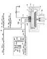
図1は、実施例1による成膜方法を実施する成膜装置を、模式的に示した図である。 FIG. 1 is a diagram schematically illustrating a film forming apparatus that performs the film forming method according to the first embodiment.
本図に示す成膜装置10の概略は、内部に被処理基板Wを収納する処理容器11を有し、当該処理容器11内に形成される処理空間11Aに、ガスライン200およびガスライン100を介して、それぞれ第1の処理ガスおよび第2の処理ガスが供給される構造になっている。 The outline of the
そこで、前記処理空間11Aには、ガスライン200とガスライン100より、処理ガスを1種類ずつ交互に供給することで、処理ガスの反応表面への吸着を経由して原子層・分子層に近いレベルで成膜を行ない、これらの工程を繰り返し、いわゆるALD法により、被処理基板W上に所定の厚さの薄膜を形成することが可能となっている。このようなALD法で形成された膜は、成膜温度が低温でありながら、不純物が少なく高品質な膜質が得られると同時に、微細パターンに成膜するにあたっては、良好なカバレッジ特性を得ることができる。 Therefore, by alternately supplying one type of processing gas from the
従来、このようにガスを交互に供給して成膜する成膜方法(ALD法)では、膜質が良好で、膜質の再現性、成膜の安定性が良好である一方、形成される薄膜の膜質、例えば組成を制御することは困難であった。 Conventionally, a film formation method (ALD method) in which gases are alternately supplied in this way has good film quality, good film quality reproducibility, and good film formation stability. It has been difficult to control film quality, for example composition.
本実施例による成膜方法では、上記の問題を解決し、形成される薄膜に含まれる、金属、窒素、および炭素のうち、少なくともいずれか一つの含有率を制御することが可能となっている。 In the film forming method according to the present embodiment, it is possible to solve the above problems and control the content of at least one of metal, nitrogen, and carbon contained in the formed thin film. .
本実施例による成膜方法では、金属、窒素および炭素を含む第1の処理ガスと、当該第1の処理ガスを還元する第2処理ガスを用いている。また、当該第2の処理ガスによって当該第1の処理ガスを還元する場合、反応が促進されるように、当該第2の処理ガスをプラズマ励起して用いている。そこで、当該第2の処理ガスをプラズマ励起する場合の、高周波電力を変更することにより、形成される薄膜に含有する金属、窒素または炭素の含有率を制御することを可能としている。この成膜方法の詳細については後述する。 In the film forming method according to the present embodiment, a first processing gas containing metal, nitrogen, and carbon and a second processing gas for reducing the first processing gas are used. Further, when the first processing gas is reduced by the second processing gas, the second processing gas is used after being plasma-excited so that the reaction is promoted. Therefore, it is possible to control the content of metal, nitrogen or carbon contained in the formed thin film by changing the high-frequency power when the second processing gas is plasma-excited. Details of this film forming method will be described later.
次に、前記成膜装置10の詳細についてみると、本図に示す成膜装置10は、例えばアルミニウム、表面をアルマイト処理されたアルミニウムもしくはステンレススチールなどからなる処理容器11を有し、前記処理容器11の内部には基板保持台支持部12aに支持された、略円板状の、例えばハステロイからなる基板保持台12が設置され、前記基板保持台12の中心には被処理基板である半導体被処理基板Wが載置される。前記基板保持台12には図示しないヒータが内蔵されて前記被処理基板を所望の温度に加熱することが可能な構造となっている。 Next, regarding the details of the
前記基板処理容器11内の処理空間11Aは、排気口15に接続される、図示しない排気手段により真空排気され、前記処理空間11Aを減圧状態とすることが可能である。また、前記被処理基板Wは、前記処理容器11に設置された図示しないゲートバルブより前記処理容器11内に搬入もしくは搬出される。 The
また、前記処理容器11内には、前記基板保持台12に対向するように、例えばアルミニウムかなる略円筒状のシャワーヘッド部13が設置されており、前記シャワーヘッド部13の側壁面および当該シャワーヘッド部13と前記処理容器11の間には、例えば石英やSiN、AlNなどのセラミックなどからなるインシュレータ16が設けられている。 In addition, a substantially cylindrical
また、前記シャワーヘッド部13上の、前記処理容器11の上の壁面には開口部が設けられて、絶縁体からなるインシュレータ14が挿通されている。前記インシュレータ14には、高周波電源17に接続された導入線17aが挿通され、前記導入線17aは前記シャワーヘッド部13に接続されて、前記導入線17aによって前記シャワーヘッド部13には高周波電源が印加される構造となっている。 In addition, an opening is provided in the wall surface of the
また、前記処理空間11Aに、第1の処理ガスを供給する前記ガスライン200と、前記処理空間11Aに、第2の処理ガスを供給するガスライン100は、前記シャワーヘッド部13に接続され、前記第1の処理ガスと第2の処理ガスは、当該シャワーヘッド部13を介して前記処理空間11Aに供給される構造になっている。また、前記ガスライン200およびガスライン100にはそれぞれ、インシュレータ200aおよび100aが挿入されており、ガスラインが高周波電力から隔絶される構造になっている。 Further, the
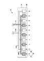
図2は、前記シャワーヘッド部13の詳細を模式的に示した断面図である。ただし図中、先に説明した部分には同一の参照符号を付し、説明を省略する。前記シャワーヘッド部13は、内部に第1の処理ガスのガス流路200Gと、第2の処理ガスのガス流路100Gが形成されたシャワーヘッド本体13Aと、当該シャワーヘッド本体13Aに係合する、複数のガス孔13cおよび13dからなるガス孔13Eが形成されたシャワープレート13Bを有している。 FIG. 2 is a cross-sectional view schematically showing details of the
前記ガスライン200に接続された前記ガス流路200Gは、さらに前記シャワープレート13Bのガス孔13cに接続されている。すなわち、前記第1の処理ガスは、前記ガスライン200から前記ガス流路200G、さらに前記ガス孔13cへかけて構成されている第1のガス供給経路を介して前記処理空間11Aに供給される。一方、前記ガスライン100に接続された前記ガス流路100Gは、さらに前記シャワープレート13Bのガス孔13dに接続されている。すなわち、前記第2の処理ガスは、前記ガスライン100から前記ガス流路100G、さらに前記ガス孔13dへかけて構成されている第2のガス供給経路を介して前記処理空間11Aに供給される。 The
このように、前記シャワーヘッド部13は、第1の処理ガスと第2の処理ガスの流路が独立に形成されており、当該第1の処理ガスと第2の処理ガスはおもに前記処理空間11Aで混合される、いわゆるポストミックス型のシャワーヘッド構造となっている。 In this way, the
また、前記ガスライン200には、当該ガスライン200に第1の処理ガスを供給する、バルブ202aを付されたガスライン202と、前記ガスライン200にパージガスを供給するガスライン201が接続されている。 The
同様に、前記ガスライン100には、当該ガスライン100に第2の処理ガスを供給するガスライン101と、当該ガスライン100にパージガスを供給するガスライン102が接続されている。 Similarly, a
まず、前記ガスライン202についてみると、当該ガスライン202には、バルブ202aを介して、液体原料を気化する気化器203が接続されている。当該気化器203は、ライン204から供給される液体原料を気化して第1の処理ガスとし、当該第1の処理ガスを、ライン207から供給される例えばArなどのキャリアガスと共に、前記ガスライン202からガスライン200に供給する。 First, regarding the
前記気化器203に液体原料を供給する前記ライン204は、液体用質量流量コントローラ204Aと、バルブ204a、204b、204cを有し、原料206Aが保持された、原料容器206に接続されている。当該原料容器206には、例えばアミド化合物である原料、例えばTa(NC(CH3)2C2H5)(N(CH3)2)3などの、金属と窒素および炭素を含む原料が保持され、当該原料は、ガスライン205から供給される、例えばHeなどのガスによって押圧されて、気化器に供給される構造になっている。The
また、前記ガスライン200にパージガスを供給するための前記ガスライン201には、パージガスである、例えば、Arガスの供給源が接続され、質量流量コントローラ201Aと、バルブ201a、201bが付され、供給されるパージガスの流量が制御される構造になっている。 The
一方、前記ガスライン100に接続された、前記ガスライン101には、第2の処理ガスである、例えばH2ガスの供給源が接続され、質量流量コントローラ101Aと、バルブ101a、101bが付されて、前記ガスライン100に供給される第2の処理ガスの流量が制御される構造になっている。On the other hand, the
また、前記ガスライン100にパージガスを供給するための前記ガスライン102には、パージガスである、例えば、Arガスの供給源が接続され、質量流量コントローラ102Aと、バルブ102a、102bが付され、供給されるパージガスの流量が制御される構造になっている。 The
前記成膜装置10を用いて、例えば、前記保持台12上に載置された、前記被処理基板W上に、金属と窒素および炭素を含む膜を形成する場合、成膜装置10は、概ね以下のように制御される。 When the
まず、前記ガスライン200およびシャワーヘッド部13を介して前記処理空間11Aに金属を含む第1の処理ガスを供給する。当該第1の処理ガスが、前記被処理基板上に吸着した後、当該処理空間11Aに残留する当該第1の処理ガスを、前記排気口15より排気する。この場合、パージガスを用いて処理空間11Aをパージしてもよい。 First, a first processing gas containing metal is supplied to the
次に、前記ガスライン100およびシャワーヘッド部13を介して前記処理空間11Aに、前記第1の処理ガスを還元する第2の処理ガスを供給し、さらに前記シャワーヘッド部13に、前記高周波電源17から高周波電力を印加して前記処理空間11Aに、前記第2の処理ガスのプラズマを励起する。このため、当該第2の処理ガスの解離が進行し、解離することにより生成されるラジカルやイオンにより、前記第1の処理ガスの還元が促進される。 Next, a second processing gas for reducing the first processing gas is supplied to the
次に、当該処理空間11Aに残留する当該第2の処理ガスを、前記排気口15より排気する。この場合、パージガスを用いて処理空間11Aをパージしてもよい。 Next, the second processing gas remaining in the
このような処理を繰り返すことにより、すなわち、処理空間に第1の処理ガスを供給して排出し、さらに第2の処理ガスを供給して排出することを、所定の回数繰り返すことで、前記被処理基板W上に、所望の厚さの薄膜が形成される。 By repeating such processing, that is, supplying and discharging the first processing gas to the processing space and supplying and discharging the second processing gas a predetermined number of times are repeated. A thin film having a desired thickness is formed on the processing substrate W.
このようにして、いわゆるALD法により形成された膜は、膜中の不純物が少なく、膜質が良好である特長を有している。 Thus, the film formed by the so-called ALD method has a feature that the film has few impurities and the film quality is good.
従来は、このようなALd法による成膜方法によって薄膜を形成する場合には、薄膜の特性、例えば組成の制御が困難であるという懸念があった。そこで、本実施例では、第2の処理ガスをプラズマ励起する場合の高周波電力を変更することで、形成される薄膜の組成、例えば前記金属、窒素、および炭素のうち、少なくともいずれか一つの含有率を制御することを可能としている。 Conventionally, when a thin film is formed by such a film formation method by the ALd method, there is a concern that it is difficult to control the characteristics of the thin film, for example, the composition. Therefore, in this example, the composition of the thin film to be formed, for example, containing at least one of the metal, nitrogen, and carbon is changed by changing the high-frequency power when plasma-exciting the second processing gas. It is possible to control the rate.
上記のように、第2の処理ガスをプラズマ励起する場合の高周波電力を変更することで、形成される薄膜の組成が制御できる理由を、以下に図3〜図5を用いて説明する。 The reason why the composition of the formed thin film can be controlled by changing the high-frequency power when the second processing gas is plasma-excited as described above will be described below with reference to FIGS.
図3(A)は、Ta(NC(CH3)2C2H5)(N(CH3)2)3の構造を模式的に示した図であり、図3(B)は、本実施例による成膜方法において、Ta(NC(CH3)2C2H5)(N(CH3)2)3が被処理基板Wに吸着した場合の状態を模式的に示した図である。FIG. 3 (A) is a diagram schematically showing the structure of Ta (NC (CH3 )2 C2 H5 ) (N (CH3 )2 )3 , and FIG. in the film forming method according to theexample, Ta (NC (CH 3) 2 C 2 H 5) (N (CH 3) 2) 3 is a diagram schematically showing a state in which adsorbed on the target substrate W.
まず、図3(A)を参照するに、Ta(NC(CH3)2C2H5)(N(CH3)2)3は、Taに、Nが結合し、さらに当該Nに炭素とメチル基が、また当該炭素にはメチル基とエチル基が、図に示すように結合した構造となっている。First, referring to FIG. 3A, Ta (NC (CH3 )2 C2 H5 ) (N (CH3 )2 )3 is bonded to Ta and N is bonded to carbon. It has a structure in which a methyl group and a methyl group and an ethyl group are bonded to the carbon as shown in the figure.
図3(B)を参照するに、本図は、加熱された被処理基板W上に供給されたTa(NC(CH3)2C2H5)(N(CH3)2)3が、被処理基板W上に吸着した状態を示したものであるが、Ta(NC(CH3)2C2H5)(N(CH3)2)3の構造で、結合の弱いC−C2H5の結合が切れ、Cの結合手が被処理基板、または被処理基板上の形成物や付着などと結合すると考えられる。すなわち、本図は、本実施例による成膜方法において、第1の処理ガスを供給した後の被処理基板の状態を模式的に示した図である。Referring to FIG. 3B, this diagram shows that Ta (NC (CH3 )2 C2 H5 ) (N (CH3 )2 )3 supplied on the heated substrate W to be processed is This shows a state of being adsorbed on the substrate to be processed W, but has a structure of Ta (NC (CH3 )2 C2 H5 ) (N (CH3 )2 )3 and weakly bonded C—C2 It is considered that the bond of H5 is broken, and the bond of C is bonded to the substrate to be processed, or a formation or adhesion on the substrate to be processed. That is, this figure is a diagram schematically showing the state of the substrate to be processed after the first processing gas is supplied in the film forming method according to this example.
次に、この状態より、第2の処理ガスである、例えばH2を供給して、当該第2の処理ガスをプラズマ励起し、水素ラジカルや水素イオンによって、基板に吸着したTa(NC(CH3)2C2H5)(N(CH3)2)3の結合手を切る反応を生じさせる。Next, from this state, for example, H2 which is a second processing gas is supplied, the second processing gas is plasma-excited, and Ta (NC (CH (CH3 )2 C2 H5 ) (N (CH3 )2 )3 The reaction of breaking the bond is generated.
この場合、プラズマ励起された第2の処理ガスによって切断されやすいと考えられる、すなわち結合エネルギーが小さい結合は、図3(B)に、結合B1で示した、N−CH3結合である。すなわち、第2の処理ガスをプラズマ励起する場合の高周波電力が小さい場合には、前記結合B1が優先的に切断されると考えられる。In this case, the bond that is considered to be easily cut by the plasma-excited second processing gas, that is, the bond having a small bond energy is an N—CH3 bond indicated by a bond B1 in FIG. That is, it is considered that the coupling B1 is preferentially cut when the high-frequency power when the second processing gas is plasma-excited is small.
一方、プラズマ励起のための高周波電力が大きい場合には、さらに結合エネルギーの大きい結合が切断されるため、例えば、本図に結合B2で示したTa−N結合がさらに切断されると考えられる。このように、プラズマ励起のための高周波電力、本実施例の場合には前記シャワーヘッド部13に印加される高周波電力を制御することにより、被処理基板に吸着した第1の処理ガスの結合状態を任意に変更することが可能となり、そのために形成される薄膜の組成を変更することが可能となる。 On the other hand, when the high frequency power for plasma excitation is large, since the bond having a larger binding energy is cut, for example, it is considered that the Ta-N bond indicated by the bond B2 in this figure is further cut. As described above, the high-frequency power for plasma excitation, in the case of the present embodiment, the high-frequency power applied to the
次に、具体的に、本実施例による成膜方法において、当該高周波電力が大きい場合に形成されると考えられる薄膜(Ta(C)N膜)のモデルと、当該高周波電力が小さい場合に形成されると考えられる薄膜(Ta(C)N膜)のモデルについて、それぞれ図4(A)〜(C)と、図5(A)〜(C)に、模式的に示す。 Next, specifically, in the film forming method according to the present embodiment, a model of a thin film (Ta (C) N film) that is considered to be formed when the high-frequency power is large, and when the high-frequency power is small, is formed. 4 (A) to (C) and FIGS. 5 (A) to (C) schematically show a model of a thin film (Ta (C) N film) considered to be formed.
まず、図4(A)〜(C)は、高周波電力が大きい場合に本発明による成膜方法によって、Ta(C)N膜が形成される状態を、手順を追って模式的に示した図である。 First, FIGS. 4A to 4C are diagrams schematically showing a state in which a Ta (C) N film is formed by a film forming method according to the present invention when high-frequency power is large. is there.
まず、図4(A)に示す状態は、被処理基板上に第1の処理ガスであるTa(NC(CH3)2C2H5)(N(CH3)2)3が供給された後の状態であり、Ta(NC(CH3)2C2H5)(N(CH3)2)3が被処理基板W上に吸着した状態である。First, in the state shown in FIG. 4A, Ta (NC (CH3 )2 C2 H5 ) (N (CH3 )2 )3 as the first processing gas is supplied onto the substrate to be processed. This is a later state in which Ta (NC (CH3 )2 C2 H5 ) (N (CH3 )2 )3 is adsorbed on the substrate W to be processed.
次に、図4(B)に示す状態で、被処理基板上に第2の処理ガスである、例えばH2を供給し、さらにプラズマ励起を行うことで、水素イオンや水素ラジカルを生成し、当該水素イオンや水素ラジカルによって結合を切断し、次に供給されるTa(NC(CH3)2C2H5)(N(CH3)2)3が結合するための、未結手が形成される。Next, in the state shown in FIG. 4B, a second processing gas, for example, H2 is supplied onto the substrate to be processed, and further plasma excitation is performed to generate hydrogen ions and hydrogen radicals. The bond is broken by the hydrogen ion or hydrogen radical, and Ta (NC (CH3 )2 C2 H5 ) (N (CH3 )2 )3 to be supplied next forms a dangling bond. Is done.
この場合、プラズマエネルギー、すなわち高周波電力が大きいために、前記結合B2、すなわちTa―N結合が切断されるため、図に示す未結合手A1が形成される。次に、再び被処理基板W上に、第1の処理ガス、例えばTa(NC(CH3)2C2H5)(N(CH3)2)3が供給された場合に、当該未結合手A1に、図に示すように結合する。In this case, since the plasma energy, that is, the high-frequency power is large, the bond B2, that is, the Ta—N bond is cut, so that the unbonded hand A1 shown in the drawing is formed. Next, when the first processing gas, for example, Ta (NC (CH3 )2 C2 H5 ) (N (CH3 )2 )3 is supplied onto the substrate W again, the unbonded state Join the hand A1 as shown in the figure.
この場合、Ta−N結合が切断されるために、後述する高周波電力が小さい場合に比べて形成される薄膜中のNの含有率が小さくなる。また、後述する高周波電力が小さい場合に比べて形成される薄膜中のCの含有率は高くなり、Taの含有率は低くなる。すなわち、高周波電力を大きくすることで、形成される薄膜中のCの含有率を増大させ、NとTaの含有率を減少させることができる。 In this case, since the Ta—N bond is cut, the N content in the thin film formed is smaller than when the high-frequency power described later is small. In addition, the C content in the thin film formed is higher and the Ta content is lower than when the high-frequency power described later is small. That is, by increasing the high-frequency power, the C content in the formed thin film can be increased, and the N and Ta content can be decreased.
一方、図5(A)〜(C)は、高周波電力が小さい場合に本発明による成膜方法によって、Ta(C)N膜が形成される状態を、手順を追って模式的に示した図である。 On the other hand, FIGS. 5A to 5C are diagrams schematically showing a state in which the Ta (C) N film is formed by the film forming method according to the present invention when the high frequency power is small. is there.
まず、まず、図5(A)に示す状態は、図4(A)に示した状態と同一である。 First, the state shown in FIG. 5A is the same as the state shown in FIG.
次に、図5(B)に示す状態で、被処理基板上に第2の処理ガスである、例えばH2を供給し、さらにプラズマ励起を行うことで、水素イオンや水素ラジカルを生成し、当該水素イオンや水素ラジカルによって結合を切断し、次に供給されるTa(NC(CH3)2C2H5)(N(CH3)2)3が結合するための、未結手が形成される。Next, in the state shown in FIG. 5B, a second processing gas, for example, H2 is supplied onto the substrate to be processed, and further plasma excitation is performed to generate hydrogen ions and hydrogen radicals. The bond is broken by the hydrogen ion or hydrogen radical, and Ta (NC (CH3 )2 C2 H5 ) (N (CH3 )2 )3 to be supplied next forms a dangling bond. Is done.
この場合、プラズマエネルギー、すなわち高周波電力が小さいために、結合エネルギーが小さい結合である前記結合B1、すなわちN−CH3結合が切断されるため、図に示す未結合手A2が形成される。次に、再び被処理基板W上に、第1の処理ガス、例えばTa(NC(CH3)2C2H5)(N(CH3)2)3が供給された場合に、当該未結合手A2に、図に示すように結合する。In this case, since the plasma energy, that is, the high-frequency power is small, the bond B1, which is a bond having a small bond energy, that is, the N—CH3 bond is cut, so that a dangling bond A2 shown in the figure is formed. Next, when the first processing gas, for example, Ta (NC (CH3 )2 C2 H5 ) (N (CH3 )2 )3 is supplied onto the substrate W again, the unbonded state Join the hand A2 as shown.
この場合、N−CH3結合が切断されるため、Ta―N結合は維持され、そのために上記の高周波電力が大きい場合に比べて、形成される薄膜中のNの含有率が大きくなる。また、上記の高周波電力が大きい場合に比べて形成される薄膜中のCの含有率は低くなり、Taの含有率は高くなる。すなわち、高周波電力を小さくすることで、形成される薄膜中のCの含有率を減少させ、NとTaの含有率を増大させることができる。In this case, since the N—CH3 bond is broken, the Ta—N bond is maintained. Therefore, the N content in the formed thin film is increased as compared with the case where the high-frequency power is large. In addition, the C content in the thin film formed is lower and the Ta content is higher than when the high-frequency power is high. That is, by reducing the high-frequency power, the C content in the formed thin film can be reduced, and the N and Ta content can be increased.
次に、本実施例による成膜方法を用いて、前記シャワーヘッド部13に印加する高周波電力を変更して形成したTa(C)N膜の分析結果を図6(A)〜(B)に示す。 Next, the analysis results of the Ta (C) N film formed by changing the high frequency power applied to the
図6(A)は、第1の処理ガスにTa(NC(CH3)2C2H5)(N(CH3)2)3、第2の処理ガスにH2を用いて、第2の処理ガスをプラズマ励起するために前記シャワーヘッド部13に印加する高周波電力を変更した場合に、形成される薄膜に含まれる、Ta、C、Nの含有率の変化を、RBS分析(ラザフォード後方錯乱分光法)によって調べた結果である。FIG. 6A shows a second process using Ta (NC (CH3 )2 C2 H5 ) (N (CH3 )2 )3 as the first process gas and H2 as the second process gas. When the high frequency power applied to the
図6(A)を参照するに、高周波電力を増大させると、Cの含有率が増大し、NとTaの含有率が減少しているのがわかる。また、高周波電力を減少させると、Cの含有率が減少し、NとTaの含有率が増大しているすなわち、高周波電力を変更することで、形成される薄膜の、金属、例えばTaと、N、およびCの含有率を任意に制御することが可能であることが確認された。 Referring to FIG. 6A, it can be seen that when the high frequency power is increased, the C content increases and the N and Ta content decreases. Further, when the high frequency power is reduced, the content of C is decreased and the content of N and Ta is increased. That is, by changing the high frequency power, the metal of the thin film formed, for example, Ta, It was confirmed that the contents of N and C can be arbitrarily controlled.
また、このように薄膜に含まれる元素の含有率を変更することで、例えば当該薄膜の比抵抗を制御することが可能となる。 In addition, by changing the content of elements contained in the thin film in this way, for example, the specific resistance of the thin film can be controlled.
図6(B)は、図6(A)に示した薄膜の膜厚と比抵抗を調べた結果である。図6(B)を参照するに、膜厚は高周波電力を変化させた場合の変化は僅かであり、略一定であることがわかる。一方、薄膜の比抵抗は、高周波電力を大きくするに従い、減少している。これは、図6(A)に示す薄膜の組成の変化が比抵抗に現れたものであり、特にCの含有率が増大することがおもに比抵抗が小さくなる原因と考えられる。すなわち、高周波電力を大きくすることで、形成される薄膜の特性、例えば比抵抗を制御することが可能であり、例えば高周波電力を大きくすることで、比抵抗を小さくすることが可能であることが確認された。また、このように比抵抗が小さい薄膜は、例えば半導体装置の配線であるCuの拡散防止膜として用いると好適である。 FIG. 6B shows the results of examining the thickness and specific resistance of the thin film shown in FIG. Referring to FIG. 6B, it can be seen that the film thickness changes little when the high frequency power is changed, and is substantially constant. On the other hand, the specific resistance of the thin film decreases as the high frequency power increases. This is because the change in the composition of the thin film shown in FIG. 6A appears in the specific resistance, and in particular, the increase in the C content is considered to cause the specific resistance to decrease. That is, by increasing the high frequency power, it is possible to control the characteristics of the thin film to be formed, for example, the specific resistance. For example, by increasing the high frequency power, it is possible to reduce the specific resistance. confirmed. In addition, such a thin film having a small specific resistance is preferably used as a diffusion preventing film for Cu, which is a wiring of a semiconductor device, for example.
また、Cuの拡散防止膜として当該薄膜を用いる場合、Cuの凝集性が良好であることが好ましい。この場合、凝集性が良好であると、良好な特性のCu配線を形成することが可能であり、当該配線はエレクトロマイグレーション耐性が良好となることがわかっている。このように、Cuの凝集性を良好とするためには、Cuの拡散防止膜のNの含有率が高いことが好ましい。本実施例による成膜方法では、高周波電力を小さくして、Cuの拡散防止膜のNの含有率を増大させ、このため、Cuの凝集性を良好としたCuの拡散防止膜を形成することが可能である。 Further, when the thin film is used as a Cu diffusion preventing film, it is preferable that the cohesiveness of Cu is good. In this case, it is known that if the cohesion is good, it is possible to form a Cu wiring having good characteristics, and the wiring has good electromigration resistance. Thus, in order to improve the cohesiveness of Cu, it is preferable that the N content of the Cu diffusion prevention film is high. In the film forming method according to the present embodiment, the high frequency power is reduced, the N content of the Cu diffusion preventing film is increased, and therefore, a Cu diffusion preventing film having good Cu cohesiveness is formed. Is possible.
しかし、従来は、このようにCuの凝集性が良好であって、かつ比抵抗値の小さいCu拡散防止膜を形成することは困難であった。しかし、本実施例による成膜方法によれば、Cuの凝集性が良好であって、かつ比抵抗値の低いCu拡散防止膜を形成することが可能となる。このようなCu拡散防止膜の構造の例を、図7に示す。 Conventionally, however, it has been difficult to form a Cu diffusion barrier film having good Cu cohesiveness and a small specific resistance. However, according to the film forming method of the present embodiment, it is possible to form a Cu diffusion preventing film having good Cu cohesiveness and a low specific resistance value. An example of the structure of such a Cu diffusion prevention film is shown in FIG.
図7は、Cu配線層を含む半導体装置の断面の一部を模式的に示したものである。図8を参照するに、本図に示す半導体装置は、Cu配線層Meと、層間絶縁膜Diを有し、当該Cu配線層Meと層間絶縁膜Diの間には、本実施例による成膜方法により形成された、第1の層L1と、当該第2の層L2を含むCu拡散防止膜Buが形成されている。 FIG. 7 schematically shows a part of a cross section of a semiconductor device including a Cu wiring layer. Referring to FIG. 8, the semiconductor device shown in this figure has a Cu wiring layer Me and an interlayer insulating film Di, and a film is formed between the Cu wiring layer Me and the interlayer insulating film Di according to this embodiment. A Cu diffusion prevention film Bu including the first layer L1 and the second layer L2 formed by the method is formed.
ここで、前記第2の層L2は、前記Cu配線層Meに接する側に形成され、当該第2の層L2を形成する場合には、前記第2の処理ガスを解離する場合の高周波電力を大きくし、形成される膜中のNの含有率を増大させることで、Cuの凝集性が良好となる膜としている。 Here, the second layer L2 is formed on the side in contact with the Cu wiring layer Me, and when the second layer L2 is formed, the high frequency power for dissociating the second processing gas is obtained. By increasing the content of N and increasing the N content in the formed film, the film has good Cu cohesiveness.
一方、前記第1の層L1を形成する場合には、前記第2の処理ガスを解離する場合の高周波電力を小さくし、形成される膜中のCの含有率を増大させることで、形成される膜の比抵抗を小さくしている。この場合、前記Cu拡散防止膜Buの厚さのうち、前記第1の層L1の厚さが厚いと、Cu拡散防止膜Buの比抵抗が小さくなり、好適である。 On the other hand, when the first layer L1 is formed, the first layer L1 is formed by reducing the high frequency power when dissociating the second processing gas and increasing the C content in the formed film. The specific resistance of the film is reduced. In this case, it is preferable that the thickness of the first layer L1 among the thicknesses of the Cu diffusion preventing film Bu is large, because the specific resistance of the Cu diffusion preventing film Bu becomes small.
このように、本実施例による成膜方法では、薄膜の特性を任意に制御し、さらに形成される膜の厚さ方向に対して異なる性質の膜を形成することができる。さらに、この場合、成膜処理において膜の厚さ方向に対して、すなわち成膜の前半から後半にかけて徐々に高周波電力を大きくする、または小さくすることにより、膜の特性、例えば比抵抗や凝集性などの特性を連続的に変化させることが可能となる。このように、膜の厚さ方向で膜の特性の変化の割合が緩やかであると、例えば結晶欠陥や界面での欠陥などが形成されることが抑制され、膜質が良好となり、好適である。 As described above, in the film forming method according to the present embodiment, it is possible to arbitrarily control the characteristics of the thin film and to form a film having different properties with respect to the thickness direction of the formed film. Further, in this case, film characteristics such as specific resistance and cohesiveness can be increased by gradually increasing or decreasing the high-frequency power in the film thickness direction in the film formation process, that is, from the first half to the second half of the film formation. It is possible to continuously change the characteristics such as. As described above, when the rate of change in film characteristics in the thickness direction of the film is gradual, for example, formation of crystal defects or defects at the interface is suppressed, and the film quality is improved.
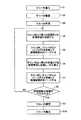
次に、図1に示した成膜装置10を用いて、本実施例の成膜方法を実施する場合の具体的な一例を、図8に示すフローチャートに基づき、説明する。 Next, a specific example in which the film forming method of this embodiment is performed using the
図8は、本実施例による成膜方法を示すフローチャートである。ただし図中、先に説明した部分には同一の参照符号を付し、説明を省略する。 FIG. 8 is a flowchart showing the film forming method according to this embodiment. However, in the figure, the same reference numerals are given to the parts described above, and the description will be omitted.
まず、ステップ1(図中S1と表記する、以下同様)において、被処理基板Wを前記成膜装置10に搬入する。 First, in step 1 (denoted as S1 in the figure, the same applies hereinafter), the substrate to be processed W is carried into the
次に、ステップ2において、前記被処理基板Wを前記基板保持台12に載置する。 Next, in
ステップ3においては、前記保持台12に内蔵したヒータによって前記被処理基板が昇温される。 In step 3, the substrate to be processed is heated by a heater built in the holding table 12.
次にステップ4において、前記バルブ204a、204b、204cを開放し、前記原料容器206から、液体であるTa(NC(CH3)2C2H5)(N(CH3)2)3からなる原料206Aを、液体質量流量コントローラ204Aで流量を制御しながら、前記ライン204から前記気化器203に供給する。Next, in step 4, the
前記気化器203では前記原料206Aを気化して第1の処理ガスとし、当該第1の処理ガスは、前記ガスライン207から前記気化器203に供給されるArと共に、前記ガスライン202から、さらにガスライン200を介して、前記処理空間11Aに供給される。 In the
本ステップにおいて、前記第1の処理ガスが被処理基板上に供給されることで、被処理基板上に前記第1の処理ガスが吸着される。 In this step, when the first processing gas is supplied onto the substrate to be processed, the first processing gas is adsorbed on the substrate to be processed.
また、本ステップにおいては、バルブ102aおよびバルブ102bを開放して前記質量流量コントローラ102Aで流量を制御して、逆流防止ガスとしてArを、前記ガスライン100より前記処理空間11Aに供給し、第1の処理ガスが前記シャワーヘッド部13から、前記ガスライン100の側に逆流することを防止してもよい。 In this step, the valve 102a and the
次に、ステップ5で、前記バルブ204a、204b、204cを閉じて前記処理空間11Aへの前記第1の処理ガスの供給を停止し、前記被処理基板上に吸着していない、未吸着で前記処理空間11Aに残留していた第1の処理ガスを、前記排気口15より前記処理容器11の外へと排出する。この場合、前記バルブ201a、201b、および前記バルブ102a、102bを開放して、それぞれ前記ガスライン200およびガスライン100からパージガスとしてArを導入して、前記処理空間11Aをパージしてもよい。この場合、速やかに残留した第1の処理ガスが処理空間より排出される。所定の時間のパージが終了後、前記バルブ201a、201b、および前記バルブ102a、102bを閉じる。 Next, in
次に、ステップ6において、前記バルブ101aおよび101bを開放し、前記質量流量コントローラ101Aで流量を制御することで、H2ガスを前記ガスライン100より前記処理空間11Aに導入し、さらに、前記高周波電源17より前記シャワーヘッド部13に高周波電力(RF)を印加して、前記処理空間11Aにてプラズマ励起を行う。この場合、前記処理空間のH2が解離されて、H+/H*(水素イオンと水素ラジカル)となり、前記被処理基板W上に吸着している前記第1の処理ガス(Ta(NC(CH3)2C2H5)(N(CH3)2)3)と反応する。この場合、上述したように、シャワーヘッド部13に印加される高周波電力の大きさによって、形成される薄膜の特性、例えば組成を制御することができる。Next, in step 6, the
また、この場合、プラズマを励起する前に、第2の処理ガスの流量安定のため、また処理空間の圧力上昇のために、第2の処理ガスを所定の時間供給するようにしてもよい。 In this case, before the plasma is excited, the second processing gas may be supplied for a predetermined time in order to stabilize the flow rate of the second processing gas and to increase the pressure in the processing space.
また、本ステップにおいては、バルブ201aおよびバルブ201bを開放して前記質量流量コントローラ201Aで流量を制御して、逆流防止ガスとしてArを、前記ガスライン200より前記処理空間11Aに供給し、第2の処理ガスが前記シャワーヘッド部13から、前記ガスライン200の側に逆流することを防止してもよい。 In this step, the
次に、ステップ7で、前記バルブ101a、101bを閉じて前記処理空間11Aへの前記第2の処理ガスの供給を停止し、前記被処理基板上の前記第1の処理ガスと反応していない前記処理空間11Aに残留していた第2の処理ガスを、前記排気口15より前記処理容器11の外へと排出する。この場合、前記バルブ201a、201b、および前記バルブ102a、102bを開放して、それぞれ前記ガスライン200およびガスライン100からパージガスとしてArを導入して、前記処理空間11Aをパージしてもよい。この場合、速やかに残留した第2の処理ガスが処理空間より排出される。所定の時間のパージが終了後、前記バルブ201a、201b、および前記バルブ102a、102bを閉じる。 Next, in step 7, the
次に、ステップ8においては、被処理基板上に必要な膜厚の薄膜を形成するために、成膜工程を再びステップ4に戻し、所望の膜厚となるまでステップ4〜7を繰り返し、必要な回数終了後に次のステップ9に移行する。 Next, in
また、ステップ4〜7の処理を繰り返す場合に、任意の回数の繰り返し処理後に、前記ステップ6において印加される高周波電力を変更して再びステップ4〜7の処理を任意の回数繰り返すことが可能であり、またはステップ4〜7の処理を繰り返す場合に、ステップ6において印加される高周波電力を徐々に増大または減少させるなどの処理を行い、形成される薄膜の特性を、膜厚方向において変更することが可能である。 Further, when the processes in steps 4 to 7 are repeated, it is possible to change the high frequency power applied in step 6 and repeat the processes in steps 4 to 7 again any number of times after an arbitrary number of repetition processes. Yes, or when repeating the processing of Steps 4 to 7, processing such as gradually increasing or decreasing the high-frequency power applied in Step 6 to change the characteristics of the formed thin film in the film thickness direction Is possible.
次に、ステップ9では前記被処理基板Wを前記基板保持台12より離間し、ステップ10で前記処理容器11から前記被処理基板Wを搬出する。 Next, in
また、本実施例においては、処理容器内に供給する第1の処理ガスまたは第2の処理ガスは、上記の例によらず、様々な方法で処理容器内に供給することが可能である。また、第1の処理ガスや第2の処理ガス以外にも、必要に応じて様々なガスを処理容器内に供給することが可能である。 In the present embodiment, the first processing gas or the second processing gas supplied into the processing container can be supplied into the processing container by various methods regardless of the above example. In addition to the first processing gas and the second processing gas, various gases can be supplied into the processing container as necessary.
例えば、第2の処理ガスの一例であるH2ガスは、ステップ4からステップ7にかけて、連続的に処理容器内に供給されるようにしてもよい。H2ガスは、プラズマ励起されるステップ6以外のステップでは、成膜にかかる反応に寄与する割合は僅かであり、実質的に被処理基板上での反応には寄与しないと考えられる。そこで、ステップ4からステップ7にかけて、処理容器内に連続的にH2ガスを供給すると、処理容器内の圧力が安定し、ステップ4からステップ7にかけて実質的に処理容器内の圧力が一定に保持され、成膜処理が安定し、好適である。この場合、前記第1の処理ガスの流量は、前記第2の処理ガスの流量と比べて小さく、第1の処理ガスの供給は実質的な処理容器内の圧力変動に影響は及ぼさない。For example, H2 gas, which is an example of the second processing gas, may be continuously supplied into the processing container from step 4 to step 7. In steps other than step 6 where plasma is excited, H2 gas contributes little to the reaction for film formation, and it is considered that H2 gas does not substantially contribute to the reaction on the substrate to be processed. Therefore, if H2 gas is continuously supplied into the processing container from step 4 to step 7, the pressure in the processing container is stabilized, and the pressure in the processing container is kept substantially constant from step 4 to step 7. Therefore, the film forming process is stable and suitable. In this case, the flow rate of the first processing gas is smaller than the flow rate of the second processing gas, and the supply of the first processing gas does not affect the substantial pressure fluctuation in the processing container.
また、ステップ6においてプラズマ励起をする場合、プラズマの点火が容易となるように、処理容器内の圧力を増大させるように、例えば第2の処理ガスの流量を増大させるようにしてもよい。また、同様にプラズマ点火が容易になるように、処理容器内にArガスを供給するようにしてもよい。また、プラズマ点火後、速やかに上昇させた圧力を元の圧力に戻すための減圧を行う、またはArガスの供給を停止するなど行うと好適である。 Further, when plasma excitation is performed in step 6, for example, the flow rate of the second processing gas may be increased so as to increase the pressure in the processing container so that the plasma can be easily ignited. Similarly, Ar gas may be supplied into the processing container so as to facilitate plasma ignition. In addition, it is preferable to perform pressure reduction for quickly returning the pressure that has been raised to the original pressure after plasma ignition, or to stop the supply of Ar gas.
また、ステップ6においては、成膜処理にかかる反応を促進するため、例えば被処理基板に付着した物質の結合を切断するためのイオンを生成するために、処理容器内にArを供給するようにしてもよい。 Further, in step 6, Ar is supplied into the processing container in order to promote a reaction related to the film forming process, for example, to generate ions for breaking a bond of a substance attached to the substrate to be processed. May be.
このようにして、本実施例よる成膜処理によって、被処理基板上に金属を含む膜、例えばTa(C)N膜が形成される。なお、Ta(C)N膜は、膜中の成分に、Ta、C、N、を少なくとも含む膜であり、その結合状態や含有率が限定されるものではない。 In this manner, a film containing metal, for example, a Ta (C) N film, is formed on the substrate to be processed by the film forming process according to the present embodiment. The Ta (C) N film is a film containing at least Ta, C, and N as components in the film, and its bonding state and content are not limited.
また、本実施例によって形成される金属を含む膜は、不純物が少なく高品質な膜質であり、微細パターンに成膜するにあたっては、良好なカバレッジ特性を得ることができるため、微細化された配線パターンを有する高性能半導体装置の、Cu配線の拡散防止膜(バリア膜または密着膜)に用いると好適である。 In addition, the metal-containing film formed according to this example has a high quality film quality with few impurities, and a fine coverage can be obtained when forming a fine pattern. It is suitable for use as a diffusion preventing film (barrier film or adhesion film) for Cu wiring of a high performance semiconductor device having a pattern.
また、本実施例による成膜方法によって成膜が可能である膜は、Ta(C)N膜などの、Taを含有する膜に限定されず、例えば、Ti、Wなどの金属を含む膜を形成することが可能で有り、Taを含む膜を形成する場合と同様の効果を奏する。 The film that can be formed by the film forming method according to the present embodiment is not limited to a film containing Ta, such as a Ta (C) N film. For example, a film containing a metal such as Ti or W can be used. It can be formed and has the same effect as the case of forming a film containing Ta.
例えば、本実施例による成膜方法によって、Ta(C)N膜、Ti(C)N膜、W(C)N膜などを形成することが可能である。この場合、Ti(C)N膜、および、W(C)N膜は、それぞれ、膜中の成分に、Ti、C、N、およびW、C、Nを少なくとも含む膜であり、その結合状態や含有率が限定されるものではない。 For example, a Ta (C) N film, a Ti (C) N film, a W (C) N film, or the like can be formed by the film forming method according to this embodiment. In this case, the Ti (C) N film and the W (C) N film are films containing at least Ti, C, N, and W, C, N as components in the film, respectively, And the content is not limited.
また、前記第1の処理ガスは、例えばアミド化合物ガスを用いると、膜中に金属、C、Nを含有させることが可能であり、また還元ガスである第2の処理ガスを解離する高周波電力を変更することで、形成される薄膜の組成を変更することが可能であり、好適である。 In addition, when the first processing gas is, for example, an amide compound gas, the film can contain metal, C, and N, and the high-frequency power that dissociates the second processing gas that is a reducing gas. It is possible to change the composition of the thin film to be formed, which is preferable.
例えば、前記アミド化合物ガスは、Ta(NC(CH3)2C2H5)(N(CH3)2)3、Ta[N(C2H5CH3)]5、Ta[N(CH3)2]5、Ta[N(C2H5)2]5、Ta(NC(CH3)3)(N(C2H5)2)3、およびTa(NC(CH3)3)(N(CH3)2)3、Ta(NC2H5)(N(C2H5)2)3、Ta(N(C2H5)2)(N(C2H5)2)3、Ti[N(C2H5CH3)]4、Ti[N(CH3)2]4、およびTi[N(C2H5)2]4よりなる群より選ばれるガスを用いることが可能である。For example, the amide compound gas includes Ta (NC (CH3 )2 C2 H5 ) (N (CH3 )2 )3 , Ta [N (C2 H5 CH3 )]5 , Ta [N (CH3 )2 ]5 , Ta [N (C2 H5 )2 ]5 , Ta (NC (CH3 )3 ) (N (C2 H5 )2 )3 , and Ta (NC (CH3 )3 ) (N (CH3 )2 )3 , Ta (NC2 H5 ) (N (C2 H5 )2 )3 , Ta (N (C2 H5 )2 ) (N (C2 H5 )2 )3 , using a gas selected from the group consisting of Ti [N (C2 H5 CH3 )]4 , Ti [N (CH3 )2 ]4 , and Ti [N (C2 H5 )2 ]4 Is possible.
また、第1の処理ガスは、例えば常温で固体であったり液体であったりまた、気体である場合もあるが、例えば、固体や液体の場合には、必要に応じて加熱して気化させる、または気化器を用いて気化させる、または加熱して昇華させる、などの方法を用いて気化させてガスとして用いればよい。また、固体原料は、溶媒に溶かして一旦液体にし、さらに当該液体を気化させて第1の処理ガスとする方法もある。 In addition, the first processing gas may be solid or liquid at room temperature, or may be a gas. For example, in the case of a solid or liquid, the first processing gas is heated and vaporized as necessary. Alternatively, vaporization may be performed using a vaporizer, or heating and sublimation may be used to form a gas. In addition, there is a method in which the solid raw material is dissolved in a solvent to be once liquid, and the liquid is vaporized to be the first processing gas.
例えば、本実施例で原料206Aの一例としてあげたTa(NC(CH3)2C2H5)(N(CH3)2)3の場合、常温では固体であるが、例えばヘキサン(Hexane)の溶液からなる溶媒に溶解させることにより、常温で液体として扱うことが可能となり、当該液体を図1に示したような気化器を用いて気化し、第1の処理ガスとすることが可能である。なお、図1に示した前記成膜装置10の前記原料容器206には、図示を省略した加熱ヒータが付されており、加熱により固体原料を液体とすることも可能である。For example, in the case of Ta (NC (CH3 )2 C2 H5 ) (N (CH3 )2 )3 given as an example of the
また、本実施例の成膜方法により形成される薄膜は、膜質が良好であり、また膜質、膜厚の均一性が良好であり、微細パターンへのステップカバレッジが良好であって、Cuの拡散防止膜に限定されず、例えば半導体装置を構成する、様々な薄膜として用いることが可能である。 In addition, the thin film formed by the film forming method of this example has good film quality, good film quality, uniform film thickness, good step coverage to a fine pattern, and diffusion of Cu. It is not limited to a prevention film, For example, it can be used as various thin films which comprise a semiconductor device.
以上、本発明を好ましい実施例について説明したが、本発明は上記の特定の実施例に限定されるものではなく、特許請求の範囲に記載した要旨内において様々な変形・変更が可能である。 Although the present invention has been described with reference to the preferred embodiments, the present invention is not limited to the specific embodiments described above, and various modifications and changes can be made within the scope described in the claims.
本発明によれば、金属と窒素と炭素を含む第1の処理ガスと、当該第1の処理ガスを還元する第2の処理ガスを交互に供給して薄膜を形成する成膜方法において、前記薄膜に含まれる、前記金属、窒素、および炭素のうち、少なくともいずれか一つの含有率の制御することが可能となる。 According to the present invention, in the film forming method for forming the thin film by alternately supplying the first processing gas containing metal, nitrogen, and carbon and the second processing gas for reducing the first processing gas, It becomes possible to control the content of at least one of the metal, nitrogen, and carbon contained in the thin film.
10 成膜装置
11 処理容器
12 基板保持台
12a 基板保持台支持
13 シャワーヘッド部
13A シャワーヘッド本体
13B シャワープレート
13c,13d,13E ガス孔
14,16,100a,100b インシュレータ
15 排気口
17 高周波電力
17a 電源ライン
100,101,102,200,201,202,204,207 ガスライン
101A,102A,204A,207A 質量流量コントローラ
101a,101b,102a,102b,202a,204a,204b,204c,207a,207b バルブDESCRIPTION OF
Claims (15)
Translated fromJapanese前記プラズマ励起手段に印加される高周波電力を変更することにより、前記薄膜に含まれる、前記金属、窒素、および炭素のうち、少なくともいずれか一つの含有率を制御することを可能としたことを特徴とする成膜方法。Afirst step of supplying a first processing gas containing metal, nitrogen, and carbon to a processing container provided with a holding table for holding a substrate to be processed; and reducing the first processing gas to theprocessing container And a secondstep of plasma-exciting the second processing gas by means of plasma excitation means provided in the processing container, the first step and the second step A method of forming a thin film on the substrate to be processedby alternately repeating a plurality of steps,
By changing the RF power appliedbefore Symbol plasma excitation means, wherein included in the thin film, the metal, nitrogen, and of the carbon, that made it possible to control at least one of the content A characteristic film forming method.
Priority Applications (2)
| Application Number | Priority Date | Filing Date | Title |
|---|---|---|---|
| JP2004226953AJP4515191B2 (en) | 2004-08-03 | 2004-08-03 | Deposition method |
| US11/180,597US7491430B2 (en) | 2004-08-03 | 2005-07-14 | Deposition method for forming a film including metal, nitrogen and carbon |
Applications Claiming Priority (1)
| Application Number | Priority Date | Filing Date | Title |
|---|---|---|---|
| JP2004226953AJP4515191B2 (en) | 2004-08-03 | 2004-08-03 | Deposition method |
Publications (2)
| Publication Number | Publication Date |
|---|---|
| JP2006045604A JP2006045604A (en) | 2006-02-16 |
| JP4515191B2true JP4515191B2 (en) | 2010-07-28 |
Family
ID=35757729
Family Applications (1)
| Application Number | Title | Priority Date | Filing Date |
|---|---|---|---|
| JP2004226953AExpired - Fee RelatedJP4515191B2 (en) | 2004-08-03 | 2004-08-03 | Deposition method |
Country Status (2)
| Country | Link |
|---|---|
| US (1) | US7491430B2 (en) |
| JP (1) | JP4515191B2 (en) |
Families Citing this family (7)
| Publication number | Priority date | Publication date | Assignee | Title |
|---|---|---|---|---|
| US20030000924A1 (en)* | 2001-06-29 | 2003-01-02 | Tokyo Electron Limited | Apparatus and method of gas injection sequencing |
| JP2006022354A (en)* | 2004-07-06 | 2006-01-26 | Tokyo Electron Ltd | Film-forming method |
| JP5034594B2 (en)* | 2007-03-27 | 2012-09-26 | 東京エレクトロン株式会社 | Film forming apparatus, film forming method, and storage medium |
| JP2011195900A (en)* | 2010-03-19 | 2011-10-06 | Mitsui Eng & Shipbuild Co Ltd | Atomic-layer deposition method and atomic-layer deposition apparatus |
| US10619242B2 (en)* | 2016-12-02 | 2020-04-14 | Asm Ip Holding B.V. | Atomic layer deposition of rhenium containing thin films |
| TWI848974B (en)* | 2018-09-14 | 2024-07-21 | 美商應用材料股份有限公司 | Apparatus for multi-flow precursor dosage |
| KR20210154739A (en) | 2020-06-11 | 2021-12-21 | 에이에스엠 아이피 홀딩 비.브이. | Atomic layer deposition and etching of transition metal dichalcogenide thin films |
Family Cites Families (20)
| Publication number | Priority date | Publication date | Assignee | Title |
|---|---|---|---|---|
| US5306666A (en) | 1992-07-24 | 1994-04-26 | Nippon Steel Corporation | Process for forming a thin metal film by chemical vapor deposition |
| US6699530B2 (en)* | 1995-07-06 | 2004-03-02 | Applied Materials, Inc. | Method for constructing a film on a semiconductor wafer |
| US6345589B1 (en)* | 1996-03-29 | 2002-02-12 | Applied Materials, Inc. | Method and apparatus for forming a borophosphosilicate film |
| US5916365A (en) | 1996-08-16 | 1999-06-29 | Sherman; Arthur | Sequential chemical vapor deposition |
| US6303523B2 (en)* | 1998-02-11 | 2001-10-16 | Applied Materials, Inc. | Plasma processes for depositing low dielectric constant films |
| EP1292970B1 (en)* | 2000-06-08 | 2011-09-28 | Genitech Inc. | Thin film forming method |
| US20020197402A1 (en)* | 2000-12-06 | 2002-12-26 | Chiang Tony P. | System for depositing a film by modulated ion-induced atomic layer deposition (MII-ALD) |
| US6416822B1 (en) | 2000-12-06 | 2002-07-09 | Angstrom Systems, Inc. | Continuous method for depositing a film by modulated ion-induced atomic layer deposition (MII-ALD) |
| US6630201B2 (en)* | 2001-04-05 | 2003-10-07 | Angstron Systems, Inc. | Adsorption process for atomic layer deposition |
| US20020076507A1 (en)* | 2000-12-15 | 2002-06-20 | Chiang Tony P. | Process sequence for atomic layer deposition |
| US6951804B2 (en) | 2001-02-02 | 2005-10-04 | Applied Materials, Inc. | Formation of a tantalum-nitride layer |
| US6828218B2 (en)* | 2001-05-31 | 2004-12-07 | Samsung Electronics Co., Ltd. | Method of forming a thin film using atomic layer deposition |
| US20030017697A1 (en)* | 2001-07-19 | 2003-01-23 | Kyung-In Choi | Methods of forming metal layers using metallic precursors |
| KR100476370B1 (en)* | 2002-07-19 | 2005-03-16 | 주식회사 하이닉스반도체 | Batch type Atomic Layer Deposition and method for insitu-cleaning in the batch type atomic layer deposition |
| US7022605B2 (en)* | 2002-11-12 | 2006-04-04 | Micron Technology, Inc. | Atomic layer deposition methods |
| WO2004112114A1 (en) | 2003-06-16 | 2004-12-23 | Tokyo Electron Limited | Process for depositing film, process for fabricating semiconductor device, semiconductor device and system for depositing film |
| US7186446B2 (en)* | 2003-10-31 | 2007-03-06 | International Business Machines Corporation | Plasma enhanced ALD of tantalum nitride and bilayer |
| JP2006022354A (en)* | 2004-07-06 | 2006-01-26 | Tokyo Electron Ltd | Film-forming method |
| US7314835B2 (en)* | 2005-03-21 | 2008-01-01 | Tokyo Electron Limited | Plasma enhanced atomic layer deposition system and method |
| US7338901B2 (en)* | 2005-08-19 | 2008-03-04 | Tokyo Electron Limited | Method of preparing a film layer-by-layer using plasma enhanced atomic layer deposition |
- 2004
- 2004-08-03JPJP2004226953Apatent/JP4515191B2/ennot_activeExpired - Fee Related
- 2005
- 2005-07-14USUS11/180,597patent/US7491430B2/enactiveActive
Also Published As
| Publication number | Publication date |
|---|---|
| US7491430B2 (en) | 2009-02-17 |
| US20060029748A1 (en) | 2006-02-09 |
| JP2006045604A (en) | 2006-02-16 |
Similar Documents
| Publication | Publication Date | Title |
|---|---|---|
| US8435905B2 (en) | Manufacturing method of semiconductor device, and substrate processing apparatus | |
| JP4651955B2 (en) | Deposition method | |
| JP4823690B2 (en) | Film-forming method and semiconductor device manufacturing method | |
| JP2004064018A (en) | Film formation method | |
| JP2008057042A (en) | Method for forming ruthenium film for metal wiring structure | |
| TW201135841A (en) | Method of manufacturing semiconductor device, substrate processing apparatus and semiconductor device | |
| WO2007007680A1 (en) | Method of forming film and apparatus for film formation | |
| GB2319533A (en) | Methods of forming a barrier layer based on titanium nitride | |
| TW202146688A (en) | Methods of forming molybdenum-containing films deposited on elemental metal films | |
| JP4515191B2 (en) | Deposition method | |
| TWI515326B (en) | Film forming method and plasma film forming device | |
| US7960278B2 (en) | Method of film deposition | |
| JP4031704B2 (en) | Deposition method | |
| JP2006169617A (en) | Film-forming method and storage medium | |
| US20050085058A1 (en) | Methods of forming conductive metal silicides by reaction of metal with silicon | |
| JP2006022354A (en) | Film-forming method | |
| TW201545895A (en) | Cobalt manganese vapor phase deposition | |
| CN100405549C (en) | Film forming method, method for manufacturing semiconductor device, and film forming apparatus | |
| KR100922905B1 (en) | Film forming method, semiconductor device manufacturing method, semiconductor device, program and recording medium | |
| US20070082130A1 (en) | Method for foming metal wiring structure | |
| JP2006052426A (en) | Method for depositing tantalum nitride film | |
| KR101789864B1 (en) | Method for forming metal film and storage medium | |
| TWI843931B (en) | Method for etching or deposition | |
| JP2006013184A (en) | Method for forming boron nitride film |
Legal Events
| Date | Code | Title | Description |
|---|---|---|---|
| A621 | Written request for application examination | Free format text:JAPANESE INTERMEDIATE CODE: A621 Effective date:20070629 | |
| A977 | Report on retrieval | Free format text:JAPANESE INTERMEDIATE CODE: A971007 Effective date:20100222 | |
| A131 | Notification of reasons for refusal | Free format text:JAPANESE INTERMEDIATE CODE: A131 Effective date:20100302 | |
| A521 | Request for written amendment filed | Free format text:JAPANESE INTERMEDIATE CODE: A523 Effective date:20100414 | |
| TRDD | Decision of grant or rejection written | ||
| A01 | Written decision to grant a patent or to grant a registration (utility model) | Free format text:JAPANESE INTERMEDIATE CODE: A01 Effective date:20100511 | |
| A01 | Written decision to grant a patent or to grant a registration (utility model) | Free format text:JAPANESE INTERMEDIATE CODE: A01 | |
| A61 | First payment of annual fees (during grant procedure) | Free format text:JAPANESE INTERMEDIATE CODE: A61 Effective date:20100512 | |
| R150 | Certificate of patent or registration of utility model | Ref document number:4515191 Country of ref document:JP Free format text:JAPANESE INTERMEDIATE CODE: R150 Free format text:JAPANESE INTERMEDIATE CODE: R150 | |
| FPAY | Renewal fee payment (event date is renewal date of database) | Free format text:PAYMENT UNTIL: 20130521 Year of fee payment:3 | |
| R250 | Receipt of annual fees | Free format text:JAPANESE INTERMEDIATE CODE: R250 | |
| R250 | Receipt of annual fees | Free format text:JAPANESE INTERMEDIATE CODE: R250 | |
| R250 | Receipt of annual fees | Free format text:JAPANESE INTERMEDIATE CODE: R250 | |
| R250 | Receipt of annual fees | Free format text:JAPANESE INTERMEDIATE CODE: R250 | |
| R250 | Receipt of annual fees | Free format text:JAPANESE INTERMEDIATE CODE: R250 | |
| LAPS | Cancellation because of no payment of annual fees |