JP4513269B2 - Transflective liquid crystal display device and electronic equipment - Google Patents
Transflective liquid crystal display device and electronic equipmentDownload PDFInfo
- Publication number
- JP4513269B2 JP4513269B2JP2003068321AJP2003068321AJP4513269B2JP 4513269 B2JP4513269 B2JP 4513269B2JP 2003068321 AJP2003068321 AJP 2003068321AJP 2003068321 AJP2003068321 AJP 2003068321AJP 4513269 B2JP4513269 B2JP 4513269B2
- Authority
- JP
- Japan
- Prior art keywords
- film
- light
- liquid crystal
- pixel
- pattern
- Prior art date
- Legal status (The legal status is an assumption and is not a legal conclusion. Google has not performed a legal analysis and makes no representation as to the accuracy of the status listed.)
- Expired - Fee Related
Links
Images


Landscapes
- Liquid Crystal (AREA)
Description
Translated fromJapanese【0001】
【発明の属する技術分野】
本発明は、基板に電気光学物質が保持された半透過・反射型電気光学装置、およびそれを用いた電子機器に関するものである。さらに詳しくは、半透過・反射型電気光学装置に用いた基板への反射面の形成技術に関するものである。
【0002】
【従来の技術】
液晶装置などの電気光学装置は、各種機器の直視型の表示装置として用いられている。このような電気光学装置のうち、反射型あるいは半透過・半反射型のTFTアクティブマトリクス型の液晶装置では、図19および図20に示すように、TFTアレイ基板10の表面にマトリクス状に配列された多数の画素100aの各々に、対向基板20の側から入射してきた外光を対向基板20の方に向けて反射するための光反射膜8aが透明な画素電極9aの下層側に形成されており、対向基板20側から入射した光をTFTアレイ基板10側で反射し、対向基板20側から出射された光によって反射モードで画像を表示する。また、光反射膜8aには、光透過窓8dが形成されており、バックライト装置から出射された光は、光透過窓8dを透過して液晶層に入射して対向基板側から出射することにより透過モードでも画像を表示する。
【0003】
このような電気光学装置において、光反射膜8aで反射された光の方向性が強いと、画像をみる角度で明るさが異なるなどの視野角依存性が顕著に出てくる。そこで、従来は、第2層間絶縁膜5の表面に、アクリル樹脂などの感光性樹脂を厚めに塗布した後、この感光性樹脂をフォトリソグラフィ技術によりパターニングして光反射膜8aの下層側に、突起あるいは孔からなる凹凸を複数、備えた下層側凹凸形成膜13aを形成し、次に、下層側凹凸形成膜13aの表面に上層側凹凸形成膜7aを形成して凹凸をなだらかな形状として、その上層側に形成される光反射膜8aの表面になだらかな形状の光散乱用の凹凸パターン8gを形成している。
【0004】
但し、光反射膜8a表面の凹凸パターン8gを各画素100aで同一とすると、光反射膜8aからの反射光に干渉が発生してしまい、表示の品位が著しく低下するという問題点がある。そこで、凹凸パターン8gの形態を画素100a毎に相違させることが考えられている(例えば、特許文献1)。
【0005】
【特許文献1】
特開平10−123508号公報
【0006】
【発明が解決しようとする課題】
しかしながら、凹凸パターン8gの形態を画素100a毎に相違させても、従来の半透過・反射型の電気光学装置では、光透過窓8dの形成位置が画素100aで揃っているため、結果的に反射領域が画素間で揃ってしまい、画素間での干渉を防止することができないという問題点がある。
【0007】
以上の問題点に鑑みて、本発明の課題は、反射領域からの反射光の干渉を効果的に防止可能な半透過・反射型電気光学装置、および電気機器を提供することにある。
【0008】
【課題を解決するための手段】
上記課題を解決するために、本発明による半透過・反射型液晶表示装置は、一対の基板間に液晶が挟持され、前記液晶を駆動する一対の電極と光反射膜を有すると共にデータ線と走査線の交差に対応して設けられた画素を複数備えた半透過・反射型液晶表示装置であって、前記光反射膜には透過光による表示を行うための光透過窓が設けられ、前記画素は、n×m個の複数の画素からなるユニットを構成し、前記ユニットのn×m個の複数の画素は、当該画素内における前記光透過窓の形成位置パターンが互いに異なり、前記ユニットを複数有し、前記複数のユニットにおける前記光透過窓の形成位置パターンが互いに異なる前記n×m個の画素の配列が、前記複数のユニット間で異なっていることを特徴とする。
【0009】
例えば、前記多数の画素をn×m個の複数画素ずつ、複数のユニットにグループ分けしたときに、当該ユニット内における前記光透過窓の形成位置パターンの配列が前記ユニット間で異なっている。
【0010】
本発明では、光透過窓が画素の各々に複数形成されているとともに、画素内における前記光透過窓の形成位置パターンが複数、存在する。このため、反射領域の形成位置が異なる画素が存在するので、たとえ、凹凸パターンの形態が全画素で共通であったとしても、光反射膜からの反射光の干渉を抑制することができる。
【0011】
本発明において、前記ユニット内では前記光透過窓の形成位置パターンが画素毎に相違していることが好ましい。
【0012】
本発明において、前記ユニット間では、ユニット内における位置が同一の画素における前記光透過窓の形成位置が全て相違していることが好ましい。
【0013】
本発明において、少なくともユニット内では前記画素毎に前記凹凸パターンが異なる形態(形状、サイズ、分布)をもって形成されていることが好ましい。また、前記ユニット内における前記凹凸パターンの配列が前記ユニット間で異なっていることが好ましい。このように構成すると、反射領域の形成位置が画素間で重複している場合でも、同一形状の凹凸パターンが繰り返し、出現するようなことがない。それ故、光反射膜からの反射光に干渉が発生しない。
【0014】
さらに、光透過窓の形成位置パターンが相違するユニットと、凹凸パターンの形態が相違するユニットの画素数を異ならせれば、全て同一ユニットの繰り返しであっても、画素間で透過窓の形成位置パターンと凹凸パターンの形態が一致する画素の出現確立を少なくできる。
【0015】
本発明の別の形態では、電気光学物質を保持する基板にマトリクス状に構成された複数の画素の各々に、突起あるいは孔からなる複数の凹凸が分散した状態に形成された凹凸形成膜と、該凹凸形成膜の上層側に形成された光反射膜とを有し、該光反射膜の表面には前記凹凸形成膜によって光散乱用の凹凸パターンが形成され、かつ、前記光反射膜には、透過光による表示を行うための光透過窓が形成されてなる半透過・反射型電気光学装置において、前記多数の画素の各々で前記光反射膜に対する前記光透過窓の形成位置が相違していることを特徴とする。
【0016】
本発明では、画素毎に光透過窓の形成位置が異なっているため、光透過窓が繰り返し、出現するようなことがない。それ故、光反射膜からの反射光において光透過窓が干渉を発生させない。
【0017】
本発明において、前記多数の画素の各々に前記凹凸パターンが異なる形態(形状、サイズ、分布)をもって形成されていることが好ましい。このように構成すると、同一の凹凸パターンが繰り返し、出現するようなことがない。それ故、光反射膜からの反射光に干渉が発生しない。
【0018】
本発明において、前記凹凸パターンでは、前記凹凸の形状、サイズ、あるいは分布のばらつきが制御されていることが好ましい。このように構成すると、画素間での輝度むらやぎらつきの発生を回避することができる。
【0019】
本発明において、前記光透過窓は、前記凹凸形成膜が形成する凹凸の一部と平面的に重なっていることが好ましい。このように構成すると、設計の段階で凹凸パターンを変更する際、それに伴って、光透過窓の形成位置も変わることになる。それ故、光透過窓の形成位置を画素間で変えるための設計が容易である。
【0020】
この場合、前記光透過窓の面積は、前記凹凸形成膜が形成する凹凸の面積の1.2倍から1.3倍であることが好ましい。すなわち、凹凸周囲の平坦部とも重なるように光透過窓を形成することにより光の利用効率を高めることが好ましい。
【0021】
本発明においては、例えば、前記凹凸形成膜が形成する凹凸の大部分は、画素間で回転移動した位置関係にあるとともに、これらの凹凸と前記光透過窓との相対位置関係は画素間で同一である。このように構成するには、例えば、1つの画素よりも大きな凹凸形成用パターンに光透過窓形成パターンを加えたものを基準パターンとし、当該基準パターンを所定の位置を中心に回転移動させて得たパターンによって、各画素に対し、前記凹凸の位置、および前記光透過窓の位置を決定する。
【0022】
また、本発明において、前記凹凸形成膜が形成する凹凸の大部分は、画素間で平行移動した位置関係にあるとともに、これらの凹凸と前記光透過窓との相対位置関係は画素間で同一である構成を採用してもよい。このように構成するには、例えば、左端と右端のパターンおよび上端と下端のパターンがそれぞれ連続性を有した凹凸形成用パターンに光透過窓形成用パターンを加えた矩形の基本パターンを準備し、この基本パターンからの切り出し領域を端部でのパターンの連続性を保ちつつ上下左右に平行移動して得た複数の凹凸パターンによって、前記画素に対し、前記凹凸および前記光透過窓の位置を決定すればよい。
【0023】
本発明においては、光透過窓の形成位置パターンを変えても、光透過窓の形成面積については前記画素間で等しいことが好ましい。
【0024】
本発明においては、前記基板を第1の基板とし、該第1の基板に対して第2の基板を対向配置させて当該基板間に前記電気光学物質としての液晶を保持させて半透過・反射型電気光学装置を構成する。
【0025】
このような半透過・反射型電気光学装置は、例えば、携帯電話機あるいはモバイルコンピュータなどといった電子機器の表示部として用いられる。
【0026】
【発明の実施の形態】
図面を参照して、本発明の実施の形態を説明する。
【0027】
(半透過・反射型電気光学装置の基本的な構成)
図1は、本発明を適用した半透過・反射型電気光学装置を各構成要素とともに対向基板の側から見た平面図であり、図2は、図1のH−H′断面図である。図3は、半透過・反射型電気光学装置の画像表示領域においてマトリクス状に形成された複数の画素における各種素子、配線等の等価回路図である。なお、本形態の説明に用いた各図では、各層や各部材を図面上で認識可能な程度の大きさとするため、各層や各部材毎に縮尺を異ならしめてある。
【0028】
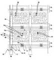
図1および図2において、本形態の半透過・反射型電気光学装置100(液晶装置)は、TFTアレイ基板10(第1の基板)と対向基板20(第2の基板)とがシール材52によって貼り合わされ、このシール材52によって区画された領域(液晶封入領域)内には、電気光学物質としての液晶50が挟持されている。シール材52の形成領域の内側領域には、遮光性材料からなる周辺見切り53が形成されている。シール材52の外側の領域には、データ線駆動回路101、および実装端子102がTFTアレイ基板10の一辺に沿って形成されており、この一辺に隣接する2辺に沿って走査線駆動回路104が形成されている。TFTアレイ基板10の残る一辺には、画像表示領域の両側に設けられた走査線駆動回路104の間をつなぐための複数の配線105が設けられており、更に、周辺見切り53の下などを利用して、プリチャージ回路や検査回路が設けられることもある。また、対向基板20のコーナー部の少なくとも1箇所においては、TFTアレイ基板10と対向基板20との間で電気的導通をとるための基板間導通材106が形成されている。
【0029】
なお、データ線駆動回路101および走査線駆動回路104をTFTアレイ基板10の上に形成する代わりに、たとえば、駆動用LSIが実装されたTAB(テープ オートメイテッド、ボンディング)基板をTFTアレイ基板10の周辺部に形成された端子群に対して異方性導電膜を介して電気的および機械的に接続するようにしてもよい。なお、半透過・反射型電気光学装置100では、使用する液晶50の種類、すなわち、TN(ツイステッドネマティック)モード、STN(スーパーTN)モード等々の動作モードや、ノーマリホワイトモード/ノーマリブラックモードの別に応じて、偏光フィルム、位相差フィルム、偏光板などが所定の向きに配置されるが、ここでは図示を省略してある。
【0030】
また、半透過・反射型電気光学装置100をカラー表示用として構成する場合には、対向基板20において、TFTアレイ基板10の各画素電極(後述する)に対向する領域にRGBのカラーフィルタをその保護膜とともに形成する。
【0031】
このような構造を有する半透過・反射型電気光学装置100の画像表示領域においては、図3に示すように、複数の画素100aがマトリクス状に構成されているとともに、これらの画素100aの各々には、画素電極9a、およびこの画素電極9aを駆動するための画素スイッチング用のTFT30が形成されており、画素信号S1、S2・・・Snを供給するデータ線6aが当該TFT30のソースに電気的に接続されている。データ線6aに書き込む画素信号S1、S2・・・Snは、この順に線順次に供給しても構わないし、相隣接する複数のデータ線6a同士に対して、グループ毎に供給するようにしてもよい。また、TFT30のゲートには走査線3aが電気的に接続されており、所定のタイミングで、走査線3aにパルス的に走査信号G1、G2・・・Gmをこの順に線順次で印加するように構成されている。画素電極9aは、TFT30のドレインに電気的に接続されており、スイッチング素子であるTFT30を一定期間だけそのオン状態とすることにより、データ線6aから供給される画素信号S1、S2・・・Snを各画素に所定のタイミングで書き込む。このようにして画素電極9aを介して液晶に書き込まれた所定レベルの画素信号S1、S2、・・・Snは、図2に示す対向基板20の対向電極21との間で一定期間保持される。
【0032】
ここで、液晶50は、印加される電圧レベルにより分子集合の配向や秩序が変化することにより、光を変調し、階調表示を可能にする。ノーマリーホワイトモードであれば、印加された電圧に応じて入射光がこの液晶50の部分を通過する光量が低下し、ノーマリーブラックモードであれば、印加された電圧に応じて入射光がこの液晶50の部分を通過する光量が増大していく。その結果、全体として半透過・反射型電気光学装置100からは画素信号S1、S2、・・・Snに応じたコントラストを持つ光が出射される。
【0033】
なお、保持された画素信号S1、S2、・・・Snがリークするのを防ぐために、画素電極9aと対向電極との間に形成される液晶容量と並列に蓄積容量60を付加することがある。例えば、画素電極9aの電圧は、ソース電圧が印加された時間よりも3桁も長い時間だけ蓄積容量60により保持される。これにより、電荷の保持特性は改善され、コントラスト比の高い半透過・反射型電気光学装置100が実現できる。なお、蓄積容量60を形成する方法としては、図3に例示するように、蓄積容量60を形成するための配線である容量線3bとの間に形成する場合、あるいは前段の走査線3aとの間に形成する場合もいずれであってもよい。
【0034】
(TFTアレイ基板の構成)
図4は、本形態の半透過・反射型電気光学装置に用いたTFTアレイ基板の相隣接する複数の画素群の平面図である。図5は、半透過・反射型電気光学装置の画素の一部を図4のA−A′線に相当する位置で切断したときの断面図である。
【0035】
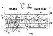
図4において、TFTアレイ基板10上には、複数の透明なITO(Indium Tin Oxide)膜からなる画素電極9aがマトリクス状に形成されており、これら各画素電極9aに対して画素スイッチング用のTFT30がそれぞれ接続している。また、画素電極9aの縦横の境界に沿って、データ線6a、走査線3a、および容量線3bが形成され、TFT30は、データ線6aおよび走査線3aに対して接続している。すなわち、データ線6aは、コンタクトホールを介してTFT30の高濃度ソース領域1dに電気的に接続し、画素電極9aは、コンタクトホールを介してTFT3の高濃度ドレイン領域1eに電気的に接続している。また、TFT30のチャネル領域1a′に対向するように走査線3aが延びている。なお、蓄積容量60(蓄積容量素子)は、画素スイッチング用のTFT30を形成するための半導体膜1の延設部分1fを導電化したものを下電極とし、この下電極41に、走査線3bと同層の容量線3bが上電極として重なった構造になっている。
【0036】
このように構成した各画素100aには、後述するように、画素電極9aの下層側に、この画素電極9aと略重なる領域に光反射膜8aが形成されている。
【0037】
画素100aのA−A′線における断面は、図5に示すように、TFTアレイ基板10の基体たる透明な基板10′の表面に、厚さが300nm〜500nmのシリコン酸化膜(絶縁膜)からなる下地保護膜11が形成され、この下地保護膜11の表面には、厚さが50nm〜100nmの島状の半導体膜1aが形成されている。半導体膜1aの表面には、厚さが約50〜150nmのシリコン酸化膜からなるゲート絶縁膜2aが形成され、このゲート絶縁膜2aの表面に、厚さが300nm〜800nmの走査線3aがゲート電極として通っている。半導体膜1aのうち、走査線3aに対してゲート絶縁膜2aを介して対峙する領域がチャネル領域1a′になっている。このチャネル領域1a′に対して一方側には、低濃度ソース領域1bおよび高濃度ソース領域1dを備えるソース領域が形成され、他方側には低濃度ドレイン領域1cおよび高濃度ドレイン領域1eを備えるドレイン領域が形成されている。
【0038】
画素スイッチング用のTFT30の表面側には、厚さが300nm〜800nmのシリコン酸化膜からなる第1層間絶縁膜4、および厚さが100nm〜300nmのシリコン窒化膜からなる第2層間絶縁膜5(表面保護膜)が形成されている。第1層間絶縁膜4の表面には、厚さが300nm〜800nmのデータ線6aが形成され、このデータ線6aは、第1層間絶縁膜4に形成されたコンタクトホールを介して高濃度ソース領域1dに電気的に接続している。第1層間絶縁膜4の表面にはデータ線6aと同時形成されたドレイン電極6bが形成され、このドレイン電極6bは、第1層間絶縁膜4に形成されたコンタクトホールを介して高濃度ドレイン領域1eに電気的に接続している。
【0039】
第2層間絶縁膜5の上層には、有機系樹脂などの感光性樹脂からなる下層側凹凸形成膜13a、およびポリシラザンや有機系樹脂などからなる上層側凹凸形成膜7aがこの順に形成され、上層側凹凸形成膜7aの表面には、アルミニウム膜などからなる光反射膜8aが形成されている。
【0040】
ここで、光透過膜8aには、透過モードでの表示を行うための光透過窓8dが形成され、本形態において、光透過窓8dは、凹凸を形成する下層側凹凸形成膜13aの一部と重なる位置に形成されている。
【0041】
光反射膜8aの上層には、ITO膜からなる透明な画素電極9aが形成されている。画素電極9aは、光反射膜8aの表面に直接、積層され、画素電極9aと光反射膜8aとは電気的に接続されている。また、画素電極9aは、上層側凹凸形成膜7aおよび第2層間絶縁膜5に形成されたコンタクトホール5bを介してドレイン電極6bに電気的に接続している。ここで、光反射膜8aは、コンタクトホール5b内には形成されていないが、画素電極9aに接しており、実質、画素電極9aおよびコンタクトホール5bを介してドレイン電極6bに電気的に接続している状態にある。
【0042】
画素電極9aの表面側にはポリイミド膜からなる配向膜12が形成されている。この配向膜12は、ポリイミド膜に対してラビング処理が施された膜である。
【0043】
また、高濃度ドレイン領域1eからの延設部分1f(下電極)に対しては、ゲート絶縁膜2aと同時形成された絶縁膜(誘電体膜)を介して、走査線3aと同層の容量線3bが上電極として対向することにより、蓄積容量60が構成されている。
【0044】
なお、TFT30は、好ましくは上述のようにLDD構造をもつが、低濃度ソース領域1b、および低濃度ドレイン領域1cに相当する領域に不純物イオンの打ち込みを行わないオフセット構造を有していてもよい。また、TFT30は、ゲート電極(走査線3aの一部)をマスクとして高濃度で不純物イオンを打ち込み、自己整合的に高濃度のソースおよびドレイン領域を形成したセルフアライン型のTFTであってもよい。
【0045】
また、本形態では、TFT30のゲート電極(走査線3a)をソース−ドレイン領域の間に1個のみ配置したシングルゲート構造としたが、これらの間に2個以上のゲート電極を配置してもよい。この際、各々のゲート電極には同一の信号が印加されるようにする。このようにデュアルゲート(ダブルゲート)、あるいはトリプルゲート以上でTFT30を構成すれば、チャネルとソース−ドレイン領域の接合部でのリーク電流を防止でき、オフ時の電流を低減することが出来る。これらのゲート電極の少なくとも1個をLDD構造或いはオフセット構造にすれば、さらにオフ電流を低減でき、安定したスイッチング素子を得ることができる。
【0046】
(凹凸パターン8gの構成)
図4および図5において、TFTアレイ基板10では、各画素100aの反射領域には、光反射膜8aの表面のうち、TFT30の形成領域から外れた領域(光反射膜形成領域)には、凸部8bおよび凹部8cを備えた凹凸パターン8gが形成されている。
【0047】
このような凹凸パターン8gを構成するにあたって、本形態のTFTアレイ基板10では、光反射膜8aの下層側のうち、光反射膜8aと平面的に重なる領域には、有機系の感光性樹脂からなる下層側凹凸形成膜13aが第2層間絶縁膜5の表面に複数の柱状突起(凹凸)として所定の分布をもって形成され、この下層側凹凸形成膜13aの上層には、ポリシラザンや有機系樹脂などといった流動性材料から形成された絶縁膜からなる上層側凹凸形成膜7aが積層されている。このため、反射膜8aの表面には、下層側凹凸形成膜13aの凹凸に対応する凹凸パターン8gが形成され、この凹凸パターン8gでは、上層側凹凸形成膜7aによって、下層側凹凸形成膜13aのエッジなどが出ないようになっている。
【0048】
なお、上層側凹凸形成膜7aを形成せずに、下層側凹凸形成膜13aを形成した後、ベーク工程を行うことにより、下層側凹凸形成膜13aの凹凸(孔13b)の縁を滑らかにすることもある。
【0049】
ここで、下層側凹凸形成膜13aにおいて凹凸を形成する柱状突起は、円形、あるいは略多角形の平面形状を有している。また、下層側凹凸形成膜13aにおいて凹凸を形成する柱状突起は、平面的なサイズが異なるものが複数種類が形成されているが、図4および図5には、同一サイズで図示してある。
【0050】
このように凹凸パターン8gの形状、サイズ及び分布は、柱状突起を構成する下層側凹凸形成膜13aの形状、サイズ及び分布によって規定される。
【0051】
(対向基板の構成)
図5において、対向基板20では、TFTアレイ基板10に形成されている画素電極9aの縦横の境界領域と対向する領域にブラックマトリクス、あるいはブラックストライプなどと称せられる遮光膜23が形成され、その上層側には、ITO膜からなる対向電極21が形成されている。また、対向電極21の上層側には、ポリイミド膜からなる配向膜22が形成され、この配向膜22は、ポリイミド膜に対してラビング処理が施された膜である。
【0052】
(TFTの製造方法)
本形態に係るTFTアレイ基板10を製造する方法を、図6および図7を参照して説明する。
【0053】
図6および図7はいずれも、本形態のTFTアレイ基板11の製造方法を示す工程断面図であり、いずれの図においても、TFT形成領域、および光反射膜形成領域の断面を示してある。
【0054】
なお、本形態のTFTアレイ基板10を製造するにあたって、TFT30などの製造工程は、いわゆる低温プロセスと称せられる方法が採用され、このような方法については、すでに周知であるため、本形態のTFTアレイ基板10の特徴と関連する工程のみを説明する。
【0055】
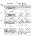
本形態のTFTアレイ基板10を製造するにあたっては、図6(A)に示すように、ガラス製等の基板10′の表面にTFT30を形成した以降、第2層間絶縁膜5にコンタクトホール5bを形成する。
【0056】
次に、第2層間絶縁膜5の表面に、有機系の感光性樹脂13を厚めに塗布した後、感光性樹脂13を露光マスク510を介して露光する。ここで、感光性樹脂13としてはネガタイプおよびポジタイプのいずれを用いてもよいが、図6(A)には、感光性樹脂13としてポジタイプの場合を例示してあり、感光性樹脂13を除去したい部分に対して、露光マスク510の透光部分511を介して紫外線が照射される。
【0057】
次に、露光した感光性樹脂13を現像して、図6(B)に示すように、光反射膜8aの下層側のうち、光反射膜8aと平面的に重なる領域に、図5を参照して説明した柱状突起、、およびコンタクトホール5bを備えた下層側凹凸形成膜13aを形成する。
【0058】
次に、図6(C)に示すように、第2層間絶縁膜5および下層側凹凸形成膜13aの表面側に、ペルヒドロポリシラザンまたはこれを含む組成物を塗布した後、焼成して、あるいは有機系樹脂からなる流動性材料7を塗布した後、図6(D)に示すように、フォトリソグラフィ技術を利用してのパターニング、あるいは露光、現像により、コンタクトホール5bを備えた上層側凹凸形成膜7aを形成する。
【0059】
なお、ペルヒドロポリシラザンとは無機ポリシラザンの一種であり、大気中で焼成することによってシリコン酸化膜に転化する塗布型コーティング材料である。たとえば、東燃(株)製のポリシラザンは、−(SiH2 NH)−を単位とする無機ポリマーであり、キシレンなどの有機溶剤に可溶である。従って、この無機ポリマーの有機溶媒溶液(たとえば、20%キシレン溶液)を塗布液としてスピンコート法(たとえば、2000rpm、20秒間)で塗布した後、450℃の温度で大気中で焼成すると、水分や酸素と反応し、CVD法で成膜したシリコン酸化膜と同等以上の緻密な非晶質のシリコン酸化膜を得ることができる。
【0060】
ここで、上層側凹凸形成膜7aは、流動性を有する材料を塗布したものから形成されるため、上層側凹凸形成膜7aの表面には、下層側凹凸形成膜13aの凹凸を適度に打ち消して、エッジのない、なだらかな形状の凹凸パターン8gが形成される。
【0061】
なお、上層側凹凸形成膜7aを形成せずに、なだらかな形状の凹凸パターン8gを形成する場合には、図6(B)に示す状態でベーク工程を行って、下層側凹凸形成膜13aの縁を滑らかな形状にすればよい。
【0062】
次に、図7(A)に示すように、スパッタ法などによって、上層側凹凸形成膜7aの表面にアルミニウム膜などといった反射性を備えた金属膜8を形成した後、フォトリソグラフィ技術を用いてレジストマスク557を形成する。
【0063】
次に、レジストマスク557を介して金属膜8にエッチングを行い、図7(B)に示すように、所定領域に光反射膜8aを残す。このようにして形成した光反射膜8aの表面には、下層側凹凸形成膜13aの孔13bからなる凹凸によって500nm以上、さらには800nm以上の凹凸パターン8gが形成され、かつ、この凹凸パターン8gは、上層側凹凸形成膜7aによって、エッジのない、なだらかな形状になっている。
【0064】
また、この工程では、光透過膜8aのうち、凹凸を形成する下層側凹凸形成膜13aの一部と重なる位置に光透過窓8dを形成する。
【0065】
次に、図7(C)に示すように、光反射膜8aの表面側に、厚さが40nm〜200nmのITO膜9をスパッタ法などで形成した後、フォトリソグラフィ技術を用いてレジストマスク558を形成する。
【0066】
次に、レジストマスク558を介してITO膜9にエッチングを行って、図7(D)に示すように、ドレイン電極6bに電気的に接続する画素電極9aを形成する。
【0067】
しかる後には、図5に示すように、画素電極9aの表面側にポリイミド膜(配向膜12)を形成する。それには、ブチルセロソルブやn−メチルピロリドンなどの溶媒に5〜10重量%のポリイミドやポリアミド酸を溶解させたポリイミド・ワニスをフレキソ印刷した後、加熱・硬化(焼成)する。そして、ポリイミド膜を形成した基板をレーヨン系繊維からなるパフ布で一定方向に擦り、ポリイミド分子を表面近傍で一定方向に配列させる。その結果、後で充填した液晶分子とポリイミド分子との相互作用により液晶分子が一定方向に配列する。
【0068】
その結果、TFTアレイ基板10が完成する。
【0069】
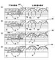
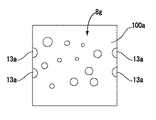
(凹凸パターン8gと画素110aとの関係)
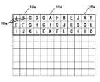
図8は、TFTアレイ基板上において多数の画素を複数画素ずつ、複数のユニットにグループ分けしたときに、少なくともユニット内では画素毎に凹凸パターンが異なる形態をもって形成されているとともに、ユニット内における各凹凸パターンの位置がユニット間で異なっている様子を示す説明図である。図9、図10、および図11は、本形態の半透過・反射型電気光学装置のTFTアレイ基板に付した凹凸パターンの説明図である。図12は、凹凸の相対距離関係を評価するためのドロネイ三角形の説明図である。
【0070】
本形態の半透過・反射型電気光学装置100では、画素電極9aの下層側にアルミニウム膜などからなる光反射膜8aが形成されている。このため、対向基板20側から入射した光をTFTアレイ基板10側で反射し、対向基板20側から出射することができるので、この間に液晶50によって各画素100a毎で光変調を行えば、外光を利用して所望の画像を表示することができる(反射モード)。
【0071】
また、光反射膜8aには、光透過窓8dが形成されており、バックライト装置から出射された光は、光透過窓8dを透過して液晶層に入射して対向基板側から出射することにより透過モードでも画像を表示する。
【0072】
また、本形態では、光反射膜8aの下層側のうち、光反射膜8aと平面的に重なる領域に下層側凹凸形成膜13aを形成し、この下層側凹凸形成膜13aに対応する凹凸を利用して、光反射膜8aの表面に光散乱用の凹凸パターン8gを形成している。また、凹凸パターン8gでは、上層側凹凸形成膜7aによって、下層側凹凸形成膜13aのエッジなどが出ないようになっている。従って、反射モードで画像を表示したとき、散乱反射光で画像を表示するため、視野角依存性が小さい。
【0073】
但し、光反射膜8a表面の凹凸パターン8gを各画素100aで完全同一とすると、光反射膜8aからの反射光に干渉が発生してしまう。
【0074】
そこで、本形態では、まず、図8に示すように、マトリクス状に形成された多数の画素100aをn×m個の複数画素ずつ、複数のユニット101a、102a、103a・・にグループ分けし、少なくともユニット101a、102a、103a・・内では画素100a毎に、凹凸パターン8gが異なる形態をもって形成された構成としている。
【0075】
すなわち、各画素100aに下層側凹凸形成膜13aを形成する際、ユニット101a、102a、103a・・に属する各画素100aに対して、下層側凹凸形成膜13aが形成する柱状突起(凹凸)の形状、サイズ、分布を変えた凹凸パターン8g(凹凸パターンA〜L)を形成するように、露光マスク510を設計してある。
【0076】
ここで、凹凸は、平面的なサイズが異なるものが複数種類が形成されているが、図4および図5には、同一サイズで図示してある。
【0077】
また、ユニット101a、102a、103a・・内における各凹凸パターンA〜Lの位置をユニット101a、102a、103a・・間で異ならせてある。すなわち、第1番目のユニット101aでは、例えば、上段で左から右に向かって凹凸パターンA、凹凸パターンB、凹凸パターンC・・と並んでるのに対して、第2番目のユニット102aでは、上段で左から右に向かって凹凸パターンG、凹凸パターンA、凹凸パターンH・・と並び、第3番目のユニット103aでは、上段で左から右に向かって凹凸パターンE、凹凸パターンJ、凹凸パターンA・・と並んでいる。
【0078】
しかも、ユニット101a、102a、103a・・間では、ユニット内における位置が同一の画素100aにおける光透過窓8dの形成位置が全て相違している。
【0079】
このような複数種類の凹凸パターンを形成するにあたっては、図6(A)に示した露光マスク510を設計する際、本形態では、例えば、図9(A)に示す画素100aを基準画素100a′とし、この基準画素100a′に形成される凹凸パターンAの凹凸を、画素領域内の所定の位置O1を中心に矢印Xで示すように回転移動させ、それにより得られる図9(B)、(C)に示すような凹凸パターンB、C・・を他の画素100aに形成することにより、各画素100aに異なる凹凸パターン8gを形成する。
【0080】
ここで、回転中心O1は、画素領域内に設定されているが、このような場合、凹凸を構成する下層側凹凸形成膜13aの中心からずれた位置に回転中心を設定することが好ましい。また、回転中心を下層側凹凸形成膜13aの外周を規定する円上からずれた位置に設定することが好ましい。このように設定すると、各凹凸パターンA〜Lにおいて、回転中心となった箇所に下層側凹凸形成膜13aが形成されてしまうのを防止することができる。
【0081】
また、露光マスク510を設計する際、図10(A)に示す画素100aを基準画素100a′とし、この基準画素100a′に形成される凹凸パターンAの凹凸を、画素領域外の所定の位置O2を中心に矢印Xで示すように回転移動させ、それにより得られる図10(B)、(C)に示すような凹凸パターンB、C・・を他の画素100aに形成することにより、各画素100aに異なる凹凸パターン8gを形成してもよい。
【0082】
さらに、露光マスク510を設計する際、図11(A)に示す画素100aを基準画素100a′とし、この基準画素100a′に形成される凹凸パターンAの凹凸を、画素領域内のコンタクトホール5bの形成位置O3を中心に矢印Xで示すように回転移動させ、それにより得られる図11(B)、(C)に示すような凹凸パターンB、C・・を他の画素100aに形成することにより、各画素100aに異なる凹凸パターン8gを形成してもよい。この場合も、図5を参照して説明したように、光反射膜8aがコンタクトホール5b内に形成されていないので、画素100aの配列方向でコンタクトホール5bが繰り返し出現してきても、光反射膜8aからの反射光に干渉が発生しない。
【0083】
このような構成のTFTアレイ基板10を用いた半透過・反射型電気光学装置100では、ユニット101a、102a、103a・・内で画素100a毎に凹凸パターン8gが異なる形態をもって形成されているとともに、ユニット内における各凹凸パターン8gの位置がユニット101a、102a、103a・・間で異なっているため、同一の凹凸パターン8gが繰り返し、出現するようなことがない。それ故、光反射膜8aからの反射光に干渉が発生しない。
【0084】
また、本形態では、各画素100aに対して、形態の異なる凹凸パターン8gを形成するにあたって、基準画素100a′に形成されている凹凸を所定の位置を中心に回転移動させた凹凸パターン8gを他の画素100aに形成している。このため、本形態によれば、各画素100aにおいて、下層側凹凸形成膜13aの形状、サイズ、あるいは分布のばらつきが制御されている。すなわち、本形態では、基準画素100aの凹凸を回転させた上で転写したものに相当するため、基準画素100aに形成された下層側凹凸形成膜13aの形状、サイズ、あるいは分布のばらつきは、他の画素100aでも同様なレベルであり、ばらつきが小さい。
【0085】
また、本形態において、下層側凹凸形成膜13aは、1画素内に平面的なサイズの異なる複数種類が形成されているが、このような1画素内での同一サイズの下層側凹凸形成膜13aの数は、画素間で等しい。
【0086】
また、下層側凹凸形成膜13aの側面に形成される斜面の傾きが所定の角度範囲内に収まる凹凸の割合、例えば、凹凸の側面に形成される斜面の傾きが所定の角度範囲内に収まる凹凸の割合は、画素100a間で5%以内のばらつきである。
【0087】
さらに、下層側凹凸形成膜13aが形成されている面積のばらつきは、画素100a間で10%以内である。
【0088】
さらにまた、図12(A)に示すように、複数の下層側凹凸形成膜13aの中心の位置座標からドロネイ図を描いたとき、ドロネイ線の長さ(=中心座標の近接距離)のばらつきが画素100a間で10%以内である。
【0089】
それ故、TFTアレイ基板10に対する法線方向から10度ないし30度、傾いた方向からみたときの反射輝度のばらつきが、パターン間で5%以内であるなど、画素間での輝度むらやぎらつきの発生を回避することができる。
【0090】
ここで、下層側凹凸形成膜13aの平面形状が円形の場合には、図12(A)に示すように、円の中心同士を結んだ線のばらつきを制御するが、図12(B)に示すように、下層側凹凸形成膜13aの平面形状が多角形の場合、その重心同士を結んだ線のばらつきを制御すればよい。
【0091】
なお、図13に示すように、画素100aの端部で下層側凹凸形成膜13aが途切れたパターンとなる場合には、途切れた部分を反対側の辺に出現させて、下層側凹凸形成膜13aの面積の合計が、このサイズの下層側凹凸形成膜13aの正規の面積の整数倍であることが好ましい。このように構成すると、画素100aの端部で下層側凹凸形成膜13aが途切れた場合でも、1画素内に形成されている下層側凹凸形成膜13aの数、および面積を実質、同一とすることができる。
【0092】
(光透過窓8dと画素100aとの関係)
また、本形態では、図8〜図11を参照して説明した凹凸パターンの設計手法をそのまま利用して、図4に示すように、光反射膜8aに対する光透過窓8dの形成位置を各画素100aで相違させてある。従って、TFTアレイ基板10上には、画素100a内における光透過窓8dの形成位置パターンが複数、存在する。
【0093】
すなわち、各画素100aに対する光透過窓8dの形成位置パターンを設計する際も、図8に示すように、マトリクス状に形成された多数の画素100aを複数画素ずつ、複数のユニット101a、102a、103a・・にグループ分けし、少なくともユニット101a、102a、103a・・内では画素100a毎に、光透過窓8dが異なる位置に形成されるように、光反射膜8aに対するパターニング用露光マスクを設計してある。
【0094】
また、ユニット101a、102a、103a・・内における光透過窓8dの形成位置パターンを凹凸パターンA〜Lに対応させてユニット101a、102a、103a・・間で異ならせてある。
【0095】
このような複数種類の形成位置パターンを形成するにあたっては、本形態では、例えば、図9(A)に示す画素100aを基準画素100a′とし、この基準画素100a′に形成される光透過窓8dの位置を、画素領域内の所定の位置O1を中心に矢印Xで示すように回転移動させ、それにより得られる図9(B)、(C)に示すような光透過窓8dの形成位置を他の画素100aに形成することにより、各画素100aにおいて光透過窓8dの形成位置を相違させている。
【0096】
また、図10(A)に示す画素100aを基準画素100a′とし、この基準画素100a′に形成される光透過窓8dの位置を、画素領域外の所定の位置O2を中心に矢印Xで示すように回転移動させ、それにより得られる図10(B)、(C)に示すような光透過窓8dの形成位置を他の画素100aに形成することにより、各画素100aにおいて光透過窓8dの形成位置を相違させてもよい。
【0097】
さらに、図11(A)に示す画素100aを基準画素100a′とし、この基準画素100a′に形成される光透過窓8dの位置を、画素領域内のコンタクトホール5bの形成位置O3を中心に矢印Xで示すように回転移動させ、それにより得られる図11(B)、(C)に示すような光透過窓8dの形成位置を他の画素100aに形成することにより、各画素100aにおいて光透過窓8dの形成位置を相違させてもよい。
【0098】
このように本形態のTFTアレイ基板10を用いた半透過・反射型電気光学装置100では、ユニット101a、102a、103a・・内で画素100a毎に光透過窓8dの形成位置が相違しているとともに、ユニット内における各光透過窓8dの形成位置パターンがユニット101a、102a、103a・・間で異なっているため、光透過窓8dが各画素100aの同一位置に繰り返し、出現するようなことがない。それ故、各画素100aにおける反射領域が相違しているので、光反射膜8aからの反射光に干渉が発生しない。
【0099】
また、本形態では、各画素100aに対して、光透過窓8dを異なる位置に形成するにあたって、基準画素100a′の光透過窓8dの位置を所定の位置を中心に回転移動させて他の画素100aに形成している。このため、本形態によれば、各画素100aにおいて、光透過窓8dの形成位置は相違してても、光透過窓8dが占める面積は各画素100aで等しい。
【0100】
しかも、たとえ、画素100a間で反射領域の形成位置が部分的に重複していても、この部分の凹凸パターン8gが画素間で相違するので、光反射膜8aからの反射光の干渉を確実に防止することができる。
【0101】
さらに、光透過窓8dと、下層側凹凸形成膜13dにおいて凹凸を形成する柱状突起との相対位置も各画素100aで等しい。
【0102】
なお、図9〜図11に示すように凹凸パターンを回転させるにあたって、図14に示すように、光反射膜8aに、透過モードでの表示を行うための光透過窓8dが形成されている場合には、光透過窓8dから少なくとも2μm以上、離れた位置を回転中心とすることが好ましい。
【0103】
[その他の実施の形態]
なお、上記形態では、下層側凹凸形成膜13dにおいて凹凸を形成する柱状突起と重なる位置に光透過窓8dを形成したが、図14に示すように、下層側凹凸形成膜13dにおいて凹凸を形成する柱状突起から外れた位置に光透過窓8dを形成し、かつ、この光透過窓8dの形成位置を画素100a毎に相違させてもよい。
【0104】
また、上記形態では、平面形状が円の柱状突起を形成する下層側凹凸形成膜13aを例に説明したが、柱状突起の平面形状については、六角形、6八角形、その他の多角形でもよい。但し、マスクデータおよび散乱特性を考慮すると、平面形状は円形、正六角形ないし正八角形が好ましい。また、柱状突起に代えて穴を形成してもよい。
【0105】
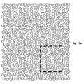
さらにまた、凹凸パターンを形成するための下層側凹凸形成膜13a(柱状突起(凹凸))の分布を変える方法としては、図15を参照して以下に説明するように、平行移動を利用してもよい。すなわち、図15に示すように、上下左右の境界のパターンが連続した基準パターンを9個つなげて配置し、このパターンから基準パターンと同一面積の切り出し枠(点線で示す)を平行移動させながら、各場所でパターンを切り出してもよい。このような方法によれば、いずれの場所で切り出されたパターンも、上下左右の連続性が確保され、かつ、枠内のパターンは、座標が平行移動したパターンを得ることができる。
【0106】
また、図16に示すように、画素よりも大きめの基準パターンを形成しておき、切り出し領域を矢印Xおよび矢印Yで示すようにずらして、座標が平行移動したパターンを作成してもよい。この際、光透過窓8dも基準パターンに含めておけば、光透過窓8dの位置パターンが異なるパターンを得ることができる。
【0107】
その際、図16に示すように、凹凸形成膜13aが形成する凹凸と重ねるように光透過窓8dを形成してもよい。この場合には、光透過窓8dの面積を凹凸形成膜13aが形成する凹凸の面積の1.2倍から1.3倍にすることが好ましい。このように構成すると、凹凸周囲の平坦部に光透過窓8dが部分的に重なるので、光の利用効率を高めることができる。
【0108】
図16に係る方法によれば、凹凸形成膜13が形成する凹凸の大部分は、画素間で平行移動した位置関係にあるとともに、これらの凹凸と光透過窓8dとの相対位置関係が画素間で同一となる。
【0109】
また、上記形態では、ユニット内では光透過窓8dが異なる位置に形成されているとともに、ユニット内における光透過窓8dの形成位置パターンがユニット間で異なっている構成であったが、多数の画素の各々において、光透過窓の形成位置のみが相違している構成であってもよい。このように構成した場合でも、反射領域の形成位置が異なる画素が存在するので、たとえ、凹凸パターンの形態が全画素で共通であったとしても、光反射膜からの反射光の干渉を抑制することができる。
【0110】
さらに、上記形態では、ユニット内では画素毎に凹凸パターンが異なる形態をもって形成されているとともに、ユニット内における各凹凸パターンの位置がユニット間で異なっている構成であったが、多数の画素の各々に凹凸パターンが異なる形態をもって形成されている構成であってもよい。
【0111】
さらにまた、上記のいずれの形態も、画素スイッチング素子としてTFTを用いたアクティブマトリクス型の液晶装置を例に説明したが、画素スイッチング素子としてTFDを用いたアクティブマトリクス型の液晶装置、あるいはパッシブマトリクス型の液晶装置、さらには液晶以外の電気光学物質を用いた半透過・反射型電気光学装置に本発明を適用してもよい。
【0112】
[半透過・反射型電気光学装置の電子機器への適用]
このように構成した反射型、あるいは半透過・半反射型の半透過・反射型電気光学装置100は、各種の電子機器の表示部として用いることができるが、その一例を、図17、図18(A)、(B)を参照して説明する。
【0113】
図17は、本発明に係る半透過・反射型電気光学装置を表示装置として用いた電子機器の回路構成を示すブロック図である。
【0114】
図17において、電子機器は、表示情報出力源70、表示情報処理回路71、電源回路72、タイミングジェネレータ73、そして液晶装置74を有する。また、液晶装置74は、液晶表示パネル75および駆動回路76を有する。液晶装置74としては、前述した半透過・反射型電気光学装置100を用いることができる。
【0115】
表示情報出力源70は、ROM(Read Only Memory)、RAM(Random Access Memory)等といったメモリ、各種ディスク等といったストレージユニット、デジタル画像信号を同調出力する同調回路等を備え、タイミングジェネレータ73によって生成された各種のクロック信号に基づいて、所定フォーマットの画像信号等といった表示情報を表示情報処理回路71に供給する。
【0116】
表示情報処理回路71は、シリアル−パラレル変換回路や、増幅・反転回路、ローテーション回路、ガンマ補正回路、クランプ回路等といった周知の各種回路を備え、入力した表示情報の処理を実行して、その画像信号をクロック信号CLKと共に駆動回路76へ供給する。電源回路72は、各構成要素に所定の電圧を供給する。
【0117】
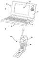
図18(A)は、本発明に係る電子機器の一実施形態であるモバイル型のパーソナルコンピュータを示している。ここに示すパーソナルコンピュータ80は、キーボード81を備えた本体部82と、液晶表示ユニット83とを有する。液晶表示ユニット83は、前述した半透過・反射型電気光学装置100を含んで構成される。
【0118】
図18(B)は、本発明に係る電子機器の他の実施形態である携帯電話機を示している。ここに示す携帯電話機90は、複数の操作ボタン91と、前述した半透過・反射型電気光学装置100からなる表示部とを有している。
【0119】
【発明の効果】
以上のとおり、本発明では、画素毎に光透過窓の形成位置が異なっているため、画素の同一位置に光透過窓が繰り返し、出現するようなことがない。それ故、光反射膜からの反射光に干渉が発生しない。
【図面の簡単な説明】
【図1】 半透過・反射型電気光学装置を対向基板の側からみたときの平面図である。
【図2】 図1のH−H′線における断面図である。
【図3】 半透過・反射型電気光学装置において、マトリクス状に配置された複数の画素に形成された各種素子、配線などの等価回路図である。
【図4】 本発明を適用した半透過・反射型電気光学装置において、TFTアレイ基板に形成された各画素の構成を示す平面図である。
【図5】 図4のA−A′線に相当する位置で切断したときの画素の断面図である。
【図6】 (A)〜(D)は、本発明を適用した半透過・反射型電気光学装置のTFTアレイ基板の製造方法を示す工程断面図である。
【図7】 (A)〜(D)は、本発明を適用した半透過・反射型電気光学装置のTFTアレイ基板の製造方法において、図6に示す工程に続いて行う各工程の工程断面図である。
【図8】 本発明を適用した半透過・反射型電気光学装置において、画素の各ユニットに対して、異なる凹凸パターンを配置し、かつ、異なる位置に光透過窓を形成する様子を示す説明図である。
【図9】 本発明を適用した半透過・反射型電気光学装置において、画素に形成する凹凸パターン、および光透過窓の形成位置の違いを示す説明図である。
【図10】 本発明を適用した半透過・反射型電気光学装置において、画素に形成する凹凸パターンの違い、および光透過窓の形成位置の違いを示す説明図である。
【図11】 本発明を適用した半透過・反射型電気光学装置において、画素に形成する凹凸パターンの違い、および光透過窓の形成位置の違いを示す説明図である。
【図12】 (A)、(B)はそれぞれ、凹凸の相対距離関係を評価するためのドロネイ三角形の説明図である。
【図13】 画素の端部で凹凸が途切れている様子を示す説明図である。
【図14】 本発明を適用した別の半透過・反射型電気光学装置において、光透過窓の形成位置の違いを示す説明図である。
【図15】 本発明を適用した電気光学装置において、平行移動により各種凹凸パターンを形成する方法を示す説明図である。
【図16】 本発明を適用した電気光学装置において、平行移動により各種凹凸パターンを形成する別の方法の説明図である。
【図17】 本発明に係る半透過・反射型電気光学装置を表示装置として用いた電子機器の回路構成を示すブロック図である。
【図18】 (A)、(B)はそれぞれ、本発明に係る半透過・反射型電気光学装置を用いた電子機器の一実施形態としてのモバイル型のパーソナルコンピュータ、および携帯電話機の説明図である。
【図19】 従来の半透過・反射型電気光学装置に用いたTFTアレイ基板の画素の平面図である。
【図20】 従来の半透過・反射型電気光学装置の画素の一部の断面図である。
【符号の説明】
1a 半導体膜、1a′ チャネル形成用領域、2 ゲート絶縁膜、3a 走査線、3b 容量線、4 第1層間絶縁膜、5 第2層間絶縁膜、6a データ線、6b ドレイン電極、7a 上層側凹凸形成膜、8a 光反射膜、8d 光透過窓、8g 凹凸パターン、9a 画素電極、10 TFTアレイ基板、13a下層側凹凸形成膜、20 対向基板、21 対向電極、30 画素スイッチング用のTFT、50 液晶、60 蓄積容量、100 半透過・反射型電気光学装置、100a 画素、100a′ 基準画素[0001]
BACKGROUND OF THE INVENTION
The present invention relates to a transflective electro-optical device in which an electro-optical material is held on a substrate, and an electronic apparatus using the same. More specifically, the present invention relates to a technology for forming a reflective surface on a substrate used in a transflective / reflective electro-optical device.
[0002]
[Prior art]
Electro-optical devices such as liquid crystal devices are used as direct-view display devices for various devices. Among such electro-optical devices, a reflective or semi-transmissive / semi-reflective TFT active matrix type liquid crystal device is arranged in a matrix on the surface of the
[0003]
In such an electro-optical device, when the directionality of the light reflected by the
[0004]
However, if the
[0005]
[Patent Document 1]
JP-A-10-123508
[0006]
[Problems to be solved by the invention]
However, even if the shape of the concavo-
[0007]
In view of the above problems, an object of the present invention is to provide a transflective electro-optical device and an electric apparatus that can effectively prevent interference of reflected light from a reflection region.
[0008]
[Means for Solving the Problems]
In order to solve the above problems, a transflective liquid crystal display device according to the present invention has a liquid crystal sandwiched between a pair of substrates,A pair of electrodes for driving the liquid crystal; Has a light reflecting filmAnd provided corresponding to the intersection of the data line and the scanning line. A transflective / reflective liquid crystal display device including a plurality of pixels, wherein the light reflecting film is provided with a light transmissive window for performing display with transmitted light,Pixel , N × mplural Consisting of pixelsConfigure the unit, SaidUnit n × mplural The pixels are different from each other in the formation position pattern of the light transmission window in the pixel,A plurality of the units, In multiple unitsAn array of the n × m pixels in which the light transmission window formation position patterns are different from each other, The plurality of units are different from each other.
[0009]
For example, when the large number of pixels are grouped into a plurality of units of n × m pixels, the arrangement of the light transmission window formation position patterns in the units differs among the units.
[0010]
In the present invention, a plurality of light transmission windows are formed in each pixel, and there are a plurality of formation position patterns of the light transmission windows in the pixel. For this reason, since there are pixels in which the formation positions of the reflection regions are different, interference of reflected light from the light reflection film can be suppressed even if the concavo-convex pattern is common to all pixels.
[0011]
In the present invention, it is preferable that the formation position pattern of the light transmission window is different for each pixel in the unit.
[0012]
In the present invention, it is preferable that all the positions where the light transmission windows are formed in the pixels having the same position in the units are different between the units.
[0013]
In the present invention, it is preferable that at least in the unit, the concavo-convex pattern has a different form (shape, size, distribution) for each pixel. Moreover, it is preferable that the arrangement | sequence of the said uneven | corrugated pattern in the said unit differs between the said units. If comprised in this way, even if the formation position of a reflection area overlaps between pixels, the uneven | corrugated pattern of the same shape does not appear repeatedly. Therefore, interference does not occur in the reflected light from the light reflecting film.
[0014]
Furthermore, if the number of pixels of a unit having a different light transmission window formation position pattern and a unit having a different concave / convex pattern form are different, the transmission window formation position pattern between the pixels even if the same unit is repeated. It is possible to reduce the probability of the appearance of pixels having the same pattern shape.
[0015]
In another aspect of the present invention, a concavo-convex forming film formed in a state where a plurality of concavo-convex formed of protrusions or holes are dispersed in each of a plurality of pixels configured in a matrix on a substrate holding an electro-optic material, A light reflecting film formed on an upper layer side of the unevenness forming film, and an uneven pattern for light scattering is formed on the surface of the light reflecting film by the unevenness forming film, and the light reflecting film In the semi-transmissive / reflective electro-optical device in which a light transmissive window for performing display by transmitted light is formed, the formation position of the light transmissive window with respect to the light reflective film is different in each of the plurality of pixels. It is characterized by being.
[0016]
In the present invention, since the formation position of the light transmission window is different for each pixel, the light transmission window does not appear repeatedly. Therefore, the light transmission window does not cause interference in the reflected light from the light reflecting film.
[0017]
In the present invention, it is preferable that the concavo-convex pattern is formed in a different form (shape, size, distribution) in each of the plurality of pixels. If comprised in this way, the same uneven | corrugated pattern will not appear repeatedly. Therefore, interference does not occur in the reflected light from the light reflecting film.
[0018]
In the present invention, in the uneven pattern, it is preferable that variation in shape, size, or distribution of the unevenness is controlled. With this configuration, it is possible to avoid the occurrence of luminance unevenness and glare between pixels.
[0019]
In the present invention, it is preferable that the light transmission window overlaps with a part of the unevenness formed by the unevenness forming film in a planar manner. If comprised in this way, when changing an uneven | corrugated pattern in the design stage, the formation position of a light transmissive window will also change in connection with it. Therefore, the design for changing the formation position of the light transmission window between pixels is easy.
[0020]
In this case, the area of the light transmission window is preferably 1.2 to 1.3 times the area of the unevenness formed by the unevenness forming film. That is, it is preferable to increase the light utilization efficiency by forming a light transmission window so as to overlap with the flat part around the unevenness.
[0021]
In the present invention, for example, most of the unevenness formed by the unevenness forming film is in a positional relationship of rotational movement between pixels, and the relative positional relationship between the unevenness and the light transmission window is the same between pixels. It is. For this configuration, for example, a pattern obtained by adding a light transmission window forming pattern to an unevenness forming pattern larger than one pixel is used as a reference pattern, and the reference pattern is rotated about a predetermined position. The position of the unevenness and the position of the light transmission window are determined for each pixel according to the pattern.
[0022]
In the present invention, most of the unevenness formed by the unevenness forming film is in a positional relationship translated between pixels, and the relative positional relationship between the unevenness and the light transmission window is the same between pixels. A certain configuration may be adopted. In order to configure in this way, for example, a rectangular basic pattern is prepared by adding a pattern for forming a light transmission window to a pattern for forming an unevenness in which a pattern at the left end and a right end and a pattern at the upper end and the lower end respectively have continuity, The position of the unevenness and the light transmission window is determined with respect to the pixel by a plurality of uneven patterns obtained by translating the cutout area from the basic pattern vertically and horizontally while maintaining the continuity of the pattern at the end. do it.
[0023]
In the present invention, even if the formation position pattern of the light transmission window is changed, the formation area of the light transmission window is preferably equal between the pixels.
[0024]
In the present invention, the substrate is a first substrate, a second substrate is disposed opposite to the first substrate, and the liquid crystal as the electro-optical material is held between the substrates so as to be transflective / reflective. Type electro-optical device.
[0025]
Such a transflective / reflective electro-optical device is used as a display unit of an electronic device such as a mobile phone or a mobile computer.
[0026]
DETAILED DESCRIPTION OF THE INVENTION
Embodiments of the present invention will be described with reference to the drawings.
[0027]
(Basic configuration of transflective electro-optical device)
FIG. 1 is a plan view of a transflective electro-optical device to which the present invention is applied as viewed from the side of a counter substrate together with each component, and FIG. 2 is a cross-sectional view taken along line HH ′ of FIG. FIG. 3 is an equivalent circuit diagram of various elements and wirings in a plurality of pixels formed in a matrix in the image display region of the transflective electro-optical device. Note that, in each drawing used in the description of the present embodiment, each layer and each member have different scales so that each layer and each member can be recognized on the drawing.
[0028]
1 and 2, in the transflective electro-optical device 100 (liquid crystal device) of this embodiment, the TFT array substrate 10 (first substrate) and the counter substrate 20 (second substrate) have a sealing
[0029]
Instead of forming the data line driving
[0030]
When the transflective electro-
[0031]
In the image display area of the transflective electro-
[0032]
Here, the
[0033]
In order to prevent the retained pixel signals S1, S2,... Sn from leaking, a
[0034]
(Configuration of TFT array substrate)
FIG. 4 is a plan view of a plurality of pixel groups adjacent to each other on the TFT array substrate used in the transflective electro-optical device of this embodiment. FIG. 5 is a cross-sectional view of a part of the pixels of the transflective electro-optical device cut at a position corresponding to the line AA ′ in FIG.
[0035]
In FIG. 4,
[0036]
In each of the
[0037]
As shown in FIG. 5, the cross section taken along the line AA ′ of the
[0038]
On the surface side of the
[0039]
On the upper layer of the second
[0040]
Here, the
[0041]
A
[0042]
An
[0043]
Further, the extension portion 1f (lower electrode) extending from the high-concentration drain region 1e has a capacitance in the same layer as the
[0044]
The
[0045]
In this embodiment, a single gate structure is employed in which only one gate electrode (scanning
[0046]
(Structure of
4 and 5, in the
[0047]
In constructing such a concavo-
[0048]
In addition, after forming the lower layer side
[0049]
Here, the columnar protrusions that form irregularities in the lower-layer-side
[0050]
As described above, the shape, size, and distribution of the
[0051]
(Configuration of counter substrate)
In FIG. 5, in the
[0052]
(TFT manufacturing method)
A method for manufacturing the
[0053]
FIGS. 6 and 7 are process cross-sectional views showing the manufacturing method of the
[0054]
In manufacturing the
[0055]
In manufacturing the
[0056]
Next, after thickly applying the organic
[0057]
Next, the exposed
[0058]
Next, as shown in FIG. 6C, after applying perhydropolysilazane or a composition containing the same to the surface side of the second
[0059]
Perhydropolysilazane is a kind of inorganic polysilazane, and is a coating type coating material that is converted into a silicon oxide film by baking in the air. For example, polysilazane manufactured by Tonen Corporation is-(SiH2 It is an inorganic polymer having NH)-as a unit, and is soluble in an organic solvent such as xylene. Accordingly, when this inorganic polymer organic solvent solution (for example, 20% xylene solution) is applied as a coating solution by a spin coating method (for example, 2000 rpm, 20 seconds) and then baked in the atmosphere at a temperature of 450 ° C., moisture and A dense amorphous silicon oxide film equivalent to or better than a silicon oxide film formed by a CVD method by reacting with oxygen can be obtained.
[0060]
Here, since the upper layer side
[0061]
In addition, when forming the uneven |
[0062]
Next, as shown in FIG. 7A, after a
[0063]
Next, the
[0064]
Further, in this step, the
[0065]
Next, as shown in FIG. 7C, an
[0066]
Next, the
[0067]
Thereafter, as shown in FIG. 5, a polyimide film (alignment film 12) is formed on the surface side of the
[0068]
As a result, the
[0069]
(Relationship between the
FIG. 8 shows that when a large number of pixels are grouped into a plurality of units on the TFT array substrate, at least in the unit, the concavo-convex pattern is formed differently for each pixel. It is explanatory drawing which shows a mode that the position of an uneven | corrugated pattern differs between units. FIGS. 9, 10, and 11 are explanatory views of the uneven pattern attached to the TFT array substrate of the transflective electro-optical device according to the present embodiment. FIG. 12 is an explanatory diagram of Delaunay triangles for evaluating the relative distance relationship between the projections and depressions.
[0070]
In the transflective / reflective electro-
[0071]
The
[0072]
Further, in this embodiment, the lower layer side
[0073]
However, if the concavo-
[0074]
Therefore, in this embodiment, first, as shown in FIG. 8, a large number of
[0075]
That is, when forming the lower-side
[0076]
Here, a plurality of types of projections and depressions having different planar sizes are formed, but they are shown in the same size in FIGS.
[0077]
Further, the positions of the concave and convex patterns A to L in the
[0078]
In addition, the
[0079]
In forming such a plurality of types of concavo-convex patterns, when designing the
[0080]
Here, the rotation center O1 is set in the pixel region. In such a case, it is preferable to set the rotation center at a position shifted from the center of the lower-layer uneven forming
[0081]
Further, when designing the
[0082]
Further, when designing the
[0083]
In the transflective / reflective electro-
[0084]
In this embodiment, when the
[0085]
Further, in this embodiment, the lower layer side
[0086]
Further, the ratio of the unevenness in which the slope of the slope formed on the side surface of the lower-side
[0087]
Furthermore, the variation in the area where the lower side
[0088]
Furthermore, as shown in FIG. 12A, when a Delaunay diagram is drawn from the position coordinates of the centers of the plurality of lower side
[0089]
Therefore, the variation in the reflected luminance when viewed from a direction inclined by 10 to 30 degrees from the normal direction with respect to the
[0090]
Here, when the planar shape of the lower-side
[0091]
As shown in FIG. 13, when the lower layer side
[0092]
(Relationship between
Further, in the present embodiment, as shown in FIG. 4, the formation position of the
[0093]
In other words, when designing the formation position pattern of the
[0094]
Further, the
[0095]
In forming such a plurality of types of formation position patterns, in this embodiment, for example, the
[0096]
Further, the
[0097]
Further, the
[0098]
As described above, in the semi-transmissive / reflective electro-
[0099]
In this embodiment, when the
[0100]
In addition, even if the formation positions of the reflection regions partially overlap between the
[0101]
Furthermore, the relative positions of the
[0102]
In addition, when rotating a concavo-convex pattern as shown in FIGS. 9-11, when the
[0103]
[Other embodiments]
In the above embodiment, the
[0104]
In the above embodiment, the lower side
[0105]
Furthermore, as a method of changing the distribution of the lower layer side
[0106]
In addition, as shown in FIG. 16, a reference pattern larger than the pixel may be formed, and the cutout area may be shifted as indicated by arrows X and Y to create a pattern whose coordinates are moved in parallel. At this time, if the
[0107]
At this time, as shown in FIG. 16, the
[0108]
According to the method according to FIG. 16, most of the unevenness formed by the
[0109]
In the above embodiment, the
[0110]
Furthermore, in the above embodiment, the concave / convex pattern is formed differently for each pixel in the unit, and the position of each concave / convex pattern in the unit is different between units. The concavo-convex pattern may be formed in a different form.
[0111]
Furthermore, in any of the above embodiments, an active matrix liquid crystal device using TFT as a pixel switching element has been described as an example. However, an active matrix liquid crystal device using TFD as a pixel switching element, or a passive matrix type liquid crystal device. The present invention may be applied to a liquid crystal device, and a transflective electro-optical device using an electro-optical material other than liquid crystal.
[0112]
[Application of transflective electro-optical device to electronic equipment]
The reflective or semi-transmissive / semi-reflective semi-transmissive / reflective electro-
[0113]
FIG. 17 is a block diagram showing a circuit configuration of an electronic apparatus using the transflective electro-optical device according to the present invention as a display device.
[0114]
In FIG. 17, the electronic device includes a display
[0115]
The display
[0116]
The display
[0117]
FIG. 18A shows a mobile personal computer which is an embodiment of an electronic apparatus according to the invention. The
[0118]
FIG. 18B shows a mobile phone which is another embodiment of the electronic apparatus according to the invention. A
[0119]
【The invention's effect】
As described above, in the present invention, since the light transmission window is formed at different positions for each pixel, the light transmission window does not appear repeatedly at the same position in the pixel. Therefore, interference does not occur in the reflected light from the light reflecting film.
[Brief description of the drawings]
FIG. 1 is a plan view of a transflective electro-optical device as viewed from the counter substrate side.
FIG. 2 is a cross-sectional view taken along the line HH ′ of FIG.
FIG. 3 is an equivalent circuit diagram of various elements and wirings formed in a plurality of pixels arranged in a matrix in a transflective electro-optical device.
FIG. 4 is a plan view showing a configuration of each pixel formed on a TFT array substrate in a transflective electro-optical device to which the present invention is applied.
5 is a cross-sectional view of a pixel when cut at a position corresponding to the line AA ′ in FIG. 4;
6A to 6D are process cross-sectional views illustrating a method of manufacturing a TFT array substrate of a transflective electro-optical device to which the present invention is applied.
FIGS. 7A to 7D are process cross-sectional views of processes performed subsequent to the process shown in FIG. 6 in the method of manufacturing a TFT array substrate of a transflective electro-optical device to which the present invention is applied. It is.
FIG. 8 is an explanatory diagram showing a state in which different concavo-convex patterns are arranged for each unit of a pixel and light transmission windows are formed at different positions in a transflective electro-optical device to which the present invention is applied. It is.
FIG. 9 is an explanatory diagram illustrating a difference in the formation pattern of a concavo-convex pattern formed on a pixel and a light transmission window in a transflective electro-optical device to which the invention is applied.
FIG. 10 is an explanatory diagram showing a difference in uneven pattern formed in a pixel and a difference in formation position of a light transmission window in a transflective electro-optical device to which the invention is applied.
FIG. 11 is an explanatory diagram showing a difference in uneven pattern formed on a pixel and a difference in formation position of a light transmission window in a transflective / reflective electro-optical device to which the invention is applied.
FIGS. 12A and 12B are explanatory diagrams of Delaunay triangles for evaluating the relative distance relationship between the projections and depressions, respectively.
FIG. 13 is an explanatory diagram illustrating a state in which unevenness is interrupted at an end portion of a pixel.
FIG. 14 is an explanatory diagram showing a difference in the formation position of a light transmission window in another transflective electro-optical device to which the present invention is applied.
FIG. 15 is an explanatory diagram illustrating a method for forming various uneven patterns by parallel movement in an electro-optical device to which the invention is applied.
FIG. 16 is an explanatory diagram of another method for forming various uneven patterns by parallel movement in the electro-optical device to which the invention is applied.
FIG. 17 is a block diagram illustrating a circuit configuration of an electronic apparatus using the transflective electro-optical device according to the present invention as a display device.
FIGS. 18A and 18B are explanatory views of a mobile personal computer and a mobile phone as an embodiment of an electronic apparatus using the transflective electro-optical device according to the present invention, respectively. is there.
FIG. 19 is a plan view of a pixel of a TFT array substrate used in a conventional transflective / reflective electro-optical device.
FIG. 20 is a cross-sectional view of a part of a pixel of a conventional transflective electro-optical device.
[Explanation of symbols]
1a Semiconductor film, 1a 'channel forming region, 2 gate insulating film, 3a scanning line, 3b capacitance line, 4th first interlayer insulating film, 5th second interlayer insulating film, 6a data line, 6b drain electrode, 7a upper layer side unevenness Formation film, 8a Light reflection film, 8d Light transmission window, 8g Uneven pattern, 9a Pixel electrode, 10 TFT array substrate, 13a Lower layer uneven formation film, 20 Counter substrate, 21 Counter electrode, 30 Pixel switching TFT, 50
Claims (11)
Translated fromJapanese前記光反射膜には透過光による表示を行うための光透過窓が設けられ、
前記画素は、n×m個の複数の画素からなるユニットを構成し、
前記ユニットのn×m個の複数の画素は、当該画素内における前記光透過窓の形成位置パターンが互いに異なり、
前記ユニットを複数有し、前記複数のユニットにおける前記光透過窓の形成位置パターンが互いに異なる前記n×m個の画素の配列が、前記複数のユニット間で異なっていることを特徴とする半透過・反射型液晶表示装置。Liquid crystal is sandwiched between a pair of substrates,the semi-transmissive reflective liquid crystal having a plurality ofpixels provided to correspond to intersections of the data lines and the scan lines and having apair of electrodes and a light reflecting filmfor driving the liquid crystal A display device,
The light reflection film is provided with a light transmission window for performing display with transmitted light,
Thepixelconstitutes a unit composed of aplurality of n × m pixels,
N × m pieces ofthe plurality of pixelsof theunit is different from the formation position pattern of the light transmission window within the pixel is from each other,
A plurality of the units, andthe arrangement of the n × m pixels having different light transmission window formation position patterns in the plurality of units is different among the plurality of units. -Reflective liquid crystal display device.
前記凹凸と前記光透過窓との相対位置関係は画素間で同一であることを特徴とする半透過・反射型液晶表示装置。5. The concave / convex pattern formed by the concave / convex forming film according to claim 3 or 4, wherein the concave / convex pattern has the same area as the reference pattern from a pattern formed by connecting a plurality of reference patterns in the upper / lower / left / right boundary pattern. a pattern cut out while translating the clippingframe,
The transflective liquid crystal display device characterized in that the relative positional relationship between the unevenness and the light transmission window is the same between pixels.
Priority Applications (1)
| Application Number | Priority Date | Filing Date | Title |
|---|---|---|---|
| JP2003068321AJP4513269B2 (en) | 2003-03-13 | 2003-03-13 | Transflective liquid crystal display device and electronic equipment |
Applications Claiming Priority (1)
| Application Number | Priority Date | Filing Date | Title |
|---|---|---|---|
| JP2003068321AJP4513269B2 (en) | 2003-03-13 | 2003-03-13 | Transflective liquid crystal display device and electronic equipment |
Publications (2)
| Publication Number | Publication Date |
|---|---|
| JP2004279560A JP2004279560A (en) | 2004-10-07 |
| JP4513269B2true JP4513269B2 (en) | 2010-07-28 |
Family
ID=33285696
Family Applications (1)
| Application Number | Title | Priority Date | Filing Date |
|---|---|---|---|
| JP2003068321AExpired - Fee RelatedJP4513269B2 (en) | 2003-03-13 | 2003-03-13 | Transflective liquid crystal display device and electronic equipment |
Country Status (1)
| Country | Link |
|---|---|
| JP (1) | JP4513269B2 (en) |
Family Cites Families (3)
| Publication number | Priority date | Publication date | Assignee | Title |
|---|---|---|---|---|
| JP2001075091A (en)* | 1999-07-07 | 2001-03-23 | Matsushita Electric Ind Co Ltd | Transflective liquid crystal display |
| JP2002243923A (en)* | 2001-02-14 | 2002-08-28 | Matsushita Electric Ind Co Ltd | Reflection plate and reflective liquid crystal display panel |
| JP2003241184A (en)* | 2002-02-15 | 2003-08-27 | Matsushita Electric Ind Co Ltd | Liquid crystal display device and transflective liquid crystal display device |
- 2003
- 2003-03-13JPJP2003068321Apatent/JP4513269B2/ennot_activeExpired - Fee Related
Also Published As
| Publication number | Publication date |
|---|---|
| JP2004279560A (en) | 2004-10-07 |
Similar Documents
| Publication | Publication Date | Title |
|---|---|---|
| JP3714244B2 (en) | Transflective / reflective electro-optical device manufacturing method, transflective / reflective electro-optical device, and electronic apparatus | |
| KR100461287B1 (en) | Electrical optics devices | |
| KR100674291B1 (en) | Electro-optical devices and electronic devices | |
| KR100514507B1 (en) | Electrooptic device and production method therefor | |
| US20040105054A1 (en) | Electro-optical device and electronic apparatus | |
| JP3722116B2 (en) | Reflective electro-optical device and electronic apparatus | |
| JP4154880B2 (en) | Electro-optical device and manufacturing method thereof | |
| JP3951694B2 (en) | Transflective / reflective electro-optical device, electronic apparatus, and method of manufacturing transflective / reflective electro-optical device | |
| JP4035992B2 (en) | Electro-optical device, electronic apparatus, and method of manufacturing electro-optical device | |
| JP3858863B2 (en) | Electro-optical device and electronic apparatus | |
| US7157739B2 (en) | Active matrix type electro-optical device with patterns of contact hole formation-positions and electronic apparatus | |
| JP4513269B2 (en) | Transflective liquid crystal display device and electronic equipment | |
| JP4400027B2 (en) | Transflective / reflective electro-optical device and electronic apparatus using the same | |
| JP3979077B2 (en) | Electro-optical device and electronic apparatus | |
| JP4371104B2 (en) | Electro-optical device and electronic apparatus | |
| KR101000442B1 (en) | Reflective-transmissive polysilicon liquid crystal display and manufacturing method thereof | |
| JP2003029298A (en) | Thin-film semiconductor device, electro-optical device, electronic equipment, thin-film semiconductor device, and method of manufacturing electro-optical device | |
| JP2003005173A (en) | Electro-optical devices and electronic equipment | |
| JP2004334155A (en) | Electro-optical devices and electronic equipment | |
| JP2003195285A (en) | Reflective electro-optical device, electronic apparatus, and method of manufacturing reflective electro-optical device | |
| JP3932844B2 (en) | Electro-optical device and manufacturing method thereof | |
| JP2003076300A (en) | Electro-optical device and method of manufacturing the same | |
| JP2004045756A (en) | Transflective / reflective electro-optical device and electronic apparatus using the same | |
| JP2003287773A (en) | Reflective electro-optical device and electronic equipment | |
| JP2003262863A (en) | Transflective / reflective electro-optical device, electronic apparatus, and method of manufacturing transflective / reflective electro-optical device |
Legal Events
| Date | Code | Title | Description |
|---|---|---|---|
| A621 | Written request for application examination | Free format text:JAPANESE INTERMEDIATE CODE: A621 Effective date:20051129 | |
| RD04 | Notification of resignation of power of attorney | Free format text:JAPANESE INTERMEDIATE CODE: A7424 Effective date:20070402 | |
| A977 | Report on retrieval | Free format text:JAPANESE INTERMEDIATE CODE: A971007 Effective date:20080516 | |
| A131 | Notification of reasons for refusal | Free format text:JAPANESE INTERMEDIATE CODE: A131 Effective date:20080527 | |
| A521 | Request for written amendment filed | Free format text:JAPANESE INTERMEDIATE CODE: A523 Effective date:20080725 | |
| A131 | Notification of reasons for refusal | Free format text:JAPANESE INTERMEDIATE CODE: A131 Effective date:20090811 | |
| A521 | Request for written amendment filed | Free format text:JAPANESE INTERMEDIATE CODE: A523 Effective date:20091009 | |
| A02 | Decision of refusal | Free format text:JAPANESE INTERMEDIATE CODE: A02 Effective date:20091215 | |
| A521 | Request for written amendment filed | Free format text:JAPANESE INTERMEDIATE CODE: A523 Effective date:20100312 | |
| A911 | Transfer to examiner for re-examination before appeal (zenchi) | Free format text:JAPANESE INTERMEDIATE CODE: A911 Effective date:20100325 | |
| TRDD | Decision of grant or rejection written | ||
| A01 | Written decision to grant a patent or to grant a registration (utility model) | Free format text:JAPANESE INTERMEDIATE CODE: A01 Effective date:20100420 | |
| A01 | Written decision to grant a patent or to grant a registration (utility model) | Free format text:JAPANESE INTERMEDIATE CODE: A01 | |
| A61 | First payment of annual fees (during grant procedure) | Free format text:JAPANESE INTERMEDIATE CODE: A61 Effective date:20100503 | |
| R150 | Certificate of patent or registration of utility model | Free format text:JAPANESE INTERMEDIATE CODE: R150 | |
| FPAY | Renewal fee payment (event date is renewal date of database) | Free format text:PAYMENT UNTIL: 20130521 Year of fee payment:3 | |
| FPAY | Renewal fee payment (event date is renewal date of database) | Free format text:PAYMENT UNTIL: 20140521 Year of fee payment:4 | |
| LAPS | Cancellation because of no payment of annual fees |