JP4509573B2 - Semiconductor substrate, semiconductor chip, and semiconductor device manufacturing method - Google Patents
Semiconductor substrate, semiconductor chip, and semiconductor device manufacturing methodDownload PDFInfo
- Publication number
- JP4509573B2 JP4509573B2JP2003574373AJP2003574373AJP4509573B2JP 4509573 B2JP4509573 B2JP 4509573B2JP 2003574373 AJP2003574373 AJP 2003574373AJP 2003574373 AJP2003574373 AJP 2003574373AJP 4509573 B2JP4509573 B2JP 4509573B2
- Authority
- JP
- Japan
- Prior art keywords
- semiconductor substrate
- region
- cutting
- semiconductor
- laser beam
- Prior art date
- Legal status (The legal status is an assumption and is not a legal conclusion. Google has not performed a legal analysis and makes no representation as to the accuracy of the status listed.)
- Expired - Lifetime
Links
Images


Classifications
- B—PERFORMING OPERATIONS; TRANSPORTING
- B28—WORKING CEMENT, CLAY, OR STONE
- B28D—WORKING STONE OR STONE-LIKE MATERIALS
- B28D5/00—Fine working of gems, jewels, crystals, e.g. of semiconductor material; apparatus or devices therefor
- B28D5/0005—Fine working of gems, jewels, crystals, e.g. of semiconductor material; apparatus or devices therefor by breaking, e.g. dicing
- B28D5/0011—Fine working of gems, jewels, crystals, e.g. of semiconductor material; apparatus or devices therefor by breaking, e.g. dicing with preliminary treatment, e.g. weakening by scoring
- B—PERFORMING OPERATIONS; TRANSPORTING
- B23—MACHINE TOOLS; METAL-WORKING NOT OTHERWISE PROVIDED FOR
- B23K—SOLDERING OR UNSOLDERING; WELDING; CLADDING OR PLATING BY SOLDERING OR WELDING; CUTTING BY APPLYING HEAT LOCALLY, e.g. FLAME CUTTING; WORKING BY LASER BEAM
- B23K26/00—Working by laser beam, e.g. welding, cutting or boring
- B23K26/36—Removing material
- B23K26/40—Removing material taking account of the properties of the material involved
- B—PERFORMING OPERATIONS; TRANSPORTING
- B23—MACHINE TOOLS; METAL-WORKING NOT OTHERWISE PROVIDED FOR
- B23K—SOLDERING OR UNSOLDERING; WELDING; CLADDING OR PLATING BY SOLDERING OR WELDING; CUTTING BY APPLYING HEAT LOCALLY, e.g. FLAME CUTTING; WORKING BY LASER BEAM
- B23K26/00—Working by laser beam, e.g. welding, cutting or boring
- B23K26/50—Working by transmitting the laser beam through or within the workpiece
- B23K26/53—Working by transmitting the laser beam through or within the workpiece for modifying or reforming the material inside the workpiece, e.g. for producing break initiation cracks
- B—PERFORMING OPERATIONS; TRANSPORTING
- B23—MACHINE TOOLS; METAL-WORKING NOT OTHERWISE PROVIDED FOR
- B23K—SOLDERING OR UNSOLDERING; WELDING; CLADDING OR PLATING BY SOLDERING OR WELDING; CUTTING BY APPLYING HEAT LOCALLY, e.g. FLAME CUTTING; WORKING BY LASER BEAM
- B23K2101/00—Articles made by soldering, welding or cutting
- B23K2101/36—Electric or electronic devices
- B23K2101/40—Semiconductor devices
- B—PERFORMING OPERATIONS; TRANSPORTING
- B23—MACHINE TOOLS; METAL-WORKING NOT OTHERWISE PROVIDED FOR
- B23K—SOLDERING OR UNSOLDERING; WELDING; CLADDING OR PLATING BY SOLDERING OR WELDING; CUTTING BY APPLYING HEAT LOCALLY, e.g. FLAME CUTTING; WORKING BY LASER BEAM
- B23K2103/00—Materials to be soldered, welded or cut
- B23K2103/50—Inorganic material, e.g. metals, not provided for in B23K2103/02 – B23K2103/26
Landscapes
- Engineering & Computer Science (AREA)
- Mechanical Engineering (AREA)
- Physics & Mathematics (AREA)
- Optics & Photonics (AREA)
- Plasma & Fusion (AREA)
- Chemical & Material Sciences (AREA)
- Chemical Kinetics & Catalysis (AREA)
- General Chemical & Material Sciences (AREA)
- Oil, Petroleum & Natural Gas (AREA)
- Laser Beam Processing (AREA)
Description
Translated fromJapanese技術分野
本発明は、半導体デバイスを製造するために好適に用いられる半導体基板、半導体チップ、及び半導体デバイスの製造方法に関する。
背景技術
半導体デバイスの製造工程においては、シリコンウェハ等の半導体基板上に複数の機能素子を形成した後に、ダイヤモンドブレードにより半導体基板を機能素子毎に切断し(切削加工)、半導体チップを得るのが一般的である。
また、上記ダイヤモンドブレードによる切断に代えて、半導体基板に対して吸収性を有するレーザ光を半導体基板に照射し、加熱溶融により半導体基板を切断することもある(加熱溶融加工)。
発明の開示
しかしながら、上述した切削加工や加熱溶融加工による半導体基板の切断は、半導体基板上に機能素子を形成した後に行われるため、例えば切断時に発生する熱を原因として機能素子が破壊されるおそれがある。
そこで、本発明は、このような事情に鑑みてなされたものであり、半導体デバイスの製造工程における切断によって機能素子が破壊されるのを防止することのできる半導体基板、半導体チップ、及び半導体デバイスの製造方法を提供することを目的とする。
上記目的を達成するために、本発明に係る半導体基板は、レーザ光の照射により当該レーザ光の集光点の位置で形成される多光子吸収による改質領域によって、切断起点領域が内部に形成されていることを特徴とする。
この半導体基板よれば、レーザ光の照射により当該レーザ光の集光点の位置で形成される多光子吸収による改質領域が、半導体基板の内部に形成されている。すなわち、この改質領域は、レーザ光の集光点が半導体基板の内部に合わされ、当該集光点の位置で多光子吸収という現象が発生することで、半導体基板の内部に形成される。この多光子吸収を発生し得るレーザ光の照射においては、半導体基板の表面ではレーザ光がほとんど吸収されないため、半導体基板の表面が溶融することはない。したがって、半導体デバイスの製造工程において、従来通り半導体基板の表面に機能素子を形成することができる。さらに、この半導体基板によれば、改質領域によって切断起点領域が半導体基板の内部に形成されている。半導体基板の内部に改質領域が形成されていると、改質領域を起点として比較的小さな力で半導体基板に割れが発生するため、切断起点領域に沿って高い精度で半導体基板を割って切断することができる。したがって、半導体デバイスの製造工程において、従来のような機能素子形成後の切削加工や加熱溶融加工が不要となり、半導体基板の切断による機能素子の破壊を防止することができる。
ここで、集光点とは、レーザ光が集光した箇所のことである。また、機能素子とは、フォトダイオード等の受光素子やレーザダイオード等の発光素子、或いは回路として形成された回路素子等を意味する。さらに、切断起点領域とは、半導体基板が切断される際に切断の起点となる領域を意味する。したがって、切断起点領域は、半導体基板において切断が予定される切断予定部である。そして、切断起点領域は、改質領域が連続的に形成されることで形成される場合もあるし、改質領域が断続的に形成されることで形成される場合もある。
また、本発明に係る半導体基板は、集光点におけるピークパワー密度が1×10⁸(W/cm2)以上で且つパルス幅が1μs以下の条件でのレーザ光の照射により当該レーザ光の集光点の位置で形成される溶融処理領域を含む改質領域によって、切断起点領域が内部に形成されていることを特徴とする。
この半導体基板によれば、集光点におけるピークパワー密度が1×10⁸(W/cm2)以上で且つパルス幅が1μs以下の条件でのレーザ光の照射により当該レーザ光の集光点の位置で形成される溶融処理領域を含む改質領域が、半導体基板の内部に形成されている。すなわち、この溶融処理領域は、レーザ光の集光点が半導体基板の内部に合わされ、当該集光点の位置で多光子吸収という現象が発生し局所的に加熱されることで、半導体基板の内部に形成される。この溶融処理領域は上述した改質領域の一例であるので、この半導体基板によっても、半導体デバイスの製造工程において、半導体基板の表面に機能素子を形成することができ、且つ機能素子形成後における半導体基板の切断による機能素子の破壊を防止することができる。
また、本発明に係る半導体基板は、レーザ光の照射により当該レーザ光の集光点の位置で形成される改質領域によって、切断起点領域が内部に形成されていることを特徴とする。そして、この改質領域は、溶融処理した領域である場合もある。
この半導体基板によれば、上述した本発明に係る半導体基板と同様の理由により、半導体デバイスの製造工程において、半導体基板の表面に機能素子を形成することができ、且つ機能素子形成後における半導体基板の切断による機能素子の破壊を防止することができる。ただし、改質領域の形成は、多光子吸収が原因となる場合もあるし、他が原因となる場合もある。
また、本発明に係る半導体基板は、外縁に沿った外縁部を有し、外縁部の内側部分の内部には改質領域によって切断起点領域が形成されていることを特徴とする。
この半導体基板によれば、上述した本発明に係る半導体基板と同様の理由により、半導体デバイスの製造工程において、半導体基板の表面に機能素子を形成することができ、且つ機能素子形成後における半導体基板の切断による機能素子の破壊を防止することができる。しかも、半導体基板における外縁部の内側部分の内部に切断起点領域を形成することで、半導体基板の搬送工程や機能素子形成のための加熱工程等において半導体基板の不測の切断を防止することが可能になる。
このとき、切断起点領域は格子状に形成されており、切断起点領域により仕切られた区画部のうち、外縁部側に位置する区画部の角部分においては、切断起点領域が交差して形成されていることが好ましい。これにより、外縁部側に位置する区画部の角部分においても、当該区画部の他の部分と同様に切断起点領域の形成が確実且つ良好なものとなり、半導体基板を切断した際に当該区画部に対応する半導体チップにチッピングやクラッキングが発生するのを防止することが可能になる。ここで、格子状とは、直交する2つの方向に延在する切断起点領域が交差する場合に限らず、互いに異なる2つの方向に延在する切断起点領域が交差する場合を意味する。また、交差とは、互いに異なる2つの方向に沿った切断起点領域が直接交わる場合に限らず、互いに異なる2つの方向に沿った切断起点領域が立体的に交わる場合(すなわち、ねじれの関係にある場合)をも含む意味である。
また、半導体基板の表面には、半導体基板の内部に形成された切断起点領域の位置を識別するための識別マークが設けられていることが好ましい。切断起点領域は半導体基板の内部に形成されているが、切断起点領域の位置を識別するための識別マークが半導体基板の表面に設けられているため、半導体デバイスの製造工程において、半導体基板の内部に形成された切断起点領域の位置を認識マークに基づいて把握し、機能素子のパターンニングや半導体基板の切断等を行うことができる。
上記目的を達成するために、本発明に係る半導体チップは、半導体基板の内部に集光点を合わせてレーザ光を照射することにより、半導体基板の内部に多光子吸収による改質領域を形成し、当該改質領域を切断起点領域として半導体基板の切断をすることで形成され、切断による切断面に改質領域を有していることを特徴とする。
この半導体チップによれば、改質領域により切断面が保護されるため、切断面におけるチッピングやクラッキングの発生を防止することができる。さらに、半導体チップの周縁部が切断面により囲まれている場合には、半導体チップの周縁部が改質領域により囲まれることとなり、これにより、半導体チップの抗折強度を向上させることができる。
また、本発明に係る半導体チップは、半導体基板の内部に集光点を合わせて、集光点におけるピークパワー密度が1×10⁸(W/cm2)以上で且つパルス幅が1μs以下の条件でレーザ光を照射することにより、半導体基板の内部に溶融処理領域を含む改質領域を形成し、当該溶融処理領域を含む改質領域を切断起点領域として半導体基板の切断をすることで形成され、切断による切断面に、溶融処理領域を含む改質領域を有していることを特徴とする。
この半導体チップにおける溶融処理領域は上述した改質領域の一例であるので、この半導体チップによっても、切断面におけるチッピングやクラッキングの発生を防止することができると共に、半導体チップの周縁部が切断面により囲まれている場合には、半導体チップの抗折強度を向上させることができる。
また、本発明に係る半導体チップは、半導体基板の内部に集光点を合わせてレーザ光を照射することにより、半導体基板の内部に改質領域を形成し、当該改質領域を切断起点領域として半導体基板の切断をすることで形成され、切断による切断面に改質領域を有していることを特徴とする。そして、この改質領域は、溶融処理した領域である場合もある。
この半導体チップによれば、上述した本発明に係る半導体チップと同様の理由により、切断面におけるチッピングやクラッキングの発生を防止することができると共に、半導体チップの周縁部が切断面により囲まれている場合には、半導体チップの抗折強度を向上させることができる。ただし、改質領域の形成は、多光子吸収が原因となる場合もあるし、他が原因となる場合もある。
また、本発明に係る半導体チップは、溶融処理領域を含む改質領域が端面に形成されていることを特徴とする。
この半導体チップによれば、半導体基板の切断による切断面等の端面におけるチッピングやクラッキングの発生を防止することができると共に、半導体チップの周縁部を改質領域で囲めば、半導体チップの抗折強度を向上させることができる。
以上により、本発明に係る半導体デバイスの製造方法は、半導体基板の内部に集光点を合わせてレーザ光を照射し、半導体基板の内部に多光子吸収による改質領域を形成し、この改質領域によって、半導体基板の切断予定ラインに沿って半導体基板のレーザ光入射面から所定距離内側に切断起点領域を形成する工程と、切断起点領域を形成する工程後、半導体基板に機能素子を形成する工程と、機能素子を形成する工程後、切断起点領域に沿って半導体基板を切断する工程とを備える構成を採ることができる。そして、この改質領域は、溶融処理した領域である場合もある。
また、本発明に係る半導体デバイスの製造方法は、半導体基板の内部に集光点を合わせてレーザ光を照射し、半導体基板の内部に改質領域を形成し、この改質領域によって、半導体基板の切断予定ラインに沿って半導体基板のレーザ光入射面から所定距離内側に切断起点領域を形成する工程と、切断起点領域を形成する工程後、半導体基板に機能素子を形成する工程と、機能素子を形成する工程後、切断起点領域に沿って半導体基板を切断する工程とを備える構成を採ることができる。そして、この改質領域は、溶融処理した領域である場合もある。
発明を実施するための最良の形態
以下、図面と共に本発明の好適な実施形態について詳細に説明する。本実施形態に係る半導体基板及び半導体チップを構成するに際しては、半導体基板の内部に集光点を合わせてレーザ光を照射し、半導体基板の内部に多光子吸収による改質領域を形成する、というレーザ加工方法を使用する。そこで、このレーザ加工方法、特に多光子吸収について最初に説明する。
材料の吸収のバンドギャップEGよりも光子のエネルギーhνが小さいと光学的に透明となる。よって、材料に吸収が生じる条件はhν>EGである。しかし、光学的に透明でも、レーザ光の強度を非常に大きくするとnhν>EGの条件(n=2,3,4,・・・)で材料に吸収が生じる。この現象を多光子吸収という。パルス波の場合、レーザ光の強度はレーザ光の集光点のピークパワー密度(W/cm2)で決まり、例えばピークパワー密度が1×108(W/cm2)以上の条件で多光子吸収が生じる。ピークパワー密度は、(集光点におけるレーザ光の1パルス当たりのエネルギー)÷(レーザ光のビームスポット断面積×パルス幅)により求められる。また、連続波の場合、レーザ光の強度はレーザ光の集光点の電界強度(W/cm2)で決まる。
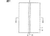
このような多光子吸収を利用する本実施形態に係るレーザ加工の原理について、図1〜図6を参照して説明する。図1はレーザ加工中の半導体基板1の平面図であり、図2は図1に示す半導体基板1のII−II線に沿った断面図であり、図3はレーザ加工後の半導体基板1の平面図であり、図4は図3に示す半導体基板1のIV−IV線に沿った断面図であり、図5は図3に示す半導体基板1のV−V線に沿った断面図であり、図6は切断された半導体基板1の平面図である。 図1及び図2に示すように、半導体基板1の表面3には、半導体基板1を切断すべき所望の切断予定ライン5がある。切断予定ライン5は直線状に延びた仮想線である(半導体基板1に実際に線を引いて切断予定ライン5としてもよい)。本実施形態に係るレーザ加工は、多光子吸収が生じる条件で半導体基板1の内部に集光点Pを合わせてレーザ光Lを半導体基板1に照射して改質領域7を形成する。なお、集光点とはレーザ光Lが集光した箇所のことである。
レーザ光Lを切断予定ライン5に沿って(すなわち矢印A方向に沿って)相対的に移動させることにより、集光点Pを切断予定ライン5に沿って移動させる。これにより、図3〜図5に示すように改質領域7が切断予定ライン5に沿って半導体基板1の内部にのみ形成され、この改質領域7でもって切断起点領域(切断予定部)9が形成される。本実施形態に係るレーザ加工方法は、半導体基板1がレーザ光Lを吸収することにより半導体基板1を発熱させて改質領域7を形成するのではない。半導体基板1にレーザ光Lを透過させ半導体基板1の内部に多光子吸収を発生させて改質領域7を形成している。よって、半導体基板1の表面3ではレーザ光Lがほとんど吸収されないので、半導体基板1の表面3が溶融することはない。
半導体基板1の切断において、切断する箇所に起点があると半導体基板1はその起点から割れるので、図6に示すように比較的小さな力で半導体基板1を切断することができる。よって、半導体基板1の表面3に不必要な割れを発生させることなく半導体基板1の切断が可能となる。
なお、切断起点領域を起点とした半導体基板の切断には、次の2通りが考えられる。1つは、切断起点領域形成後、半導体基板に人為的な力が印加されることにより、切断起点領域を起点として半導体基板が割れ、半導体基板が切断される場合である。これは、例えば半導体基板の厚さが大きい場合の切断である。人為的な力が印加されるとは、例えば、半導体基板の切断起点領域に沿って半導体基板に曲げ応力やせん断応力を加えたり、半導体基板に温度差を与えることにより熱応力を発生させたりすることである。他の1つは、切断起点領域を形成することにより、切断起点領域を起点として半導体基板の断面方向(厚さ方向)に向かって自然に割れ、結果的に半導体基板が切断される場合である。これは、例えば半導体基板の厚さが小さい場合には、1列の改質領域により切断起点領域が形成されることで可能となり、半導体基板の厚さが大きい場合には、厚さ方向に複数列形成された改質領域により切断起点領域が形成されることで可能となる。なお、この自然に割れる場合も、切断する箇所において、切断起点領域が形成されていない部位に対応する部分の表面上にまで割れが先走ることがなく、切断起点領域を形成した部位に対応する部分のみを割断することができるので、割断を制御よくすることができる。近年、シリコンウェハ等の半導体基板の厚さは薄くなる傾向にあるので、このような制御性のよい割断方法は大変有効である。
さて、本実施形態において多光子吸収により形成される改質領域としては、次に説明する溶融処理領域がある。
半導体基板の内部に集光点を合わせて、集光点における電界強度が1×10⁸(W/cm2)以上で且つパルス幅が1μs以下の条件でレーザ光を照射する。これにより半導体基板の内部は多光子吸収によって局所的に加熱される。この加熱により半導体基板の内部に溶融処理領域が形成される。溶融処理領域とは一旦溶融後再固化した領域や、まさに溶融状態の領域や、溶融状態から再固化する状態の領域であり、相変化した領域や結晶構造が変化した領域ということもできる。また、溶融処理領域とは単結晶構造、非晶質構造、多結晶構造において、ある構造が別の構造に変化した領域ということもできる。つまり、例えば、単結晶構造から非晶質構造に変化した領域、単結晶構造から多結晶構造に変化した領域、単結晶構造から非晶質構造及び多結晶構造を含む構造に変化した領域を意味する。半導体基板がシリコン単結晶構造の場合、溶融処理領域は例えば非晶質シリコン構造である。電界強度の上限値としては、例えば1×1012(W/cm2)である。パルス幅は例えば1ns〜200nsが好ましい。
本発明者は、シリコンウェハの内部で溶融処理領域が形成されることを実験により確認した。実験条件は次の通りである。
(A)半導体基板:シリコンウェハ(厚さ350μm、外径4インチ)
(B)レーザ
光源:半導体レーザ励起Nd:YAGレーザ
波長:1064nm
レーザ光スポット断面積:3.14×10⁻⁸cm2
発振形態:Qスイッチパルス
繰り返し周波数:100kHz
パルス幅:30ns
出力:20μJ/パルス
レーザ光品質:TEM00
偏光特性:直線偏光
(C)集光用レンズ
倍率:50倍
N.A.:0.55
レーザ光波長に対する透過率:60パーセント
(D)半導体基板が載置される載置台の移動速度:100mm/秒
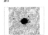
図7は、上記条件でのレーザ加工により切断されたシリコンウェハの一部における断面の写真を表した図である。シリコンウェハ11の内部に溶融処理領域13が形成されている。なお、上記条件により形成された溶融処理領域13の厚さ方向の大きさは100μm程度である。
溶融処理領域13が多光子吸収により形成されたことを説明する。図8は、レーザ光の波長とシリコン基板の内部の透過率との関係を示すグラフである。ただし、シリコン基板の表面側と裏面側それぞれの反射成分を除去し、内部のみの透過率を示している。シリコン基板の厚さtが50μm、100μm、200μm、500μm、1000μmの各々について上記関係を示した。
例えば、Nd:YAGレーザの波長である1064nmにおいて、シリコン基板の厚さが500μm以下の場合、シリコン基板の内部ではレーザ光が80%以上透過することが分かる。図7に示すシリコンウェハ11の厚さは350μmであるので、多光子吸収による溶融処理領域13はシリコンウェハの中心付近、つまり表面から175μmの部分に形成される。この場合の透過率は、厚さ200μmのシリコンウェハを参考にすると、90%以上なので、レーザ光がシリコンウェハ11の内部で吸収されるのは僅かであり、ほとんどが透過する。このことは、シリコンウェハ11の内部でレーザ光が吸収されて、溶融処理領域13がシリコンウェハ11の内部に形成(つまりレーザ光による通常の加熱で溶融処理領域が形成)されたものではなく、溶融処理領域13が多光子吸収により形成されたことを意味する。多光子吸収による溶融処理領域の形成は、例えば、溶接学会全国大会講演概要第66集(2000年4月)の第72頁〜第73頁の「ピコ秒パルスレーザによるシリコンの加工特性評価」に記載されている。
なお、シリコンウェハは、溶融処理領域でもって形成される切断起点領域を起点として断面方向に向かって割れを発生させ、その割れがシリコンウェハの表面と裏面とに到達することにより、結果的に切断される。シリコンウェハの表面と裏面に到達するこの割れは自然に成長する場合もあるし、シリコンウェハに力が印加されることにより成長する場合もある。なお、切断起点領域からシリコンウェハの表面と裏面とに割れが自然に成長する場合には、切断起点領域を形成する溶融処理領域が溶融している状態から割れが成長する場合と、切断起点領域を形成する溶融処理領域が溶融している状態から再固化する際に割れが成長する場合とのいずれもある。ただし、どちらの場合も溶融処理領域はシリコンウェハの内部のみに形成され、切断後の切断面には、図7のように内部にのみ溶融処理領域が形成されている。半導体基板の内部に溶融処理領域でもって切断起点領域を形成すると、割断時、切断起点領域ラインから外れた不必要な割れが生じにくいので、割断制御が容易となる。
以上、多光子吸収により形成される改質領域として溶融処理領域の場合を説明したが、半導体基板の結晶構造やその劈開性などを考慮して切断起点領域を次のように形成すれば、その切断起点領域を起点として、より一層小さな力で、しかも精度良く半導体基板を切断することが可能になる。
すなわち、シリコンなどのダイヤモンド構造の単結晶半導体からなる基板の場合は、(111)面(第1劈開面)や(110)面(第2劈開面)に沿った方向に切断起点領域を形成するのが好ましい。また、GaAsなどの閃亜鉛鉱型構造のIII−V族化合物半導体からなる基板の場合は、(110)面に沿った方向に切断起点領域を形成するのが好ましい。
なお、上述した切断起点領域を形成すべき方向(例えば、単結晶シリコン基板における(111)面に沿った方向)、或いは切断起点領域を形成すべき方向に直交する方向に沿って半導体基板にオリエンテーションフラットを形成すれば、そのオリエンテーションフラットを基準とすることで、切断起点領域を形成すべき方向に沿った切断起点領域を容易且つ正確に半導体基板に形成することが可能になる。
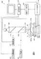
上述したレーザ加工方法に使用されるレーザ加工装置について、図9を参照して説明する。図9はレーザ加工装置100の概略構成図である。
レーザ加工装置100は、レーザ光Lを発生するレーザ光源101と、レーザ光Lの出力やパルス幅等を調節するためにレーザ光源101を制御するレーザ光源制御部102と、レーザ光Lの反射機能を有しかつレーザ光Lの光軸の向きを90°変えるように配置されたダイクロイックミラー103と、ダイクロイックミラー103で反射されたレーザ光Lを集光する集光用レンズ105と、集光用レンズ105で集光されたレーザ光Lが照射される半導体基板1が載置される載置台107と、載置台107を回転させるためのθステージ108と、載置台1、07をX軸方向に移動させるためのX軸ステージ109と、載置台107をX軸方向に直交するY軸方向に移動させるためのY軸ステージ111と、載置台107をX軸及びY軸方向に直交するZ軸方向に移動させるためのZ軸ステージ113と、これら4つのステージ108,109,111,113の移動を制御するステージ制御部115とを備える。
載置台107は、半導体基板1を赤外線で照明するために赤外線を発生する赤外透過照明116と、半導体基板1が赤外透過照明116による赤外線で照明されるよう、半導体基板1を赤外透過照明116上に支持する支持部107aとを有している。
なお、Z軸方向は半導体基板1の表面3と直交する方向なので、半導体基板1に入射するレーザ光Lの焦点深度の方向となる。よって、Z軸ステージ113をZ軸方向に移動させることにより、半導体基板1の表面3や内部にレーザ光Lの集光点Pを合わせることができる。また、この集光点PのX(Y)軸方向の移動は、半導体基板1をX(Y)軸ステージ109(111)によりX(Y)軸方向に移動させることにより行う。
レーザ光源101はパルスレーザ光を発生するNd:YAGレーザである。レーザ光源101に用いることができるレーザとして、この他、Nd:YVO4レーザ、Nd:YLFレーザやチタンサファイアレーザがある。溶融処理領域を形成する場合には、Nd:YAGレーザ、Nd:YVO4レーザ、Nd:YLFレーザを用いるのが好適である。本実施形態では、半導体基板1の加工にパルスレーザ光を用いているが、多光子吸収を起こさせることができるなら連続波レーザ光でもよい。
レーザ加工装置100はさらに、載置台107に載置された半導体基板1を可視光線により照明するために可視光線を発生する観察用光源117と、ダイクロイックミラー103及び集光用レンズ105と同じ光軸上に配置された可視光用のビームスプリッタ119とを備える。ビームスプリッタ119と集光用レンズ105との間にダイクロイックミラー103が配置されている。ビームスプリッタ119は、可視光線の約半分を反射し残りの半分を透過する機能を有しかつ可視光線の光軸の向きを90°変えるように配置されている。観察用光源117から発生した可視光線はビームスプリッタ119で約半分が反射され、この反射された可視光線がダイクロイックミラー103及び集光用レンズ105を透過し、半導体基板1の切断予定ライン5等を含む表面3を照明する。
レーザ加工装置100はさらに、ビームスプリッタ119、ダイクロイックミラー103及び集光用レンズ105と同じ光軸上に配置された撮像素子121及び結像レンズ123を備える。撮像素子121としては例えばCCDカメラがある。切断予定ライン5等を含む表面3を照明した可視光線の反射光は、集光用レンズ105、ダイクロイックミラー103、ビームスプリッタ119を透過し、結像レンズ123で結像されて撮像素子121で撮像され、撮像データとなる。なお、半導体基板1を赤外透過照明116による赤外線で照明すると共に、後述する撮像データ処理部125により結像レンズ123及び撮像素子121の観察面を半導体基板1の内部に合わせれば、半導体基板1の内部を撮像して半導体基板1の内部の撮像データを取得することもできる。
レーザ加工装置100はさらに、撮像素子121から出力された撮像データが入力される撮像データ処理部125と、レーザ加工装置100全体を制御する全体制御部127と、モニタ129とを備える。撮像データ処理部125は、撮像データを基にして観察用光源117で発生した可視光の焦点を表面3上に合わせるための焦点データを演算する。この焦点データを基にしてステージ制御部115がZ軸ステージ113を移動制御することにより、可視光の焦点が表面3に合うようにする。よって、撮像データ処理部125はオートフォーカスユニットとして機能する。また、撮像データ処理部125は、撮像データを基にして表面3の拡大画像等の画像データを演算する。この画像データは全体制御部127に送られ、全体制御部で各種処理がなされ、モニタ129に送られる。これにより、モニタ129に拡大画像等が表示される。
全体制御部127には、ステージ制御部115からのデータ、撮像データ処理部125からの画像データ等が入力し、これらのデータも基にしてレーザ光源制御部102、観察用光源117及びステージ制御部115を制御することにより、レーザ加工装置100全体を制御する。よって、全体制御部127はコンピュータユニットとして機能する。
以下、実施例により、本発明についてより具体的に説明する。
[半導体基板の実施例1]
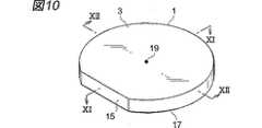
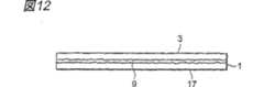
本発明に係る半導体基板の実施例1について、図10〜図13を参照して説明する。図10は実施例1に係る半導体基板1の斜視図であり、図11は図10に示す半導体基板1のXI−XI線に沿った断面図であり、図12は図10に示す半導体基板1のXII−XII線に沿った断面図であり、図13は図10に示す半導体基板1の表面に設けられたレーザマークの写真を表した図である。
実施例1に係る半導体基板1は、厚さ350μm、外径4インチの円板状のシリコンウェハであり、図10に示すように、半導体基板1の周縁部の一部が直線となるよう切り欠かれてオリエンテーションフラット(以下「OF」という)15が形成されている。
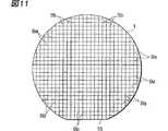
図11に示すように、半導体基板1の内部には、OF15に平行な方向に延びる切断起点領域9aが、半導体基板1の内部における外径の中心(以下「基準原点」という)から所定の間隔毎に複数形成されている。また、半導体基板1の内部には、OF15に垂直な方向に延びる切断起点領域9bが基準原点から所定の間隔毎に複数形成されている。切断起点領域9aは、図12に示すように、半導体基板1の内部にのみ形成され、半導体基板1の表面3及び裏面17には達していない。このことは、切断起点領域9bについても同様である。切断起点領域9a及び切断起点領域9bのそれぞれは、半導体基板1の内部に1列となるよう形成された溶融処理領域でもって形成されている。
図10に示すように、半導体基板1の表面3における基準原点直上の位置には、レーザマーク19が設けられている。このレーザマーク19とOF15との両者により、半導体基板1の内部に形成された切断起点領域9a及び切断起点領域9bの位置を把握することができる。すなわち、レーザマーク19とOF15との両者は、半導体基板1の内部に形成された切断起点領域9a及び切断起点領域9bの位置を識別するための識別マークとして機能する。なお、レーザマーク19の形成場所は、切断起点領域上に設ける他に、半導体基板に形成される回路等の機能部位以外の場所や、半導体基板の周縁部の半導体デバイスとして利用しない部位に形成してもよい。そして、レーザマーク19は、ソフトマーキングと呼ばれる発塵や熱影響のないクリーンなレーザマーキング方式によって半導体基板1の表面3を溶かし込むことで形成され、図13に示すように、レーザマーク19は直径1μmの凹状のものである。
次に、上述したレーザ加工装置100による半導体基板1の製造方法について、図9及び図14を参照して説明する。図14は半導体基板1の製造方法を説明するためのフローチャートである。
まず、半導体基板1の光吸収特性を図示しない分光光度計等により測定する。この測定結果に基づいて、半導体基板1の表面3にレーザマーク19を形成するためのレーザ光と、半導体基板1に対して透明な波長又は吸収の少ない波長のレーザ光Lとを発生するレーザ光源101をそれぞれ選定する(S101)。続いて、半導体基板1の厚さを測定する。厚さの測定結果及び半導体基板1の屈折率を基にして、半導体基板1のZ軸方向の移動量を決定する(S103)。これは、半導体基板1に対して透明な波長又は吸収の少ない波長のレーザ光Lの集光点Pを半導体基板1の内部に位置させるために、半導体基板1の表面3に位置するレーザ光Lの集光点Pを基準とした半導体基板1のZ軸方向の移動量である。この移動量は全体制御部127に入力される。
半導体基板1をレーザ加工装置100の載置台107の支持部材107a上に載置する。そして、観察用光源117から可視光を発生させて半導体基板1を照明する(S105)。照明された半導体基板1の表面3を撮像素子121により撮像する。撮像素子121により撮像された撮像データは撮像データ処理部125に送られる。この撮像データに基づいて撮像データ処理部125は観察用光源117の可視光の焦点が表面3に位置するような焦点データを演算する(S107)。
この焦点データはステージ制御部115に送られる。ステージ制御部115は、この焦点データを基にしてZ軸ステージ113をZ軸方向の移動させる(S109)。これにより、観察用光源117の可視光の焦点が半導体基板1の表面3に位置する。なお、撮像データ処理部125は、撮像データに基づいて半導体基板1の表面3の拡大画像データを演算する。この拡大画像データは全体制御部127を介してモニタ129に送られ、これによりモニタ129に半導体基板1の表面3の拡大画像が表示される。
続いて、半導体基板1のOF15の方向がYステージ111のストローク方向に一致するよう、θステージ108により半導体基板1を回転させる(S111)。さらに、半導体基板1の表面3にレーザマーク19を形成するためのレーザ光の集光点が、半導体基板1の表面3における基準原点直上の位置となるよう、X軸ステージ109、Y軸ステージ111及びZ軸ステージ113により半導体基板1を移動させる(S113)。この状態でレーザ光を照射し、半導体基板1の表面3における基準原点直上の位置にレーザマーク19を形成する(S115)。
その後、ステップS103で決定され全体制御部127に予め入力された移動量データが、ステージ制御部115に送られる。ステージ制御部115はこの移動量データに基づいて、レーザ光Lの集光点Pが半導体基板1の内部となる位置に、Z軸ステージ113により半導体基板1をZ軸方向に移動させる(S117)。
続いて、レーザ光源101からレーザ光Lを発生させて、レーザ光Lを半導体基板1に照射する。レーザ光Lの集光点Pは半導体基板1の内部に位置しているので、溶融処理領域は半導体基板1の内部にのみ形成される。そして、X軸ステージ109やY軸ステージ111により半導体基板1を移動させて、半導体基板1の内部に、OF15に平行な方向に延びる切断起点領域9a及びOF15に垂直な方向に延びる切断起点領域9bのそれぞれを、基準原点から所定の間隔毎に複数形成し(S119)、実施例1に係る半導体基板1が製造される。
なお、半導体基板1を赤外透過照明116による赤外線で照明すると共に、撮像データ処理部125により結像レンズ123及び撮像素子121の観察面を半導体基板1の内部に合わせれば、半導体基板1の内部に形成された切断起点領域9a及び切断起点領域9bを撮像して撮像データを取得し、モニタ129に表示させることもできる。
以上説明したように、実施例1に係る半導体基板1は、半導体基板1の内部に集光点Pが合わされ、集光点Pにおけるピークパワー密度が1×10⁸(W/cm2)以上で且つパルス幅が1μs以下の条件でレーザ光Lが照射されることで、半導体基板1の内部に多光子吸収による溶融処理領域が形成されている。この多光子吸収を発生し得るレーザ光Lの照射においては、半導体基板1の表面3ではレーザ光Lがほとんど吸収されないため、半導体基板1の表面3が溶融することはない。したがって、半導体デバイスの製造工程においては、従来通りの工程によって、半導体基板1の表面3に機能素子を形成することができる。なお、半導体基板1の裏面17も溶融されることはないので、半導体基板1の裏面17を半導体基板1の表面3と同様に扱うことができるのは勿論である。
また、実施例1に係る半導体基板1は、溶融処理領域でもって切断起点領域9a及び切断起点領域9bが半導体基板1の内部に形成されている。半導体基板1の内部に溶融処理領域が形成されていると、溶融処理領域を起点として比較的小さな力で半導体基板1に割れが発生するため、切断起点領域9a及び切断起点領域9bに沿って高い精度で半導体基板1を割って切断することができる。よって、半導体デバイスの製造工程においては、従来のような機能素子形成後の切削加工や加熱溶融加工が不要となり、例えば、切断起点領域9a及び切断起点領域9bに沿うよう半導体基板1の裏面17にナイフエッジを当てるだけで半導体基板1を切断することができる。したがって、機能素子形成後の半導体基板1の切断による機能素子の破壊を防止することができる。
さらに、実施例1に係る半導体基板1においては、レーザマーク19とOF15との両者が、半導体基板1の内部に形成された切断起点領域9a及び切断起点領域9bの位置の基準となっている。したがって、半導体デバイスの製造工程においては、レーザマーク19とOF15とに基づいて、半導体基板1の内部に形成された切断起点領域9a及び切断起点領域9bの位置を把握し、機能素子のパターンニングや半導体基板1の切断等を行うことができる。
なお、半導体基板1の内部に溶融処理領域が形成されると、意識的に外力を印加しなくても、溶融処理領域を起点として(すなわち、切断起点領域9a及び切断起点領域9bに沿って)、半導体基板1の内部に割れが発生する場合がある。この割れが半導体基板1の表面3及び裏面17に到達するか否かは、半導体基板1の厚さ方向における溶融処理領域の位置や、半導体基板1の厚さに対する溶融処理領域の大きさ等に関係する。したがって、半導体基板1の内部に形成する溶融処理領域の位置や大きさ等を調節することによって、半導体デバイスの製造工程において半導体基板1がハンドリングされたりヒートサイクルを経たりすることで、半導体基板1の表面3及び裏面17に割れが到達しないよう、或いは切断直前に半導体基板1の表面3及び裏面17に割れが到達するよう、種々の制御を行うことができる。
[半導体基板の実施例2]
本発明に係る半導体基板の実施例2について、図15〜図18を参照して説明する。実施例2に係る半導体基板1は、厚さ350μm、外径4インチの円板状のGaAsウェハであり、図15に示すように、半導体基板1の周縁部の一部が直線となるよう切り欠かれてOF15が形成されている。
この半導体基板1は、外縁に沿った外縁部31(図15の2点鎖線の外側部分)を有し、この外縁部31の内側部分32(図15の2点鎖線の内側部分)の内部には、実施例1に係る半導体基板1と同様に、OF15と平行な方向に延びる複数本の切断起点領域9aと、OF15に垂直な方向に延びる複数本の切断起点領域9bとが形成されている。このように、内側部分32の内部に切断起点領域9a,9bが格子状に形成されることで、内側部分32は多数の矩形状の区画部33に仕切られる。
半導体デバイスの製造工程においては、この区画部33毎に機能素子が形成され、その後、切断起点領域9a,9bに沿って半導体基板1が切断されて、各区画部33が個々の半導体チップに対応することとなる。
そして、図16に示すように、多数の区画部33のうち、外縁部31側に位置する区画部33の外縁部31側の角部分33aにおいては、切断起点領域9aと切断起点領域9bが交差して形成されている。すなわち、角部分33aにおいて、切断起点領域9aは切断起点領域9bを超えて終端しており、切断起点領域9bは切断起点領域9aを超えて終端している。なお、「多数の区画部33のうち、外縁部31側に位置する区画部33」とは、換言すれば「多数の区画部33のうち、外縁部31に隣接して形成された区画部33」ということもできる。
次に、実施例2に係る半導体基板1の製造方法について説明する。図17に示すように、半導体基板1の内側部分32と同等の形状を有する開口部35が形成されたマスク36を用意する。そして、内側部分32が開口部35から露出するように半導体基板1にマスク36を重ねる。これにより、半導体基板1の外縁部31がマスク36で覆われることになる。
この状態で、例えば上述のレーザ加工装置100を用いて、半導体基板1の内部に集光点を合わせてレーザ光を照射し、半導体基板1の内部に多光子吸収による溶融処理領域を形成することで、半導体基板1のレーザ光入射面(すなわち、マスク36の開口部35から露出する半導体基板1の表面)から所定距離内側に切断起点領域9a,9bを形成する。
このとき、レーザ光の走査ラインとなる切断予定ライン5を、OF15を基準として格子状に設定するが、各切断予定ライン5の始点5a及び終点5bをマスク36上に位置させれば、半導体基板1の内側部分32に対して確実に且つ同等の条件でレーザ光が照射されることになる。これにより、内側部分32の内部に形成される溶融処理領域をいずれの場所でもほぼ同等の形成状態とすることができ、精密な切断起点領域9a,9bを形成することが可能になる。
なお、マスク36を用いずに、半導体基板1の内側部分32と外縁部31との境界付近に各切断予定ライン5の始点5a及び終点5bを位置させて、各切断予定ライン5に沿ってレーザ光の照射を行うことにより、内側部分32の内部に切断起点領域9a,9bを形成することも可能である。
以上説明したように、実施例2に係る半導体基板1によれば、実施例1に係る半導体基板1と同様の理由により、半導体デバイスの製造工程において、半導体基板1の表面に機能素子を形成することができ、且つ機能素子形成後における半導体基板1の切断による機能素子の破壊を防止することができる。
しかも、半導体基板1の内側部分32の内部に切断起点領域9a,9bが形成され、外縁部31には切断起点領域9a,9bが形成されていないことから、半導体基板1全体としての機械的強度が向上することになる。したがって、半導体基板1の搬送工程や機能素子形成のための加熱工程等において、半導体基板1が不測の下に切断されてしまうという事態を防止することができる。
また、外縁部31側に位置する区画部33の角部分33aにおいては、切断起点領域9a,9bが交差して形成されているため、角部分33aにおいても、当該区画部33の他の部分と同様に切断起点領域9a,9bの形成が確実且つ良好なものとなる。したがって、半導体基板1を切断した際に当該区画部33に対応する半導体チップにチッピングやクラッキングが発生するのを防止することができる。
また、図18に示すように、切断起点領域9a,9bは半導体基板1の内部に収まり、外部には露出しないため、切断起点領域9a,9bを構成する溶融処理領域を形成する際にガスが発生するようなことも防止される。
さらに、切断起点領域9a,9bを構成する溶融処理領域が半導体基板1の内部に形成されていることで、不純物を捕獲するゲッタリング効果が期待され、半導体デバイスの製造工程において、重金属等の不純物をデバイス活性領域から取り除くことが可能になる。このことは、実施例1に係る半導体基板1についても同様である。
[半導体チップ、及び半導体デバイスの製造方法の実施例]
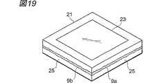
本発明に係る半導体チップ、及び半導体デバイスの製造方法の実施例について、図19を参照して説明する。図19は、実施例に係る半導体チップ21の斜視図である。
実施例1に係る半導体チップ21は、次に示すようにして形成されたものである。すなわち、上述した実施例1又は実施例2に係る半導体基板1を用い、半導体デバイスの製造工程において、半導体基板1の内部に形成された切断起点領域9a及び切断起点領域9bの位置をレーザマーク19とOF15とに基づいて把握し、パターンニングにより半導体基板1の表面3に複数の機能素子23を形成する。そして、プローブテスト等の検査工程を経た後に、レーザマーク19とOF15とに基づいて切断起点領域9a及び切断起点領域9bに沿うよう半導体基板1の裏面17にナイフエッジを当てて半導体基板1を切断し、半導体チップ21を得る。
このように形成された半導体チップ21は、図15に示すように、その周縁部が切断面25により囲まれており、半導体チップ21の端面のうち切断面25に切断起点領域9a又は切断起点領域9bを有している。切断起点領域9a及び切断起点領域9bは共に、溶融処理領域でもって形成されているため、半導体チップ21は、切断面25に溶融処理領域を有していることになる。
以上説明したように、実施例に係る半導体チップ21によれば、溶融処理領域により切断面25が保護されるため、切断面25におけるチッピングやクラッキングの発生を防止することができる。また、半導体チップ21の周縁部が切断面25により囲まれているため、半導体チップ21の周縁部が溶融処理領域により囲まれることとなり、これにより、半導体チップ21の抗折強度を向上させることができる。
以上、本発明の実施形態について詳細に説明したが、本発明は上記実施形態に限定されないことはいうまでもない。
上記実施形態では、半導体基板の内部に形成された切断起点領域の位置を識別するための識別マークとして、半導体基板の表面にレーザマーク及びOFを設けたが、例えば、レーザマークを複数設けたり、或いはラインを引いたり等、種々の方法で半導体基板の表面に識別マークを設けることができる。
また、上記実施形態は、切断起点領域が半導体基板の内部に格子状に形成された場合であったが、切断起点領域はレーザ加工により形成されるため、任意の形状のラインに沿って切断起点領域を形成することができる。
さらに、上記実施形態の半導体チップは、周縁部が切断面で囲まれたものであったが、周縁部の一部のみが切断面であっても、溶融処理領域により切断面におけるチッピングやクラッキングの発生が防止され、半導体チップの抗折強度が向上することとなる。
産業上の利用可能性
以上説明したように、本発明によれば、レーザ光の照射により当該レーザ光の集光点の位置で形成される多光子吸収による改質領域が、半導体基板の内部に形成されている。すなわち、この改質領域は、レーザ光の集光点が半導体基板の内部に合わされ、当該集光点の位置で多光子吸収という現象が発生することで、半導体基板の内部に形成される。この多光子吸収を発生し得るレーザ光の照射においては、半導体基板の表面ではレーザ光がほとんど吸収されないため、半導体基板の表面が溶融することはない。したがって、半導体デバイスの製造工程において、従来通り半導体基板の表面に機能素子を形成することができる。
さらに、本発明によれば、改質領域によって切断起点領域が半導体基板の内部に形成されている。半導体基板の内部に改質領域が形成されていると、改質領域を起点として比較的小さな力で半導体基板に割れが発生するため、切断起点領域に沿って高い精度で半導体基板を割って切断することができる。したがって、半導体デバイスの製造工程において、従来のような機能素子形成後の切削加工や加熱溶融加工が不要となり、半導体基板の切断による機能素子の破壊を防止することができる。
【図面の簡単な説明】
図1は、本実施形態に係るレーザ加工方法によるレーザ加工中の半導体基板の平面図である。
図2は、図1に示す半導体基板のII−II線に沿った断面図である。
図3は、本実施形態に係るレーザ加工方法によるレーザ加工後の半導体基板の平面図である。
図4は、図3に示す半導体基板のIV−IV線に沿った断面図である。
図5は、図3に示す半導体基板のV−V線に沿った断面図である。
図6は、本実施形態に係るレーザ加工方法により切断された半導体基板の平面図である。
図7は、本実施形態に係るレーザ加工方法により切断されたシリコンウェハの一部における断面の写真を表した図である。
図8は、本実施形態に係るレーザ加工方法におけるレーザ光の波長とシリコン基板の内部の透過率との関係を示すグラフである。
図9は、本実施形態に係るレーザ加工装置の概略構成図である。
図10は、実施例1に係る半導体基板の斜視図である。
図11は、図10に示す半導体基板のXI−XI線に沿った断面図である。
図12は、図10に示す半導体基板のXII−XII線に沿った断面図である。
図13は、図10に示す半導体基板の表面に設けられたレーザマークの写真を表した図である。
図14は、実施例1に係る半導体基板の製造方法を説明するためのフローチャートである。
図15は、実施例2に係る半導体基板の平面図である。
図16は、図15に示す半導体基板の要部拡大図である。
図17は、図15に示す半導体基板の製造方法を説明するための平面図である。
図18は、図15に示す半導体基板のXVIII−XVIII線に沿った断面図である。
図19は、実施例に係る半導体チップの斜視図である。Technical field
The present invention relates to a semiconductor substrate, a semiconductor chip, and a method for manufacturing a semiconductor device that are suitably used for manufacturing a semiconductor device.
Background art
In a semiconductor device manufacturing process, it is common to form a plurality of functional elements on a semiconductor substrate such as a silicon wafer and then cut the semiconductor substrate into functional elements with a diamond blade (cutting) to obtain a semiconductor chip. It is.
Further, instead of cutting with the diamond blade, the semiconductor substrate may be cut by heating and melting by irradiating the semiconductor substrate with laser light having absorbency with respect to the semiconductor substrate (heating and melting process).
Disclosure of the invention
However, since the cutting of the semiconductor substrate by the above-described cutting process or heat-melting process is performed after the functional element is formed on the semiconductor substrate, the functional element may be destroyed due to heat generated during the cutting, for example.
Therefore, the present invention has been made in view of such circumstances, and there is provided a semiconductor substrate, a semiconductor chip, and a semiconductor device that can prevent a functional element from being destroyed by cutting in a semiconductor device manufacturing process. An object is to provide a manufacturing method.
In order to achieve the above object, the semiconductor substrate according to the present invention has a cutting origin region formed therein by a modified region formed by multiphoton absorption that is formed at the position of the focal point of the laser beam by irradiation with the laser beam. It is characterized by being.
According to this semiconductor substrate, the modified region by multiphoton absorption formed at the position of the condensing point of the laser beam by irradiation of the laser beam is formed inside the semiconductor substrate. In other words, the modified region is formed inside the semiconductor substrate by causing the focal point of the laser beam to be aligned inside the semiconductor substrate and causing the phenomenon of multiphoton absorption at the position of the focal point. In the irradiation of laser light that can generate multiphoton absorption, the laser light is hardly absorbed on the surface of the semiconductor substrate, so that the surface of the semiconductor substrate does not melt. Therefore, in the semiconductor device manufacturing process, the functional element can be formed on the surface of the semiconductor substrate as usual. Furthermore, according to this semiconductor substrate, the cutting start region is formed inside the semiconductor substrate by the modified region. If a modified region is formed inside the semiconductor substrate, the semiconductor substrate cracks with a relatively small force starting from the modified region, so the semiconductor substrate is divided and cut along the cutting origin region with high accuracy. can do. Therefore, in the manufacturing process of the semiconductor device, the cutting process and the heat-melting process after forming the functional element as in the prior art are not required, and the functional element can be prevented from being broken by cutting the semiconductor substrate.
Here, the condensing point is a portion where the laser beam is condensed. The functional element means a light receiving element such as a photodiode, a light emitting element such as a laser diode, or a circuit element formed as a circuit. Further, the cutting starting point region means a region that becomes a starting point of cutting when the semiconductor substrate is cut. Therefore, the cutting start region is a planned cutting portion where cutting is planned in the semiconductor substrate. The cutting start region may be formed by continuously forming the modified region, or may be formed by intermittently forming the modified region.
In addition, the semiconductor substrate according to the present invention has a peak power density at the focal point of 1 × 10.8(W / cm2) The cutting start region is formed inside by the modified region including the fusion processing region formed at the position of the condensing point of the laser beam by irradiation of the laser beam under the above condition and the pulse width of 1 μs or less. It is characterized by being.
According to this semiconductor substrate, the peak power density at the focal point is 1 × 10.8(W / cm2) A modified region including a melt-processed region formed at the position of the condensing point of the laser beam by irradiation with the laser beam under the above conditions and a pulse width of 1 μs or less is formed inside the semiconductor substrate. . That is, in this melting processing region, the focal point of the laser beam is set inside the semiconductor substrate, and the phenomenon of multiphoton absorption occurs at the position of the focal point and is locally heated. Formed. Since this melting treatment region is an example of the above-described modified region, this semiconductor substrate can also form a functional element on the surface of the semiconductor substrate in the semiconductor device manufacturing process, and the semiconductor after the functional element is formed. It is possible to prevent the functional element from being broken by cutting the substrate.
Further, the semiconductor substrate according to the present invention is characterized in that a cutting start region is formed inside by a modified region formed at the position of the condensing point of the laser beam by irradiation of the laser beam. The modified region may be a melt-processed region.
According to this semiconductor substrate, for the same reason as the semiconductor substrate according to the present invention described above, the functional element can be formed on the surface of the semiconductor substrate in the manufacturing process of the semiconductor device, and the semiconductor substrate after the functional element is formed. It is possible to prevent the functional element from being broken by cutting. However, the formation of the modified region may be caused by multiphoton absorption or may be caused by others.
In addition, the semiconductor substrate according to the present invention has an outer edge portion along the outer edge, and a cutting start region is formed inside the inner portion of the outer edge portion by a modified region.
According to this semiconductor substrate, for the same reason as the semiconductor substrate according to the present invention described above, the functional element can be formed on the surface of the semiconductor substrate in the manufacturing process of the semiconductor device, and the semiconductor substrate after the functional element is formed. It is possible to prevent the functional element from being broken by cutting. In addition, by forming a cutting starting region inside the inner portion of the outer edge portion of the semiconductor substrate, it is possible to prevent unintentional cutting of the semiconductor substrate in a semiconductor substrate transport process or a heating process for functional element formation. become.
At this time, the cutting start region is formed in a lattice shape, and among the partitioning portions partitioned by the cutting starting region, the cutting starting region is formed to intersect at the corner portion of the partitioning portion located on the outer edge side. It is preferable. Thereby, also in the corner part of the partition part located on the outer edge part side, the formation of the cutting start region is assured and good like the other parts of the partition part, and the partition part is cut when the semiconductor substrate is cut. It is possible to prevent chipping and cracking from occurring in the semiconductor chip corresponding to the above. Here, the term “lattice” means not only the case where the cutting start point regions extending in two orthogonal directions intersect, but also the case where the cutting start point regions extending in two different directions intersect. In addition, the term “intersection” is not limited to the case where the cutting start areas along two different directions intersect each other directly, but the case where the cutting start areas along two different directions intersect three-dimensionally (that is, in a twisted relationship). )).
Further, it is preferable that an identification mark for identifying the position of the cutting start region formed inside the semiconductor substrate is provided on the surface of the semiconductor substrate. Although the cutting start region is formed inside the semiconductor substrate, an identification mark for identifying the position of the cutting start region is provided on the surface of the semiconductor substrate. It is possible to grasp the position of the cutting start region formed on the substrate based on the recognition mark and perform patterning of the functional element, cutting of the semiconductor substrate, and the like.
In order to achieve the above object, a semiconductor chip according to the present invention forms a modified region by multiphoton absorption inside a semiconductor substrate by irradiating a laser beam with a focusing point inside the semiconductor substrate. The modified region is formed by cutting the semiconductor substrate using the modified region as a starting point region, and has a modified region on the cut surface by the cutting.
According to this semiconductor chip, since the cut surface is protected by the modified region, occurrence of chipping and cracking on the cut surface can be prevented. Further, when the peripheral edge of the semiconductor chip is surrounded by the cut surface, the peripheral edge of the semiconductor chip is surrounded by the modified region, thereby improving the bending strength of the semiconductor chip.
In addition, the semiconductor chip according to the present invention has a condensing point inside the semiconductor substrate, and the peak power density at the condensing point is 1 × 10.8(W / cm2) By irradiating laser light under the above conditions with a pulse width of 1 μs or less, a modified region including a melt-processed region is formed inside the semiconductor substrate, and the modified region including the melt-processed region is cut starting region The semiconductor substrate is formed by cutting a semiconductor substrate, and has a modified region including a melt-processed region on a cut surface by the cutting.
Since the melt processing region in this semiconductor chip is an example of the above-described modified region, this semiconductor chip can prevent chipping and cracking on the cut surface, and the peripheral portion of the semiconductor chip can be prevented by the cut surface. When surrounded, the bending strength of the semiconductor chip can be improved.
In addition, the semiconductor chip according to the present invention forms a modified region in the semiconductor substrate by irradiating a laser beam with a condensing point inside the semiconductor substrate, and uses the modified region as a cutting start region. It is formed by cutting a semiconductor substrate, and has a modified region on a cut surface by cutting. The modified region may be a melt-processed region.
According to this semiconductor chip, for the same reason as the semiconductor chip according to the present invention described above, it is possible to prevent the occurrence of chipping and cracking on the cut surface, and the peripheral portion of the semiconductor chip is surrounded by the cut surface. In this case, the bending strength of the semiconductor chip can be improved. However, the formation of the modified region may be caused by multiphoton absorption or may be caused by others.
In addition, the semiconductor chip according to the present invention is characterized in that a modified region including a melt processing region is formed on an end surface.
According to this semiconductor chip, it is possible to prevent the occurrence of chipping and cracking at the end face such as a cut surface due to the cutting of the semiconductor substrate, and to surround the periphery of the semiconductor chip with the modified region, the bending strength of the semiconductor chip Can be improved.
As described above, the method for manufacturing a semiconductor device according to the present invention irradiates a laser beam with a focusing point inside the semiconductor substrate, and forms a modified region by multiphoton absorption inside the semiconductor substrate. Depending on the region, a functional element is formed on the semiconductor substrate after the step of forming the cutting start region within a predetermined distance from the laser light incident surface of the semiconductor substrate along the planned cutting line of the semiconductor substrate and the step of forming the cutting start region The structure provided with a process and the process of cut | disconnecting a semiconductor substrate along a cutting | disconnection origin area | region after the process of forming a functional element can be taken. The modified region may be a melt-processed region.
Further, the semiconductor device manufacturing method according to the present invention is configured such that a laser beam is irradiated with a focusing point inside the semiconductor substrate, a modified region is formed inside the semiconductor substrate, and the semiconductor substrate is formed by the modified region. Forming a cutting start region within a predetermined distance from the laser light incident surface of the semiconductor substrate along a predetermined cutting line, forming a functional element on the semiconductor substrate after forming the cutting start region, and a functional device And a step of cutting the semiconductor substrate along the cutting start region after the step of forming. The modified region may be a melt-processed region.
BEST MODE FOR CARRYING OUT THE INVENTION
DESCRIPTION OF EMBODIMENTS Hereinafter, preferred embodiments of the present invention will be described in detail with reference to the drawings. When configuring the semiconductor substrate and the semiconductor chip according to the present embodiment, the semiconductor substrate is irradiated with laser light with the focusing point aligned inside, and a modified region by multiphoton absorption is formed inside the semiconductor substrate. Use laser processing methods. This laser processing method, particularly multiphoton absorption, will be described first.
Band gap E of material absorptionGIf the photon energy hv is smaller than that, it becomes optically transparent. Therefore, the condition for absorption in the material is hν> EGIt is. However, even if it is optically transparent, if the intensity of the laser beam is made very large, nhν> EGUnder these conditions (n = 2, 3, 4,...), Absorption occurs in the material. This phenomenon is called multiphoton absorption. In the case of a pulse wave, the intensity of the laser beam is the peak power density (W / cm at the condensing point of the laser beam).2), For example, the peak power density is 1 × 10⁸(W / cm2) Multiphoton absorption occurs under the above conditions. The peak power density is determined by (energy per pulse of laser light at the condensing point) / (laser beam cross-sectional area of laser light × pulse width). In the case of a continuous wave, the intensity of the laser beam is the electric field intensity (W / cm at the focal point of the laser beam).2)
The principle of laser processing according to this embodiment using such multiphoton absorption will be described with reference to FIGS. FIG. 1 is a plan view of the
The condensing point P is moved along the planned cutting line 5 by relatively moving the laser light L along the planned cutting line 5 (that is, along the direction of the arrow A). Thereby, as shown in FIGS. 3 to 5, the modified region 7 is formed only inside the
In the cutting of the
Note that the following two methods are conceivable for cutting the semiconductor substrate starting from the cutting start region. One is a case where after the cutting start region is formed, an artificial force is applied to the semiconductor substrate, so that the semiconductor substrate is cracked from the cutting start region and the semiconductor substrate is cut. This is cutting when the thickness of the semiconductor substrate is large, for example. An artificial force is applied when, for example, bending stress or shear stress is applied to the semiconductor substrate along the cutting start region of the semiconductor substrate, or thermal stress is generated by applying a temperature difference to the semiconductor substrate. That is. The other one is a case where by forming the cutting start region, the semiconductor substrate is naturally cracked from the cutting start region to the cross-sectional direction (thickness direction) of the semiconductor substrate, and as a result, the semiconductor substrate is cut. . For example, when the thickness of the semiconductor substrate is small, the cutting start region is formed by one row of modified regions, and when the thickness of the semiconductor substrate is large, a plurality of regions can be formed in the thickness direction. This is made possible by forming the cutting start region by the reformed regions formed in a row. In addition, even when this breaks naturally, in the part to be cut, the part corresponding to the part where the cutting starting point region is formed without cracking ahead on the surface of the part corresponding to the part where the cutting starting point region is not formed Since it is possible to cleave only, the cleaving can be controlled well. In recent years, since the thickness of a semiconductor substrate such as a silicon wafer tends to be thin, such a cleaving method with good controllability is very effective.
Now, as the modified region formed by multiphoton absorption in the present embodiment, there is a melting processing region described below.
The focusing point is set inside the semiconductor substrate, and the electric field intensity at the focusing point is 1 × 10.8(W / cm2) Irradiation with laser light is performed under the above conditions with a pulse width of 1 μs or less. As a result, the inside of the semiconductor substrate is locally heated by multiphoton absorption. By this heating, a melt processing region is formed inside the semiconductor substrate. The melt processing region is a region once solidified after melting, a region in a molten state, a region in which the material is re-solidified from a molten state, and can also be referred to as a phase-changed region or a region in which the crystal structure has changed. The melt treatment region can also be referred to as a region in which one structure is changed to another structure in a single crystal structure, an amorphous structure, or a polycrystalline structure. In other words, for example, a region changed from a single crystal structure to an amorphous structure, a region changed from a single crystal structure to a polycrystalline structure, or a region changed from a single crystal structure to a structure including an amorphous structure and a polycrystalline structure. To do. When the semiconductor substrate has a silicon single crystal structure, the melt processing region has, for example, an amorphous silicon structure. As an upper limit value of the electric field strength, for example, 1 × 10¹²(W / cm2). The pulse width is preferably 1 ns to 200 ns, for example.
The inventor has confirmed through experiments that a melt-processed region is formed inside a silicon wafer. The experimental conditions are as follows.
(A) Semiconductor substrate: silicon wafer (thickness 350 μm,
(B) Laser
Light source: Semiconductor laser pumped Nd: YAG laser
Wavelength: 1064nm
Laser beam spot cross-sectional area: 3.14 × 10⁻⁸cm2
Oscillation form: Q switch pulse
Repeat frequency: 100 kHz
Pulse width: 30ns
Output: 20μJ / pulse
Laser light quality: TEM00
Polarization characteristics: linearly polarized light
(C) Condensing lens
Magnification: 50 times
N. A. : 0.55
Transmittance to laser light wavelength: 60 percent
(D) Moving speed of the mounting table on which the semiconductor substrate is mounted: 100 mm / second
FIG. 7 is a view showing a photograph of a cross section of a part of a silicon wafer cut by laser processing under the above conditions. A
The fact that the
For example, when the thickness of the silicon substrate is 500 μm or less at the wavelength of the Nd: YAG laser of 1064 nm, it can be seen that the laser light is transmitted by 80% or more inside the silicon substrate. Since the thickness of the silicon wafer 11 shown in FIG. 7 is 350 μm, the
Silicon wafers are cracked in the cross-sectional direction starting from the cutting start region formed by the melt processing region, and the cracks reach the front and back surfaces of the silicon wafer, resulting in cutting. Is done. The cracks that reach the front and back surfaces of the silicon wafer may grow naturally or may grow by applying force to the silicon wafer. In addition, when a crack naturally grows from the cutting start region to the front and back surfaces of the silicon wafer, the case where the crack grows from a state where the melt treatment region forming the cutting starting region is melted, and the cutting starting region There are both cases where cracks grow when the solidified region is melted from the molten state. However, in both cases, the melt processing region is formed only inside the silicon wafer, and the melt processing region is formed only inside the cut surface after cutting as shown in FIG. When the cutting start region is formed in the semiconductor substrate by the melt processing region, unnecessary cracks that are off the cutting start region line are unlikely to occur during cleaving, so that cleaving control is facilitated.
As described above, the case of the melt processing region has been described as the modified region formed by multiphoton absorption. However, if the cutting origin region is formed as follows in consideration of the crystal structure of the semiconductor substrate and its cleavage property, the It becomes possible to cut the semiconductor substrate with a smaller force and with high accuracy starting from the cutting start region.
That is, in the case of a substrate made of a single crystal semiconductor having a diamond structure such as silicon, the cutting start region is formed in a direction along the (111) plane (first cleavage plane) or the (110) plane (second cleavage plane). Is preferred. In the case of a substrate made of a zinc-blende-type III-V group compound semiconductor such as GaAs, it is preferable to form the cutting start region in the direction along the (110) plane.
Note that the semiconductor substrate is oriented along a direction in which the above-described cutting start region is to be formed (for example, a direction along the (111) plane in the single crystal silicon substrate) or a direction perpendicular to the direction in which the cutting start region is to be formed. If a flat is formed, it becomes possible to easily and accurately form the cutting start region along the direction in which the cutting start region is to be formed on the semiconductor substrate by using the orientation flat as a reference.
A laser processing apparatus used in the laser processing method described above will be described with reference to FIG. FIG. 9 is a schematic configuration diagram of the
The
The mounting table 107 transmits infrared light through the
Since the Z-axis direction is a direction orthogonal to the
The
The
The
The
Data from the
Hereinafter, the present invention will be described more specifically with reference to examples.
[Example 1 of Semiconductor Substrate]
Example 1 of the semiconductor substrate according to the present invention will be described with reference to FIGS. 10 is a perspective view of the
The
As shown in FIG. 11, a cutting
As shown in FIG. 10, a
Next, a method for manufacturing the
First, the light absorption characteristics of the
The
This focus data is sent to the
Subsequently, the
Thereafter, the movement amount data determined in step S103 and input in advance to the
Subsequently, laser light L is generated from the
If the
As described above, in the
Further, in the
Further, in the
Note that, when the melt processing region is formed inside the
[Example 2 of semiconductor substrate]
Example 2 of the semiconductor substrate according to the present invention will be described with reference to FIGS. The
This
In the manufacturing process of the semiconductor device, a functional element is formed for each
And in the corner |
Next, a method for manufacturing the
In this state, for example, by using the
At this time, the planned cutting lines 5 serving as the laser light scanning lines are set in a lattice pattern with the
In addition, without using the
As described above, according to the
In addition, since the cutting
Further, in the
Further, as shown in FIG. 18, since the cutting
Further, since the melt processing regions constituting the cutting
[Embodiments of Semiconductor Chip and Semiconductor Device Manufacturing Method]
An embodiment of a semiconductor chip and a method for manufacturing a semiconductor device according to the present invention will be described with reference to FIG. FIG. 19 is a perspective view of the
The
As shown in FIG. 15, the peripheral portion of the
As described above, according to the
As mentioned above, although embodiment of this invention was described in detail, it cannot be overemphasized that this invention is not limited to the said embodiment.
In the above embodiment, the laser mark and OF are provided on the surface of the semiconductor substrate as an identification mark for identifying the position of the cutting start region formed inside the semiconductor substrate.For example, a plurality of laser marks may be provided, Alternatively, an identification mark can be provided on the surface of the semiconductor substrate by various methods such as drawing a line.
Moreover, although the said embodiment was a case where a cutting | disconnection origin area | region was formed in the inside of a semiconductor substrate at the grid | lattice form, since a cutting | disconnection origin area | region is formed by laser processing, it is a cutting | disconnection origin on the line of arbitrary shapes. Regions can be formed.
Furthermore, although the semiconductor chip of the above embodiment has a peripheral portion surrounded by a cut surface, even if only a part of the peripheral portion is a cut surface, chipping and cracking on the cut surface is caused by the melt processing region. Generation | occurrence | production is prevented and the bending strength of a semiconductor chip will improve.
Industrial applicability
As described above, according to the present invention, the modified region by multiphoton absorption formed at the position of the condensing point of the laser beam by the irradiation of the laser beam is formed inside the semiconductor substrate. In other words, the modified region is formed inside the semiconductor substrate by causing the focal point of the laser beam to be aligned inside the semiconductor substrate and causing the phenomenon of multiphoton absorption at the position of the focal point. In the irradiation of laser light that can generate multiphoton absorption, the laser light is hardly absorbed on the surface of the semiconductor substrate, so that the surface of the semiconductor substrate does not melt. Therefore, in the semiconductor device manufacturing process, the functional element can be formed on the surface of the semiconductor substrate as usual.
Furthermore, according to the present invention, the cutting start region is formed inside the semiconductor substrate by the modified region. If a modified region is formed inside the semiconductor substrate, the semiconductor substrate cracks with a relatively small force starting from the modified region, so the semiconductor substrate is divided and cut along the cutting origin region with high accuracy. can do. Therefore, in the manufacturing process of the semiconductor device, the cutting process and the heat-melting process after forming the functional element as in the prior art are not required, and the functional element can be prevented from being broken by cutting the semiconductor substrate.
[Brief description of the drawings]
FIG. 1 is a plan view of a semiconductor substrate during laser processing by the laser processing method according to the present embodiment.
2 is a cross-sectional view taken along line II-II of the semiconductor substrate shown in FIG.
FIG. 3 is a plan view of the semiconductor substrate after laser processing by the laser processing method according to the present embodiment.
4 is a cross-sectional view taken along line IV-IV of the semiconductor substrate shown in FIG.
FIG. 5 is a sectional view taken along line VV of the semiconductor substrate shown in FIG.
FIG. 6 is a plan view of a semiconductor substrate cut by the laser processing method according to the present embodiment.
FIG. 7 is a view showing a photograph of a cross section of a part of a silicon wafer cut by the laser processing method according to the present embodiment.
FIG. 8 is a graph showing the relationship between the wavelength of laser light and the transmittance inside the silicon substrate in the laser processing method according to the present embodiment.
FIG. 9 is a schematic configuration diagram of a laser processing apparatus according to the present embodiment.
FIG. 10 is a perspective view of the semiconductor substrate according to the first embodiment.
FIG. 11 is a cross-sectional view taken along line XI-XI of the semiconductor substrate shown in FIG.
12 is a sectional view taken along line XII-XII of the semiconductor substrate shown in FIG.
FIG. 13 is a view showing a photograph of a laser mark provided on the surface of the semiconductor substrate shown in FIG.
FIG. 14 is a flowchart for explaining the method of manufacturing the semiconductor substrate according to the first embodiment.
FIG. 15 is a plan view of the semiconductor substrate according to the second embodiment.
FIG. 16 is an enlarged view of a main part of the semiconductor substrate shown in FIG.
FIG. 17 is a plan view for explaining the method for manufacturing the semiconductor substrate shown in FIG.
18 is a cross-sectional view taken along line XVIII-XVIII of the semiconductor substrate shown in FIG.
FIG. 19 is a perspective view of the semiconductor chip according to the example.
Claims (16)
Translated fromJapanese前記切断起点領域により仕切られた区画部のうち、前記外縁部側に位置する前記区画部の角部分においては、前記切断起点領域が交差して形成されていることを特徴とする請求項5記載の半導体基板。The cutting origin region is formed in a lattice shape,
6. The cutting starting point region is formed so as to intersect at a corner portion of the dividing portion located on the outer edge side among the partitioning portions partitioned by the cutting starting point region. Semiconductor substrate.
前記切断による切断面に前記改質領域を有している、
ことを特徴とする半導体チップ。By irradiating a laser beam with a focusing point inside the semiconductor substrate, a modified region by multiphoton absorption is formedonly inside the semiconductor substrate, and the modified region is used as a cutting origin region of the semiconductor substrate. Formed by cutting,
Having the modified region on the cut surface by the cutting,
A semiconductor chip characterized by that.
前記切断による切断面に、前記溶融処理領域を含む改質領域を有している、
ことを特徴とする半導体チップ。By aligning the condensing point inside the semiconductor substrate and irradiating the laser beam under conditions where the peak power density at the condensing point is 1 × 10⁸ (W / cm2 ) or more and the pulse width is 1 μs or less, Formed by forming a modified region including a melt treatment regiononly inside the semiconductor substrate, and cutting the semiconductor substrate using the modified region including the melt treatment region as a cutting origin region,
In the cut surface by the cutting, it has a modified region including the melting treatment region,
A semiconductor chip characterized by that.
前記切断による切断面に前記改質領域を有している、
ことを特徴とする半導体チップ。Forming a modified regiononly inside the semiconductor substrate by aligning a condensing point inside the semiconductor substrate and irradiating the laser beam, and cutting the semiconductor substrate using the modified region as a cutting origin region Formed with
Having the modified region on the cut surface by the cutting,
A semiconductor chip characterized by that.
前記切断起点領域を形成する工程後、前記半導体基板に機能素子を形成する工程と、
前記機能素子を形成する工程後、前記切断起点領域に沿って前記半導体基板を切断する工程と、
を備えることを特徴とする半導体デバイスの製造方法。A semiconductor substrate is irradiated with a laser beam with a converging point aligned, and a modified region by multiphoton absorption is formed inside the semiconductor substrate, and along the planned cutting line of the semiconductor substrate by the modified region Forming a cutting origin region on a predetermined distance from the laser light incident surface of the semiconductor substrate;
After the step of forming the cutting start region, forming a functional element on the semiconductor substrate;
After the step of forming the functional element, the step of cutting the semiconductor substrate along the cutting start region,
A method for manufacturing a semiconductor device, comprising:
前記切断起点領域を形成する工程後、前記半導体基板に機能素子を形成する工程と、
前記機能素子を形成する工程後、前記切断起点領域に沿って前記半導体基板を切断する工程と、
を備えることを特徴とする半導体デバイスの製造方法。The semiconductor substrate is irradiated with a laser beam with a focusing point aligned, and a modified region is formed inside the semiconductor substrate. By the modified region, along the planned cutting line of the semiconductor substrate, the semiconductor substrate A step of forming a cutting start region inside a predetermined distance from the laser light incident surface;
After the step of forming the cutting start region, forming a functional element on the semiconductor substrate;
After the step of forming the functional element, the step of cutting the semiconductor substrate along the cutting start region,
A method for manufacturing a semiconductor device, comprising:
前記機能素子を形成する工程後、前記切断起点領域に沿って前記半導体基板を切断する工程と、
を備えることを特徴とする半導体デバイスの製造方法。Forming a functional element on a semiconductor substrate in which a cutting origin region is formed inside by a modified region formed at a position of a condensing point of the laser beam by irradiation of the laser beam;
After the step of forming the functional element, the step of cutting the semiconductor substrate along the cutting start region,
A method for manufacturing a semiconductor device, comprising:
Applications Claiming Priority (3)
| Application Number | Priority Date | Filing Date | Title |
|---|---|---|---|
| JP2002067348 | 2002-03-12 | ||
| JP2002067348 | 2002-03-12 | ||
| PCT/JP2003/002866WO2003076118A1 (en) | 2002-03-12 | 2003-03-11 | Semiconductor substrate, semiconductor chip, and semiconductor device manufacturing method |
Related Child Applications (3)
| Application Number | Title | Priority Date | Filing Date |
|---|---|---|---|
| JP2005045950ADivisionJP3761566B2 (en) | 2002-03-12 | 2005-02-22 | Manufacturing method of semiconductor chip |
| JP2006069936ADivisionJP3990711B2 (en) | 2002-03-12 | 2006-03-14 | Laser processing equipment |
| JP2006069929ADivisionJP3990710B2 (en) | 2002-03-12 | 2006-03-14 | Laser processing method |
Publications (2)
| Publication Number | Publication Date |
|---|---|
| JPWO2003076118A1 JPWO2003076118A1 (en) | 2005-06-30 |
| JP4509573B2true JP4509573B2 (en) | 2010-07-21 |
Family
ID=27800280
Family Applications (1)
| Application Number | Title | Priority Date | Filing Date |
|---|---|---|---|
| JP2003574373AExpired - LifetimeJP4509573B2 (en) | 2002-03-12 | 2003-03-11 | Semiconductor substrate, semiconductor chip, and semiconductor device manufacturing method |
Country Status (4)
| Country | Link |
|---|---|
| JP (1) | JP4509573B2 (en) |
| AU (1) | AU2003211575A1 (en) |
| TW (1) | TWI289890B (en) |
| WO (1) | WO2003076118A1 (en) |
Cited By (4)
| Publication number | Priority date | Publication date | Assignee | Title |
|---|---|---|---|---|
| US10562130B1 (en) | 2018-12-29 | 2020-02-18 | Cree, Inc. | Laser-assisted method for parting crystalline material |
| US10576585B1 (en) | 2018-12-29 | 2020-03-03 | Cree, Inc. | Laser-assisted method for parting crystalline material |
| US10611052B1 (en) | 2019-05-17 | 2020-04-07 | Cree, Inc. | Silicon carbide wafers with relaxed positive bow and related methods |
| US11024501B2 (en) | 2018-12-29 | 2021-06-01 | Cree, Inc. | Carrier-assisted method for parting crystalline material along laser damage region |
Families Citing this family (25)
| Publication number | Priority date | Publication date | Assignee | Title |
|---|---|---|---|---|
| JP4659300B2 (en) | 2000-09-13 | 2011-03-30 | 浜松ホトニクス株式会社 | Laser processing method and semiconductor chip manufacturing method |
| WO2003076119A1 (en) | 2002-03-12 | 2003-09-18 | Hamamatsu Photonics K.K. | Method of cutting processed object |
| EP2400539B1 (en) | 2002-03-12 | 2017-07-26 | Hamamatsu Photonics K.K. | Substrate dividing method |
| TWI326626B (en) | 2002-03-12 | 2010-07-01 | Hamamatsu Photonics Kk | Laser processing method |
| TWI520269B (en) | 2002-12-03 | 2016-02-01 | Hamamatsu Photonics Kk | Cutting method of semiconductor substrate |
| FR2852250B1 (en) | 2003-03-11 | 2009-07-24 | Jean Luc Jouvin | PROTECTIVE SHEATH FOR CANNULA, AN INJECTION KIT COMPRISING SUCH ANKLE AND NEEDLE EQUIPPED WITH SUCH ANKLE |
| DE60315515T2 (en) | 2003-03-12 | 2007-12-13 | Hamamatsu Photonics K.K., Hamamatsu | LASER PROCESSING PROCEDURES |
| JP4563097B2 (en) | 2003-09-10 | 2010-10-13 | 浜松ホトニクス株式会社 | Semiconductor substrate cutting method |
| JP2005109324A (en)* | 2003-10-01 | 2005-04-21 | Tokyo Seimitsu Co Ltd | Laser beam dicing device |
| JP4917257B2 (en) | 2004-11-12 | 2012-04-18 | 浜松ホトニクス株式会社 | Laser processing method |
| JP4198123B2 (en)* | 2005-03-22 | 2008-12-17 | 浜松ホトニクス株式会社 | Laser processing method |
| JP2007227768A (en)* | 2006-02-24 | 2007-09-06 | Denso Corp | Method of dicing semiconductor wafer |
| JP2007235069A (en)* | 2006-03-03 | 2007-09-13 | Tokyo Seimitsu Co Ltd | Wafer machining method |
| JP2007235068A (en)* | 2006-03-03 | 2007-09-13 | Tokyo Seimitsu Co Ltd | Wafer machining method |
| JP4804183B2 (en)* | 2006-03-20 | 2011-11-02 | 株式会社デンソー | Semiconductor substrate dividing method and semiconductor chip manufactured by the dividing method |
| JP2007287976A (en)* | 2006-04-18 | 2007-11-01 | Denso Corp | Semiconductor substrate |
| JP5098229B2 (en)* | 2006-06-21 | 2012-12-12 | ソニー株式会社 | Surface modification method |
| JP5164363B2 (en)* | 2006-10-27 | 2013-03-21 | 株式会社ディスコ | Manufacturing method of semiconductor wafer |
| JP5134928B2 (en) | 2007-11-30 | 2013-01-30 | 浜松ホトニクス株式会社 | Workpiece grinding method |
| JP5054496B2 (en) | 2007-11-30 | 2012-10-24 | 浜松ホトニクス株式会社 | Processing object cutting method |
| TW201207913A (en)* | 2010-08-13 | 2012-02-16 | Msscorps Co Ltd | Two-stage encapsulation removing method for semiconductor device and laser grooving device |
| JP2014236034A (en)* | 2013-05-31 | 2014-12-15 | 株式会社ディスコ | Method for processing wafer |
| JP2018206946A (en)* | 2017-06-05 | 2018-12-27 | 株式会社ディスコ | Chip manufacturing method |
| JP2018206944A (en)* | 2017-06-05 | 2018-12-27 | 株式会社ディスコ | Chip manufacturing method |
| JP2018206942A (en)* | 2017-06-05 | 2018-12-27 | 株式会社ディスコ | Chip manufacturing method |
Citations (5)
| Publication number | Priority date | Publication date | Assignee | Title |
|---|---|---|---|---|
| JPH03281073A (en)* | 1990-03-27 | 1991-12-11 | Res Dev Corp Of Japan | Fine modification/processing method |
| JPH04111800A (en)* | 1990-08-31 | 1992-04-13 | Nippon Sekiei Glass Kk | Cutting work process of transparent material |
| JPH06198475A (en)* | 1990-12-19 | 1994-07-19 | Rangaswamy Srinivasan | Method of cutting organic solid by irradiating ultraviolet ray of continuous wave |
| JPH10305420A (en)* | 1997-03-04 | 1998-11-17 | Ngk Insulators Ltd | Processing method of base material composed of oxide single crystal and method of manufacturing functional device |
| JPH11207479A (en)* | 1998-01-21 | 1999-08-03 | Rikagaku Kenkyusho | High intensity ultrashort pulse laser processing method and apparatus |
- 2003
- 2003-03-11JPJP2003574373Apatent/JP4509573B2/ennot_activeExpired - Lifetime
- 2003-03-11AUAU2003211575Apatent/AU2003211575A1/ennot_activeAbandoned
- 2003-03-11WOPCT/JP2003/002866patent/WO2003076118A1/enactiveApplication Filing
- 2003-03-12TWTW092105291Apatent/TWI289890B/ennot_activeIP Right Cessation
Patent Citations (5)
| Publication number | Priority date | Publication date | Assignee | Title |
|---|---|---|---|---|
| JPH03281073A (en)* | 1990-03-27 | 1991-12-11 | Res Dev Corp Of Japan | Fine modification/processing method |
| JPH04111800A (en)* | 1990-08-31 | 1992-04-13 | Nippon Sekiei Glass Kk | Cutting work process of transparent material |
| JPH06198475A (en)* | 1990-12-19 | 1994-07-19 | Rangaswamy Srinivasan | Method of cutting organic solid by irradiating ultraviolet ray of continuous wave |
| JPH10305420A (en)* | 1997-03-04 | 1998-11-17 | Ngk Insulators Ltd | Processing method of base material composed of oxide single crystal and method of manufacturing functional device |
| JPH11207479A (en)* | 1998-01-21 | 1999-08-03 | Rikagaku Kenkyusho | High intensity ultrashort pulse laser processing method and apparatus |
Cited By (10)
| Publication number | Priority date | Publication date | Assignee | Title |
|---|---|---|---|---|
| US10562130B1 (en) | 2018-12-29 | 2020-02-18 | Cree, Inc. | Laser-assisted method for parting crystalline material |
| US10576585B1 (en) | 2018-12-29 | 2020-03-03 | Cree, Inc. | Laser-assisted method for parting crystalline material |
| US11024501B2 (en) | 2018-12-29 | 2021-06-01 | Cree, Inc. | Carrier-assisted method for parting crystalline material along laser damage region |
| US11219966B1 (en) | 2018-12-29 | 2022-01-11 | Wolfspeed, Inc. | Laser-assisted method for parting crystalline material |
| US11826846B2 (en) | 2018-12-29 | 2023-11-28 | Wolfspeed, Inc. | Laser-assisted method for parting crystalline material |
| US11901181B2 (en) | 2018-12-29 | 2024-02-13 | Wolfspeed, Inc. | Carrier-assisted method for parting crystalline material along laser damage region |
| US11911842B2 (en) | 2018-12-29 | 2024-02-27 | Wolfspeed, Inc. | Laser-assisted method for parting crystalline material |
| US10611052B1 (en) | 2019-05-17 | 2020-04-07 | Cree, Inc. | Silicon carbide wafers with relaxed positive bow and related methods |
| US11034056B2 (en) | 2019-05-17 | 2021-06-15 | Cree, Inc. | Silicon carbide wafers with relaxed positive bow and related methods |
| US11654596B2 (en) | 2019-05-17 | 2023-05-23 | Wolfspeed, Inc. | Silicon carbide wafers with relaxed positive bow and related methods |
Also Published As
| Publication number | Publication date |
|---|---|
| TW200307322A (en) | 2003-12-01 |
| AU2003211575A1 (en) | 2003-09-22 |
| TWI289890B (en) | 2007-11-11 |
| JPWO2003076118A1 (en) | 2005-06-30 |
| WO2003076118A1 (en) | 2003-09-18 |
Similar Documents
| Publication | Publication Date | Title |
|---|---|---|
| JP4509573B2 (en) | Semiconductor substrate, semiconductor chip, and semiconductor device manufacturing method | |
| JP4606741B2 (en) | Processing object cutting method | |
| JP3762409B2 (en) | Substrate dividing method | |
| JP3626442B2 (en) | Laser processing method | |
| JP3722731B2 (en) | Laser processing method | |
| JP4050534B2 (en) | Laser processing method | |
| JP4322881B2 (en) | Laser processing method and laser processing apparatus | |
| JP3670267B2 (en) | Laser processing method | |
| WO2004080643A1 (en) | Laser beam machining method | |
| JP4851060B2 (en) | Manufacturing method of semiconductor laser device | |
| JP2003338636A (en) | Manufacturing method of light-emitting device, light emitting diode, and semiconductor laser element | |
| JP4659301B2 (en) | Laser processing method | |
| JP3867109B2 (en) | Laser processing method | |
| JP4167094B2 (en) | Laser processing method | |
| JP3990710B2 (en) | Laser processing method | |
| JP4509720B2 (en) | Laser processing method | |
| JP3751970B2 (en) | Laser processing equipment | |
| JP4837320B2 (en) | Processing object cutting method | |
| JP3761567B2 (en) | Laser processing method | |
| JP3867108B2 (en) | Laser processing equipment | |
| JP3990711B2 (en) | Laser processing equipment | |
| JP3867110B2 (en) | Laser processing method | |
| JP2005159378A (en) | Laser beam machining method | |
| JP2005313238A (en) | Laser beam machining method | |
| JP5025876B2 (en) | Laser processing equipment |
Legal Events
| Date | Code | Title | Description |
|---|---|---|---|
| A521 | Request for written amendment filed | Free format text:JAPANESE INTERMEDIATE CODE: A523 Effective date:20060309 | |
| A621 | Written request for application examination | Free format text:JAPANESE INTERMEDIATE CODE: A621 Effective date:20060309 | |
| A521 | Request for written amendment filed | Free format text:JAPANESE INTERMEDIATE CODE: A523 Effective date:20060711 | |
| A131 | Notification of reasons for refusal | Free format text:JAPANESE INTERMEDIATE CODE: A131 Effective date:20090728 | |
| A521 | Request for written amendment filed | Free format text:JAPANESE INTERMEDIATE CODE: A523 Effective date:20090925 | |
| TRDD | Decision of grant or rejection written | ||
| A01 | Written decision to grant a patent or to grant a registration (utility model) | Free format text:JAPANESE INTERMEDIATE CODE: A01 Effective date:20100427 | |
| A01 | Written decision to grant a patent or to grant a registration (utility model) | Free format text:JAPANESE INTERMEDIATE CODE: A01 | |
| A61 | First payment of annual fees (during grant procedure) | Free format text:JAPANESE INTERMEDIATE CODE: A61 Effective date:20100428 | |
| FPAY | Renewal fee payment (event date is renewal date of database) | Free format text:PAYMENT UNTIL: 20130514 Year of fee payment:3 | |
| R150 | Certificate of patent or registration of utility model | Ref document number:4509573 Country of ref document:JP Free format text:JAPANESE INTERMEDIATE CODE: R150 Free format text:JAPANESE INTERMEDIATE CODE: R150 | |
| FPAY | Renewal fee payment (event date is renewal date of database) | Free format text:PAYMENT UNTIL: 20130514 Year of fee payment:3 | |
| FPAY | Renewal fee payment (event date is renewal date of database) | Free format text:PAYMENT UNTIL: 20140514 Year of fee payment:4 | |
| EXPY | Cancellation because of completion of term |