JP4508785B2 - LAMINATE FORMATION METHOD, ELECTRON SOURCE USING SAME, AND IMAGE DISPLAY DEVICE MANUFACTURING METHOD - Google Patents
LAMINATE FORMATION METHOD, ELECTRON SOURCE USING SAME, AND IMAGE DISPLAY DEVICE MANUFACTURING METHODDownload PDFInfo
- Publication number
- JP4508785B2 JP4508785B2JP2004251412AJP2004251412AJP4508785B2JP 4508785 B2JP4508785 B2JP 4508785B2JP 2004251412 AJP2004251412 AJP 2004251412AJP 2004251412 AJP2004251412 AJP 2004251412AJP 4508785 B2JP4508785 B2JP 4508785B2
- Authority
- JP
- Japan
- Prior art keywords
- paste
- forming
- conductive
- electron
- fine particles
- Prior art date
- Legal status (The legal status is an assumption and is not a legal conclusion. Google has not performed a legal analysis and makes no representation as to the accuracy of the status listed.)
- Expired - Fee Related
Links
Images


Classifications
- H—ELECTRICITY
- H01—ELECTRIC ELEMENTS
- H01J—ELECTRIC DISCHARGE TUBES OR DISCHARGE LAMPS
- H01J9/00—Apparatus or processes specially adapted for the manufacture, installation, removal, maintenance of electric discharge tubes, discharge lamps, or parts thereof; Recovery of material from discharge tubes or lamps
- H01J9/02—Manufacture of electrodes or electrode systems
- H—ELECTRICITY
- H05—ELECTRIC TECHNIQUES NOT OTHERWISE PROVIDED FOR
- H05K—PRINTED CIRCUITS; CASINGS OR CONSTRUCTIONAL DETAILS OF ELECTRIC APPARATUS; MANUFACTURE OF ASSEMBLAGES OF ELECTRICAL COMPONENTS
- H05K3/00—Apparatus or processes for manufacturing printed circuits
- H05K3/22—Secondary treatment of printed circuits
- H05K3/28—Applying non-metallic protective coatings
- H—ELECTRICITY
- H01—ELECTRIC ELEMENTS
- H01L—SEMICONDUCTOR DEVICES NOT COVERED BY CLASS H10
- H01L21/00—Processes or apparatus adapted for the manufacture or treatment of semiconductor or solid state devices or of parts thereof
- H01L21/70—Manufacture or treatment of devices consisting of a plurality of solid state components formed in or on a common substrate or of parts thereof; Manufacture of integrated circuit devices or of parts thereof
- H01L21/71—Manufacture of specific parts of devices defined in group H01L21/70
- H01L21/768—Applying interconnections to be used for carrying current between separate components within a device comprising conductors and dielectrics
- H01L21/76801—Applying interconnections to be used for carrying current between separate components within a device comprising conductors and dielectrics characterised by the formation and the after-treatment of the dielectrics, e.g. smoothing
- H—ELECTRICITY
- H05—ELECTRIC TECHNIQUES NOT OTHERWISE PROVIDED FOR
- H05K—PRINTED CIRCUITS; CASINGS OR CONSTRUCTIONAL DETAILS OF ELECTRIC APPARATUS; MANUFACTURE OF ASSEMBLAGES OF ELECTRICAL COMPONENTS
- H05K3/00—Apparatus or processes for manufacturing printed circuits
- H05K3/02—Apparatus or processes for manufacturing printed circuits in which the conductive material is applied to the surface of the insulating support and is thereafter removed from such areas of the surface which are not intended for current conducting or shielding
- H—ELECTRICITY
- H05—ELECTRIC TECHNIQUES NOT OTHERWISE PROVIDED FOR
- H05K—PRINTED CIRCUITS; CASINGS OR CONSTRUCTIONAL DETAILS OF ELECTRIC APPARATUS; MANUFACTURE OF ASSEMBLAGES OF ELECTRICAL COMPONENTS
- H05K3/00—Apparatus or processes for manufacturing printed circuits
- H05K3/10—Apparatus or processes for manufacturing printed circuits in which conductive material is applied to the insulating support in such a manner as to form the desired conductive pattern
- H05K3/12—Apparatus or processes for manufacturing printed circuits in which conductive material is applied to the insulating support in such a manner as to form the desired conductive pattern using thick film techniques, e.g. printing techniques to apply the conductive material or similar techniques for applying conductive paste or ink patterns
- H05K3/1283—After-treatment of the printed patterns, e.g. sintering or curing methods
- H05K3/1291—Firing or sintering at relative high temperatures for patterns on inorganic boards, e.g. co-firing of circuits on green ceramic sheets
- H—ELECTRICITY
- H10—SEMICONDUCTOR DEVICES; ELECTRIC SOLID-STATE DEVICES NOT OTHERWISE PROVIDED FOR
- H10K—ORGANIC ELECTRIC SOLID-STATE DEVICES
- H10K59/00—Integrated devices, or assemblies of multiple devices, comprising at least one organic light-emitting element covered by group H10K50/00
- H10K59/10—OLED displays
- H10K59/12—Active-matrix OLED [AMOLED] displays
- H—ELECTRICITY
- H10—SEMICONDUCTOR DEVICES; ELECTRIC SOLID-STATE DEVICES NOT OTHERWISE PROVIDED FOR
- H10K—ORGANIC ELECTRIC SOLID-STATE DEVICES
- H10K71/00—Manufacture or treatment specially adapted for the organic devices covered by this subclass
- H10K71/60—Forming conductive regions or layers, e.g. electrodes
- H—ELECTRICITY
- H05—ELECTRIC TECHNIQUES NOT OTHERWISE PROVIDED FOR
- H05K—PRINTED CIRCUITS; CASINGS OR CONSTRUCTIONAL DETAILS OF ELECTRIC APPARATUS; MANUFACTURE OF ASSEMBLAGES OF ELECTRICAL COMPONENTS
- H05K1/00—Printed circuits
- H05K1/02—Details
- H05K1/09—Use of materials for the conductive, e.g. metallic pattern
- H05K1/092—Dispersed materials, e.g. conductive pastes or inks
- H—ELECTRICITY
- H05—ELECTRIC TECHNIQUES NOT OTHERWISE PROVIDED FOR
- H05K—PRINTED CIRCUITS; CASINGS OR CONSTRUCTIONAL DETAILS OF ELECTRIC APPARATUS; MANUFACTURE OF ASSEMBLAGES OF ELECTRICAL COMPONENTS
- H05K2201/00—Indexing scheme relating to printed circuits covered by H05K1/00
- H05K2201/01—Dielectrics
- H05K2201/0137—Materials
- H05K2201/017—Glass ceramic coating, e.g. formed on inorganic substrate
- H—ELECTRICITY
- H05—ELECTRIC TECHNIQUES NOT OTHERWISE PROVIDED FOR
- H05K—PRINTED CIRCUITS; CASINGS OR CONSTRUCTIONAL DETAILS OF ELECTRIC APPARATUS; MANUFACTURE OF ASSEMBLAGES OF ELECTRICAL COMPONENTS
- H05K2203/00—Indexing scheme relating to apparatus or processes for manufacturing printed circuits covered by H05K3/00
- H05K2203/05—Patterning and lithography; Masks; Details of resist
- H05K2203/0502—Patterning and lithography
- H05K2203/0514—Photodevelopable thick film, e.g. conductive or insulating paste
- H—ELECTRICITY
- H05—ELECTRIC TECHNIQUES NOT OTHERWISE PROVIDED FOR
- H05K—PRINTED CIRCUITS; CASINGS OR CONSTRUCTIONAL DETAILS OF ELECTRIC APPARATUS; MANUFACTURE OF ASSEMBLAGES OF ELECTRICAL COMPONENTS
- H05K2203/00—Indexing scheme relating to apparatus or processes for manufacturing printed circuits covered by H05K3/00
- H05K2203/11—Treatments characterised by their effect, e.g. heating, cooling, roughening
- H05K2203/1126—Firing, i.e. heating a powder or paste above the melting temperature of at least one of its constituents
Landscapes
- Engineering & Computer Science (AREA)
- Manufacturing & Machinery (AREA)
- Microelectronics & Electronic Packaging (AREA)
- Chemical & Material Sciences (AREA)
- Computer Hardware Design (AREA)
- General Physics & Mathematics (AREA)
- Condensed Matter Physics & Semiconductors (AREA)
- Power Engineering (AREA)
- Physics & Mathematics (AREA)
- Dispersion Chemistry (AREA)
- Ceramic Engineering (AREA)
- Inorganic Chemistry (AREA)
- Cold Cathode And The Manufacture (AREA)
- Manufacturing Of Printed Circuit Boards (AREA)
- Laminated Bodies (AREA)
Description
Translated fromJapanese本発明は、絶縁層を介して上下配線が交差するマトリクス配線を備えた電子源の、下配線及び絶縁層からなる積層体の形成方法に関し、さらには、該形成方法を適用した電子源及び画像表示装置の製造方法に関する。 The present invention relates to a method for forming a laminated body composed of a lower wiring and an insulating layer of an electron source provided with a matrix wiring in which upper and lower wiring intersects via an insulating layer, and further, an electron source and an image to which the forming method is applied. The present invention relates to a method for manufacturing a display device.
電子放出素子を用いてなる平板型の画像表示装置においては、高精細化により電子放出素子に給電を行う配線を高精度に形成する必要がある一方、大面積化により配線の低抵抗化が要求され、より厚膜の配線をより高精細に精度良く基板上に作り込む方法が要求されている。 In flat-panel image display devices using electron-emitting devices, it is necessary to form wiring for supplying power to the electron-emitting devices with high precision with high definition. On the other hand, it is necessary to reduce the resistance of the wiring by increasing the area. Therefore, there is a demand for a method for forming a thicker wiring on a substrate with higher precision and accuracy.
このような厚膜の配線を高精度に形成する方法として、感光性ペーストを用いた方法が挙げられる。これは、感光性樹脂成分、導電体微粒子、ガラス微粒子等からなる感光性ペーストを基板上に成膜し、露光、現像して所望のパターンの導電層前駆体とした後、焼成することによって樹脂成分を分解除去し、導電層を形成する方法である。また、この方法は、感光性ペーストから導電性微粒子を除いて同様の工程を経ることにより、絶縁層の形成にも適用することができる。 As a method of forming such a thick film wiring with high accuracy, a method using a photosensitive paste can be given. This is because a photosensitive paste composed of a photosensitive resin component, conductive fine particles, glass fine particles, etc. is formed on a substrate, exposed and developed to form a conductive layer precursor of a desired pattern, and then fired. In this method, components are decomposed and removed to form a conductive layer. This method can also be applied to the formation of an insulating layer by removing the conductive fine particles from the photosensitive paste and performing the same process.
しかしながら、感光性ペーストを用いて厚膜の配線を形成した場合、露光時の露光量不足や焼成持の体積収縮により、配線パターンのエッジ部においてエッジカールが生じてしまう。この様子を図9に示す。図中、91は基板、92は感光性ペースト、93はマスク、94は露光部、95は焼成後の配線パターンである。図9に示すように、絶縁性の基板91上に全面にネガ型の感光性ペースト92を厚膜に成膜し〔図9(a)〕、マスク93を介して露光し〔図9(b)〕、現像して露光部94を残し〔図9(c)〕、該露光部94を焼成して配線パターン95〔図9(d)〕を得る。 However, when a thick film wiring is formed using a photosensitive paste, edge curl occurs at the edge portion of the wiring pattern due to insufficient exposure during exposure or volume shrinkage during baking. This is shown in FIG. In the figure, 91 is a substrate, 92 is a photosensitive paste, 93 is a mask, 94 is an exposed portion, and 95 is a wiring pattern after baking. As shown in FIG. 9, a negative
図9(d)に示すように、エッジカールを有する配線パターン95を部分的に覆うように絶縁層を積層した場合、上方に延びたカール部が絶縁層形成材料によって下方に押さえ込まれ、その際、基板91側に気泡を巻き込んでしまい、絶縁層内に空隙を形成してしまう。このような空隙を内包する絶縁層では、上下配線間の絶縁性が低下し、場合によってはショートを発生する恐れがある。また、これらの配線を気密性を有する表示パネルから外部への引き出し配線として用いた場合には、表示パネルの気密性を損なうことになる。 As shown in FIG. 9D, when the insulating layer is laminated so as to partially cover the
このようなエッジカールの問題を解消する方法として、特許文献1には、配線パターンとして感光性ペーストを成膜してパターニングした後、焼成する前に、絶縁層となる感光性ペーストを成膜してパターニングし、配線パターンと絶縁層パターンとを同時に焼成する方法が開示されている。 As a method for solving such a problem of edge curl,
上記特許文献1に開示された方法では、配線パターンと絶縁層パターンとを同時に焼成するため、配線のエッジカールの発生を防止すると同時に、焼成工程数を減らすことができるという利点があるものの、当該方法においても、絶縁層内に気孔やピンホールが発生する場合があり、上下配線の絶縁や気密性の維持という点では一層の向上が望まれていた。 In the method disclosed in
本発明の課題は、少なくとも一部で積層する導電層と誘電層とをペーストを用いて同時焼成して形成する方法において、絶縁層内における気孔やピンホールの発生を防止することにある。さらには、該形成方法を厚膜の配線形成工程に適用した、信頼性の高い電子源、画像表示装置の製造方法を提供することにある。 An object of the present invention is to prevent generation of pores and pinholes in an insulating layer in a method in which a conductive layer and a dielectric layer laminated at least partially are formed by simultaneous firing using a paste. Another object of the present invention is to provide a highly reliable electron source and image display device manufacturing method in which the forming method is applied to a thick film wiring forming process.
本発明の第一は、基板上に、少なくとも樹脂成分と導電体微粒子とガラス微粒子とからなる導電体ペーストを用いて導電層前駆体パターンを形成する工程と、
少なくとも樹脂成分とガラス微粒子とからなる誘電体ペーストを用いて、上記導電層前駆体パターンの少なくとも一部を覆う誘電層前駆体パターンを形成する工程と、
上記導電層前駆体パターンと誘電層前駆体パターンとを同時に焼成する焼成工程とを有する、少なくとも一部で導電層と誘電層とが積層する積層体の形成方法であって、
上記焼成工程において、焼成温度を、上記導電体ペーストの樹脂成分の分解温度以上及び誘電体ペーストの樹脂成分の分解温度以上であって、誘電体ペーストのガラス微粒子の焼結開始温度未満の温度領域にて所定の時間保持した後、
該ガラス微粒子の焼結開始温度以上、軟化点未満の温度領域にて焼成を行うことを特徴とする。The first of the present invention is a step of forming a conductive layer precursor pattern on a substrate using a conductive paste comprising at least a resin component, conductive fine particles, and glass fine particles;
Forming a dielectric layer precursor pattern covering at least part of the conductive layer precursor pattern using a dielectric paste comprising at least a resin component and glass fine particles;
A method of forming a laminate in which at least a portion of the conductive layer and the dielectric layer are laminated, including a firing step of firing the conductive layer precursor pattern and the dielectric layer precursor pattern simultaneously,
In the firing step, the firing temperature, there is the decomposition temperature or more of the resin component of the decomposition temperature or more and the dielectric paste of the resin component of the conductivepaste, the temperature region of below the sintering initiation temperature of the glass particles of the dielectric paste After holding for a predetermined time at
Firing is performed in a temperature range above the sintering start temperature of the glass fine particles and below the softening point.
本発明の第二は、基板上に複数の電子放出素子と、絶縁層を介して互いに交差し、該電子放出素子をマトリクス配線する複数の下配線と上配線とを有する電子源の製造方法であって、上記下配線と絶縁層とを、上記本発明の積層体の形成方法により形成することを特徴とする。 A second aspect of the present invention is a method of manufacturing an electron source having a plurality of electron-emitting devices on a substrate and a plurality of lower wirings and upper wirings that cross each other through an insulating layer and matrix-wire the electron-emitting devices. And the said lower wiring and an insulating layer are formed with the formation method of the laminated body of the said invention, It is characterized by the above-mentioned.
本発明の第三は、基板上に複数の電子放出素子と、絶縁層を介して互いに交差し、該電子放出素子をマトリクス配線する複数の下配線と上配線とを有する電子源と、上記電子放出素子から放出された電子の照射によって発光する発光部材を有する画像形成部材とを備えた画像表示装置の製造方法であって、上記電子源を本発明第二の電子源の製造方法により製造することを特徴とする。 According to a third aspect of the present invention, there are provided a plurality of electron-emitting devices on a substrate, an electron source having a plurality of lower wirings and upper wiring crossing each other via an insulating layer and matrix-wiring the electron-emitting devices, A method of manufacturing an image display device including an image forming member having a light emitting member that emits light by irradiation of electrons emitted from an emitting element, wherein the electron source is manufactured by the second method of manufacturing an electron source of the present invention. It is characterized by that.
本発明の積層体の形成方法によれば、絶縁層内に気孔やピンホールを発生させることなく、導電層と誘電層とを同時に焼成するため、焼成工程が1工程省略され、工程にかかるエネルギー及び基板にかかる負担が削減される。特に、導電層に銀を用いる場合、焼成工程によって銀が基板へ拡散するという問題が発生するが、本発明では従来よりも焼成工程数が減るため、基板への銀の拡散作用が低減する。さらにまた、導電層の形成に感光性ペーストを用いた場合でも、エッジカールの発生が防止されるため、マトリクス配線の形成に適用した際に、上下配線間でのショートの発生が防止される。 According to the method for forming a laminate of the present invention, since the conductive layer and the dielectric layer are fired simultaneously without generating pores or pinholes in the insulating layer, one firing step is omitted, and the energy required for the process is reduced. In addition, the burden on the substrate is reduced. In particular, when silver is used for the conductive layer, there arises a problem that silver is diffused to the substrate by the firing step. However, in the present invention, the number of firing steps is reduced as compared with the conventional case, so that the diffusion action of silver to the substrate is reduced. Furthermore, even when a photosensitive paste is used for forming the conductive layer, the occurrence of edge curl is prevented, so that the occurrence of a short circuit between the upper and lower wirings is prevented when applied to the formation of the matrix wiring.
よって、本発明の積層体の形成方法を適用した電子源及び画像表示装置の製造方法においては、高精細なマトリクス配線を高精度に歩留まり良く形成して、信頼性の高い電子源及び画像表示装置がより安価に提供される。 Therefore, in the electron source and image display device manufacturing method to which the laminate forming method of the present invention is applied, highly precise matrix wiring is formed with high accuracy and high yield, and the electron source and image display device with high reliability are formed. Is offered at a lower cost.
本発明により形成される積層体は、絶縁性の基板上に所定のパターンの導電層と、該導電層の少なくとも一部を覆う所定のパターンの誘電層とからなる。特に、本発明の形成方法は、導電層が5μmを超える厚膜の場合に好適に用いられる。具体的には、電子放出素子を用いてなる画像表示装置の電子源基板のマトリクス配線の形成に好ましく適用される。該マトリクス配線は、複数本の下配線及び上配線が絶縁層を介して互いに交差しており、本発明の積層体の形成方法は、基板に接する下配線とその上に配置する絶縁層からなる積層体の形成に適用される。 The laminate formed according to the present invention includes a conductive layer having a predetermined pattern on an insulating substrate and a dielectric layer having a predetermined pattern covering at least a part of the conductive layer. In particular, the forming method of the present invention is suitably used when the conductive layer is a thick film exceeding 5 μm. Specifically, it is preferably applied to the formation of matrix wiring of an electron source substrate of an image display device using electron-emitting devices. In the matrix wiring, a plurality of lower wirings and upper wirings cross each other through an insulating layer, and the method for forming a laminate according to the present invention includes a lower wiring in contact with a substrate and an insulating layer disposed thereon. Applies to the formation of laminates.
本発明において用いられる導電体ペーストは、少なくとも樹脂成分と導電体微粒子とガラス微粒子からなり、必要に応じて溶媒等を添加した混練物である。また、誘電体ペーストは、少なくとも樹脂成分とガラス微粒子からなり、必要に応じて溶媒等を添加した混練物である。導電体微粒子としては、Ag,Au,Pd,Ni,Cu等の金属微粒子が一般的であり、ガラス微粒子としては導電体ペースト、誘電体ペーストのいずれにもPbO系やBiO系のガラス微粒子が用いられる。また、導電体ペースト、誘電体ペーストのいずれにおいても、樹脂成分としては一般的に用いられている低温で分解しやすいエチルセルロース等の非感光性の樹脂材料を用いることもできるが、本発明においては、導電層のエッジカールの問題が防止されるため、アクリル系の感光性樹脂を好ましく用いることができる。ペーストの成膜方法には、スクリーン印刷法、スリットコータ法、ロールコータ法等を用いることができ、塗膜は1〜200μmの厚さで形成される。スクリーン印刷法では、成膜と同時に所定のパターンにパターニングすることができるが、それ以外の方法で成膜した場合には、フォトリソグラフィーやサンドブラストなどにより所定のパターンにパターニングする。これらの方法を適用して、導電体ペースト、誘電体ペーストを成膜、パターニングし、適宜乾燥させて導電層前駆体パターンと誘電層前駆体パターンからなる前駆体積層体を形成し、該前駆体積層体を同時に焼成して導電層と誘電層とを得る。 The conductor paste used in the present invention is a kneaded material comprising at least a resin component, conductor fine particles, and glass fine particles, and adding a solvent or the like as necessary. Further, the dielectric paste is a kneaded material which is composed of at least a resin component and glass fine particles and to which a solvent or the like is added as necessary. As the conductive fine particles, metal fine particles such as Ag, Au, Pd, Ni and Cu are generally used. As the fine glass particles, PbO-based or BiO-based glass fine particles are used for both the conductive paste and the dielectric paste. It is done. Further, in both the conductive paste and the dielectric paste, a non-photosensitive resin material such as ethyl cellulose that is easily decomposed at a low temperature can be used as a resin component. Since the problem of the edge curl of the conductive layer is prevented, an acrylic photosensitive resin can be preferably used. As a method for forming the paste, a screen printing method, a slit coater method, a roll coater method or the like can be used, and the coating film is formed with a thickness of 1 to 200 μm. In the screen printing method, the film can be patterned into a predetermined pattern simultaneously with the film formation. However, when the film is formed by other methods, the film is patterned into a predetermined pattern by photolithography, sandblasting, or the like. By applying these methods, a conductor paste and a dielectric paste are formed, patterned, and dried as appropriate to form a precursor laminate composed of a conductive layer precursor pattern and a dielectric layer precursor pattern. The laminated body is fired simultaneously to obtain a conductive layer and a dielectric layer.
本発明は上記前駆体積層体を焼成する温度に特徴を有する。図1に、本発明に係る焼成工程の温度プロファイルを示す。 The present invention is characterized by the temperature at which the precursor laminate is fired. In FIG. 1, the temperature profile of the baking process which concerns on this invention is shown.
先ず、樹脂成分の分解温度(T1)以上であって、誘電体ペースト中のガラス微粒子の焼結開始温度(T2)未満の温度領域まで時刻0〜t1間で昇温し、当該温度領域でt1〜t2間保持する(第1工程)。この時、導電体ペーストと誘電体ペーストで分解温度の異なる樹脂成分を用いている場合には、高い方の樹脂成分の分解温度以上とする。この温度領域では、誘電層前駆体パターン中のガラス微粒子の焼結が進まないため、樹脂成分の分解によって誘電層前駆体パターン中に生じた空隙が埋まらず、該誘電層前駆体パターンに覆われた部分の導電層前駆体パターン中の樹脂成分が分解するために必要な空気を該空隙を介して供給することができる。また、該空隙は、樹脂成分の分解生成物を外部へ速やかに排出するための通路の役割も果たす。尚、0〜t1は特に制限はないが、工程時間を短縮する上で可能な限り短い方が望ましい。 First, the temperature is raised between
次に、t2〜t3間に誘電体ペースト中のガラス微粒子の焼結開始温度(T2)以上で、該ガラス微粒子の軟化点未満(T3)の温度領域まで昇温し、t3〜t4間保持する(第2工程)。この段階で誘電層前駆体パターン中のガラス微粒子同士の焼結が始まる。この時点で誘電層前駆体パターン中にはガラス微粒子しか残っていないため、焼結が進んで緻密な膜が形成されていく。即ち、空隙が全て埋められて気孔やピンホールのない絶縁層が得られる。さらに、当該温度領域がガラス微粒子の軟化点未満であるため、形状の鈍化や特に基板面内方向のさらなる収縮を抑制して、緻密化により内部の空隙が消滅した時点での形状をほぼ維持することができる。尚、t3〜t4は、上記膜の緻密化が得られる時間であれば特に制限は無いが、工程時間を短縮する上で可能な限り短い方が望ましい。 Next, between t2 and t3, the temperature is raised to a temperature range that is equal to or higher than the sintering start temperature (T2) of the glass fine particles in the dielectric paste and below the softening point of the glass fine particles (T3), and is held for t3 to t4. (Second step). At this stage, sintering of the glass particles in the dielectric layer precursor pattern begins. At this time, since only the glass fine particles remain in the dielectric layer precursor pattern, sintering proceeds and a dense film is formed. That is, all the gaps are filled to obtain an insulating layer having no pores or pinholes. Furthermore, since the temperature range is less than the softening point of the glass fine particles, the shape at the time when the internal void disappears due to densification is suppressed by suppressing the blunting of the shape and particularly the further shrinkage in the in-plane direction of the substrate. be able to. Note that t3 to t4 are not particularly limited as long as the above-described film can be densified, but it is desirable that t3 to t4 be as short as possible in order to shorten the process time.
焼結終了後はt4〜t5間に速やかに降温する。 After the sintering is completed, the temperature is quickly lowered between t4 and t5.
本発明にかかる焼成工程において、導電体ペースト中の導電体微粒子とガラス微粒子の焼結開始温度は、いずれも上記第2工程の温度領域にあることが望ましいが、仮に第1工程にあったとしても、導電体ペースト中に含まれる樹脂成分の分解温度が導電体微粒子とガラス微粒子の焼結開始温度よりも一般には低いため、誘電体ペースト中のガラス微粒子の焼結開始温度未満に導電体ペースト中の導電体微粒子及びガラス微粒子の焼結開始温度があれば良い。 In the firing step according to the present invention, it is desirable that the sintering start temperatures of the conductive fine particles and the glass fine particles in the conductive paste are both in the temperature range of the second step, but temporarily in the first step. However, since the decomposition temperature of the resin component contained in the conductive paste is generally lower than the sintering start temperature of the conductive fine particles and the glass fine particles, the conductive paste is below the sintering start temperature of the glass fine particles in the dielectric paste. There should be a sintering start temperature for the conductive fine particles and glass fine particles therein.
次に、本発明の積層体の形成方法が適用される電子源、画像表示装置の製造方法について説明する。 Next, a method for manufacturing an electron source and an image display apparatus to which the method for forming a laminate of the present invention is applied will be described.
本発明に係る電子源は、基板上に複数の電子放出素子と、絶縁層を介して互いに交差し、該電子放出素子をマトリクス配線する複数の上配線及び下配線を備えたもので、該下配線と該絶縁層とを本発明の積層体の形成方法により形成する。 An electron source according to the present invention comprises a plurality of electron-emitting devices on a substrate and a plurality of upper wires and lower wires crossing each other via an insulating layer and matrix-wiring the electron-emitting devices. The wiring and the insulating layer are formed by the method for forming a laminate of the present invention.
かかる電子源を構成する電子放出素子の一例として、表面伝導型電子放出素子の構成例を図2に模式的に示す。図2(b)は(a)のA−A’断面であり、図中、1は基板、2,3は素子電極、4は導電性膜、5は電子放出部である。また、他の例としては、「FE型」と称される電界放出型の電子放出素子や、「MIM型」と称される金属/絶縁層/金属型の構成を有する電子放出素子を挙げることができる。 As an example of an electron-emitting device constituting such an electron source, a configuration example of a surface conduction electron-emitting device is schematically shown in FIG. 2B is a cross-sectional view taken along the line A-A 'of FIG. 2A, in which 1 is a substrate, 2 and 3 are element electrodes, 4 is a conductive film, and 5 is an electron emission portion. Other examples include a field emission type electron-emitting device called “FE type” and an electron-emitting device having a metal / insulating layer / metal type configuration called “MIM type”. Can do.
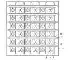
図7に、図2の電子放出素子を用いた電子源の構成例を模式的に示す。図中、11は基板、12は下配線、12aは下配線12の焼成前の導電層前駆体パターン、13は絶縁層、13aは絶縁層13の焼成前の誘電層前駆体パターン、14は上配線である。本例の電子源は、基板11上に、複数の電子放出素子をマトリクス状に配線接続してなり、各電子放出素子の構成は図2と同様である。図7の電子源は、一対の素子電極2,3を有する電子放出素子をX方向及びY方向に行列状に複数個配し、同じ行に配された複数の電子放出素子の素子電極の一方2を、X方向の上配線14に共通に接続し、同じ列に配された複数の電子放出素子の素子電極の他方3を、Y方向の下配線12に共通に接続したものも挙げられる。これは、いわゆる単純マトリクス配置である。 FIG. 7 schematically shows a configuration example of an electron source using the electron-emitting device of FIG. In the figure, 11 is a substrate, 12 is a lower wiring, 12a is a conductive layer precursor pattern before firing the
本発明の電子源の製造方法においては、下配線12と絶縁層13とを導電体ペーストと誘電体ペーストを用いてそれぞれパターニングした後、同時に焼成する。図7の電子源の製造工程を図3〜図7を用いて説明する。 In the method for manufacturing an electron source of the present invention, the
絶縁性の基板11を洗剤、純水及び有機溶剤により十分に洗浄後、一般的な真空蒸着技術、フォトリソグラフィ技術により、素子電極2,3を形成する(図3)。 After the insulating
基板1としては、石英ガラス、Na等の不純物含有量を減少させたガラス、青板ガラス、青板ガラスにスパッタ法等によりSiO2を積層した積層体、アルミナ等のセラミックス及びSi基板等を用いることができる。As the
素子電極2,3の材料としては、一般的導体材料を用いることができる。これは例えばNi,Cr,Au,Mo,W,Pt,Ti,Al,Cu,Pd等の金属或いは合金及びPd,Ag,Au,RuO2,Pd−Ag等の金属或いは金属酸化物とガラス等から構成される印刷導体、In2O3−SnO2等の透明導電体及びポリシリコン等の半導体材料等から適宜選択することができる。As a material for the
次いで、前記した本発明の積層体の形成方法により、先ず、下配線12を導電体ペーストを用いてパターニングして導電層前駆体パターン12aを形成し(図4)、さらに、これと交差して絶縁層13を誘電体ペーストを用いてパターニングして誘電層前駆体パターン13aを形成し(図5)、同時に焼成して下配線12と絶縁層13を得る。 Next, according to the method for forming a laminated body of the present invention, first, the
絶縁層13上に上配線14を形成する(図6)。上配線14の形成方法としては特に限定されないが、例えば下配線12と同様に導電体ペーストを用いた方法や、通常の真空蒸着法、印刷法、スパッタ法等を用いても良い。 An
次いで、素子電極2,3間を連絡する導電性膜4を形成する。 Next, a
導電性膜4としては、Ni、Au、PdO、Pd、Pt等の導電材料をRs(シート抵抗)が1×10²〜1×10⁷Ω/□の抵抗値を示す膜厚で形成したものが好ましく用いられる。尚Rsは、厚さがt、幅がwで長さがlの膜の長さ方向に測定した抵抗Rを、R=Rs(l/w)とおいたときに現れる値で、抵抗率をρとすればRs=ρ/tである。上記抵抗値を示す膜厚はおよそ5nm〜50nmの範囲にある。As the
導電性膜4の具体的な形成方法としては、例えば、基板11上に設けられた素子電極2と素子電極3との間に、有機金属溶液を塗布して乾燥することにより、有機金属膜を形成する。尚、有機金属溶液とは、前記導電性膜材料のPd、Ni、Au、Pt等の金属を主元素とする有機金属化合物の溶液である。この後、有機金属膜を加熱焼成処理し、リフトオフ、エッチング等によりパターニングし、導電性膜4を形成する。また、真空蒸着法、スパッタ法、CVD法、分散塗布法、ディッピング法、スピンナー法、インクジェット法等によって形成することも可能である。 As a specific method for forming the
続いて、素子電極2,3間にフォーミングと呼ばれる通電処理を、不図示の電源によりパルス状電圧或いは、昇電圧の印加により行い、導電性膜4の一部に間隙を形成する。尚、フォーミング処理は、適当な減圧雰囲気下にて行われることが好ましい。 Subsequently, an energization process called forming is performed between the
フォーミングが終了した素子に活性化処理を施す。活性化処理は、炭素化合物ガスを含む雰囲気の適当な真空度のもとで、素子電極2,3間に電圧を印加することで行い、この処理により、雰囲気中に存在する炭素化合物から、炭素及び/または炭素化合物を主成分とするカーボン膜が導電性膜4上に堆積され、電子放出特性の向上が図られる。 An activation process is performed on the element that has been formed. The activation treatment is performed by applying a voltage between the
活性化工程に用いる適当な炭素化合物としては、アルカン、アルケン、アルキンの脂肪族炭化水素類、芳香族炭化水素類、アルコール類、アルデヒド類、ケトン類、アミン類、フェノール、カルボン、スルホン酸等の有機酸類等を挙げることができ、具体的には、メタン、エタン、プロパンなどCnH2n+2で表される飽和炭化水素、エチレン、プロピレンなどCnH2n等の組成式で表される不飽和炭化水素、ベンゼン、トルエン、メタノール、エタノール、ホルムアルデヒド、アセトアルデヒド、アセトン、メチルエチルケトン、メチルアミン、エチルアミン、フェノール、ベンゾニトリル、トルニトリル、蟻酸、酢酸、プロピオン酸等或いはこれらの混合物を使用できる。Suitable carbon compounds used in the activation step include alkanes, alkenes, alkyne aliphatic hydrocarbons, aromatic hydrocarbons, alcohols, aldehydes, ketones, amines, phenols, carboxylic acids, sulfonic acids, etc. organic acids can be exemplified, specifically, represented methane, ethane, Cn H2n + 2 represented by a saturated hydrocarbon such as propane, ethylene, a composition formula such as propylene Cn H2n such Unsaturated hydrocarbons, benzene, toluene, methanol, ethanol, formaldehyde, acetaldehyde, acetone, methyl ethyl ketone, methylamine, ethylamine, phenol, benzonitrile, tolunitrile, formic acid, acetic acid, propionic acid, or a mixture thereof can be used.
以上のようにして、図7に示される電子源が作製される。 As described above, the electron source shown in FIG. 7 is manufactured.
本発明による電子源は、該電子源の電子放出素子から放出された電子の照射によって発光する発光部材を備えた画像形成部材と組み合わせて画像表示装置を構成することができる。画像形成部材として、電子によって可視光を発光する蛍光体を有するものを用いれば、テレビやコンピューターディスプレイとして用いられる表示パネルとすることができる。また、画像形成部材として、感光体ドラムを用い、電子線の照射によりこの感光体ドラムに形成される潜像をトナーを用いて現像できるようにすれば、コピー機やプリンターとすることができる。 The electron source according to the present invention can constitute an image display device in combination with an image forming member provided with a light emitting member that emits light by irradiation of electrons emitted from the electron emitting element of the electron source. If an image forming member having a phosphor that emits visible light by electrons is used, a display panel used as a television or a computer display can be obtained. Further, if a photosensitive drum is used as an image forming member and a latent image formed on the photosensitive drum by electron beam irradiation can be developed using toner, a copying machine or a printer can be obtained.
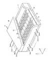
図7に示した単純マトリクス配置の電子源を用いた画像表示装置の一例について、図8を用いて説明する。図8は、本発明の画像表示装置の表示パネルの一部を切り欠いて示す模式図である。 An example of an image display apparatus using the electron source having the simple matrix arrangement shown in FIG. 7 will be described with reference to FIG. FIG. 8 is a schematic view in which a part of the display panel of the image display apparatus of the present invention is cut away.
図8において、15は図1に示した電子放出素子、16はリアプレート、18はガラス基板からなるフェースプレートで、フェースプレート18の内面には蛍光膜19とメタルバック20等が形成されている。17は支持枠、21は高圧電源である。リアプレート16、支持枠17及びフェースプレート18を、例えば10-5Pa程度の真空雰囲気中にて、封着して、外囲器が構成される。尚、電子源基板11が十分な強度を有する場合には、リアプレート16を用いず、該電子源基板11と支持枠17とを直接接着してもかまわない。In FIG. 8, 15 is the electron-emitting device shown in FIG. 1, 16 is a rear plate, 18 is a face plate made of a glass substrate, and a
また、フェースプレート18と電子源基板11との間に、スペーサーと呼ばれる不図示の支持体を設置することにより、大面積パネルの場合にも大気圧に対して十分な強度を持つ外囲器を構成することもできる。 In addition, by installing a support body (not shown) called a spacer between the
さらに、封着後の外囲器内の真空度を維持するために、封着の前後においてゲッター処理を行うことが好ましい。 Furthermore, in order to maintain the degree of vacuum in the envelope after sealing, it is preferable to perform a getter process before and after sealing.
(実施例1)
図3〜図7の工程に従って、電子源を作製した。Example 1
An electron source was fabricated according to the steps of FIGS.
ガラス製の基板11上にスパッタ成膜法によりPt/Ti膜を30nm/10nmの厚さで形成し、所望のパターンでレジストを形成後、ミリング法により不要な部分をエッチングし、縦×横=300μm×50μmの素子電極2と95μm×100μmの素子電極3を10μmの間隔をあけて対向して設置した(図3)。本電極は縦×横=600μm×200μmピッチで、それぞれ768×3840対形成した。 A Pt / Ti film having a thickness of 30 nm / 10 nm is formed on a
次に、SUS#200のスクリーン版を用いて電極作製済みの基板11上にAgの感光性樹脂ペースト(導電体ペースト)をスクリーン印刷法で塗布し、100℃で15分ほど保持し、乾燥させた。塗膜は乾燥後の膜厚が10μmであった。該Agの感光性樹脂ペースト膜の露光、現像を行い50μmの線幅に形成し、導電層前駆体パターン12aを形成した(図4)。 Next, an Ag photosensitive resin paste (conductor paste) is applied by screen printing on the
次にSUS#145のスクリーン版を用いて該基板11上にPbO系ガラスの感光性樹脂ペースト(誘電体ペースト)を塗布し、90℃で15分ほど保持し、乾燥させた。塗膜は基板11上から測定して35μm程度である。膜厚を稼ぐためにPbO系ガラスの感光性樹脂ペースト(誘電体ペースト)をSUS#200のスクリーン版を用いてもう一度塗布、乾燥を行い、トータル50μmの乾燥膜厚を得た。PbO系の感光性樹脂ペーストを導電層前駆体パターン12aと直交するようなストライプパターンで520μm幅に露光、現像を実施し、誘電層前駆体パターン13aを形成した。該誘電層前駆体パターン13aには、幅方向のセンターに100μm角の貫通孔が形成されていて貫通孔には電極2が露出している(図5)。 Next, a PbO-based glass photosensitive resin paste (dielectric paste) was applied onto the
こうして形成された基板11を焼成炉に投入し、10℃/分の昇温レートで420℃まで昇温し、この温度で20分間保持した後、10℃/分の昇温レートで500℃まで昇温し、10分間保持した。その後、室温まで40分で降下させ、下配線12と絶縁層13を得た。 The
本実施例において用いたPbO系の誘電体ペーストのガラス微粒子の軟化点は510℃、焼結開始温度は480℃、樹脂成分の分解温度は400℃、Agの導電体ペーストの樹脂成分の分解温度は400℃である。さらに、形成された絶縁層13上にストライプパターンに沿って、スクリーン印刷によって幅300μmのAgストライプパターンを印刷し、乾燥、焼成して上配線14を形成し、配線基板を得た(図6)。 The softening point of the glass particles of the PbO-based dielectric paste used in this example is 510 ° C., the sintering start temperature is 480 ° C., the decomposition temperature of the resin component is 400 ° C., and the decomposition temperature of the resin component of the Ag conductive paste. Is 400 ° C. Further, an Ag stripe pattern having a width of 300 μm was printed by screen printing along the stripe pattern on the formed insulating
以上のように作製された配線基板に前述のようにして、素子電極2、3間に、電子放出部を有する導電性膜4を形成して、図7に示される電子源を作製した。 As described above, the
本実施例で作製された電子源は、下配線12と絶縁層13とをその焼成工程を分けて形成した従来の場合に比べて、下配線12と上配線14との間での絶縁性能はより良好であり、また、上下配線の材料としてAgを用いたが、素子電極2、3付近で検出されるAgの量もより少なかった。 The electron source manufactured in this example has an insulation performance between the
また、本実施例で作製された電子源を用いた画像表示装置においても、表示性能の良好な信頼性の一層向上されたものであった。 Also in the image display apparatus using the electron source manufactured in this example, the display performance was excellent and the reliability was further improved.
(実施例2)
実施例1と同様に基板11上に素子電極2,3を形成した後、SUS#400カレンダー加工のスクリーン版を用いて電極作製済みのガラス基板上にAuペースト(エチルセルソース樹脂を樹脂成分として使用)を線幅80μmでスクリーン印刷法で塗布し、100℃で10分ほど保持し乾燥させて導電層前駆体パターン12aを形成した(図4)。塗膜は乾燥後の膜厚が13μmであった。(Example 2)
After forming the
次にSUS#145のスクリーン版を用いて該基板11上にBiO系ガラスの感光性樹脂ペースト(誘電体ペースト)を塗布し、90℃で15分ほど保持し乾燥させた。塗膜は基板11上から測定して35μm程度であった。膜厚を稼ぐためにBiO系ガラスの感光性樹脂ペースト(誘電体ペースト)をSUS#200のスクリーン版を用いてもう一度塗布し、乾燥させてトータル50μmの乾燥膜厚を得た。上記感光性樹脂ペースト(誘電体ペースト)を導電層前駆体パターン12aと直交するようなストライプパターンで520μm幅に露光、現像を実施し、誘電層前駆体パターン13aを形成した(図5)。該誘電層前駆体パターン13bには、幅方向のセンターに100μm角の貫通孔が形成されていて貫通孔には素子電極2が露出している。 Next, using a screen plate of SUS # 145, a photosensitive resin paste (dielectric paste) of BiO-based glass was applied onto the
こうして形成された基板を焼成炉に投入し、10℃/分の昇温レートで410℃まで昇温し、この温度で20分間保持した。次に、10℃/分の昇温レートで490℃まで昇温し10分間保持した。その後、室温まで40分で降下させ、下配線12と絶縁層13を得た。 The substrate thus formed was put into a firing furnace, heated to 410 ° C. at a temperature rising rate of 10 ° C./min, and held at this temperature for 20 minutes. Next, it heated up to 490 degreeC with the temperature increase rate of 10 degree-C / min, and hold | maintained for 10 minutes. Thereafter, the temperature was lowered to room temperature in 40 minutes, and the
本実施例において用いたBiO系の誘電体ペーストのガラス微粒子の軟化点は500℃、焼結開始温度は470℃、樹脂成分の分解温度は400℃であり、Auペーストの樹脂成分の分解温度は360℃である。さらに、形成された絶縁層13上にストライプパターンに沿って、スクリーン印刷によって幅300μmのAgストライプパターンを印刷し、乾燥後、焼成して上配線14を形成し、配線基板を得た(図6)。 The softening point of the glass particles of the BiO-based dielectric paste used in this example is 500 ° C., the sintering start temperature is 470 ° C., the decomposition temperature of the resin component is 400 ° C., and the decomposition temperature of the resin component of the Au paste is 360 ° C. Further, an Ag stripe pattern having a width of 300 μm was printed along the stripe pattern on the formed insulating
以上のように作製された配線基板に前述のようにして、素子電極2、3間に、電子放出部を有する導電性膜4を形成して、図7に示される電子源を作製した。 As described above, the
本実施例で作製された電子源においても、下配線12と絶縁層13とをその焼成工程を分けて形成した従来の場合に比べて、下配線12と上配線14との間での絶縁性能はより良好であった。 Also in the electron source manufactured in this example, the insulation performance between the
また、本実施例で作製された電子源を用いた画像表示装置においても、表示性能の良好な信頼性の一層向上されたものであった。 Also in the image display apparatus using the electron source manufactured in this example, the display performance was excellent and the reliability was further improved.
1 基板
2,3 素子電極
4 導電性膜
5 電子放出部
11 基板
12 下配線
12a 導電層前駆体パターン
13 絶縁層
13a 絶縁層前駆体パターン
14 上配線
15 電子放出素子
16 リアプレート
17 支持枠
18 フェースプレート
19 蛍光膜
20 メタルバック
21 高圧電源
91 基板
92 感光性ペースト
93 マスク
94 露光部
95 配線パターンDESCRIPTION OF
Claims (5)
Translated fromJapanese少なくとも樹脂成分とガラス微粒子とからなる誘電体ペーストを用いて、上記導電層前駆体パターンの少なくとも一部を覆う誘電層前駆体パターンを形成する工程と、
上記導電層前駆体パターンと誘電層前駆体パターンとを同時に焼成する焼成工程とを有する、少なくとも一部で導電層と誘電層とが積層する積層体の形成方法であって、
上記焼成工程において、焼成温度を、上記導電体ペーストの樹脂成分の分解温度以上及び誘電体ペーストの樹脂成分の分解温度以上であって、誘電体ペーストのガラス微粒子の焼結開始温度未満の温度領域にて所定の時間保持した後、
該ガラス微粒子の焼結開始温度以上、軟化点未満の温度領域にて焼成を行うことを特徴とする積層体の形成方法。Forming a conductive layer precursor pattern on a substrate using a conductive paste comprising at least a resin component, conductive fine particles and glass fine particles;
Forming a dielectric layer precursor pattern covering at least part of the conductive layer precursor pattern using a dielectric paste comprising at least a resin component and glass fine particles;
A method of forming a laminate in which at least a portion of the conductive layer and the dielectric layer are laminated, including a firing step of firing the conductive layer precursor pattern and the dielectric layer precursor pattern at the same time,
In the firing step, the firing temperature, there is the decomposition temperature or more of the resin component of the decomposition temperature or more and the dielectric paste of the resin component of the conductivepaste, the temperature region of below the sintering initiation temperature of the glass particles of the dielectric paste After holding for a predetermined time at
A method for forming a laminate, comprising firing at a temperature range from the sintering start temperature of the glass fine particles to less than the softening point.
Priority Applications (4)
| Application Number | Priority Date | Filing Date | Title |
|---|---|---|---|
| JP2004251412AJP4508785B2 (en) | 2004-08-31 | 2004-08-31 | LAMINATE FORMATION METHOD, ELECTRON SOURCE USING SAME, AND IMAGE DISPLAY DEVICE MANUFACTURING METHOD |
| US11/212,639US7470554B2 (en) | 2004-08-31 | 2005-08-29 | Forming method of stacking structure and manufacturing method of electron source and image display apparatus using such method |
| KR1020050079188AKR100740179B1 (en) | 2004-08-31 | 2005-08-29 | Forming method of stacking structure and manufacturing method of electron source and image display apparatus using such method |
| CNB2005100990055ACN100459015C (en) | 2004-08-31 | 2005-08-31 | Forming method of stacking structure and manufacturing method of electron source and image display apparatus using such method |
Applications Claiming Priority (1)
| Application Number | Priority Date | Filing Date | Title |
|---|---|---|---|
| JP2004251412AJP4508785B2 (en) | 2004-08-31 | 2004-08-31 | LAMINATE FORMATION METHOD, ELECTRON SOURCE USING SAME, AND IMAGE DISPLAY DEVICE MANUFACTURING METHOD |
Publications (2)
| Publication Number | Publication Date |
|---|---|
| JP2006073208A JP2006073208A (en) | 2006-03-16 |
| JP4508785B2true JP4508785B2 (en) | 2010-07-21 |
Family
ID=35943901
Family Applications (1)
| Application Number | Title | Priority Date | Filing Date |
|---|---|---|---|
| JP2004251412AExpired - Fee RelatedJP4508785B2 (en) | 2004-08-31 | 2004-08-31 | LAMINATE FORMATION METHOD, ELECTRON SOURCE USING SAME, AND IMAGE DISPLAY DEVICE MANUFACTURING METHOD |
Country Status (4)
| Country | Link |
|---|---|
| US (1) | US7470554B2 (en) |
| JP (1) | JP4508785B2 (en) |
| KR (1) | KR100740179B1 (en) |
| CN (1) | CN100459015C (en) |
Families Citing this family (3)
| Publication number | Priority date | Publication date | Assignee | Title |
|---|---|---|---|---|
| KR100922810B1 (en)* | 2007-12-11 | 2009-10-21 | 주식회사 잉크테크 | Manufacturing method of blackening conductive pattern |
| CN102804398A (en)* | 2009-06-10 | 2012-11-28 | 旭硝子株式会社 | Method of producing solar cell module |
| KR102584993B1 (en)* | 2018-02-08 | 2023-10-05 | 삼성전기주식회사 | Capacitor component and method of manufacturing the same |
Family Cites Families (11)
| Publication number | Priority date | Publication date | Assignee | Title |
|---|---|---|---|---|
| JPS594095A (en)* | 1982-06-30 | 1984-01-10 | 株式会社日立製作所 | Method of producing hybrid integrated circuit |
| JP3360378B2 (en)* | 1993-11-09 | 2002-12-24 | 東レ株式会社 | Method of forming pattern on ceramic green sheet |
| JPH11135904A (en)* | 1997-08-29 | 1999-05-21 | Dainippon Printing Co Ltd | Thick film electrode |
| JP2000311600A (en)* | 1999-02-23 | 2000-11-07 | Canon Inc | Electron source, image forming apparatus, method of manufacturing wiring board, and electron source, image forming apparatus, and wiring board using the manufacturing method |
| JP3397738B2 (en)* | 1999-02-25 | 2003-04-21 | キヤノン株式会社 | Electron source and image forming apparatus |
| JP3611503B2 (en)* | 1999-07-21 | 2005-01-19 | シャープ株式会社 | Electron source and manufacturing method thereof |
| KR100891240B1 (en)* | 2000-08-30 | 2009-04-01 | 파나소닉 주식회사 | Plasma display display device and manufacturing method thereof |
| JP2002198626A (en)* | 2000-12-27 | 2002-07-12 | Kyocera Corp | Method for manufacturing low-temperature fired ceramic circuit board |
| JP4366054B2 (en)* | 2001-08-03 | 2009-11-18 | キヤノン株式会社 | Matrix wiring manufacturing method, electron source, and image forming apparatus manufacturing method |
| US6653232B2 (en)* | 2001-08-03 | 2003-11-25 | Canon Kabushiki Kaisha | Method of manufacturing member pattern and method of manufacturing wiring, circuit substrate, electron source, and image-forming apparatus |
| JP4646468B2 (en)* | 2001-09-25 | 2011-03-09 | 京セラ株式会社 | Composition for through conductor |
- 2004
- 2004-08-31JPJP2004251412Apatent/JP4508785B2/ennot_activeExpired - Fee Related
- 2005
- 2005-08-29KRKR1020050079188Apatent/KR100740179B1/ennot_activeExpired - Fee Related
- 2005-08-29USUS11/212,639patent/US7470554B2/ennot_activeExpired - Fee Related
- 2005-08-31CNCNB2005100990055Apatent/CN100459015C/ennot_activeExpired - Fee Related
Also Published As
| Publication number | Publication date |
|---|---|
| KR20060050734A (en) | 2006-05-19 |
| JP2006073208A (en) | 2006-03-16 |
| CN100459015C (en) | 2009-02-04 |
| US7470554B2 (en) | 2008-12-30 |
| CN1763888A (en) | 2006-04-26 |
| KR100740179B1 (en) | 2007-07-16 |
| US20060046474A1 (en) | 2006-03-02 |
Similar Documents
| Publication | Publication Date | Title |
|---|---|---|
| US8013509B2 (en) | Electron-emitting device, electron source, and image display apparatus, and method for manufacturing the same | |
| JP4920925B2 (en) | ELECTRON EMITTING ELEMENT, ELECTRON SOURCE USING SAME, IMAGE DISPLAY DEVICE, INFORMATION DISPLAY REPRODUCING DEVICE, AND ITS MANUFACTURING METHOD | |
| US7298079B2 (en) | Electron source and an image display device including the electron source | |
| JP3703448B2 (en) | Electron emitting device, electron source substrate, display device, and manufacturing method of electron emitting device | |
| JP4508785B2 (en) | LAMINATE FORMATION METHOD, ELECTRON SOURCE USING SAME, AND IMAGE DISPLAY DEVICE MANUFACTURING METHOD | |
| US8269210B2 (en) | Cathode assembly containing an ultraviolet light-blocking dielectric layer | |
| JP2007103346A (en) | ELECTRON EMITTING ELEMENT, ELECTRON EMITTING DISPLAY DEVICE AND MANUFACTURING METHOD THEREOF | |
| US7807334B2 (en) | Substrate having fine line, electron source and image display apparatus | |
| EP2120245A1 (en) | Electron emitter and image display apparatus | |
| US20050266589A1 (en) | Formation method of electroconductive pattern, and production method of electron-emitting device, electron source, and image display apparatus using this | |
| JP2006215533A (en) | Flat panel display device and manufacturing method thereof | |
| JP4227601B2 (en) | Method for forming conductive pattern, electron-emitting device using the same, electron source, and method for manufacturing image display device | |
| JP2004253236A (en) | Manufacturing method of cold cathode display and cold cathode display | |
| KR100559539B1 (en) | Method of manufacturing member pattern, method of manufacturing wiring structure, method of manufacturing electron source, and method of manufacturing image display device | |
| JP3848228B2 (en) | Wiring device manufacturing method, electron source substrate manufacturing method, and image display device manufacturing method | |
| JP2010067387A (en) | Electron source, and image display apparatus | |
| JP4818802B2 (en) | Manufacturing method of electron emission source | |
| JP3880551B2 (en) | Wiring structure manufacturing method, electron source manufacturing method, and image display device manufacturing method | |
| JP2010009965A (en) | Electron-emitting element, its manufacturing method, electron source, and image display device | |
| JP2006134592A (en) | Electron emitting device, electron source, and manufacturing method of image forming apparatus | |
| HK1149848A (en) | Cathode assembly containing an ultraviolet light-blocking dielectric layer | |
| JP2008077960A (en) | Electron source and manufacturing method thereof | |
| JP2006019248A (en) | Electron emitting device, electron source, image display device, and method for manufacturing electron emitting device | |
| KR20050104548A (en) | Fed, and manufacturing method thereof | |
| KR20050096524A (en) | Electron emission device having layer for preventing diffusion of auxiliary electrode and method for forming the same |
Legal Events
| Date | Code | Title | Description |
|---|---|---|---|
| A621 | Written request for application examination | Free format text:JAPANESE INTERMEDIATE CODE: A621 Effective date:20070823 | |
| A977 | Report on retrieval | Free format text:JAPANESE INTERMEDIATE CODE: A971007 Effective date:20091016 | |
| A131 | Notification of reasons for refusal | Free format text:JAPANESE INTERMEDIATE CODE: A131 Effective date:20091104 | |
| A521 | Request for written amendment filed | Free format text:JAPANESE INTERMEDIATE CODE: A523 Effective date:20091221 | |
| A131 | Notification of reasons for refusal | Free format text:JAPANESE INTERMEDIATE CODE: A131 Effective date:20100202 | |
| A521 | Request for written amendment filed | Free format text:JAPANESE INTERMEDIATE CODE: A523 Effective date:20100215 | |
| TRDD | Decision of grant or rejection written | ||
| A01 | Written decision to grant a patent or to grant a registration (utility model) | Free format text:JAPANESE INTERMEDIATE CODE: A01 Effective date:20100420 | |
| A01 | Written decision to grant a patent or to grant a registration (utility model) | Free format text:JAPANESE INTERMEDIATE CODE: A01 | |
| A61 | First payment of annual fees (during grant procedure) | Free format text:JAPANESE INTERMEDIATE CODE: A61 Effective date:20100427 | |
| FPAY | Renewal fee payment (event date is renewal date of database) | Free format text:PAYMENT UNTIL: 20130514 Year of fee payment:3 | |
| R150 | Certificate of patent or registration of utility model | Free format text:JAPANESE INTERMEDIATE CODE: R150 | |
| FPAY | Renewal fee payment (event date is renewal date of database) | Free format text:PAYMENT UNTIL: 20140514 Year of fee payment:4 | |
| LAPS | Cancellation because of no payment of annual fees |