JP4507101B2 - Semiconductor memory device and manufacturing method thereof - Google Patents
Semiconductor memory device and manufacturing method thereofDownload PDFInfo
- Publication number
- JP4507101B2 JP4507101B2JP2005191257AJP2005191257AJP4507101B2JP 4507101 B2JP4507101 B2JP 4507101B2JP 2005191257 AJP2005191257 AJP 2005191257AJP 2005191257 AJP2005191257 AJP 2005191257AJP 4507101 B2JP4507101 B2JP 4507101B2
- Authority
- JP
- Japan
- Prior art keywords
- electrode
- memory device
- internal
- semiconductor memory
- internal electrode
- Prior art date
- Legal status (The legal status is an assumption and is not a legal conclusion. Google has not performed a legal analysis and makes no representation as to the accuracy of the status listed.)
- Expired - Fee Related
Links
Images


Classifications
- H—ELECTRICITY
- H01—ELECTRIC ELEMENTS
- H01L—SEMICONDUCTOR DEVICES NOT COVERED BY CLASS H10
- H01L21/00—Processes or apparatus adapted for the manufacture or treatment of semiconductor or solid state devices or of parts thereof
- H01L21/67—Apparatus specially adapted for handling semiconductor or electric solid state devices during manufacture or treatment thereof; Apparatus specially adapted for handling wafers during manufacture or treatment of semiconductor or electric solid state devices or components ; Apparatus not specifically provided for elsewhere
- H01L21/683—Apparatus specially adapted for handling semiconductor or electric solid state devices during manufacture or treatment thereof; Apparatus specially adapted for handling wafers during manufacture or treatment of semiconductor or electric solid state devices or components ; Apparatus not specifically provided for elsewhere for supporting or gripping
- H01L21/6835—Apparatus specially adapted for handling semiconductor or electric solid state devices during manufacture or treatment thereof; Apparatus specially adapted for handling wafers during manufacture or treatment of semiconductor or electric solid state devices or components ; Apparatus not specifically provided for elsewhere for supporting or gripping using temporarily an auxiliary support
- G—PHYSICS
- G11—INFORMATION STORAGE
- G11C—STATIC STORES
- G11C5/00—Details of stores covered by group G11C11/00
- G11C5/02—Disposition of storage elements, e.g. in the form of a matrix array
- G—PHYSICS
- G11—INFORMATION STORAGE
- G11C—STATIC STORES
- G11C5/00—Details of stores covered by group G11C11/00
- G11C5/02—Disposition of storage elements, e.g. in the form of a matrix array
- G11C5/025—Geometric lay-out considerations of storage- and peripheral-blocks in a semiconductor storage device
- H—ELECTRICITY
- H01—ELECTRIC ELEMENTS
- H01L—SEMICONDUCTOR DEVICES NOT COVERED BY CLASS H10
- H01L24/00—Arrangements for connecting or disconnecting semiconductor or solid-state bodies; Methods or apparatus related thereto
- H01L24/93—Batch processes
- H01L24/95—Batch processes at chip-level, i.e. with connecting carried out on a plurality of singulated devices, i.e. on diced chips
- H01L24/97—Batch processes at chip-level, i.e. with connecting carried out on a plurality of singulated devices, i.e. on diced chips the devices being connected to a common substrate, e.g. interposer, said common substrate being separable into individual assemblies after connecting
- H—ELECTRICITY
- H01—ELECTRIC ELEMENTS
- H01L—SEMICONDUCTOR DEVICES NOT COVERED BY CLASS H10
- H01L25/00—Assemblies consisting of a plurality of semiconductor or other solid state devices
- H01L25/03—Assemblies consisting of a plurality of semiconductor or other solid state devices all the devices being of a type provided for in a single subclass of subclasses H10B, H10D, H10F, H10H, H10K or H10N, e.g. assemblies of rectifier diodes
- H01L25/04—Assemblies consisting of a plurality of semiconductor or other solid state devices all the devices being of a type provided for in a single subclass of subclasses H10B, H10D, H10F, H10H, H10K or H10N, e.g. assemblies of rectifier diodes the devices not having separate containers
- H01L25/065—Assemblies consisting of a plurality of semiconductor or other solid state devices all the devices being of a type provided for in a single subclass of subclasses H10B, H10D, H10F, H10H, H10K or H10N, e.g. assemblies of rectifier diodes the devices not having separate containers the devices being of a type provided for in group H10D89/00
- H01L25/0657—Stacked arrangements of devices
- H—ELECTRICITY
- H01—ELECTRIC ELEMENTS
- H01L—SEMICONDUCTOR DEVICES NOT COVERED BY CLASS H10
- H01L25/00—Assemblies consisting of a plurality of semiconductor or other solid state devices
- H01L25/50—Multistep manufacturing processes of assemblies consisting of devices, the devices being individual devices of subclass H10D or integrated devices of class H10
- H—ELECTRICITY
- H01—ELECTRIC ELEMENTS
- H01L—SEMICONDUCTOR DEVICES NOT COVERED BY CLASS H10
- H01L2224/00—Indexing scheme for arrangements for connecting or disconnecting semiconductor or solid-state bodies and methods related thereto as covered by H01L24/00
- H01L2224/01—Means for bonding being attached to, or being formed on, the surface to be connected, e.g. chip-to-package, die-attach, "first-level" interconnects; Manufacturing methods related thereto
- H01L2224/02—Bonding areas; Manufacturing methods related thereto
- H01L2224/04—Structure, shape, material or disposition of the bonding areas prior to the connecting process
- H01L2224/05—Structure, shape, material or disposition of the bonding areas prior to the connecting process of an individual bonding area
- H01L2224/0554—External layer
- H01L2224/05573—Single external layer
- H—ELECTRICITY
- H01—ELECTRIC ELEMENTS
- H01L—SEMICONDUCTOR DEVICES NOT COVERED BY CLASS H10
- H01L2224/00—Indexing scheme for arrangements for connecting or disconnecting semiconductor or solid-state bodies and methods related thereto as covered by H01L24/00
- H01L2224/01—Means for bonding being attached to, or being formed on, the surface to be connected, e.g. chip-to-package, die-attach, "first-level" interconnects; Manufacturing methods related thereto
- H01L2224/02—Bonding areas; Manufacturing methods related thereto
- H01L2224/04—Structure, shape, material or disposition of the bonding areas prior to the connecting process
- H01L2224/06—Structure, shape, material or disposition of the bonding areas prior to the connecting process of a plurality of bonding areas
- H01L2224/061—Disposition
- H01L2224/0612—Layout
- H01L2224/0613—Square or rectangular array
- H01L2224/06131—Square or rectangular array being uniform, i.e. having a uniform pitch across the array
- H—ELECTRICITY
- H01—ELECTRIC ELEMENTS
- H01L—SEMICONDUCTOR DEVICES NOT COVERED BY CLASS H10
- H01L2224/00—Indexing scheme for arrangements for connecting or disconnecting semiconductor or solid-state bodies and methods related thereto as covered by H01L24/00
- H01L2224/01—Means for bonding being attached to, or being formed on, the surface to be connected, e.g. chip-to-package, die-attach, "first-level" interconnects; Manufacturing methods related thereto
- H01L2224/10—Bump connectors; Manufacturing methods related thereto
- H01L2224/12—Structure, shape, material or disposition of the bump connectors prior to the connecting process
- H01L2224/13—Structure, shape, material or disposition of the bump connectors prior to the connecting process of an individual bump connector
- H01L2224/13001—Core members of the bump connector
- H01L2224/1302—Disposition
- H01L2224/13025—Disposition the bump connector being disposed on a via connection of the semiconductor or solid-state body
- H—ELECTRICITY
- H01—ELECTRIC ELEMENTS
- H01L—SEMICONDUCTOR DEVICES NOT COVERED BY CLASS H10
- H01L2224/00—Indexing scheme for arrangements for connecting or disconnecting semiconductor or solid-state bodies and methods related thereto as covered by H01L24/00
- H01L2224/01—Means for bonding being attached to, or being formed on, the surface to be connected, e.g. chip-to-package, die-attach, "first-level" interconnects; Manufacturing methods related thereto
- H01L2224/10—Bump connectors; Manufacturing methods related thereto
- H01L2224/15—Structure, shape, material or disposition of the bump connectors after the connecting process
- H01L2224/16—Structure, shape, material or disposition of the bump connectors after the connecting process of an individual bump connector
- H01L2224/161—Disposition
- H01L2224/16135—Disposition the bump connector connecting between different semiconductor or solid-state bodies, i.e. chip-to-chip
- H01L2224/16145—Disposition the bump connector connecting between different semiconductor or solid-state bodies, i.e. chip-to-chip the bodies being stacked
- H—ELECTRICITY
- H01—ELECTRIC ELEMENTS
- H01L—SEMICONDUCTOR DEVICES NOT COVERED BY CLASS H10
- H01L2224/00—Indexing scheme for arrangements for connecting or disconnecting semiconductor or solid-state bodies and methods related thereto as covered by H01L24/00
- H01L2224/01—Means for bonding being attached to, or being formed on, the surface to be connected, e.g. chip-to-package, die-attach, "first-level" interconnects; Manufacturing methods related thereto
- H01L2224/10—Bump connectors; Manufacturing methods related thereto
- H01L2224/15—Structure, shape, material or disposition of the bump connectors after the connecting process
- H01L2224/16—Structure, shape, material or disposition of the bump connectors after the connecting process of an individual bump connector
- H01L2224/161—Disposition
- H01L2224/16151—Disposition the bump connector connecting between a semiconductor or solid-state body and an item not being a semiconductor or solid-state body, e.g. chip-to-substrate, chip-to-passive
- H01L2224/16221—Disposition the bump connector connecting between a semiconductor or solid-state body and an item not being a semiconductor or solid-state body, e.g. chip-to-substrate, chip-to-passive the body and the item being stacked
- H01L2224/16225—Disposition the bump connector connecting between a semiconductor or solid-state body and an item not being a semiconductor or solid-state body, e.g. chip-to-substrate, chip-to-passive the body and the item being stacked the item being non-metallic, e.g. insulating substrate with or without metallisation
- H—ELECTRICITY
- H01—ELECTRIC ELEMENTS
- H01L—SEMICONDUCTOR DEVICES NOT COVERED BY CLASS H10
- H01L2224/00—Indexing scheme for arrangements for connecting or disconnecting semiconductor or solid-state bodies and methods related thereto as covered by H01L24/00
- H01L2224/80—Methods for connecting semiconductor or other solid state bodies using means for bonding being attached to, or being formed on, the surface to be connected
- H01L2224/81—Methods for connecting semiconductor or other solid state bodies using means for bonding being attached to, or being formed on, the surface to be connected using a bump connector
- H01L2224/81001—Methods for connecting semiconductor or other solid state bodies using means for bonding being attached to, or being formed on, the surface to be connected using a bump connector involving a temporary auxiliary member not forming part of the bonding apparatus
- H01L2224/81005—Methods for connecting semiconductor or other solid state bodies using means for bonding being attached to, or being formed on, the surface to be connected using a bump connector involving a temporary auxiliary member not forming part of the bonding apparatus being a temporary or sacrificial substrate
- H—ELECTRICITY
- H01—ELECTRIC ELEMENTS
- H01L—SEMICONDUCTOR DEVICES NOT COVERED BY CLASS H10
- H01L2224/00—Indexing scheme for arrangements for connecting or disconnecting semiconductor or solid-state bodies and methods related thereto as covered by H01L24/00
- H01L2224/93—Batch processes
- H01L2224/94—Batch processes at wafer-level, i.e. with connecting carried out on a wafer comprising a plurality of undiced individual devices
- H—ELECTRICITY
- H01—ELECTRIC ELEMENTS
- H01L—SEMICONDUCTOR DEVICES NOT COVERED BY CLASS H10
- H01L2224/00—Indexing scheme for arrangements for connecting or disconnecting semiconductor or solid-state bodies and methods related thereto as covered by H01L24/00
- H01L2224/93—Batch processes
- H01L2224/95—Batch processes at chip-level, i.e. with connecting carried out on a plurality of singulated devices, i.e. on diced chips
- H01L2224/97—Batch processes at chip-level, i.e. with connecting carried out on a plurality of singulated devices, i.e. on diced chips the devices being connected to a common substrate, e.g. interposer, said common substrate being separable into individual assemblies after connecting
- H—ELECTRICITY
- H01—ELECTRIC ELEMENTS
- H01L—SEMICONDUCTOR DEVICES NOT COVERED BY CLASS H10
- H01L2225/00—Details relating to assemblies covered by the group H01L25/00 but not provided for in its subgroups
- H01L2225/03—All the devices being of a type provided for in the same main group of the same subclass of class H10, e.g. assemblies of rectifier diodes
- H01L2225/04—All the devices being of a type provided for in the same main group of the same subclass of class H10, e.g. assemblies of rectifier diodes the devices not having separate containers
- H01L2225/065—All the devices being of a type provided for in the same main group of the same subclass of class H10
- H01L2225/06503—Stacked arrangements of devices
- H01L2225/06513—Bump or bump-like direct electrical connections between devices, e.g. flip-chip connection, solder bumps
- H—ELECTRICITY
- H01—ELECTRIC ELEMENTS
- H01L—SEMICONDUCTOR DEVICES NOT COVERED BY CLASS H10
- H01L2225/00—Details relating to assemblies covered by the group H01L25/00 but not provided for in its subgroups
- H01L2225/03—All the devices being of a type provided for in the same main group of the same subclass of class H10, e.g. assemblies of rectifier diodes
- H01L2225/04—All the devices being of a type provided for in the same main group of the same subclass of class H10, e.g. assemblies of rectifier diodes the devices not having separate containers
- H01L2225/065—All the devices being of a type provided for in the same main group of the same subclass of class H10
- H01L2225/06503—Stacked arrangements of devices
- H01L2225/06517—Bump or bump-like direct electrical connections from device to substrate
- H—ELECTRICITY
- H01—ELECTRIC ELEMENTS
- H01L—SEMICONDUCTOR DEVICES NOT COVERED BY CLASS H10
- H01L2225/00—Details relating to assemblies covered by the group H01L25/00 but not provided for in its subgroups
- H01L2225/03—All the devices being of a type provided for in the same main group of the same subclass of class H10, e.g. assemblies of rectifier diodes
- H01L2225/04—All the devices being of a type provided for in the same main group of the same subclass of class H10, e.g. assemblies of rectifier diodes the devices not having separate containers
- H01L2225/065—All the devices being of a type provided for in the same main group of the same subclass of class H10
- H01L2225/06503—Stacked arrangements of devices
- H01L2225/06527—Special adaptation of electrical connections, e.g. rewiring, engineering changes, pressure contacts, layout
- H—ELECTRICITY
- H01—ELECTRIC ELEMENTS
- H01L—SEMICONDUCTOR DEVICES NOT COVERED BY CLASS H10
- H01L2225/00—Details relating to assemblies covered by the group H01L25/00 but not provided for in its subgroups
- H01L2225/03—All the devices being of a type provided for in the same main group of the same subclass of class H10, e.g. assemblies of rectifier diodes
- H01L2225/04—All the devices being of a type provided for in the same main group of the same subclass of class H10, e.g. assemblies of rectifier diodes the devices not having separate containers
- H01L2225/065—All the devices being of a type provided for in the same main group of the same subclass of class H10
- H01L2225/06503—Stacked arrangements of devices
- H01L2225/06541—Conductive via connections through the device, e.g. vertical interconnects, through silicon via [TSV]
- H—ELECTRICITY
- H01—ELECTRIC ELEMENTS
- H01L—SEMICONDUCTOR DEVICES NOT COVERED BY CLASS H10
- H01L2225/00—Details relating to assemblies covered by the group H01L25/00 but not provided for in its subgroups
- H01L2225/03—All the devices being of a type provided for in the same main group of the same subclass of class H10, e.g. assemblies of rectifier diodes
- H01L2225/04—All the devices being of a type provided for in the same main group of the same subclass of class H10, e.g. assemblies of rectifier diodes the devices not having separate containers
- H01L2225/065—All the devices being of a type provided for in the same main group of the same subclass of class H10
- H01L2225/06503—Stacked arrangements of devices
- H01L2225/06555—Geometry of the stack, e.g. form of the devices, geometry to facilitate stacking
- H—ELECTRICITY
- H01—ELECTRIC ELEMENTS
- H01L—SEMICONDUCTOR DEVICES NOT COVERED BY CLASS H10
- H01L2225/00—Details relating to assemblies covered by the group H01L25/00 but not provided for in its subgroups
- H01L2225/03—All the devices being of a type provided for in the same main group of the same subclass of class H10, e.g. assemblies of rectifier diodes
- H01L2225/04—All the devices being of a type provided for in the same main group of the same subclass of class H10, e.g. assemblies of rectifier diodes the devices not having separate containers
- H01L2225/065—All the devices being of a type provided for in the same main group of the same subclass of class H10
- H01L2225/06503—Stacked arrangements of devices
- H01L2225/06572—Auxiliary carrier between devices, the carrier having an electrical connection structure
- H—ELECTRICITY
- H01—ELECTRIC ELEMENTS
- H01L—SEMICONDUCTOR DEVICES NOT COVERED BY CLASS H10
- H01L2225/00—Details relating to assemblies covered by the group H01L25/00 but not provided for in its subgroups
- H01L2225/03—All the devices being of a type provided for in the same main group of the same subclass of class H10, e.g. assemblies of rectifier diodes
- H01L2225/04—All the devices being of a type provided for in the same main group of the same subclass of class H10, e.g. assemblies of rectifier diodes the devices not having separate containers
- H01L2225/065—All the devices being of a type provided for in the same main group of the same subclass of class H10
- H01L2225/06503—Stacked arrangements of devices
- H01L2225/06582—Housing for the assembly, e.g. chip scale package [CSP]
- H01L2225/06586—Housing with external bump or bump-like connectors
- H—ELECTRICITY
- H01—ELECTRIC ELEMENTS
- H01L—SEMICONDUCTOR DEVICES NOT COVERED BY CLASS H10
- H01L2225/00—Details relating to assemblies covered by the group H01L25/00 but not provided for in its subgroups
- H01L2225/03—All the devices being of a type provided for in the same main group of the same subclass of class H10, e.g. assemblies of rectifier diodes
- H01L2225/04—All the devices being of a type provided for in the same main group of the same subclass of class H10, e.g. assemblies of rectifier diodes the devices not having separate containers
- H01L2225/065—All the devices being of a type provided for in the same main group of the same subclass of class H10
- H01L2225/06503—Stacked arrangements of devices
- H01L2225/06596—Structural arrangements for testing
- H—ELECTRICITY
- H01—ELECTRIC ELEMENTS
- H01L—SEMICONDUCTOR DEVICES NOT COVERED BY CLASS H10
- H01L23/00—Details of semiconductor or other solid state devices
- H01L23/48—Arrangements for conducting electric current to or from the solid state body in operation, e.g. leads, terminal arrangements ; Selection of materials therefor
- H01L23/481—Internal lead connections, e.g. via connections, feedthrough structures
- H—ELECTRICITY
- H01—ELECTRIC ELEMENTS
- H01L—SEMICONDUCTOR DEVICES NOT COVERED BY CLASS H10
- H01L2924/00—Indexing scheme for arrangements or methods for connecting or disconnecting semiconductor or solid-state bodies as covered by H01L24/00
- H01L2924/0001—Technical content checked by a classifier
- H01L2924/00014—Technical content checked by a classifier the subject-matter covered by the group, the symbol of which is combined with the symbol of this group, being disclosed without further technical details
- H—ELECTRICITY
- H01—ELECTRIC ELEMENTS
- H01L—SEMICONDUCTOR DEVICES NOT COVERED BY CLASS H10
- H01L2924/00—Indexing scheme for arrangements or methods for connecting or disconnecting semiconductor or solid-state bodies as covered by H01L24/00
- H01L2924/15—Details of package parts other than the semiconductor or other solid state devices to be connected
- H01L2924/151—Die mounting substrate
- H01L2924/153—Connection portion
- H01L2924/1531—Connection portion the connection portion being formed only on the surface of the substrate opposite to the die mounting surface
- H01L2924/15311—Connection portion the connection portion being formed only on the surface of the substrate opposite to the die mounting surface being a ball array, e.g. BGA
- H—ELECTRICITY
- H01—ELECTRIC ELEMENTS
- H01L—SEMICONDUCTOR DEVICES NOT COVERED BY CLASS H10
- H01L2924/00—Indexing scheme for arrangements or methods for connecting or disconnecting semiconductor or solid-state bodies as covered by H01L24/00
- H01L2924/15—Details of package parts other than the semiconductor or other solid state devices to be connected
- H01L2924/151—Die mounting substrate
- H01L2924/153—Connection portion
- H01L2924/1532—Connection portion the connection portion being formed on the die mounting surface of the substrate
- H—ELECTRICITY
- H01—ELECTRIC ELEMENTS
- H01L—SEMICONDUCTOR DEVICES NOT COVERED BY CLASS H10
- H01L2924/00—Indexing scheme for arrangements or methods for connecting or disconnecting semiconductor or solid-state bodies as covered by H01L24/00
- H01L2924/15—Details of package parts other than the semiconductor or other solid state devices to be connected
- H01L2924/151—Die mounting substrate
- H01L2924/156—Material
- H01L2924/15786—Material with a principal constituent of the material being a non metallic, non metalloid inorganic material
- H01L2924/15787—Ceramics, e.g. crystalline carbides, nitrides or oxides
- H—ELECTRICITY
- H01—ELECTRIC ELEMENTS
- H01L—SEMICONDUCTOR DEVICES NOT COVERED BY CLASS H10
- H01L2924/00—Indexing scheme for arrangements or methods for connecting or disconnecting semiconductor or solid-state bodies as covered by H01L24/00
- H01L2924/15—Details of package parts other than the semiconductor or other solid state devices to be connected
- H01L2924/181—Encapsulation
- H—ELECTRICITY
- H01—ELECTRIC ELEMENTS
- H01L—SEMICONDUCTOR DEVICES NOT COVERED BY CLASS H10
- H01L2924/00—Indexing scheme for arrangements or methods for connecting or disconnecting semiconductor or solid-state bodies as covered by H01L24/00
- H01L2924/30—Technical effects
- H01L2924/301—Electrical effects
- H01L2924/30105—Capacitance
Landscapes
- Engineering & Computer Science (AREA)
- Microelectronics & Electronic Packaging (AREA)
- Power Engineering (AREA)
- Computer Hardware Design (AREA)
- Physics & Mathematics (AREA)
- Condensed Matter Physics & Semiconductors (AREA)
- General Physics & Mathematics (AREA)
- Manufacturing & Machinery (AREA)
- Semiconductor Memories (AREA)
Description
Translated fromJapanese本発明は半導体記憶装置及びその製造方法に関し、特に、メモリセルが形成されたコア部がインターフェース部とは別個に集積されるタイプの半導体記憶装置及びその製造方法に関する。 The present invention relates to a semiconductor memory device and a manufacturing method thereof, and more particularly to a semiconductor memory device of a type in which a core portion in which a memory cell is formed is integrated separately from an interface portion and a manufacturing method thereof.
DRAM(Dynamic Random Access Memory)に代表される半導体記憶装置の記憶容量は、近年ますます増大し、高速化も要求されている。記憶容量の増大は、これまで主にメモリセルの小型化とチップサイズの大型化によって達成されてきたが、メモリセルの小型化には一定の物理的限界があり、また、チップサイズの大型化は歩留まりの低下を招くとともに高速化を妨げるという問題がある。 In recent years, the storage capacity of semiconductor memory devices represented by DRAM (Dynamic Random Access Memory) has been increasing more and more, and higher speed has been demanded. Up to now, the increase in storage capacity has been achieved mainly by reducing the size of memory cells and increasing the chip size. However, there are certain physical limitations to the size reduction of memory cells, and the increase in chip size. However, there is a problem that the yield is lowered and the speeding up is hindered.
この問題を根本的に解決する方法として、メモリセルが形成されたコア部と、メモリセルに対する周辺回路が形成されたインターフェース部をそれぞれ別チップとする方法が提案されている(特許文献1参照)。この方法によれば、1つのインターフェースチップに対して複数個のコアチップを割り当てることが可能となることから、1チップ当たりのチップサイズを大幅に低減することが可能となる。このため、この方法によれば、高い歩留まりを確保しつつ、さらなる大容量化を実現できるものと期待されている。 As a method for fundamentally solving this problem, a method has been proposed in which a core part in which a memory cell is formed and an interface part in which a peripheral circuit for the memory cell is formed in separate chips (see Patent Document 1). . According to this method, since a plurality of core chips can be assigned to one interface chip, the chip size per chip can be greatly reduced. For this reason, according to this method, it is expected that further increase in capacity can be realized while ensuring a high yield.
しかも、コア部とインターフェース部を別チップとした場合、コアチップについてはメモリプロセスにて製造し、インターフェースチップについてはロジックプロセスにて製造することが可能である。一般的に、ロジックプロセスにて製造されたトランジスタは、メモリプロセスにて製造されたトランジスタに比べて高速動作が可能であるため、インターフェースチップをロジックプロセスにて製造すれば、従来に比べインターフェースチップ部の回路を高速に動作させる事が可能となり、結果的に、半導体記憶装置の高速化を達成することが可能となる。しかも、インターフェースチップの動作電圧を1V程度に下げることが可能となり、消費電力の低減を図ることも可能となる。 Moreover, when the core portion and the interface portion are separate chips, the core chip can be manufactured by a memory process, and the interface chip can be manufactured by a logic process. Generally, a transistor manufactured by a logic process can operate at a higher speed than a transistor manufactured by a memory process. This circuit can be operated at a high speed, and as a result, the semiconductor memory device can be speeded up. In addition, the operating voltage of the interface chip can be lowered to about 1 V, and the power consumption can be reduced.
図18は、従来の半導体記憶装置の構造を模式的に示す略断面図である。 FIG. 18 is a schematic cross-sectional view schematically showing the structure of a conventional semiconductor memory device.
図18に示すように、従来の半導体記憶装置は、インターポーザ基板10と、インターポーザ基板10の一方の面10aに搭載されたインターフェースチップ20と、インターフェースチップ20上に積層された複数(一例として4個)のコアチップ31〜34によって構成される。外部回路との信号の授受は、インターポーザ基板10の他方の面10bに設けられた外部端子11を介して行われ、インターフェースチップ20とコアチップ31〜34との間の信号の授受は、これらに設けられた内部端子40及び貫通電極41を介して行われる。この種の半導体記憶装置では、外部端子11を介して授受される信号の信号幅よりも、内部端子40を介して授受される信号の信号幅の方が大きく、これら信号幅の変換をインターフェースチップ20が行う。 As shown in FIG. 18, the conventional semiconductor memory device includes an
すなわち、外部回路より外部端子11を介して供給される信号(アドレス、コマンド、ライトデータなど)は、一旦インターフェースチップ20に供給され、インターフェースチップ20によって信号幅が拡大された後、コアチップ31〜34へと供給される。逆に、コアチップ31〜34より供給される信号(リードデータなど)は、一旦インターフェースチップ20に供給され、インターフェースチップ20によって信号幅を縮小された後、インターポーザ基板10の外部端子11を介して出力される。これにより、大幅な並列動作が可能であるが動作速度の遅いDRAMなどのメモリコアと、大幅な並列動作は困難であるが動作速度の速いCPUなどのロジック系回路との間のバンド幅を大幅に高めることが可能となる。
DRAMなどの半導体記憶装置は、同種の製品であっても、入出力データ幅の異なる複数の製品(×8品と×16品との違いなど)が存在したり、動作クロックの異なる複数の製品(200MHz品と×266MHz品との違いなど)が存在するなど、仕様の異なる数多くの製品が存在する。このような仕様の違いは、主としてインターフェースチップ20の回路構成によって実現されるのであるが、従来の半導体記憶装置では、インターポーザ基板10上にインターフェースチップ20及びコアチップ31〜34が一括搭載された構成を有していることから、積層完了後に仕様を変更することは不可能であり、このため、顧客のニーズに応じた機動的な生産を行うことは難しかった。 Even if semiconductor storage devices such as DRAMs are the same type of products, there are multiple products with different input / output data widths (difference between × 8 products and × 16 products, etc.) and multiple products with different operation clocks. There are many products with different specifications, such as a difference between a 200 MHz product and a × 266 MHz product. Such a difference in specifications is mainly realized by the circuit configuration of the
このような問題を解決するためには、インターフェースチップ20やコアチップ31〜34を積層せずにストックしておき、生産すべき半導体記憶装置の仕様が確定した段階で、ストックしておいたインターフェースチップ20やコアチップ31〜34を積層する方法が考えられる。しかしながら、この方法では、封止前のベアチップを多量にストックしておく必要があるため、長期間に亘りこれらが外部環境に晒される可能性がある。特に、コアチップは長期間外に亘り外部環境に晒されると不良が発生する可能性が高いため、ベアチップ状態のコアチップを多量にストックしておくと、最終製品である半導体記憶装置の信頼性低下を招くおそれがあった。 In order to solve such a problem, the
したがって、本発明は、信頼性の低下を抑制しつつ、複数のコアチップとインターフェースチップによって構成される半導体記憶装置の仕様変更を容易とすることを目的とする。 Therefore, an object of the present invention is to make it easy to change the specifications of a semiconductor memory device including a plurality of core chips and interface chips while suppressing a decrease in reliability.
本発明による半導体記憶装置は、第1の面に複数の第1の内部電極が形成され、前記第1の面と対向する第2の面に複数の第2の内部電極及び前記第2の内部電極よりも電極ピッチの広い複数の第3の内部電極が形成されたインターポーザチップと、前記インターポーザチップの前記第1の面側に搭載され、前記第1の内部電極に接続された複数のコアチップとを備え、前記インターポーザチップは、半導体基板と、前記半導体基板の少なくとも一方の面に形成された再配線層と、前記半導体基板に形成され、前記第1の内部電極の一部と前記第2の内部電極の一部とを接続する複数の第1の貫通電極と、前記半導体基板に形成され、前記第1の内部電極の他の一部と前記第3の内部電極の一部とを接続する複数の第2の貫通電極とを有しており、前記第1の貫通電極の電極ピッチは、前記第1の内部電極の電極ピッチ及び前記第2の内部電極の電極ピッチの少なくとも一方と実質的に等しいことを特徴とする。 In the semiconductor memory device according to the present invention, a plurality of first internal electrodes are formed on a first surface, and a plurality of second internal electrodes and the second internal electrode are formed on a second surface opposite to the first surface. An interposer chip in which a plurality of third internal electrodes having a wider electrode pitch than electrodes are formed; a plurality of core chips mounted on the first surface side of the interposer chip and connected to the first internal electrodes; The interposer chip includes a semiconductor substrate, a redistribution layer formed on at least one surface of the semiconductor substrate, a part of the first internal electrode formed on the semiconductor substrate, and the second A plurality of first through electrodes that connect a part of the internal electrodes, and another part of the first internal electrode that is formed on the semiconductor substrate and connects a part of the third internal electrode. Having a plurality of second through electrodes Ri, electrode pitch of the first through-electrode, characterized by at least one substantially equal electrode pitch of the first electrode pitch of the internal electrode and the second internal electrodes.
本発明によれば、インターポーザチップの第2の面側にインターフェースチップを後付け可能であることから、異なる仕様の製品を簡単に作り分けることが可能となる。すなわち、インターフェースチップが搭載されていない状態の半導体記憶装置を多数ストックしておき、顧客の要望に応じて、適切なインターフェースチップを後から搭載すればよいことから、ベアチップ状態のコアチップを多量にストックしておく必要がなくなる。このため、製品の信頼性低下を抑制しつつ、顧客のニーズに応じた機動的な生産を行うことが可能となる。 According to the present invention, since the interface chip can be retrofitted on the second surface side of the interposer chip, it is possible to easily create products having different specifications. In other words, a large number of semiconductor memory devices without an interface chip are stocked, and an appropriate interface chip can be mounted later according to the customer's request. There is no need to keep it. For this reason, it becomes possible to perform the agile production according to the customer's needs while suppressing the reliability of the product.
また、第1の貫通電極の電極ピッチが第1及び第2の内部電極の電極ピッチの少なくとも一方と実質的に等しいことから、再配線層による配線の引き回しを低減することができる。このような狭ピッチの貫通電極は、インターポーザチップが半導体基板を母体としているために実現可能であり、樹脂やセラミックなどを用いた通常の基板では、このような狭ピッチの貫通電極を形成することは困難である。 In addition, since the electrode pitch of the first through electrode is substantially equal to at least one of the electrode pitches of the first and second internal electrodes, wiring routing by the rewiring layer can be reduced. Such a narrow-pitch through electrode can be realized because the interposer chip is based on a semiconductor substrate, and such a narrow-pitch through electrode can be formed on a normal substrate using resin or ceramic. It is difficult.
尚、インターフェースチップが搭載されていない状態では、外部回路との接続を行うことができないが、本発明では、このような半製品の状態においても「半導体記憶装置」と呼ぶ。 In the state where the interface chip is not mounted, connection to an external circuit cannot be performed. However, in the present invention, even in such a semi-finished product state, it is called “semiconductor memory device”.
本発明において、第1の貫通電極の電極ピッチは、第1の内部電極の電極ピッチ及び第2の内部電極の電極ピッチの両方と実質的に等しいことが好ましい。これによれば、再配線層による配線の引き回しをよりいっそう低減することが可能となる。 In the present invention, it is preferable that the electrode pitch of the first through electrode is substantially equal to both the electrode pitch of the first internal electrode and the electrode pitch of the second internal electrode. According to this, it is possible to further reduce the routing of the wiring by the rewiring layer.
一方、本発明による半導体記憶装置の製造方法は、上記の半導体記憶装置に含まれるインターポーザチップの前記第2の面に、前記第2の内部電極に接続されるようインターフェースチップを搭載する工程を備えることを特徴とする。 On the other hand, the method for manufacturing a semiconductor memory device according to the present invention includes a step of mounting an interface chip on the second surface of the interposer chip included in the semiconductor memory device so as to be connected to the second internal electrode. It is characterized by that.
このように、本発明によれば、インターフェースチップを後付け可能であることから、ベアチップ状態のコアチップを多量にストックしておく必要がなく、このため、製品の信頼性低下を抑制しつつ、顧客のニーズに応じた機動的な生産を行うことが可能となると共に、不要な製品の在庫を減らすことができるので、製品コストの削減に効果がある。 As described above, according to the present invention, since the interface chip can be retrofitted, it is not necessary to stock a large amount of core chips in a bare chip state. It is possible to perform flexible production according to needs and reduce the inventory of unnecessary products, which is effective in reducing product costs.
以下、添付図面を参照しながら、本発明の好ましい実施の形態について詳細に説明する。 Hereinafter, preferred embodiments of the present invention will be described in detail with reference to the accompanying drawings.
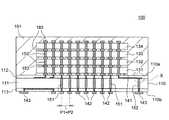
図1は、本発明の好ましい第1の実施形態による半導体記憶装置100の構成を示す略断面図である。 FIG. 1 is a schematic cross-sectional view showing a configuration of a
図1に示すように、本実施形態による半導体記憶装置100は、インターポーザチップ110と、インターポーザチップ110のコア搭載面110a(第1の面)側に搭載された複数(本例では4個)のコアチップ131〜134とを備えており、インターポーザチップ110のコア搭載面110a側に搭載されたコアチップ131〜134は、封止樹脂191によってモールドされている。 As shown in FIG. 1, the
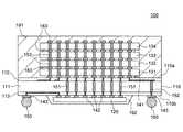
インターポーザチップ110のコア搭載面110aには、第1の内部電極141が形成されており、インターポーザチップ110の実装面110b(第2の面)には、第2の内部電極142及び第3の内部電極143が形成されている。インターポーザチップ110を実装面110b側から見た略平面図である図2に示すように、第2の内部電極142はインターポーザチップ110の中央部に配置されており、第3の内部電極143は第2の内部電極142を取り囲むように、インターポーザチップ110の周縁部に配置されている。第2の内部電極142の電極ピッチP2は、第3の内部電極143の電極ピッチP3よりも狭く、本実施形態では、図1に示すように、第1の内部電極141の電極ピッチP1とほぼ一致している。 A first
また、インターポーザチップ110は、シリコン(Si)からなる半導体基板111と、半導体基板111の両表面に形成された再配線層112,113によって構成されている。半導体基板111には、第1の内部電極141と第2の内部電極142とを接続する第1の貫通電極151と、第1の内部電極141と第3の内部電極143とを接続する第2の貫通電極152が設けられている。本実施形態では、再配線層112によって、平面的な位置が異なる第2の貫通電極152の端部と第1の内部電極141との接続が行われている。また、第2の内部電極142と第3の内部電極143との接続は、再配線層113によって行われている。第1の貫通電極151及び第2の貫通電極152の材料としては、銅(Cu)を用いることが好ましい。第1の貫通電極151及び第2の貫通電極152の材料として銅(Cu)を用いれば、これら貫通電極の配線抵抗を十分に低くすることが可能となる。 The
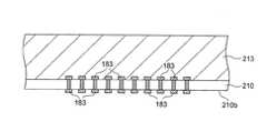
第1の内部電極141はベアチップ状態のコアチップ131の内部端子183に接続される電極である。このため、第1の内部電極141の電極ピッチはP1は非常に狭く、例えば50μm程度に設定される。同様に、第2の内部電極142も、後述するベアチップ状態のインターフェースチップの内部端子に接続される電極であることから、その電極ピッチはP2についても同様に50μm程度に設定される。 The first
本実施形態においては、第1の貫通電極151の電極ピッチが、第1の内部電極141の電極ピッチP1及び第2の内部電極142の電極ピッチP2とほぼ一致しており、これにより、第1の貫通電極151、第1の内部電極141及び第2の内部電極142の平面的な位置は実質的に一致している。したがって、第1の貫通電極151と第1の内部電極141との接続のために、再配線層112を用いた配線の引き回しを行う必要はなく、同様に、第1の貫通電極151と第2の内部電極142との接続のために、再配線層113を用いた配線の引き回しを行う必要はない。 In the present embodiment, the electrode pitch of the first through
このように、本実施形態では、第1の貫通電極151、第1の内部電極141及び第2の内部電極142の平面的な位置が実質的に一致していることから、第1の内部電極141の電極ピッチP1及び第2の内部電極142の電極ピッチP2がいずれも50μmであるとすると、第1の貫通電極151の電極ピッチについても50μm程度となる。このような狭ピッチの貫通電極は、インターポーザチップ110が半導体基板111を母体としているために実現可能であり、樹脂やセラミックなどを用いた通常の基板では、このような狭ピッチの貫通電極を形成することは現実的でない。したがって、インターポーザチップ110の母体として半導体基板111を使用している点は本発明の重要な特徴であり、樹脂やセラミックなどを基板材料として用いた一般的なモジュールとの大きな相違点である。 As described above, in the present embodiment, since the planar positions of the first through
一例として、樹脂やセラミックなどを用いた通常の基板では、貫通電極のピッチを0.2mm以下とすることは困難であり、このため、インターフェースチップ120のサイズが4mm角であるとした場合、第1の貫通電極151の数としては400個が限界となる。これに対し、本発明のように半導体基板111を用いた場合、貫通電極のピッチを0.05mm以下に設定することができ、したがって、400個/mm2以上の密度で貫通電極を形成することが可能となる。As an example, in a normal substrate using resin, ceramic, or the like, it is difficult to set the pitch of the through electrodes to 0.2 mm or less. For this reason, when the size of the
もちろん、再配線によって第1の貫通電極151の電極ピッチを十分に広げれば、樹脂やセラミックなどを用いた通常の基板を使用することが可能であるが、コアチップ131〜134とインターフェースチップ120との間でやり取りされる内部信号の振幅は非常に小さく、また、内部信号は非常に弱い駆動能力で出力される点を考慮すれば、コアチップ131〜134とインターフェースチップ120との間でやり取りされる信号を再配線によって引き回すのではなく、本発明のように極めて短距離で接続することが重要である。 Of course, if the electrode pitch of the first through
図3は、図1に示すX部を拡大して示す拡大断面図である。 FIG. 3 is an enlarged cross-sectional view showing an X portion shown in FIG.
図3に示すように、半導体基板111に設けられた貫通電極152(貫通電極151も同様)の端部は、チタンスパッタ層161と銅スパッタ層162の積層体からなる再配線に接続されており、この再配線は、絶縁層170によって覆われている。チタンスパッタ層161は、銅スパッタ層162と半導体基板111との密着性を高める役割を果たす。特に限定されるものではないが、インターポーザチップ110を構成する半導体基板111は、研磨等によりその厚さが薄型化されていることが好ましい。具体的な厚さとしては、例えば100μm程度に設定すればよい。これにより、必要な機械的強度を確保しつつ、半導体記憶装置100全体の厚さを薄くすることが可能となる。 As shown in FIG. 3, the end of the through electrode 152 (also the through electrode 151) provided on the
一方、コアチップ131〜134は、DRAMのメモリセルが多数形成されたチップであり、メモリセルの他、メモリセルのデータを保持するための回路、つまり、プリチャージ回路やセンスアンプ、アドレスデコーダなどの回路や、コアチップのウエハー試験において良品判定に必要な回路などが形成されたチップである。通常のDRAMとは異なり、外部回路に対する入出力回路などコアに対する周辺回路の一部は備えておらず、このため、コアチップ131〜134単独では使用することはできない。このように、コアチップ131〜134は、外部回路に直接接続されないことから、外部回路に対して信号を出力するのに必要な駆動能力を有するバッファなどは備えられておらず、あくまで半導体記憶装置100内における信号の授受に必要十分な能力を持った入力段及び出力段を備えているに過ぎない。 On the other hand, the core chips 131 to 134 are chips on which a large number of DRAM memory cells are formed. In addition to the memory cells, the core chips 131 to 134 are circuits for holding data of the memory cells, that is, precharge circuits, sense amplifiers, address decoders, and the like. This is a chip on which a circuit and a circuit necessary for non-defective product determination in a core chip wafer test are formed. Unlike a normal DRAM, a part of peripheral circuits for a core such as an input / output circuit for an external circuit is not provided, and therefore the core chips 131 to 134 cannot be used alone. As described above, since the core chips 131 to 134 are not directly connected to the external circuit, the core chips 131 to 134 are not provided with a buffer having a driving capability necessary for outputting a signal to the external circuit. It has only an input stage and an output stage having a necessary and sufficient capability for transmitting and receiving signals.
コアチップ131〜134には、それぞれ第3の貫通電極153及びその両端に設けられた内部端子183が備えられており、これらコアチップ131〜134は、第1の貫通電極151及び第3の貫通電極153を介して、第2の内部電極142とそれぞれ接続されている。本実施形態においては、第1の貫通電極151の電極ピッチと第3の貫通電極153の電極ピッチが実質的に等しく、このため、第1の貫通電極151、第3の貫通電極153、第1の内部電極141及び第2の内部電極142の平面的な位置は実質的に一致している。 Each of the core chips 131 to 134 includes a third through
特に限定されるものではないが、コアチップ131〜134は、研磨等によりその厚さが薄型化されていることが好ましい。具体的な厚さとしては、例えば50μm程度に設定すればよい。 Although not particularly limited, the core chips 131 to 134 are preferably thinned by polishing or the like. A specific thickness may be set to about 50 μm, for example.
このような構成を有する半導体記憶装置100は、いわゆる半製品であり、そのままでは動作しない。実際に完成品とするためには、図4に示すように、インターポーザチップ110の実装面110bに、第2の内部電極142に接続されるようインターフェースチップ120を搭載し、第3の内部電極143上にそれぞれ外部端子150を形成すればよい。インターフェースチップ120は、封止樹脂192によってポッティングモールドされ、これにより物理的に保護される。この状態で、図示しないプリント基板又はモジュール基板に実装することにより、外部回路からは、一つの大きなメモリとして認識されることになる。 The
インターフェースチップ120は、アドレスバッファ、リフレッシュカウンタ、外部回路に対する入出力回路など、コアチップ131〜134に対する周辺回路が形成されたチップであり、第1の内部電極141を介して授受される内部信号の信号幅と、外部端子150を介して授受される信号の信号幅との変換を行う。 The
インターフェースチップ120が搭載されると、外部端子150を介して供給される信号(アドレス、コマンド、ライトデータなど)は、一旦インターフェースチップ120に供給され、インターフェースチップ120によって信号幅が拡大された後、コアチップ131〜134へと供給される。逆に、コアチップ131〜134より供給される信号(リードデータなど)は、一旦インターフェースチップ120に供給され、インターフェースチップ120によって信号幅を縮小された後、外部端子150を介して出力される。 When the
ここで、インターフェースチップ120とコアチップ131〜134とを接続する第1の貫通電極151は、内部信号の伝送を行うために用いられ、外部端子150とコアチップ131〜134とを接続する第2の貫通電極152は、電源供給を行うために用いられる。これは、上述の通り、外部回路に対して信号を出力するのに必要な駆動能力を有するバッファなどがコアチップ131〜134には備えられていないことから、コアチップ131〜134と外部回路との間の信号伝送に関しては、必ずインターフェースチップ120を経由する必要がある一方で、電源供給に関してはこのような制約はなく、外部回路からコアチップ131〜134に対して直接電源供給を行うことができるからである。尚、外部端子150とインターフェースチップ120との接続は、信号伝送及び電源供給とも、再配線層113によって行われる。 Here, the first through
このように、本実施形態による半導体記憶装置100は、コアチップ131〜134をモールドした後に、インターフェースチップ120を後付け可能に構成されていることから、異なる仕様の製品を簡単に作り分けることが可能となる。すなわち、図1に示す状態の半導体記憶装置100を多数ストックしておき、顧客の要望に応じて、適切なインターフェースチップ120を後から搭載すればよいことから、ベアチップ状態のコアチップ131〜134を多量にストックしておく必要がなく、このため、製品の信頼性低下を抑制しつつ、顧客のニーズに応じた機動的な生産を行うことが可能となる。 As described above, since the
次に、本実施形態による半導体記憶装置100の製造方法について説明する。 Next, the method for manufacturing the
まず、図5に示すように、半導体ウェハ200を用意する。半導体ウェハ200には、複数のインターポーザ領域201が含まれている。これら各インターポーザ領域201はそれぞれ1つのインターポーザチップ110となる領域である。このような半導体ウェハ200の各インターポーザ領域201に対し、図6に示すように、一方の表面200b側から複数のトレンチを形成し、これらトレンチを導電部材202によって埋め込む。導電部材202は、最終的に第1の貫通電極151及び第2の貫通電極152となる部材である。 First, as shown in FIG. 5, a
次に、図7に示すように、半導体ウェハ200の一方の表面200bに再配線層113を形成し、さらに、再配線層113上に第2の内部電極142及び第3の内部電極143を形成する。これにより、半導体ウェハ200の一方の表面200b側の加工が完了する。 Next, as shown in FIG. 7, the
次に、図8に示すように、半導体ウェハ200の表面200bにガラスなどの支持基板203を貼り付け、この状態で半導体ウェハ200の他方の表面200aを、トレンチ内に埋め込まれた導電部材202が露出するA−A線まで研磨する。これにより、埋め込まれた導電部材202は第1の貫通電極151及び第2の貫通電極152となる。そして、図9に示すように、研磨により薄型化された半導体ウェハ200の表面200aに再配線層112を形成し、さらに、再配線層112上に第1の内部電極141を形成する。 Next, as shown in FIG. 8, a
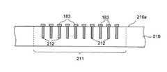
以上により、複数のインターポーザチップ110を含む半導体ウェハ200の加工が完了する。 Thus, the processing of the
一方、図10に示すように、複数のDRAMコア領域211が形成された別の半導体ウェハ210を用意する。この半導体ウェハ210に含まれる各DRAMコア領域211は、それぞれ1つのコアチップ131〜134となる領域である。このような半導体ウェハ210の各DRAMコア領域211に対し、図10に示すように、一方の表面210a側から必要なトレンチを形成し、これを導電部材212によって埋め込む。これら導電部材212は、最終的に第3の貫通電極153となる部材である。尚、トレンチ及びこれを埋め込む導電部材212の形成は、拡散工程によって実際にDRAMコアを作製する前に行っても構わないし、DRAMコアを作製した後に行っても構わない。そして、導電部材212によって埋め込まれたトレンチの上部に、内部端子183を形成する。 On the other hand, as shown in FIG. 10, another
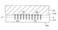
次に、図11に示すように、半導体ウェハ210の表面210aにガラスなどの支持基板213を貼り付け、この状態で半導体ウェハ210の他方の表面210bを、トレンチに埋め込まれた導電部材212が露出するB−B線まで研磨する。これにより、埋め込まれた導電部材212は第3の貫通電極153となる。そして、図12に示すように、露出した第3の貫通電極153の端部に内部端子183を形成し、ダイサーを用いて半導体ウェハ210を個々のDRAMコア領域211に切断すれば、複数のコアチップ131〜134を取り出すことができる。 Next, as shown in FIG. 11, a supporting
以上により、コアチップ131〜134の作製が完了する。 Thus, the fabrication of the core chips 131 to 134 is completed.
このようにして複数のインターポーザチップ110を含む半導体ウェハ200の加工と、コアチップ131〜134の作製が完了すると、図13に示すように、半導体ウェハ200に設けられた第1の内部電極141とコアチップ131に設けられた内部端子183とが正しく接触するようこれらを重ね合わせて熱圧着し、さらに、対応する内部端子183同士が互いに正しく接触するよう、コアチップ132〜134を積層して熱圧着する。このような積層を、半導体ウェハ200に含まれる各インターポーザ領域201に対して行う。 When the processing of the
コアチップ131〜134の積層が完了すると、次に、図14に示すように支持基板203を取り外し、代わりに保護シート204を半導体ウェハ200の表面200bに貼り付ける。この状態で、半導体ウェハ200を封止樹脂191によって一括モールドし、これにより、コアチップ131〜134を半導体ウェハ200上に固定するとともに、物理的に保護する。この場合、図示しないが、封止樹脂191によるモールドを行う前に、アンダーフィルによって半導体ウェハ200及びコアチップ131〜134間に生じている隙間をほぼ完全に埋めておくことが好ましい。図15は、封止樹脂191によって一括モールドした状態における半導体ウェハ200の略平面図である。尚、保護シート204は、モールド時における第2の内部電極142などの汚染を防止するためのシートである。支持基板203によってこのような保護が達成できる場合は、支持基板203をそのまま保護シートの代わりに用いても構わない。When the stacking of the core chips 131 to 134 is completed, the
そして、ダイサーを用いて半導体ウェハ200を個々のインターポーザ領域201に切断すれば、図1に示した半導体記憶装置100を複数取り出すことが可能となる。 If a
その後は、顧客の要望に応じて適切なインターフェースチップ120を搭載し、さらに外部端子150を形成すれば、図4に示した半導体記憶装置100を得ることが可能となる。この場合、半導体記憶装置100を作製した後、直ちにインターフェースチップ120を搭載するのではなく、インターフェースチップ120を搭載していない状態の半導体記憶装置100をいくつかストックしておき、仕様が決定した時点でインターフェースチップ120の搭載及び外部端子150の形成を行えばよい。半導体記憶装置100のストックは、半導体ウェハ200の状態、すなわち未切断の状態であっても構わないし(図15参照)、切断後の状態であっても構わない(図1参照)。いずれの場合も、半導体ウェハ200の表面200bに保護シート204を貼り付けたままの状態でストックしておき、インターフェースチップ120の搭載及び外部端子150の形成の直前に、保護シート204を剥離することが好ましい。これによれば、ストック中における第2の内部電極142などの汚染や腐食を防止することが可能となる。 Thereafter, if an
このように、本実施形態によれば、複数のインターポーザ領域201を有する半導体ウェハ200上にコアチップ131〜134を搭載し、これらコアチップ131〜134を封止樹脂191によって一括モールドしていることから、半製品である半導体記憶装置100を多数個取りすることが可能となる。そして、顧客の要望に応じて、適切なインターフェースチップ120を後から搭載することにより、完成品である半導体記憶装置100を簡単に作製することができる。これにより、顧客のニーズに応じた機動的な生産を行うことが可能となる。 As described above, according to the present embodiment, the core chips 131 to 134 are mounted on the
図16は、本発明の好ましい第2の実施形態による半導体記憶装置300の構成を示す略断面図である。 FIG. 16 is a schematic cross-sectional view showing a configuration of a
本実施形態による半導体記憶装置300は、インターポーザチップ110から再配線層112が削除され、再配線を全て再配線層113にて行っている点において、上記実施形態による半導体記憶装置100と相違している。かかる相違により、第1の内部電極141と第3の内部電極143との平面的な位置合わせについても、再配線層113を用いて行われている。このため、本実施形態では、第1の貫通電極151の電極ピッチ及び第2の貫通電極152の電極ピッチは、いずれも、第1の内部電極141の電極ピッチと実質的に等しくなる。尚、図16では図示されていないが、第2の内部電極142と第3の内部電極143については、上記実施形態と同様、再配線層113を介して接続されている。 The
このように、本実施形態によれば、全ての再配線を再配線層113にて行っていることから、インターポーザチップ110の作製をより容易に行うことが可能となる。 As described above, according to the present embodiment, since all the rewiring is performed in the
図17は、本発明の好ましい第3の実施形態による半導体記憶装置400の構成を示す略断面図である。 FIG. 17 is a schematic cross-sectional view showing a configuration of a
本実施形態による半導体記憶装置400は、第1の貫通電極151と第2の内部電極142とを同一平面位置にて接続するのではなく、再配線層113を用いた引き回しにより、第2の内部電極142の位置調整を行っている点において、上記第2の実施形態による半導体記憶装置300と相違している。本実施形態によれば、第1の内部電極141と第2の内部電極142とで、電極の形成位置を一致させる必要がなくなることから、第2の内部電極142に接続するインターフェースチップ120として、電極位置などが専用に設計されたASICではなく、通常の汎用ASICなどを使用することが可能となる。また、第2の内部電極142の位置調整だけでなく、電極ピッチの変換についても、再配線層113を用いることにより行うことが可能である。 In the
このように、本実施形態によれば、利用可能なインターフェースチップ120の種類が拡大することから、半導体記憶装置の製品コストをより低減することが可能となる。 As described above, according to the present embodiment, since the types of
以上、本発明の好ましい実施形態について説明したが、本発明は、上記の実施形態に限定されることなく、本発明の主旨を逸脱しない範囲で種々の変更が可能であり、それらも本発明の範囲内に包含されるものであることはいうまでもない。 The preferred embodiments of the present invention have been described above, but the present invention is not limited to the above-described embodiments, and various modifications can be made without departing from the spirit of the present invention. Needless to say, it is included in the range.
例えば、上記各実施形態においてはコアチップの数を4個としているが、使用するコアチップの数については特に限定されるものではない。 For example, in each of the above embodiments, the number of core chips is four, but the number of core chips to be used is not particularly limited.
100,300,400 半導体記憶装置
110 インターポーザチップ
110a コア搭載面(第1の面)
110b 実装面(第2の面)
111 半導体基板
112,113 再配線層
120 インターフェースチップ
131〜134 コアチップ
141 第1の内部電極
142 第2の内部電極
143 第3の内部電極
150 外部端子
151 第1の貫通電極
152 第2の貫通電極
153 第3の貫通電極
161 チタンスパッタ層
162 銅スパッタ層
170 絶縁層
183 内部端子
191,192 封止樹脂
200,210 半導体ウェハ
200a,200b 半導体ウェハの表面
201 インターポーザ領域
202,212 導電部材
203,213 支持基板
204 保護シート
210a,210b 半導体ウェハの表面
211 コア領域100, 300, 400
110b Mounting surface (second surface)
Claims (12)
Translated fromJapanese前記インターポーザチップの前記第1の面側に搭載され、前記第1の内部電極に接続された複数のコアチップとを備え、
前記複数の第2の内部電極は、前記第1の内部電極及び前記第1の貫通電極と平面的に重なる位置で直線的に接続された電極と、前記再配線層の引き回しにより、平面的に重なる位置で接続された前記第1の内部電極及び前記第1の貫通電極と平面的に異なる位置で接続された電極とを含むことを特徴とする半導体記憶装置。A semiconductor substrate,a plurality of first internal electrodesformed on a first surface of thesemiconductor substrate,a rewiring layer formed on a second surface opposite to the first surface of thesemiconductor substrate, the second the centrally disposed region of the surface, said plurality of second internal electrodesformed on the redistributionlayer, the plurality of thirdformed on a second ofthe re-wiring layer so as to surround the internal electrode internal electrodesformed on the semiconductor substrate, the first plurality of first connecting the portion of a part and the second internal electrodes of the internal electrodethrough the redistribution layer of the throughelectrode, and the formed on a semiconductor substrate, said first interposercomprising a plurality of second through electrode for connecting the portion of the other of said part third internal electrodethrough the redistribution layer of the internal electrode tip and ,
A plurality of core chips mounted on the first surface side of the interposer chip and connected to the first internal electrode;
The plurality of second internal electrodes are planarly formed by extending the redistribution layer and electrodes linearly connected to the first internal electrode and the first through electrode in a position overlapping the plane. A semiconductor memory devicecomprising: the first internal electrode connected at an overlapping position and an electrode connected at a position different in plan from the first through electrode .
Priority Applications (5)
| Application Number | Priority Date | Filing Date | Title |
|---|---|---|---|
| JP2005191257AJP4507101B2 (en) | 2005-06-30 | 2005-06-30 | Semiconductor memory device and manufacturing method thereof |
| US11/476,145US7576433B2 (en) | 2005-06-30 | 2006-06-28 | Semiconductor memory device and manufacturing method thereof |
| US12/537,723US7893540B2 (en) | 2005-06-30 | 2009-08-07 | Semiconductor memory device and manufacturing method thereof |
| US13/005,350US8298940B2 (en) | 2005-06-30 | 2011-01-12 | Semiconductor memory device and manufacturing method thereof |
| US13/621,134US8513121B2 (en) | 2005-06-30 | 2012-09-15 | Semiconductor memory device and manufacturing method thereof |
Applications Claiming Priority (1)
| Application Number | Priority Date | Filing Date | Title |
|---|---|---|---|
| JP2005191257AJP4507101B2 (en) | 2005-06-30 | 2005-06-30 | Semiconductor memory device and manufacturing method thereof |
Publications (3)
| Publication Number | Publication Date |
|---|---|
| JP2007012848A JP2007012848A (en) | 2007-01-18 |
| JP2007012848A5 JP2007012848A5 (en) | 2007-04-19 |
| JP4507101B2true JP4507101B2 (en) | 2010-07-21 |
Family
ID=37588457
Family Applications (1)
| Application Number | Title | Priority Date | Filing Date |
|---|---|---|---|
| JP2005191257AExpired - Fee RelatedJP4507101B2 (en) | 2005-06-30 | 2005-06-30 | Semiconductor memory device and manufacturing method thereof |
Country Status (2)
| Country | Link |
|---|---|
| US (4) | US7576433B2 (en) |
| JP (1) | JP4507101B2 (en) |
Cited By (1)
| Publication number | Priority date | Publication date | Assignee | Title |
|---|---|---|---|---|
| US10083939B2 (en) | 2016-05-17 | 2018-09-25 | Samsung Electronics Co., Ltd. | Semiconductor package |
Families Citing this family (204)
| Publication number | Priority date | Publication date | Assignee | Title |
|---|---|---|---|---|
| JP4340517B2 (en) | 2003-10-30 | 2009-10-07 | Okiセミコンダクタ株式会社 | Semiconductor device and manufacturing method thereof |
| JP4577688B2 (en) | 2005-05-09 | 2010-11-10 | エルピーダメモリ株式会社 | Semiconductor chip selection method, semiconductor chip, and semiconductor integrated circuit device |
| US7486525B2 (en)* | 2006-08-04 | 2009-02-03 | International Business Machines Corporation | Temporary chip attach carrier |
| KR100777926B1 (en)* | 2006-08-29 | 2007-11-21 | 동부일렉트로닉스 주식회사 | Semiconductor device and manufacturing method |
| US8110899B2 (en)* | 2006-12-20 | 2012-02-07 | Intel Corporation | Method for incorporating existing silicon die into 3D integrated stack |
| KR100875955B1 (en)* | 2007-01-25 | 2008-12-26 | 삼성전자주식회사 | Stacked package and its manufacturing method |
| JP5125185B2 (en)* | 2007-04-03 | 2013-01-23 | 株式会社ニコン | Semiconductor device |
| KR100906065B1 (en)* | 2007-07-12 | 2009-07-03 | 주식회사 동부하이텍 | Semiconductor chip, manufacturing method thereof and laminated package having same |
| JP5570689B2 (en)* | 2007-07-23 | 2014-08-13 | ピーエスフォー ルクスコ エスエイアールエル | Stacked memory |
| JP2009049087A (en)* | 2007-08-16 | 2009-03-05 | Panasonic Corp | Electronic component and method for manufacturing electronic component |
| US7623365B2 (en) | 2007-08-29 | 2009-11-24 | Micron Technology, Inc. | Memory device interface methods, apparatus, and systems |
| US7898091B2 (en)* | 2007-10-02 | 2011-03-01 | Sandisk Corporation | Multi-host interface controller with USB PHY/analog functions integrated in a single package |
| US7715227B2 (en)* | 2007-10-02 | 2010-05-11 | Freescale Semiconductor, Inc. | Programmable ROM using two bonded strata |
| US20090115026A1 (en)* | 2007-11-05 | 2009-05-07 | Texas Instruments Incorporated | Semiconductor device having through-silicon vias for high current,high frequency, and heat dissipation |
| JP5306634B2 (en)* | 2007-11-22 | 2013-10-02 | 新光電気工業株式会社 | WIRING BOARD, SEMICONDUCTOR DEVICE, AND WIRING BOARD MANUFACTURING METHOD |
| JP2009139273A (en)* | 2007-12-07 | 2009-06-25 | Elpida Memory Inc | Laminated semiconductor device, and continuity test |
| JP5372382B2 (en)* | 2008-01-09 | 2013-12-18 | ピーエスフォー ルクスコ エスエイアールエル | Semiconductor device |
| KR100900236B1 (en) | 2008-01-25 | 2009-05-29 | 주식회사 하이닉스반도체 | Semiconductor chip and laminated semiconductor package having same |
| EP2104138A1 (en) | 2008-03-18 | 2009-09-23 | EV Group E. Thallner GmbH | Method for bonding chips onto a wafer |
| US7872332B2 (en)* | 2008-09-11 | 2011-01-18 | Micron Technology, Inc. | Interconnect structures for stacked dies, including penetrating structures for through-silicon vias, and associated systems and methods |
| US8106520B2 (en) | 2008-09-11 | 2012-01-31 | Micron Technology, Inc. | Signal delivery in stacked device |
| JP2010080752A (en)* | 2008-09-26 | 2010-04-08 | Panasonic Corp | Method of manufacturing semiconductor device |
| KR20100048610A (en)* | 2008-10-31 | 2010-05-11 | 삼성전자주식회사 | Semiconductor fackage and forming method of the same |
| JP5471268B2 (en) | 2008-12-26 | 2014-04-16 | 大日本印刷株式会社 | Through electrode substrate and manufacturing method thereof |
| JP4900508B2 (en)* | 2008-12-26 | 2012-03-21 | 大日本印刷株式会社 | Through electrode substrate and manufacturing method thereof |
| US7894230B2 (en)* | 2009-02-24 | 2011-02-22 | Mosaid Technologies Incorporated | Stacked semiconductor devices including a master device |
| JP5340789B2 (en)* | 2009-04-06 | 2013-11-13 | 新光電気工業株式会社 | Electronic device and manufacturing method thereof |
| JP2010245383A (en)* | 2009-04-08 | 2010-10-28 | Elpida Memory Inc | Semiconductor device and method of manufacturing the same |
| US8039304B2 (en)* | 2009-08-12 | 2011-10-18 | Stats Chippac, Ltd. | Semiconductor device and method of dual-molding die formed on opposite sides of build-up interconnect structures |
| EP2299486B1 (en)* | 2009-09-18 | 2015-02-18 | EV Group E. Thallner GmbH | Method for bonding chips to wafers |
| US10910364B2 (en) | 2009-10-12 | 2021-02-02 | Monolitaic 3D Inc. | 3D semiconductor device |
| US11984445B2 (en) | 2009-10-12 | 2024-05-14 | Monolithic 3D Inc. | 3D semiconductor devices and structures with metal layers |
| US11374118B2 (en) | 2009-10-12 | 2022-06-28 | Monolithic 3D Inc. | Method to form a 3D integrated circuit |
| US12027518B1 (en) | 2009-10-12 | 2024-07-02 | Monolithic 3D Inc. | 3D semiconductor devices and structures with metal layers |
| US11018133B2 (en) | 2009-10-12 | 2021-05-25 | Monolithic 3D Inc. | 3D integrated circuit |
| US8218380B2 (en) | 2009-10-30 | 2012-07-10 | Apple Inc. | Degradation equalization for a memory |
| KR101123804B1 (en)* | 2009-11-20 | 2012-03-12 | 주식회사 하이닉스반도체 | Semiconductor chip and stacked semiconductor package havng the same |
| JP5581064B2 (en)* | 2010-01-14 | 2014-08-27 | パナソニック株式会社 | Semiconductor device |
| US10672748B1 (en)* | 2010-06-02 | 2020-06-02 | Maxim Integrated Products, Inc. | Use of device assembly for a generalization of three-dimensional heterogeneous technologies integration |
| TWI493633B (en)* | 2010-08-13 | 2015-07-21 | Ineffable Cellular Ltd Liability Company | Stacking method and stacking carrier |
| KR101251916B1 (en)* | 2010-08-27 | 2013-04-08 | 에스케이하이닉스 주식회사 | Semiconductor integrated circuit |
| KR101728067B1 (en) | 2010-09-03 | 2017-04-18 | 삼성전자 주식회사 | Semiconductor memory device |
| US12362219B2 (en) | 2010-11-18 | 2025-07-15 | Monolithic 3D Inc. | 3D semiconductor memory device and structure |
| US11482440B2 (en) | 2010-12-16 | 2022-10-25 | Monolithic 3D Inc. | 3D semiconductor device and structure with a built-in test circuit for repairing faulty circuits |
| US11469271B2 (en) | 2010-10-11 | 2022-10-11 | Monolithic 3D Inc. | Method to produce 3D semiconductor devices and structures with memory |
| US11158674B2 (en) | 2010-10-11 | 2021-10-26 | Monolithic 3D Inc. | Method to produce a 3D semiconductor device and structure |
| US11600667B1 (en) | 2010-10-11 | 2023-03-07 | Monolithic 3D Inc. | Method to produce 3D semiconductor devices and structures with memory |
| US11024673B1 (en) | 2010-10-11 | 2021-06-01 | Monolithic 3D Inc. | 3D semiconductor device and structure |
| US11315980B1 (en) | 2010-10-11 | 2022-04-26 | Monolithic 3D Inc. | 3D semiconductor device and structure with transistors |
| US11018191B1 (en) | 2010-10-11 | 2021-05-25 | Monolithic 3D Inc. | 3D semiconductor device and structure |
| US11227897B2 (en) | 2010-10-11 | 2022-01-18 | Monolithic 3D Inc. | Method for producing a 3D semiconductor memory device and structure |
| US10896931B1 (en) | 2010-10-11 | 2021-01-19 | Monolithic 3D Inc. | 3D semiconductor device and structure |
| US11257867B1 (en) | 2010-10-11 | 2022-02-22 | Monolithic 3D Inc. | 3D semiconductor device and structure with oxide bonds |
| US11133344B2 (en) | 2010-10-13 | 2021-09-28 | Monolithic 3D Inc. | Multilevel semiconductor device and structure with image sensors |
| US11984438B2 (en) | 2010-10-13 | 2024-05-14 | Monolithic 3D Inc. | Multilevel semiconductor device and structure with oxide bonding |
| US12080743B2 (en) | 2010-10-13 | 2024-09-03 | Monolithic 3D Inc. | Multilevel semiconductor device and structure with image sensors and wafer bonding |
| US11855114B2 (en) | 2010-10-13 | 2023-12-26 | Monolithic 3D Inc. | Multilevel semiconductor device and structure with image sensors and wafer bonding |
| US11694922B2 (en) | 2010-10-13 | 2023-07-04 | Monolithic 3D Inc. | Multilevel semiconductor device and structure with oxide bonding |
| US11869915B2 (en) | 2010-10-13 | 2024-01-09 | Monolithic 3D Inc. | Multilevel semiconductor device and structure with image sensors and wafer bonding |
| US12360310B2 (en) | 2010-10-13 | 2025-07-15 | Monolithic 3D Inc. | Multilevel semiconductor device and structure with oxide bonding |
| US10943934B2 (en) | 2010-10-13 | 2021-03-09 | Monolithic 3D Inc. | Multilevel semiconductor device and structure |
| US10978501B1 (en) | 2010-10-13 | 2021-04-13 | Monolithic 3D Inc. | Multilevel semiconductor device and structure with waveguides |
| US10998374B1 (en) | 2010-10-13 | 2021-05-04 | Monolithic 3D Inc. | Multilevel semiconductor device and structure |
| US12094892B2 (en) | 2010-10-13 | 2024-09-17 | Monolithic 3D Inc. | 3D micro display device and structure |
| US11404466B2 (en) | 2010-10-13 | 2022-08-02 | Monolithic 3D Inc. | Multilevel semiconductor device and structure with image sensors |
| US11929372B2 (en) | 2010-10-13 | 2024-03-12 | Monolithic 3D Inc. | Multilevel semiconductor device and structure with image sensors and wafer bonding |
| US11043523B1 (en) | 2010-10-13 | 2021-06-22 | Monolithic 3D Inc. | Multilevel semiconductor device and structure with image sensors |
| US11164898B2 (en) | 2010-10-13 | 2021-11-02 | Monolithic 3D Inc. | Multilevel semiconductor device and structure |
| US11163112B2 (en) | 2010-10-13 | 2021-11-02 | Monolithic 3D Inc. | Multilevel semiconductor device and structure with electromagnetic modulators |
| US11063071B1 (en) | 2010-10-13 | 2021-07-13 | Monolithic 3D Inc. | Multilevel semiconductor device and structure with waveguides |
| US10833108B2 (en) | 2010-10-13 | 2020-11-10 | Monolithic 3D Inc. | 3D microdisplay device and structure |
| US11605663B2 (en) | 2010-10-13 | 2023-03-14 | Monolithic 3D Inc. | Multilevel semiconductor device and structure with image sensors and wafer bonding |
| US11855100B2 (en) | 2010-10-13 | 2023-12-26 | Monolithic 3D Inc. | Multilevel semiconductor device and structure with oxide bonding |
| US11327227B2 (en) | 2010-10-13 | 2022-05-10 | Monolithic 3D Inc. | Multilevel semiconductor device and structure with electromagnetic modulators |
| US11437368B2 (en) | 2010-10-13 | 2022-09-06 | Monolithic 3D Inc. | Multilevel semiconductor device and structure with oxide bonding |
| KR101690487B1 (en)* | 2010-11-08 | 2016-12-28 | 삼성전자주식회사 | Semiconductor device and fabrication method thereof |
| US11610802B2 (en) | 2010-11-18 | 2023-03-21 | Monolithic 3D Inc. | Method for producing a 3D semiconductor device and structure with single crystal transistors and metal gate electrodes |
| US11508605B2 (en) | 2010-11-18 | 2022-11-22 | Monolithic 3D Inc. | 3D semiconductor memory device and structure |
| US11784082B2 (en) | 2010-11-18 | 2023-10-10 | Monolithic 3D Inc. | 3D semiconductor device and structure with bonding |
| US11355381B2 (en) | 2010-11-18 | 2022-06-07 | Monolithic 3D Inc. | 3D semiconductor memory device and structure |
| US11569117B2 (en) | 2010-11-18 | 2023-01-31 | Monolithic 3D Inc. | 3D semiconductor device and structure with single-crystal layers |
| US12144190B2 (en) | 2010-11-18 | 2024-11-12 | Monolithic 3D Inc. | 3D semiconductor device and structure with bonding and memory cells preliminary class |
| US11004719B1 (en) | 2010-11-18 | 2021-05-11 | Monolithic 3D Inc. | Methods for producing a 3D semiconductor memory device and structure |
| US11107721B2 (en) | 2010-11-18 | 2021-08-31 | Monolithic 3D Inc. | 3D semiconductor device and structure with NAND logic |
| US11482439B2 (en) | 2010-11-18 | 2022-10-25 | Monolithic 3D Inc. | Methods for producing a 3D semiconductor memory device comprising charge trap junction-less transistors |
| US11031275B2 (en) | 2010-11-18 | 2021-06-08 | Monolithic 3D Inc. | 3D semiconductor device and structure with memory |
| US11901210B2 (en) | 2010-11-18 | 2024-02-13 | Monolithic 3D Inc. | 3D semiconductor device and structure with memory |
| US11355380B2 (en) | 2010-11-18 | 2022-06-07 | Monolithic 3D Inc. | Methods for producing 3D semiconductor memory device and structure utilizing alignment marks |
| US12243765B2 (en) | 2010-11-18 | 2025-03-04 | Monolithic 3D Inc. | 3D semiconductor device and structure with metal layers and memory cells |
| US11615977B2 (en) | 2010-11-18 | 2023-03-28 | Monolithic 3D Inc. | 3D semiconductor memory device and structure |
| US11735462B2 (en) | 2010-11-18 | 2023-08-22 | Monolithic 3D Inc. | 3D semiconductor device and structure with single-crystal layers |
| US12068187B2 (en) | 2010-11-18 | 2024-08-20 | Monolithic 3D Inc. | 3D semiconductor device and structure with bonding and DRAM memory cells |
| US11211279B2 (en) | 2010-11-18 | 2021-12-28 | Monolithic 3D Inc. | Method for processing a 3D integrated circuit and structure |
| US11804396B2 (en) | 2010-11-18 | 2023-10-31 | Monolithic 3D Inc. | Methods for producing a 3D semiconductor device and structure with memory cells and multiple metal layers |
| US11164770B1 (en) | 2010-11-18 | 2021-11-02 | Monolithic 3D Inc. | Method for producing a 3D semiconductor memory device and structure |
| US12154817B1 (en) | 2010-11-18 | 2024-11-26 | Monolithic 3D Inc. | Methods for producing a 3D semiconductor memory device and structure |
| US12125737B1 (en) | 2010-11-18 | 2024-10-22 | Monolithic 3D Inc. | 3D semiconductor device and structure with metal layers and memory cells |
| US11923230B1 (en) | 2010-11-18 | 2024-03-05 | Monolithic 3D Inc. | 3D semiconductor device and structure with bonding |
| US12136562B2 (en) | 2010-11-18 | 2024-11-05 | Monolithic 3D Inc. | 3D semiconductor device and structure with single-crystal layers |
| US12033884B2 (en) | 2010-11-18 | 2024-07-09 | Monolithic 3D Inc. | Methods for producing a 3D semiconductor device and structure with memory cells and multiple metal layers |
| US11482438B2 (en) | 2010-11-18 | 2022-10-25 | Monolithic 3D Inc. | Methods for producing a 3D semiconductor memory device and structure |
| US11495484B2 (en) | 2010-11-18 | 2022-11-08 | Monolithic 3D Inc. | 3D semiconductor devices and structures with at least two single-crystal layers |
| US12272586B2 (en) | 2010-11-18 | 2025-04-08 | Monolithic 3D Inc. | 3D semiconductor memory device and structure with memory and metal layers |
| US11443971B2 (en) | 2010-11-18 | 2022-09-13 | Monolithic 3D Inc. | 3D semiconductor device and structure with memory |
| US12100611B2 (en) | 2010-11-18 | 2024-09-24 | Monolithic 3D Inc. | Methods for producing a 3D semiconductor device and structure with memory cells and multiple metal layers |
| US11094576B1 (en) | 2010-11-18 | 2021-08-17 | Monolithic 3D Inc. | Methods for producing a 3D semiconductor memory device and structure |
| US11854857B1 (en) | 2010-11-18 | 2023-12-26 | Monolithic 3D Inc. | Methods for producing a 3D semiconductor device and structure with memory cells and multiple metal layers |
| US11862503B2 (en) | 2010-11-18 | 2024-01-02 | Monolithic 3D Inc. | Method for producing a 3D semiconductor device and structure with memory cells and multiple metal layers |
| US11521888B2 (en) | 2010-11-18 | 2022-12-06 | Monolithic 3D Inc. | 3D semiconductor device and structure with high-k metal gate transistors |
| US11018042B1 (en) | 2010-11-18 | 2021-05-25 | Monolithic 3D Inc. | 3D semiconductor memory device and structure |
| JP2012156238A (en)* | 2011-01-25 | 2012-08-16 | Elpida Memory Inc | Semiconductor device |
| KR101719636B1 (en)* | 2011-01-28 | 2017-04-05 | 삼성전자 주식회사 | Semiconductor device and fabricating method thereof |
| KR101817159B1 (en)* | 2011-02-17 | 2018-02-22 | 삼성전자 주식회사 | Semiconductor package having TSV interposer and method of manufacturing the same |
| US8552567B2 (en) | 2011-07-27 | 2013-10-08 | Micron Technology, Inc. | Semiconductor die assemblies, semiconductor devices including same, and methods of fabrication |
| US8937309B2 (en) | 2011-08-08 | 2015-01-20 | Micron Technology, Inc. | Semiconductor die assemblies, semiconductor devices including same, and methods of fabrication |
| JP5936968B2 (en) | 2011-09-22 | 2016-06-22 | 株式会社東芝 | Semiconductor device and manufacturing method thereof |
| US8628636B2 (en)* | 2012-01-13 | 2014-01-14 | Advance Materials Corporation | Method of manufacturing a package substrate |
| JP5912616B2 (en)* | 2012-02-08 | 2016-04-27 | 株式会社ジェイデバイス | Semiconductor device and manufacturing method thereof |
| TWI469312B (en) | 2012-03-09 | 2015-01-11 | Ind Tech Res Inst | Chip stack structure and method of fabricating the same |
| US11694944B1 (en) | 2012-04-09 | 2023-07-04 | Monolithic 3D Inc. | 3D semiconductor device and structure with metal layers and a connective path |
| US11735501B1 (en) | 2012-04-09 | 2023-08-22 | Monolithic 3D Inc. | 3D semiconductor device and structure with metal layers and a connective path |
| US11616004B1 (en) | 2012-04-09 | 2023-03-28 | Monolithic 3D Inc. | 3D semiconductor device and structure with metal layers and a connective path |
| US11164811B2 (en) | 2012-04-09 | 2021-11-02 | Monolithic 3D Inc. | 3D semiconductor device with isolation layers and oxide-to-oxide bonding |
| US11410912B2 (en) | 2012-04-09 | 2022-08-09 | Monolithic 3D Inc. | 3D semiconductor device with vias and isolation layers |
| US11881443B2 (en) | 2012-04-09 | 2024-01-23 | Monolithic 3D Inc. | 3D semiconductor device and structure with metal layers and a connective path |
| US11476181B1 (en) | 2012-04-09 | 2022-10-18 | Monolithic 3D Inc. | 3D semiconductor device and structure with metal layers |
| US11088050B2 (en) | 2012-04-09 | 2021-08-10 | Monolithic 3D Inc. | 3D semiconductor device with isolation layers |
| US11594473B2 (en) | 2012-04-09 | 2023-02-28 | Monolithic 3D Inc. | 3D semiconductor device and structure with metal layers and a connective path |
| JP2014011169A (en) | 2012-06-27 | 2014-01-20 | Ps4 Luxco S A R L | Silicon interposer and semiconductor device with the same |
| JP5968736B2 (en)* | 2012-09-14 | 2016-08-10 | ルネサスエレクトロニクス株式会社 | Semiconductor device |
| US20140145348A1 (en)* | 2012-11-26 | 2014-05-29 | Samsung Electro-Mechanics Co., Ltd. | Rf (radio frequency) module and method of maufacturing the same |
| US11916045B2 (en) | 2012-12-22 | 2024-02-27 | Monolithic 3D Inc. | 3D semiconductor device and structure with metal layers |
| US11784169B2 (en) | 2012-12-22 | 2023-10-10 | Monolithic 3D Inc. | 3D semiconductor device and structure with metal layers |
| US11217565B2 (en) | 2012-12-22 | 2022-01-04 | Monolithic 3D Inc. | Method to form a 3D semiconductor device and structure |
| US11018116B2 (en) | 2012-12-22 | 2021-05-25 | Monolithic 3D Inc. | Method to form a 3D semiconductor device and structure |
| US11063024B1 (en) | 2012-12-22 | 2021-07-13 | Monlithic 3D Inc. | Method to form a 3D semiconductor device and structure |
| US11961827B1 (en) | 2012-12-22 | 2024-04-16 | Monolithic 3D Inc. | 3D semiconductor device and structure with metal layers |
| US12051674B2 (en) | 2012-12-22 | 2024-07-30 | Monolithic 3D Inc. | 3D semiconductor device and structure with metal layers |
| US11309292B2 (en) | 2012-12-22 | 2022-04-19 | Monolithic 3D Inc. | 3D semiconductor device and structure with metal layers |
| US11967583B2 (en) | 2012-12-22 | 2024-04-23 | Monolithic 3D Inc. | 3D semiconductor device and structure with metal layers |
| US11004694B1 (en) | 2012-12-29 | 2021-05-11 | Monolithic 3D Inc. | 3D semiconductor device and structure |
| US11430667B2 (en) | 2012-12-29 | 2022-08-30 | Monolithic 3D Inc. | 3D semiconductor device and structure with bonding |
| US12249538B2 (en) | 2012-12-29 | 2025-03-11 | Monolithic 3D Inc. | 3D semiconductor device and structure including power distribution grids |
| US11430668B2 (en) | 2012-12-29 | 2022-08-30 | Monolithic 3D Inc. | 3D semiconductor device and structure with bonding |
| US11087995B1 (en) | 2012-12-29 | 2021-08-10 | Monolithic 3D Inc. | 3D semiconductor device and structure |
| US10903089B1 (en) | 2012-12-29 | 2021-01-26 | Monolithic 3D Inc. | 3D semiconductor device and structure |
| US11177140B2 (en) | 2012-12-29 | 2021-11-16 | Monolithic 3D Inc. | 3D semiconductor device and structure |
| US11869965B2 (en) | 2013-03-11 | 2024-01-09 | Monolithic 3D Inc. | 3D semiconductor device and structure with metal layers and memory cells |
| US12094965B2 (en) | 2013-03-11 | 2024-09-17 | Monolithic 3D Inc. | 3D semiconductor device and structure with metal layers and memory cells |
| US8902663B1 (en) | 2013-03-11 | 2014-12-02 | Monolithic 3D Inc. | Method of maintaining a memory state |
| US11935949B1 (en) | 2013-03-11 | 2024-03-19 | Monolithic 3D Inc. | 3D semiconductor device and structure with metal layers and memory cells |
| US11088130B2 (en) | 2014-01-28 | 2021-08-10 | Monolithic 3D Inc. | 3D semiconductor device and structure |
| US10840239B2 (en)* | 2014-08-26 | 2020-11-17 | Monolithic 3D Inc. | 3D semiconductor device and structure |
| US11398569B2 (en) | 2013-03-12 | 2022-07-26 | Monolithic 3D Inc. | 3D semiconductor device and structure |
| US12100646B2 (en) | 2013-03-12 | 2024-09-24 | Monolithic 3D Inc. | 3D semiconductor device and structure with metal layers |
| US11923374B2 (en) | 2013-03-12 | 2024-03-05 | Monolithic 3D Inc. | 3D semiconductor device and structure with metal layers |
| US11720736B2 (en) | 2013-04-15 | 2023-08-08 | Monolithic 3D Inc. | Automation methods for 3D integrated circuits and devices |
| US11487928B2 (en) | 2013-04-15 | 2022-11-01 | Monolithic 3D Inc. | Automation for monolithic 3D devices |
| US11574109B1 (en) | 2013-04-15 | 2023-02-07 | Monolithic 3D Inc | Automation methods for 3D integrated circuits and devices |
| US11270055B1 (en) | 2013-04-15 | 2022-03-08 | Monolithic 3D Inc. | Automation for monolithic 3D devices |
| US11341309B1 (en) | 2013-04-15 | 2022-05-24 | Monolithic 3D Inc. | Automation for monolithic 3D devices |
| US9324698B2 (en)* | 2013-08-13 | 2016-04-26 | Taiwan Semiconductor Manufacturing Company, Ltd. | Multi-chip structure and method of forming same |
| CN103545297A (en)* | 2013-10-25 | 2014-01-29 | 矽力杰半导体技术(杭州)有限公司 | Multi-chip overlapping and packing structure and manufacturing method thereof |
| US12094829B2 (en) | 2014-01-28 | 2024-09-17 | Monolithic 3D Inc. | 3D semiconductor device and structure |
| US11107808B1 (en) | 2014-01-28 | 2021-08-31 | Monolithic 3D Inc. | 3D semiconductor device and structure |
| US11031394B1 (en) | 2014-01-28 | 2021-06-08 | Monolithic 3D Inc. | 3D semiconductor device and structure |
| JP2016058627A (en)* | 2014-09-11 | 2016-04-21 | 株式会社東芝 | Semiconductor device |
| US11056468B1 (en) | 2015-04-19 | 2021-07-06 | Monolithic 3D Inc. | 3D semiconductor device and structure |
| US11011507B1 (en) | 2015-04-19 | 2021-05-18 | Monolithic 3D Inc. | 3D semiconductor device and structure |
| US10825779B2 (en) | 2015-04-19 | 2020-11-03 | Monolithic 3D Inc. | 3D semiconductor device and structure |
| US11956952B2 (en) | 2015-08-23 | 2024-04-09 | Monolithic 3D Inc. | Semiconductor memory device and structure |
| US11937422B2 (en) | 2015-11-07 | 2024-03-19 | Monolithic 3D Inc. | Semiconductor memory device and structure |
| US11978731B2 (en) | 2015-09-21 | 2024-05-07 | Monolithic 3D Inc. | Method to produce a multi-level semiconductor memory device and structure |
| US12250830B2 (en) | 2015-09-21 | 2025-03-11 | Monolithic 3D Inc. | 3D semiconductor memory devices and structures |
| US12178055B2 (en) | 2015-09-21 | 2024-12-24 | Monolithic 3D Inc. | 3D semiconductor memory devices and structures |
| US11114427B2 (en) | 2015-11-07 | 2021-09-07 | Monolithic 3D Inc. | 3D semiconductor processor and memory device and structure |
| US12100658B2 (en) | 2015-09-21 | 2024-09-24 | Monolithic 3D Inc. | Method to produce a 3D multilayer semiconductor device and structure |
| US12120880B1 (en) | 2015-10-24 | 2024-10-15 | Monolithic 3D Inc. | 3D semiconductor device and structure with logic and memory |
| US12219769B2 (en) | 2015-10-24 | 2025-02-04 | Monolithic 3D Inc. | 3D semiconductor device and structure with logic and memory |
| US12016181B2 (en) | 2015-10-24 | 2024-06-18 | Monolithic 3D Inc. | 3D semiconductor device and structure with logic and memory |
| US11296115B1 (en) | 2015-10-24 | 2022-04-05 | Monolithic 3D Inc. | 3D semiconductor device and structure |
| US11114464B2 (en) | 2015-10-24 | 2021-09-07 | Monolithic 3D Inc. | 3D semiconductor device and structure |
| US12035531B2 (en) | 2015-10-24 | 2024-07-09 | Monolithic 3D Inc. | 3D semiconductor device and structure with logic and memory |
| US11991884B1 (en) | 2015-10-24 | 2024-05-21 | Monolithic 3D Inc. | 3D semiconductor device and structure with logic and memory |
| US10847540B2 (en) | 2015-10-24 | 2020-11-24 | Monolithic 3D Inc. | 3D semiconductor memory device and structure |
| US11869591B2 (en) | 2016-10-10 | 2024-01-09 | Monolithic 3D Inc. | 3D memory devices and structures with control circuits |
| US11930648B1 (en) | 2016-10-10 | 2024-03-12 | Monolithic 3D Inc. | 3D memory devices and structures with metal layers |
| US11711928B2 (en) | 2016-10-10 | 2023-07-25 | Monolithic 3D Inc. | 3D memory devices and structures with control circuits |
| US11329059B1 (en) | 2016-10-10 | 2022-05-10 | Monolithic 3D Inc. | 3D memory devices and structures with thinned single crystal substrates |
| US11251149B2 (en) | 2016-10-10 | 2022-02-15 | Monolithic 3D Inc. | 3D memory device and structure |
| US12225704B2 (en) | 2016-10-10 | 2025-02-11 | Monolithic 3D Inc. | 3D memory devices and structures with memory arrays and metal layers |
| US11812620B2 (en) | 2016-10-10 | 2023-11-07 | Monolithic 3D Inc. | 3D DRAM memory devices and structures with control circuits |
| JP2018107394A (en)* | 2016-12-28 | 2018-07-05 | 新光電気工業株式会社 | Wiring board, electronic component device and manufacturing method thereof |
| JP2018152147A (en) | 2017-03-10 | 2018-09-27 | 東芝メモリ株式会社 | Semiconductor memory device and method |
| JP6679528B2 (en)* | 2017-03-22 | 2020-04-15 | キオクシア株式会社 | Semiconductor device |
| CN109712966A (en)* | 2017-10-25 | 2019-05-03 | 中芯国际集成电路制造(上海)有限公司 | Chip-packaging structure and forming method thereof |
| KR102551751B1 (en) | 2018-11-06 | 2023-07-05 | 삼성전자주식회사 | Semiconductor packages |
| US11018156B2 (en) | 2019-04-08 | 2021-05-25 | Monolithic 3D Inc. | 3D memory semiconductor devices and structures |
| US11158652B1 (en) | 2019-04-08 | 2021-10-26 | Monolithic 3D Inc. | 3D memory semiconductor devices and structures |
| US10892016B1 (en) | 2019-04-08 | 2021-01-12 | Monolithic 3D Inc. | 3D memory semiconductor devices and structures |
| US11763864B2 (en) | 2019-04-08 | 2023-09-19 | Monolithic 3D Inc. | 3D memory semiconductor devices and structures with bit-line pillars |
| US11296106B2 (en) | 2019-04-08 | 2022-04-05 | Monolithic 3D Inc. | 3D memory semiconductor devices and structures |
| US11587918B2 (en) | 2019-12-17 | 2023-02-21 | Micron Technology, Inc. | Semiconductor devices, semiconductor device packages, electronic systems including same, and related methods |
| KR20230035945A (en)* | 2021-09-06 | 2023-03-14 | 삼성전자주식회사 | semiconductor package |
Family Cites Families (27)
| Publication number | Priority date | Publication date | Assignee | Title |
|---|---|---|---|---|
| US4074342A (en)* | 1974-12-20 | 1978-02-14 | International Business Machines Corporation | Electrical package for lsi devices and assembly process therefor |
| JP3920399B2 (en)* | 1997-04-25 | 2007-05-30 | 株式会社東芝 | Multi-chip semiconductor device chip alignment method, and multi-chip semiconductor device manufacturing method and manufacturing apparatus |
| JP2001024150A (en)* | 1999-07-06 | 2001-01-26 | Sony Corp | Semiconductor device |
| US6335491B1 (en)* | 2000-02-08 | 2002-01-01 | Lsi Logic Corporation | Interposer for semiconductor package assembly |
| US6577013B1 (en)* | 2000-09-05 | 2003-06-10 | Amkor Technology, Inc. | Chip size semiconductor packages with stacked dies |
| US6611052B2 (en)* | 2001-11-16 | 2003-08-26 | Micron Technology, Inc. | Wafer level stackable semiconductor package |
| JP2004128063A (en)* | 2002-09-30 | 2004-04-22 | Toshiba Corp | Semiconductor device and manufacturing method thereof |
| JP3908146B2 (en)* | 2002-10-28 | 2007-04-25 | シャープ株式会社 | Semiconductor device and stacked semiconductor device |
| JP2004186422A (en)* | 2002-12-03 | 2004-07-02 | Shinko Electric Ind Co Ltd | Electronic part mounting structure and manufacturing method thereof |
| JP4145301B2 (en)* | 2003-01-15 | 2008-09-03 | 富士通株式会社 | Semiconductor device and three-dimensional mounting semiconductor device |
| JP4137659B2 (en)* | 2003-02-13 | 2008-08-20 | 新光電気工業株式会社 | Electronic component mounting structure and manufacturing method thereof |
| JP2004273563A (en)* | 2003-03-05 | 2004-09-30 | Shinko Electric Ind Co Ltd | Substrate and method for manufacturing the same |
| JP2004356618A (en)* | 2003-03-19 | 2004-12-16 | Ngk Spark Plug Co Ltd | Intermediate substrate, intermediate substrate with semiconductor element, substrate with intermediate substrate, structure having semiconductor element, intermediate substrate, and substrate, and method for manufacturing intermediate substrate |
| US6819001B2 (en)* | 2003-03-14 | 2004-11-16 | General Electric Company | Interposer, interposer package and device assembly employing the same |
| JP4419049B2 (en)* | 2003-04-21 | 2010-02-24 | エルピーダメモリ株式会社 | Memory module and memory system |
| US7141874B2 (en)* | 2003-05-14 | 2006-11-28 | Matsushita Electric Industrial Co., Ltd. | Electronic component packaging structure and method for producing the same |
| JP2004363573A (en)* | 2003-05-15 | 2004-12-24 | Kumamoto Technology & Industry Foundation | Semiconductor chip mounted body and its manufacturing method |
| US7098541B2 (en)* | 2003-05-19 | 2006-08-29 | Hewlett-Packard Development Company, L.P. | Interconnect method for directly connected stacked integrated circuits |
| KR100537892B1 (en)* | 2003-08-26 | 2005-12-21 | 삼성전자주식회사 | Chip stack package and manufacturing method thereof |
| JP4441328B2 (en)* | 2004-05-25 | 2010-03-31 | 株式会社ルネサステクノロジ | Semiconductor device and manufacturing method thereof |
| JP4343044B2 (en)* | 2004-06-30 | 2009-10-14 | 新光電気工業株式会社 | Interposer, manufacturing method thereof, and semiconductor device |
| JP4865197B2 (en)* | 2004-06-30 | 2012-02-01 | ルネサスエレクトロニクス株式会社 | Semiconductor device and manufacturing method thereof |
| US7098070B2 (en)* | 2004-11-16 | 2006-08-29 | International Business Machines Corporation | Device and method for fabricating double-sided SOI wafer scale package with through via connections |
| JP4795677B2 (en)* | 2004-12-02 | 2011-10-19 | ルネサスエレクトロニクス株式会社 | Semiconductor device, semiconductor module using the same, and manufacturing method of semiconductor device |
| JP2006253631A (en)* | 2005-02-14 | 2006-09-21 | Fujitsu Ltd | Semiconductor device and manufacturing method thereof, capacitor structure and manufacturing method thereof |
| JP4191167B2 (en)* | 2005-05-16 | 2008-12-03 | エルピーダメモリ株式会社 | Manufacturing method of memory module |
| US7723159B2 (en)* | 2007-05-04 | 2010-05-25 | Stats Chippac, Ltd. | Package-on-package using through-hole via die on saw streets |
- 2005
- 2005-06-30JPJP2005191257Apatent/JP4507101B2/ennot_activeExpired - Fee Related
- 2006
- 2006-06-28USUS11/476,145patent/US7576433B2/ennot_activeExpired - Fee Related
- 2009
- 2009-08-07USUS12/537,723patent/US7893540B2/ennot_activeExpired - Fee Related
- 2011
- 2011-01-12USUS13/005,350patent/US8298940B2/ennot_activeExpired - Fee Related
- 2012
- 2012-09-15USUS13/621,134patent/US8513121B2/ennot_activeExpired - Fee Related
Cited By (6)
| Publication number | Priority date | Publication date | Assignee | Title |
|---|---|---|---|---|
| US10083939B2 (en) | 2016-05-17 | 2018-09-25 | Samsung Electronics Co., Ltd. | Semiconductor package |
| US10373935B2 (en) | 2016-05-17 | 2019-08-06 | Samsung Electronics Co., Ltd. | Semiconductor package |
| US10658341B2 (en) | 2016-05-17 | 2020-05-19 | Samsung Electronics Co., Ltd. | Semiconductor package |
| US10867970B2 (en) | 2016-05-17 | 2020-12-15 | Samsung Electronics Co., Ltd. | Semiconductor package |
| US10991677B2 (en) | 2016-05-17 | 2021-04-27 | Samsung Electronics Co., Ltd. | Semiconductor package |
| US11610865B2 (en) | 2016-05-17 | 2023-03-21 | Samsung Electronics Co., Ltd. | Semiconductor package |
Also Published As
| Publication number | Publication date |
|---|---|
| US20090294990A1 (en) | 2009-12-03 |
| US7576433B2 (en) | 2009-08-18 |
| US8513121B2 (en) | 2013-08-20 |
| US7893540B2 (en) | 2011-02-22 |
| US8298940B2 (en) | 2012-10-30 |
| US20110104852A1 (en) | 2011-05-05 |
| US20130011967A1 (en) | 2013-01-10 |
| US20070001281A1 (en) | 2007-01-04 |
| JP2007012848A (en) | 2007-01-18 |
Similar Documents
| Publication | Publication Date | Title |
|---|---|---|
| JP4507101B2 (en) | Semiconductor memory device and manufacturing method thereof | |
| US11894093B2 (en) | Stacked DRAM device and method of manufacture | |
| KR101924388B1 (en) | Semiconductor Package having a redistribution structure | |
| JP6399887B2 (en) | Integrated circuit device having TSV structure and method of manufacturing the same | |
| JP4708176B2 (en) | Semiconductor device | |
| US8319351B2 (en) | Planar multi semiconductor chip package | |
| JP2020145231A (en) | Semiconductor device and manufacturing method thereof | |
| US6972487B2 (en) | Multi chip package structure having a plurality of semiconductor chips mounted in the same package | |
| KR100800473B1 (en) | Stacked chip with redistribution chip pad and stacked chip package using same | |
| KR101073709B1 (en) | Multi-die integrated circuit device and method | |
| US11764121B2 (en) | Semiconductor packages | |
| WO1992002043A1 (en) | Semiconductor integrated circuit device | |
| US7999370B2 (en) | Semiconductor chip capable of increased number of pads in limited region and semiconductor package using the same | |
| KR20010088672A (en) | pile-up type semi-conductor structure and semi-conductor thereof | |
| US20040217452A1 (en) | Semiconductor chip arrangement and a method for its production | |
| KR20060075291A (en) | Semiconductor device that can be efficiently laid out and its manufacturing method |
Legal Events
| Date | Code | Title | Description |
|---|---|---|---|
| A521 | Request for written amendment filed | Free format text:JAPANESE INTERMEDIATE CODE: A523 Effective date:20070305 | |
| A621 | Written request for application examination | Free format text:JAPANESE INTERMEDIATE CODE: A621 Effective date:20070305 | |
| A977 | Report on retrieval | Free format text:JAPANESE INTERMEDIATE CODE: A971007 Effective date:20090212 | |
| A131 | Notification of reasons for refusal | Free format text:JAPANESE INTERMEDIATE CODE: A131 Effective date:20100105 | |
| A521 | Request for written amendment filed | Free format text:JAPANESE INTERMEDIATE CODE: A523 Effective date:20100302 | |
| TRDD | Decision of grant or rejection written | ||
| A01 | Written decision to grant a patent or to grant a registration (utility model) | Free format text:JAPANESE INTERMEDIATE CODE: A01 Effective date:20100330 | |
| A01 | Written decision to grant a patent or to grant a registration (utility model) | Free format text:JAPANESE INTERMEDIATE CODE: A01 | |
| A61 | First payment of annual fees (during grant procedure) | Free format text:JAPANESE INTERMEDIATE CODE: A61 Effective date:20100421 | |
| FPAY | Renewal fee payment (event date is renewal date of database) | Free format text:PAYMENT UNTIL: 20130514 Year of fee payment:3 | |
| R150 | Certificate of patent or registration of utility model | Free format text:JAPANESE INTERMEDIATE CODE: R150 | |
| FPAY | Renewal fee payment (event date is renewal date of database) | Free format text:PAYMENT UNTIL: 20140514 Year of fee payment:4 | |
| S111 | Request for change of ownership or part of ownership | Free format text:JAPANESE INTERMEDIATE CODE: R313113 | |
| R350 | Written notification of registration of transfer | Free format text:JAPANESE INTERMEDIATE CODE: R350 | |
| R250 | Receipt of annual fees | Free format text:JAPANESE INTERMEDIATE CODE: R250 | |
| LAPS | Cancellation because of no payment of annual fees |