JP4506375B2 - Absorbance measurement unit - Google Patents
Absorbance measurement unitDownload PDFInfo
- Publication number
- JP4506375B2 JP4506375B2JP2004274788AJP2004274788AJP4506375B2JP 4506375 B2JP4506375 B2JP 4506375B2JP 2004274788 AJP2004274788 AJP 2004274788AJP 2004274788 AJP2004274788 AJP 2004274788AJP 4506375 B2JP4506375 B2JP 4506375B2
- Authority
- JP
- Japan
- Prior art keywords
- absorbance
- microchip
- absorbance measurement
- measurement unit
- optical axis
- Prior art date
- Legal status (The legal status is an assumption and is not a legal conclusion. Google has not performed a legal analysis and makes no representation as to the accuracy of the status listed.)
- Expired - Fee Related
Links
Images


Classifications
- G—PHYSICS
- G01—MEASURING; TESTING
- G01N—INVESTIGATING OR ANALYSING MATERIALS BY DETERMINING THEIR CHEMICAL OR PHYSICAL PROPERTIES
- G01N21/00—Investigating or analysing materials by the use of optical means, i.e. using sub-millimetre waves, infrared, visible or ultraviolet light
- G01N21/01—Arrangements or apparatus for facilitating the optical investigation
- G01N21/03—Cuvette constructions
- G01N21/0303—Optical path conditioning in cuvettes, e.g. windows; adapted optical elements or systems; path modifying or adjustment
- B—PERFORMING OPERATIONS; TRANSPORTING
- B01—PHYSICAL OR CHEMICAL PROCESSES OR APPARATUS IN GENERAL
- B01L—CHEMICAL OR PHYSICAL LABORATORY APPARATUS FOR GENERAL USE
- B01L3/00—Containers or dishes for laboratory use, e.g. laboratory glassware; Droppers
- B01L3/50—Containers for the purpose of retaining a material to be analysed, e.g. test tubes
- B01L3/502—Containers for the purpose of retaining a material to be analysed, e.g. test tubes with fluid transport, e.g. in multi-compartment structures
- B01L3/5027—Containers for the purpose of retaining a material to be analysed, e.g. test tubes with fluid transport, e.g. in multi-compartment structures by integrated microfluidic structures, i.e. dimensions of channels and chambers are such that surface tension forces are important, e.g. lab-on-a-chip
- B01L3/502715—Containers for the purpose of retaining a material to be analysed, e.g. test tubes with fluid transport, e.g. in multi-compartment structures by integrated microfluidic structures, i.e. dimensions of channels and chambers are such that surface tension forces are important, e.g. lab-on-a-chip characterised by interfacing components, e.g. fluidic, electrical, optical or mechanical interfaces
- B—PERFORMING OPERATIONS; TRANSPORTING
- B01—PHYSICAL OR CHEMICAL PROCESSES OR APPARATUS IN GENERAL
- B01L—CHEMICAL OR PHYSICAL LABORATORY APPARATUS FOR GENERAL USE
- B01L9/00—Supporting devices; Holding devices
- B01L9/52—Supports specially adapted for flat sample carriers, e.g. for plates, slides, chips
- B01L9/527—Supports specially adapted for flat sample carriers, e.g. for plates, slides, chips for microfluidic devices, e.g. used for lab-on-a-chip
- B—PERFORMING OPERATIONS; TRANSPORTING
- B01—PHYSICAL OR CHEMICAL PROCESSES OR APPARATUS IN GENERAL
- B01L—CHEMICAL OR PHYSICAL LABORATORY APPARATUS FOR GENERAL USE
- B01L2300/00—Additional constructional details
- B01L2300/06—Auxiliary integrated devices, integrated components
- B01L2300/0627—Sensor or part of a sensor is integrated
- B01L2300/0654—Lenses; Optical fibres
- B—PERFORMING OPERATIONS; TRANSPORTING
- B01—PHYSICAL OR CHEMICAL PROCESSES OR APPARATUS IN GENERAL
- B01L—CHEMICAL OR PHYSICAL LABORATORY APPARATUS FOR GENERAL USE
- B01L2300/00—Additional constructional details
- B01L2300/08—Geometry, shape and general structure
- B01L2300/0809—Geometry, shape and general structure rectangular shaped
- B01L2300/0816—Cards, e.g. flat sample carriers usually with flow in two horizontal directions
- B—PERFORMING OPERATIONS; TRANSPORTING
- B01—PHYSICAL OR CHEMICAL PROCESSES OR APPARATUS IN GENERAL
- B01L—CHEMICAL OR PHYSICAL LABORATORY APPARATUS FOR GENERAL USE
- B01L2300/00—Additional constructional details
- B01L2300/08—Geometry, shape and general structure
- B01L2300/0861—Configuration of multiple channels and/or chambers in a single devices
- B01L2300/0867—Multiple inlets and one sample wells, e.g. mixing, dilution
- G—PHYSICS
- G01—MEASURING; TESTING
- G01N—INVESTIGATING OR ANALYSING MATERIALS BY DETERMINING THEIR CHEMICAL OR PHYSICAL PROPERTIES
- G01N2201/00—Features of devices classified in G01N21/00
- G01N2201/08—Optical fibres; light guides
- G01N2201/0813—Arrangement of collimator tubes, glass or empty
Landscapes
- Chemical & Material Sciences (AREA)
- Health & Medical Sciences (AREA)
- Analytical Chemistry (AREA)
- Chemical Kinetics & Catalysis (AREA)
- Dispersion Chemistry (AREA)
- General Health & Medical Sciences (AREA)
- Clinical Laboratory Science (AREA)
- Physics & Mathematics (AREA)
- Hematology (AREA)
- Life Sciences & Earth Sciences (AREA)
- Biochemistry (AREA)
- General Physics & Mathematics (AREA)
- Immunology (AREA)
- Pathology (AREA)
- Optical Measuring Cells (AREA)
- Investigating Or Analysing Materials By Optical Means (AREA)
- Investigating Or Analysing Materials By The Use Of Chemical Reactions (AREA)
Description
Translated fromJapaneseこの発明は、吸光光度法により溶液分析を行うために使用するマイクロチップを使った吸光度測定ユニットに関する。 The present invention relates to an absorbance measurement unit using a microchip used for solution analysis by absorptiometry.
近年、半導体の微細加工技術やマイクロマシンの製作技術を応用して、化学分析等を従来の装置に比して微細化して行うμ-TASやLab.on a Chipと称されるマイクロチップを使用した分析手法が注目されている。μ−TASを医療分野に使用した場合には、例えば血液のような検体の量を少なくすることで患者への負担を軽減することができるし、試薬の量を少なくすることで検査のコストを低減することができる。また、装置が小型であるため、検査を簡易に行うことができる、等の利点がある。 In recent years, micro-chips called μ-TAS and Lab. On a Chip have been used, which perform finer chemical analysis, etc. compared to conventional equipment by applying semiconductor micromachining technology and micromachine manufacturing technology. Analytical techniques are attracting attention. When μ-TAS is used in the medical field, for example, the burden on the patient can be reduced by reducing the amount of specimen such as blood, and the cost of testing can be reduced by reducing the amount of reagent. Can be reduced. Further, since the apparatus is small, there is an advantage that inspection can be easily performed.
マイクロチップを使用した吸光光度法による分析によれば、(1)無痛針によって採血した血液をチップ内に導入する、(2)チップ内の血液に対し遠心分離処理を施して血漿と血球とに分離する、(3)血漿を試薬とをミキサーによって均一に混合させて測定液とする、(4)測定液を吸引ポンプによって吸光度測定部に導入する、(5)吸光度測定部に導入された測定液に光源からの光を当てて特定波長の光の減衰量を測定する吸光度測定、という一連の作業を行うことによって、血漿中に含まれる所望の酵素の濃度を測定することができる。例えば肝機能を診断する上で必要となる、例えばGTP(グルタミルトランスぺプチターゼ)やγ−GTP等のような血液中に含まれる酵素濃度を分析する手法については、特開2004−109099号公報に開示されている。 According to the spectrophotometric analysis using a microchip, (1) blood collected by a painless needle is introduced into the chip, and (2) the blood in the chip is subjected to a centrifugal separation process into plasma and blood cells. (3) Plasma is mixed uniformly with a reagent using a mixer to obtain a measurement solution. (4) The measurement solution is introduced into the absorbance measurement unit by a suction pump. (5) The measurement introduced into the absorbance measurement unit. The concentration of a desired enzyme contained in plasma can be measured by performing a series of operations of absorbance measurement in which light from a light source is applied to the solution to measure the attenuation of light of a specific wavelength. For example, a technique for analyzing an enzyme concentration contained in blood such as GTP (glutamyl transpeptidase) or γ-GTP, which is necessary for diagnosing liver function, is disclosed in JP-A No. 2004-109099. It is disclosed.
同公報には、発光ダイオード等の光源から放射され、チップの上面から入射して、例えば血漿のような分析検体が充填されたチップ内の微小流路にて全反射されてチップ上面から出てくる光を、シリコンフォトダイオード等の検出器によって検出する方法が示されている。 In this publication, light emitted from a light source such as a light-emitting diode is incident on the top surface of the chip, and is totally reflected by a microchannel in the chip filled with an analyte such as plasma and exits from the top surface of the chip. A method is shown in which the incoming light is detected by a detector such as a silicon photodiode.
ところが、発光ダイオードから放射される光は発散光であり、チップ内に入射させた光の全てを微小流路内にて全反射させることは極めて困難であるため、吸光度を精度良く測定することができない、という問題がある。すなわち、上記公報のように、マイクロチップの上面に光源と検出器の両方を配置して吸光度を測定することは測定誤差を生じる原因となるため好ましくない。 However, the light emitted from the light emitting diode is divergent light, and it is extremely difficult to totally reflect all of the light incident on the chip within the microchannel, so that the absorbance can be measured with high accuracy. There is a problem that it is not possible. That is, as in the above publication, it is not preferable to measure the absorbance by arranging both the light source and the detector on the upper surface of the microchip because it causes a measurement error.
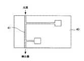
その一方で、図6に示すように、光源からの光をマイクロチップの一方の側面から入射させて、マイクロチップ40内の検出用流路41に充填された検体によって光吸収させ、他方の側面から出てくる蛍光を検出するという技術が、特開2004−77305号公報に記載されている。マイクロチップの直線状の検体の検出用流路を使用する方法において、検体として血液を用いて吸光度を測定すれば精度良く測定できるものと考えられる。 On the other hand, as shown in FIG. 6, the light from the light source is incident from one side surface of the microchip and is absorbed by the specimen filled in the
吸光光度法によって試料の濃度を測定するのにマイクロチップを使用する場合、光路長は、吸収量を稼ぐ必要性から短く出来ないので、吸光度測定部の光入出射部分の面積は例えば0.49mm2と非常に小さく、非常に細長いセルにする必要がある。そのため正確な吸光度測定には平行度の高い光を入射させる必要がある。光の平行度が高ければ、吸光度測定部側面を通過して吸光度測定部外部に漏れる光が減少し、迷光による測定誤差が小さくなるからである。ここで迷光というのは、吸光度測定部以外のチップ部分を通過して光検出器に入り込む光である。When a microchip is used to measure the concentration of a sample by absorptiometry, the optical path length cannot be shortened due to the need to increase the amount of absorption, so the area of the light incident / exit portion of the absorbance measurement unit is, for example, 0.49 mmIt is necessary to make the cells very small as2 and very elongated. For this reason, it is necessary to make incident light with high parallelism for accurate absorbance measurement. This is because if the parallelism of light is high, the light that passes through the side surface of the absorbance measurement unit and leaks to the outside of the absorbance measurement unit is reduced, and the measurement error due to stray light is reduced. Here, the stray light is light that passes through the chip portion other than the absorbance measurement unit and enters the photodetector.
理想的な光源としてはレーザーが考えられるが、化学分析に必要な波長は多岐に亘っており、単色光であるレーザーは必要な波長毎に別のレーザーを必要とし、またコスト的にも高価となり、不適である。あるいは必要な波長を放射するレーザーが存在しないことも考えられる。よって光源には、連続波長域の光を放射するキセノンランプ等の放電ランプと波長選択フィルタなどの波長選択手段と組み合わせた構成の光源が好ましい。 Lasers can be considered as ideal light sources, but there are a wide range of wavelengths required for chemical analysis, and monochromatic lasers require separate lasers for each required wavelength, and are also expensive in cost. Is unsuitable. It is also conceivable that there is no laser emitting the necessary wavelength. Therefore, a light source having a configuration in which a discharge lamp such as a xenon lamp that emits light in a continuous wavelength region and wavelength selection means such as a wavelength selection filter is combined is preferable.
しかし、放電ランプは発光点が大きく平行光を効率よく放射できないので、吸光度測定部以外の部分を通って受光器に入る迷光対策が必要となる。迷光は測定値に影響を与えるからである。 However, since the discharge lamp has a large light emitting point and cannot emit parallel light efficiently, it is necessary to take measures against stray light that enters the light receiver through a portion other than the absorbance measurement unit. This is because stray light affects the measured value.
なお、平行度の低い光をマイクロチップの吸光度測定部に入射させる際の工夫として、吸光度測定部内部をフッ素系樹脂やアルミニウムなどでコーティングし、全反射を利用して光を出口まで導くという方法がある。また、吸光度測定部端面に石英材を貼り付け、基板を測定波長に対して不透明なものにするという方法もある。
吸光度測定部に導光する手段としては、チップの溝に光ファイバーを差し込み、セル内部では全反射を利用する方法がある。
As a means for guiding light to the absorbance measurement unit, there is a method in which an optical fiber is inserted into the groove of the chip and total reflection is used inside the cell.
吸光度測定部内部をコーティングする方法では、吸光度測定部端面に対して斜めに入射した光は内部で全反射して受光器に届くため、吸光度測定部の長さよりも光路が長くなり実際よりも透過率が低くなるので、正しい透過率が測定できない。端面以外の部分を不透明にする方法では、全反射臨界角よりも浅い角度で吸光度測定部の側面に当たった光が全反射し、吸光度測定部の長さよりも光路が長くなり実際よりも透過率が低くなるので、測定誤差の要因になってしまう。光ファイバーを用いて導光する方法では、ファイバー先端から出た光が広がってしまうので吸光度測定部内部で反射が生じ測定値に誤差が生じてしまう恐れがある。 In the method of coating the inside of the absorbance measurement unit, the light incident obliquely to the end surface of the absorbance measurement unit is totally reflected internally and reaches the light receiver, so that the optical path is longer than the length of the absorbance measurement unit and is actually transmitted. Since the rate is low, the correct transmittance cannot be measured. In the method of making the part other than the end face opaque, the light hitting the side surface of the absorbance measurement unit at an angle shallower than the total reflection critical angle is totally reflected, the optical path becomes longer than the length of the absorbance measurement unit, and the transmittance is higher than the actual transmittance. Becomes a factor of measurement error. In the method of guiding light using an optical fiber, the light emitted from the tip of the fiber spreads, so that reflection may occur inside the absorbance measurement unit, resulting in an error in the measurement value.
そこで、本発明の目的は、放電ランプを測定用光源に使用してマイクロチップの吸光度測定を行っても、測定誤差が少ない測定を可能にするマイクロチップを使った吸光度測定ユニットを提供することにある。 Accordingly, an object of the present invention is to provide an absorbance measurement unit using a microchip that enables measurement with little measurement error even when the absorbance of the microchip is measured using a discharge lamp as a measurement light source. is there.
上記課題を解決するために、請求項1に記載の発明は、貼り合わせた板部材からなり、貼り合わせ面に空洞部を有し、該空洞部が連通して分析液導入部と試薬溜まり部と試薬混合部と該板部材の一端面に沿って直線状に配設される吸光度測定部を構成し備えてなるマイクロチップと、該マイクロチップを組み込むチップホルダとからなるマイクロチップを使った吸光度測定ユニットにおいて、該チップホルダには、該吸光度測定部と光軸を一致し、該吸光度測定部の光軸に垂直な断面径よりも狭い開口径を有する、該吸光度測定部へ光導入するための空洞よりなり、内面が非反射処理されてなるキャピラリー部が形成され、該キャピラリー部の光軸に垂直な最大長さをD1、キャピラリー部の光軸方向の長さをL1とし、前記吸光度測定部の光軸に垂直な最大長さをD2、マイクロチップの、前記吸光度測定部を含み該吸光度測定部の光軸方向の端面間の距離をL2とするとき、D1<D2であって、D1/L1≦(D2−D1)/2L2であることを特徴とする。
In order to solve the above-mentioned problem, the invention described in claim 1 is composed of a bonded plate member, and has a cavity portion on the bonding surface, and the cavity portion communicates with the analysis solution introducing portion and the reagent reservoir portion. Absorbance using a microchip comprising a microchip comprising an absorbance measuring unit arranged linearly along one end face of the plate member, a reagent mixing unit, and a chip holder incorporating the microchip In the measurement unit, for the purpose of introducing light into the absorbance measurement unit, the tip holder has an optical axis that coincides with the optical axis and has an opening diameter narrower than a cross-sectional diameter perpendicular to the optical axis of the absorbance measurement unit. A capillary part formed bynon-reflecting the inner surface is formed, the maximum length perpendicular to the optical axis ofthe capillary partis D1, and thelength ofthe capillary part in the optical axis direction is L1, Absorbance measurement unit D2perpendicular maximum length to the opticalaxis,of the microchip, the distance between the end faces of the optical axis of the absorbance measuring unit includes the absorbance measurement unitwhen theL2,aD 1<D2characterized in that itis aD 1 / L 1 ≦ (D 2 -D 1) / 2L 2.
請求項2に記載の発明は、請求項1に記載の発明において、前記チップホルダはアルミニウム製であり、前記キャピラリー部内面を黒アルマイト処理されてなることを特徴とする。
The invention of claim 2 isthe invention according to claim 1, wherein the chip holder is made of aluminum, and wherein the Rukotosuch the capillary inner surface are black anodized.
請求項3に記載の発明は、請求項1または2に記載の発明において、前記キャピラリー部は内部に拡径部を有することを特徴とする。
The invention of claim 3 isthe invention according to claim 1 or 2, wherein the capillary unit is characterized Rukototo have a enlarged diameter portion therein.
また、請求項4に記載の発明は、請求項1乃至3のいずれかに記載の発明において、前記チップホルダは、マイクロチップを挟む2つの部材からなり、一方あるいは両方の部材内面に溝が形成され、2つの部材を合わせることでキャピラリー部を形成することを特徴とする。
The invention according to claim 4 is the invention according toany one of claims 1 to 3, wherein the chip holder includes two members sandwiching the microchip, and a groove is formed on the inner surface of one or both members. The capillary member is formed by combining the two members .
そして、請求項5に記載の発明は、請求項1乃至4のいずれかに記載の発明において、前記チップホルダは前記マイクロチップを該チップホルダに嵌め込むことで該チップホルダのキャピラリー部と該マイクロチップの吸光度測定部との光軸が一致するものであって、該マイクロチップは該チップホルダに弾性部材により押さえられ保持されるものであることを特徴とする。
According to a fifth aspect of the present invention, in the invention according toany one of the first to fourth aspects, the chip holder fits the microchip into the chip holder so that the capillary portion of the chip holder and the micro The optical axis coincides with the absorbance measurement unit of the chip, and the microchip is held and held by the chip holder by an elastic member .
請求項1の発明によれば、キャピラリー部を通過して吸光度測定部に入射する光は平行光成分が多く、吸光度測定精度をキャピラリー部を使用しない場合に比べ上げることが出来る。 According to the first aspect of the present invention, the light that passes through the capillary part and enters the absorbance measurement unit has many parallel light components, and the absorbance measurement accuracy can be increased as compared with the case where the capillary unit is not used.
請求項2および請求項3の発明によれば、キャピラリー部内部で反射する光をなくすことで、平行光成分を多くすることができ、吸光度測定精度をキャピラリー部の不使用の場合に比べ上げることが出来る。 According to the invention of claim 2 and claim 3, by eliminating the light reflected inside the capillary part, the parallel light component can be increased, and the absorbance measurement accuracy can be increased as compared with the case where the capillary part is not used. I can do it.
請求項4の発明によれば、キャピラリー部内部で反射する光をほぼ完全になくすことが出来る。 According to the invention of claim 4, the light reflected inside the capillary portion can be almost completely eliminated.
請求項5の発明によれば、吸光度測定部入射口前面のキャピラリーを通過した光は必ず試料中を進み、吸光度測定部の側面に当たることなく検出器に到達する。よって、誤差なく精度の良い吸光度測定が行える。 According to the fifth aspect of the present invention, the light that has passed through the capillary in front of the absorbance measurement unit entrance always travels through the sample and reaches the detector without hitting the side surface of the absorbance measurement unit. Therefore, accurate absorbance measurement can be performed without error.
請求項6の発明によれば、キャピラリー部をチップホルダ内に簡便に形成することが出来る。According to the invention of claim 6, the capillary part can be easily formed in the chip holder.
請求項7の発明によれば、マイクロチップをチップホルダに嵌め込むことでチップホルダのキャピラリー部とマイクロチップの吸光度測定部との光軸が一致させ、マイクロチップはチップホルダに弾性部材により押さえられ保持され、チップホルダからマイクロチップが抜けることがなく、安定した吸光度測定ができる。 According to the invention of claim 7, by inserting the microchip into the chip holder, the optical axes of the capillary part of the chip holder and the absorbance measuring part of the microchip are matched, and the microchip is held by the chip holder by the elastic member. The microchip is not removed from the chip holder, and stable absorbance measurement can be performed.
図4に本発明の吸光度測定ユニットに使用されるマイクロチップ10の一構成例を示す。マイクロチップ10はPMMA(ポリメタクリル酸メチル)、PET(ポリエチレンテレフタレート)、PC(ポリカーボネート)等の熱可塑性樹脂やエポキシ樹脂などの熱硬化性樹脂等のプラスチック材料からなる。マイクロチップ10は、2枚の板部材が貼り合わされてできている。貼りあわせ面の片面に予め溝が形成され、貼りあわせることで溝が空洞を形成する。そしてチップ外部と連通し分析液をチップに導入する分析液導入部11と分析液と反応させるための試薬を充填した試薬溜まり部12と分析液と試薬を混合する試薬混合部13と混合して出来た検査液に外部から光を通過させる吸光度測定部14を備える。吸光度測定部14は板部材の一端面に沿って直線状に配設されている。なお、図4においては試薬溜まり部12、試薬混合部13、吸光度測定部14等は、マイクロチップ10内部にあるが便宜上実線で表記している。 FIG. 4 shows one configuration example of the
図1には本発明のマイクロチップ用の吸光度測定ユニットを示す。図1(a)には、マイクロチップ10をチップホルダ20に嵌め込んだ状態を示す。チップホルダ10は図1(a)のA−A´断面図である図1(b)に示すように、2つ割りの部材からなり、一方の内面に直線状の溝が形成されており、2つのチップホルダ部材201と202を合わせることにより、図1(b)のようなキャピラリー部21が形成されることになる。このように、2つの部材を合わせることにより、キャピラリー部21をチップホルダ20内に簡便に形成することが出来る。なお、2つ割りの部材の両方に直線状の溝を形成することもできる。 FIG. 1 shows an absorbance measurement unit for a microchip according to the present invention. FIG. 1A shows a state in which the
図9にチップホルダの概略の斜視図を示す。チップホルダ20はマイクロチップ(不図示)をチップホルダ20に矢印の方向に嵌め込むことで、マイクロチップはチップホルダ内壁20a、20bと突き当たることで、位置決めされ、チップホルダ20のキャピラリー部21とマイクロチップの吸光度測定部との光軸が一致する。そして、マイクロチップ10は図1(b)に示すようにチップホルダ20に弾性部材22により押さえられ保持される。弾性部材は具体的にはたとえば板バネであり、あるいはゴム部材などが使用できる。なお、図9で記号42は受光器用光取出部である。 FIG. 9 shows a schematic perspective view of the chip holder. The
キャピラリー部21の開口径は吸光度測定部の光軸に垂直な断面の径より狭い径になっている。一例を挙げれば、キャピラリー部の開口径は0.3mm角、吸光度測定部の光軸に垂直な断面の径は0.7mm角である。また、キャピラリー部の光軸は吸光度測定部の光軸と一致している。キャピラリー部に入る光は後述するが、フィルタで選別された光であり、キャピラリー部を通って吸光度測定部に入り、フォトダイオード等の受光素子で受光される。キャピラリー部を通過して吸光度測定部に入射する光は平行光成分が多く、吸光度の測定の精度を上げる。 The opening diameter of the
また、キャピラリー部内部に、例えばキャピラリー部内面がアルミニウムからなるものであれば黒アルマイト処理を施すと、キャピラリー部内で反射する光が減少し平行度の高い光を吸光度測定部に導くことができる。 Further, if the inside of the capillary portion is made of aluminum, for example, if the inner surface of the capillary portion is made of aluminum, the light reflected in the capillary portion is reduced and light with high parallelism can be guided to the absorbance measuring portion.
さらには、図7のようにキャピラリー部21内部に拡径部21aを有するようにすると、例えばキャピラリー中央部を窪ませた形状にすることで、キャピラリー部内部で反射する光を完全に抑えることができる。 Furthermore, when the enlarged-diameter portion 21a is provided inside the
図2はキャピラリー部と吸光度測定部と受光器の関係を説明する図である。キャピラリー部の光軸に垂直な最大長さをD1、キャピラリー部の光軸方向の長さをL1とし、前記吸光度測定部の光軸に垂直な最大長さをD2、マイクロチップの、前記吸光度測定部を含み該吸光度測定部の光軸方向の端面間の距離をL2とするとき、D1<D2であって、
D1/L1≦(D2−D1)/2L2という関係式を満たすとき、吸光度測定部内側面に当たる光はなくなり、受光器には、吸光度測定部を通過した光のみが入射することで測定精度がさらに上がる。
FIG. 2 is a diagram illustrating the relationship among the capillary section, the absorbance measurement section, and the light receiver. The maximum length perpendicular to the optical axis of the capillary part is D1 , the length of the capillary part in the optical axis direction is L1 , the maximum length perpendicular to the optical axis of the absorbance measurement part is D2 , When the distance between the end faces in the optical axis direction of the absorbance measurement unit including the absorbance measurement unit is L2 , D1 <D2 and
When satisfyingD 1 / L1 ≦ (D 2 -D 1) / 2L 2 that relationship, light impinging on theabsorbance measurement portion side is no longer, the photodetector, the measurement by only the light passing through themeasuring absorbance is incident The accuracy further increases.
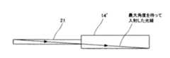
図3はキャピラリー部端部から入射した光が吸光度測定部を通過する様子を示す。
この図3の状態はD1/L1=(D2−D1)/2L2の関係のときのものである。
キャピラリー部端部から吸光度測定部に入射した光線において、最大角度を持って入射した光線は、吸光度測定部の内部で反射することなく、吸光度測定部の端部まで到達している。
FIG. 3 shows how the light incident from the end of the capillary passes through the absorbance measurement unit.
The state shown in FIG. 3 corresponds to the relationship D1 / L1 = (D2 −D1 ) / 2L2 .
In light rays incident to theabsorbance measurement unit from the capillary portion end, light rays incident at a maximum angle without being reflected insidethe measuring absorbance has reached to the end of the absorbance measurement unit.
図5は上式に関して、効果を検証するために行った測定実験の結果を示す。
図1における吸光度測定ユニットに、吸光度測定部に純水、5-アミノ-2-ニトロ安息香酸溶液(1、5、10、20、30、50μmol/L)の7種の溶液を各々充填し、図8に示した測定系を組み、キセノンランプ30とレンズ31とバンドパスフィルタ32を組み合わせた光源から中心波長405nmの光(405±5nm)をキャピラリー部21から入射させて、吸光度測定部14を通過後の光をシリコンフォトダイオードからなる受光器33で受光して、その減衰割合を調べたものである。すなわち、純水のみを吸光度測定部に入れたときの光の到達量を100%として受光器33にどの程度減衰して到達するかその到達量を見ている。5-アミノ-2-ニトロ安息香酸溶液は波長405nm付近に吸収を持ち、その濃度によって吸収量が変化する。図中のプロットは吸光度測定部14を通過後の光をシリコンフォトダイオードからなる受光器33で受光したときの到達量の値である。その値の近似直線が図中の実線である。なお、図5で標準値とは中心波長405nmの光(405±5nm)を、上記の純水、5-アミノ-2-ニトロ安息香酸溶液(1、5、10、20、30、50μmol/L)の7種の溶液を透過させて分光光度計で別途測定した値であり、図中点線で示される。FIG. 5 shows the result of a measurement experiment conducted to verify the effect with respect to the above equation.
In the absorbance measurement unit in FIG. 1, the absorbance measurement unit was filled with 7 types of solutions of pure water and 5-amino-2-nitrobenzoic acid solution (1, 5, 10, 20, 30, 50 μmol / L), The measurement system shown in FIG. 8 is assembled, light having a central wavelength of 405 nm (405 ± 5 nm) is incident from the
図5(a)は吸光度測定部の光軸に垂直な最大長さD2が0.7mm、マイクロチップの、前記吸光度測定部を含み該吸光度測定部の光軸方向の端面間の距離L2が10mm、キャピラリー部の光軸に垂直な最大長さをD1が0.5mm、光軸方向の長さをL1が10mmのとき、すなわちD1<D2の場合であって、D1/L1>(D2−D1)/2L2 という関係にある場合である。マイクロチップの吸光度測定部を挟む両側のチップ構成部材の部分は各々1mmある。FIG. 5A shows a distance L2 between the end faces in the optical axis direction of the absorbance measuring section including the absorbance measuring section of a microchip having a maximum length D2 perpendicular to the optical axis of the absorbance measuring section of 0.7 mm. Is 10 mm, the maximum length perpendicular to the optical axis of the capillary section is D1 is 0.5 mm, and the length in the optical axis direction is L1 is 10 mm, that is, D1 <D2 , where D1 This is a case where / L1 > (D2 −D1 ) / 2L2 . The portions of the chip constituent members on both sides sandwiching the absorbance measuring portion of the microchip are each 1 mm.
そして、図5(b)は本願発明であり、吸光度測定部の光軸に垂直な最大長さD2が0.7mm、マイクロチップの、前記吸光度測定部を含み該吸光度測定部の光軸方向の端面間の距離L2が10mm、キャピラリー部の光軸に垂直な最大長さをD1が0.3mm、光軸方向の長さをL1が15mmのとき、すなわちD1<D2の場合であって、D1/L1=(D2−D1)/2L2という関係にある場合である。
図5(b)では、各試薬とも標準値(分光光度計による測定値)とほぼ同様の光減衰割合を示す。図5(a)では、迷光によって標準値よりも光減衰割合が高い結果となった。
Then, FIG. 5 (b) is a present invention, the maximum perpendicular to the optical axis of the absorbance measuring unit length D2 is 0.7 mm, the microchip, the optical axis of the absorbance measuring unit includes the absorbance measurement unit When the distance L2 between the end faces of the optical fiber is 10 mm, the maximum length perpendicular to the optical axis of the capillary portion is D1 is 0.3 mm, and the length in the optical axis direction is L1 is15 mm, that is, D1 <D2 in which D1 / L1= (D2 −D1 ) / 2L2 .
In FIG.5 (b), each reagent shows the light attenuation rate substantially the same as a standard value (measurement value by a spectrophotometer). In FIG. 5A, the light attenuation ratio was higher than the standard value due to stray light.
以上のことから、吸光度測定部の光軸に垂直な最大長さをD2、マイクロチップの、前記吸光度測定部を含み該吸光度測定部の光軸方向の端面間の距離をL2、キャピラリー部の光軸に垂直な最大長さをD1、光軸方向の長さをL1とするとき、
D1<D2であって、D1/L1≦(D2−D1)/2L2とすることで、精度良く吸光度を測定することができることが確認された。From the above, the maximum length perpendicular to the optical axis of the absorbance measurement unit is D2 , the distance between the end faces in the optical axis direction of the absorbance measurement unit including the absorbance measurement unit is L2 , and the capillary unit When the maximum length perpendicular to the optical axis is D1 and the length in the optical axis direction is L1 ,
It was confirmed that D1 <D2 and D1 / L1 ≦ (D2 −D1 ) / 2L2 can be measured with high accuracy.
10 マイクロチップ
11 分析液導入部
12 試薬溜まり部
13 試薬混合部
14 吸光度測定部
14´ 吸光度測定部を含むチップ部位
20 チップホルダ
20a、20b チップホルダ内壁
201、202 チップホルダ部材
21 キャピラリー部
21a 拡径部
22 弾性部材
30 キセノンランプ
31 レンズ
32 バンドパスフィルタ
33 受光器
40 マイクロチップ
41 検出用流路
42 受光器用光取出部
DESCRIPTION OF
Claims (5)
Translated fromJapanese貼り合わせ面に空洞部を有し、該空洞部が連通して分析液導入部と試薬溜まり部と試薬混合部と該板部材の一端面に沿って直線状に配設される吸光度測定部を構成し備えてなるマイクロチップと、
該マイクロチップを組み込むチップホルダとからなるマイクロチップを使った吸光度測定ユニットにおいて、
該チップホルダには、該吸光度測定部と光軸を一致し、該吸光度測定部の光軸に垂直な断面径よりも狭い開口径を有する、該吸光度測定部へ光導入するための空洞よりなり、内面が非反射処理されてなるキャピラリー部が形成され、
該キャピラリー部の光軸に垂直な最大長さをD1、キャピラリー部の光軸方向の長さをL1とし、前記吸光度測定部の光軸に垂直な最大長さをD2、マイクロチップの、前記吸光度測定部を含み該吸光度測定部の光軸方向の端面間の距離をL2とするとき、D1<D2であって、D1/L1≦(D2−D1)/2L2であることを特徴とする吸光度測定ユニット。Consists of bonded plate members,
An absorptivity measuring unit that has a cavity on the bonding surface, and that communicates with the cavity and is linearly arranged along one end surface of the plate member, the analysis solution introduction unit, the reagent reservoir, the reagent mixing unit A microchip configured and provided;
In an absorbance measurement unit using a microchip consisting of a chip holder incorporating the microchip,
The on chip holder is to match the absorbance measurement unit and the optical axis, with a narrow opening diameter than a cross-section perpendicular diameter to the optical axis of the absorbance measuring unitconsists of a cavity for introducing light into the absorbance measuring unit, A capillary part formed by thenon-reflection treatment of the inner surface is formed,
The maximum length perpendicular to the optical axis ofthe capillary partis D1, thelength ofthe capillary part in the optical axis direction is L1, the maximum length perpendicular to the optical axis of the absorbance measurement part is D2, When the distance between the end faces in the optical axis direction of the absorbance measuring unit including the absorbance measuring unit is L2, D1<D2and D1/ L1≦ (D2−D1) /absorbance measurement unit, which is a2L2.
Priority Applications (6)
| Application Number | Priority Date | Filing Date | Title |
|---|---|---|---|
| JP2004274788AJP4506375B2 (en) | 2004-09-22 | 2004-09-22 | Absorbance measurement unit |
| TW094121909ATW200610953A (en) | 2004-09-22 | 2005-06-29 | Absorbance measuring unit |
| EP05019661AEP1640704B1 (en) | 2004-09-22 | 2005-09-09 | Unit for measuring absorbance |
| DE602005006490TDE602005006490D1 (en) | 2004-09-22 | 2005-09-09 | Unit for measuring absorption |
| US11/225,044US7901631B2 (en) | 2004-09-22 | 2005-09-14 | Unit for measuring absorbance |
| CNB2005101068125ACN100538332C (en) | 2004-09-22 | 2005-09-22 | Absorbance measurement unit |
Applications Claiming Priority (1)
| Application Number | Priority Date | Filing Date | Title |
|---|---|---|---|
| JP2004274788AJP4506375B2 (en) | 2004-09-22 | 2004-09-22 | Absorbance measurement unit |
Publications (2)
| Publication Number | Publication Date |
|---|---|
| JP2006090775A JP2006090775A (en) | 2006-04-06 |
| JP4506375B2true JP4506375B2 (en) | 2010-07-21 |
Family
ID=35462330
Family Applications (1)
| Application Number | Title | Priority Date | Filing Date |
|---|---|---|---|
| JP2004274788AExpired - Fee RelatedJP4506375B2 (en) | 2004-09-22 | 2004-09-22 | Absorbance measurement unit |
Country Status (6)
| Country | Link |
|---|---|
| US (1) | US7901631B2 (en) |
| EP (1) | EP1640704B1 (en) |
| JP (1) | JP4506375B2 (en) |
| CN (1) | CN100538332C (en) |
| DE (1) | DE602005006490D1 (en) |
| TW (1) | TW200610953A (en) |
Families Citing this family (5)
| Publication number | Priority date | Publication date | Assignee | Title |
|---|---|---|---|---|
| JP4912096B2 (en)* | 2006-09-07 | 2012-04-04 | ローム株式会社 | Microchip inspection device |
| EP2307559B1 (en)* | 2008-03-03 | 2015-09-02 | Imigene, Inc. | Infection mediated foam dissolution rate measurement |
| EP2124036A1 (en)* | 2008-05-20 | 2009-11-25 | Agilent Technologies, Inc. | Pre-positioning and guiding mechanism for inserting a flow cell in a detector |
| US8654323B2 (en)* | 2010-09-27 | 2014-02-18 | Arkray, Inc. | Analyzing apparatus |
| JP2015118043A (en)* | 2013-12-19 | 2015-06-25 | ブラザー工業株式会社 | Inspection device |
Family Cites Families (17)
| Publication number | Priority date | Publication date | Assignee | Title |
|---|---|---|---|---|
| JPH0197841A (en)* | 1987-10-09 | 1989-04-17 | Hitachi Ltd | Absorptiometer |
| US5013155A (en)* | 1989-09-26 | 1991-05-07 | Chemetrics, Inc. | Portable spectrophotometric instrument having vial holder and light integrator |
| US6399023B1 (en)* | 1996-04-16 | 2002-06-04 | Caliper Technologies Corp. | Analytical system and method |
| JPH1137931A (en)* | 1997-07-14 | 1999-02-12 | Tokimec Inc | Spectrophotometer |
| JP2004239611A (en)* | 1999-10-12 | 2004-08-26 | Nok Corp | Co sensor |
| US20030091477A1 (en)* | 1999-12-22 | 2003-05-15 | Paul Eric A. | Flow-thru chip cartridge, chip holder, system & method thereof |
| JP3969699B2 (en)* | 2000-11-17 | 2007-09-05 | 日本板硝子株式会社 | Chip member for microchemical system, and microchemical system using the chip member |
| JP2002221485A (en)* | 2000-11-22 | 2002-08-09 | Minolta Co Ltd | Micro chip |
| CA2468260A1 (en)* | 2001-07-02 | 2003-01-16 | Matthew Torres | Flow-thru chip cartridge, chip holder, system & method thereof |
| JP2003207454A (en)* | 2002-01-15 | 2003-07-25 | Minolta Co Ltd | Transmission light-detecting apparatus |
| JP3761475B2 (en)* | 2002-02-28 | 2006-03-29 | 国際技術開発株式会社 | Sample cartridge and sample analyzer |
| JP2003279471A (en)* | 2002-03-20 | 2003-10-02 | Nippon Sheet Glass Co Ltd | Chip for microchemical system and microchemical system |
| JP2004077305A (en)* | 2002-08-19 | 2004-03-11 | Nec Corp | Detector |
| JP2004109099A (en) | 2002-09-16 | 2004-04-08 | Jun Kikuchi | Method of analyzing blood, apparatus for analyzing blood, and method of manufacturing apparatus for analyzing blood |
| JP4375183B2 (en)* | 2004-09-22 | 2009-12-02 | ウシオ電機株式会社 | Microchip |
| JP4626276B2 (en)* | 2004-11-18 | 2011-02-02 | ウシオ電機株式会社 | Microchip inspection device |
| JP4912096B2 (en)* | 2006-09-07 | 2012-04-04 | ローム株式会社 | Microchip inspection device |
- 2004
- 2004-09-22JPJP2004274788Apatent/JP4506375B2/ennot_activeExpired - Fee Related
- 2005
- 2005-06-29TWTW094121909Apatent/TW200610953A/ennot_activeIP Right Cessation
- 2005-09-09DEDE602005006490Tpatent/DE602005006490D1/ennot_activeExpired - Lifetime
- 2005-09-09EPEP05019661Apatent/EP1640704B1/ennot_activeExpired - Lifetime
- 2005-09-14USUS11/225,044patent/US7901631B2/ennot_activeExpired - Fee Related
- 2005-09-22CNCNB2005101068125Apatent/CN100538332C/ennot_activeExpired - Fee Related
Also Published As
| Publication number | Publication date |
|---|---|
| TWI334925B (en) | 2010-12-21 |
| CN1752740A (en) | 2006-03-29 |
| EP1640704B1 (en) | 2008-05-07 |
| CN100538332C (en) | 2009-09-09 |
| EP1640704A3 (en) | 2006-06-07 |
| DE602005006490D1 (en) | 2008-06-19 |
| US7901631B2 (en) | 2011-03-08 |
| TW200610953A (en) | 2006-04-01 |
| EP1640704A2 (en) | 2006-03-29 |
| US20060061759A1 (en) | 2006-03-23 |
| JP2006090775A (en) | 2006-04-06 |
Similar Documents
| Publication | Publication Date | Title |
|---|---|---|
| US8289511B2 (en) | Light-guiding flowcells with minimal stray light | |
| US9778184B2 (en) | Measurement method and measurement device | |
| US8502969B2 (en) | Miniature flow-through cuvette and spectrophotometer containing the same | |
| WO2010010904A1 (en) | Microchip and analyzing apparatus | |
| WO2003078979A1 (en) | Micro-chemical system-use chip and mico-chemical system | |
| JP5802499B2 (en) | Analysis equipment | |
| JP4506375B2 (en) | Absorbance measurement unit | |
| US11644408B2 (en) | Optical cell and methods of manufacturing an optical cell | |
| WO2014038399A1 (en) | Measurement instrument, and measurement apparatus | |
| CN102128809B (en) | Surface plasma resonance sensor chip assembly and cylindrical prism chip | |
| KR101970689B1 (en) | Flow cytometry using optical fiber | |
| JP4626276B2 (en) | Microchip inspection device | |
| US20070081159A1 (en) | Apparatus and methods for evaluating an optical property of a liquid sample | |
| US10775307B2 (en) | Optical fiber fluorescence detection device | |
| CN1216281C (en) | Micro-analysis chip for absorbance photometric detection and method of use thereof | |
| JP2003130826A (en) | Method for photothermal spectroscopic analysis, and micro-chemical system | |
| US20140099703A1 (en) | Capillary Waveguide Cuvette | |
| US7277167B2 (en) | Modular cuvettes and methods for use thereof | |
| KR20140034733A (en) | Sample receiving apparatus | |
| JP2004085506A (en) | Micro-chemical analyzer | |
| JP2005091093A (en) | Microchip for measuring absorbance | |
| US20090145201A1 (en) | Methods and apparatuses for reducing effects of molecule adsorption within microfluidic channels | |
| JP4411752B2 (en) | Well plate | |
| CN114174801A (en) | Detector for liquid chromatograph |
Legal Events
| Date | Code | Title | Description |
|---|---|---|---|
| A621 | Written request for application examination | Free format text:JAPANESE INTERMEDIATE CODE: A621 Effective date:20070306 | |
| RD04 | Notification of resignation of power of attorney | Free format text:JAPANESE INTERMEDIATE CODE: A7424 Effective date:20090119 | |
| A131 | Notification of reasons for refusal | Free format text:JAPANESE INTERMEDIATE CODE: A131 Effective date:20100126 | |
| A521 | Request for written amendment filed | Free format text:JAPANESE INTERMEDIATE CODE: A523 Effective date:20100224 | |
| TRDD | Decision of grant or rejection written | ||
| A01 | Written decision to grant a patent or to grant a registration (utility model) | Free format text:JAPANESE INTERMEDIATE CODE: A01 Effective date:20100406 | |
| A01 | Written decision to grant a patent or to grant a registration (utility model) | Free format text:JAPANESE INTERMEDIATE CODE: A01 | |
| A61 | First payment of annual fees (during grant procedure) | Free format text:JAPANESE INTERMEDIATE CODE: A61 Effective date:20100419 | |
| FPAY | Renewal fee payment (event date is renewal date of database) | Free format text:PAYMENT UNTIL: 20130514 Year of fee payment:3 | |
| R150 | Certificate of patent or registration of utility model | Free format text:JAPANESE INTERMEDIATE CODE: R150 | |
| S111 | Request for change of ownership or part of ownership | Free format text:JAPANESE INTERMEDIATE CODE: R313113 | |
| FPAY | Renewal fee payment (event date is renewal date of database) | Free format text:PAYMENT UNTIL: 20130514 Year of fee payment:3 | |
| R350 | Written notification of registration of transfer | Free format text:JAPANESE INTERMEDIATE CODE: R350 | |
| LAPS | Cancellation because of no payment of annual fees |