JP4501899B2 - Liquid crystal display device and electronic device - Google Patents
Liquid crystal display device and electronic deviceDownload PDFInfo
- Publication number
- JP4501899B2 JP4501899B2JP2006163117AJP2006163117AJP4501899B2JP 4501899 B2JP4501899 B2JP 4501899B2JP 2006163117 AJP2006163117 AJP 2006163117AJP 2006163117 AJP2006163117 AJP 2006163117AJP 4501899 B2JP4501899 B2JP 4501899B2
- Authority
- JP
- Japan
- Prior art keywords
- pixel
- sub
- liquid crystal
- display device
- crystal display
- Prior art date
- Legal status (The legal status is an assumption and is not a legal conclusion. Google has not performed a legal analysis and makes no representation as to the accuracy of the status listed.)
- Active
Links
Images


Classifications
- G—PHYSICS
- G02—OPTICS
- G02F—OPTICAL DEVICES OR ARRANGEMENTS FOR THE CONTROL OF LIGHT BY MODIFICATION OF THE OPTICAL PROPERTIES OF THE MEDIA OF THE ELEMENTS INVOLVED THEREIN; NON-LINEAR OPTICS; FREQUENCY-CHANGING OF LIGHT; OPTICAL LOGIC ELEMENTS; OPTICAL ANALOGUE/DIGITAL CONVERTERS
- G02F1/00—Devices or arrangements for the control of the intensity, colour, phase, polarisation or direction of light arriving from an independent light source, e.g. switching, gating or modulating; Non-linear optics
- G02F1/01—Devices or arrangements for the control of the intensity, colour, phase, polarisation or direction of light arriving from an independent light source, e.g. switching, gating or modulating; Non-linear optics for the control of the intensity, phase, polarisation or colour
- G02F1/13—Devices or arrangements for the control of the intensity, colour, phase, polarisation or direction of light arriving from an independent light source, e.g. switching, gating or modulating; Non-linear optics for the control of the intensity, phase, polarisation or colour based on liquid crystals, e.g. single liquid crystal display cells
- G02F1/133—Constructional arrangements; Operation of liquid crystal cells; Circuit arrangements
- G02F1/1333—Constructional arrangements; Manufacturing methods
- G02F1/1335—Structural association of cells with optical devices, e.g. polarisers or reflectors
- G02F1/133509—Filters, e.g. light shielding masks
- G02F1/133514—Colour filters
- G—PHYSICS
- G02—OPTICS
- G02F—OPTICAL DEVICES OR ARRANGEMENTS FOR THE CONTROL OF LIGHT BY MODIFICATION OF THE OPTICAL PROPERTIES OF THE MEDIA OF THE ELEMENTS INVOLVED THEREIN; NON-LINEAR OPTICS; FREQUENCY-CHANGING OF LIGHT; OPTICAL LOGIC ELEMENTS; OPTICAL ANALOGUE/DIGITAL CONVERTERS
- G02F1/00—Devices or arrangements for the control of the intensity, colour, phase, polarisation or direction of light arriving from an independent light source, e.g. switching, gating or modulating; Non-linear optics
- G02F1/01—Devices or arrangements for the control of the intensity, colour, phase, polarisation or direction of light arriving from an independent light source, e.g. switching, gating or modulating; Non-linear optics for the control of the intensity, phase, polarisation or colour
- G02F1/13—Devices or arrangements for the control of the intensity, colour, phase, polarisation or direction of light arriving from an independent light source, e.g. switching, gating or modulating; Non-linear optics for the control of the intensity, phase, polarisation or colour based on liquid crystals, e.g. single liquid crystal display cells
- G02F1/133—Constructional arrangements; Operation of liquid crystal cells; Circuit arrangements
- G02F1/1333—Constructional arrangements; Manufacturing methods
- G02F1/1335—Structural association of cells with optical devices, e.g. polarisers or reflectors
- G02F1/133553—Reflecting elements
- G02F1/133555—Transflectors
- G—PHYSICS
- G02—OPTICS
- G02F—OPTICAL DEVICES OR ARRANGEMENTS FOR THE CONTROL OF LIGHT BY MODIFICATION OF THE OPTICAL PROPERTIES OF THE MEDIA OF THE ELEMENTS INVOLVED THEREIN; NON-LINEAR OPTICS; FREQUENCY-CHANGING OF LIGHT; OPTICAL LOGIC ELEMENTS; OPTICAL ANALOGUE/DIGITAL CONVERTERS
- G02F2202/00—Materials and properties
- G02F2202/40—Materials having a particular birefringence, retardation
Landscapes
- Physics & Mathematics (AREA)
- Nonlinear Science (AREA)
- Mathematical Physics (AREA)
- Chemical & Material Sciences (AREA)
- Crystallography & Structural Chemistry (AREA)
- General Physics & Mathematics (AREA)
- Optics & Photonics (AREA)
- Liquid Crystal (AREA)
Description
Translated fromJapanese本発明は、各種情報の表示に用いて好適な液晶表示装置に関する。 The present invention relates to a liquid crystal display device suitable for use in displaying various information.
近年、携帯電話や携帯情報端末といった携帯機器等に液晶表示装置が用いられている。このような液晶表示装置では、一つの画素に赤(R)、緑(G)、青(B)(以下、これらの色をそれぞれ単に「R」、「G」、「B」とも記す。)のカラーフィルタをそれぞれ有するサブ画素からなる。このような液晶表示装置では、液晶の複屈折率とセル厚の積で表されるリタデーション値の最適値は、各色のサブ画素で異なる。従って、中間調表示におけるホワイトバランスの調整を行うためには、各色のサブ画素ごとにセル厚を調節するのが理想である。 In recent years, liquid crystal display devices have been used in portable devices such as mobile phones and personal digital assistants. In such a liquid crystal display device, red (R), green (G), and blue (B) (hereinafter, these colors are also simply referred to as “R”, “G”, and “B”, respectively) in one pixel. Sub-pixels each having the color filter. In such a liquid crystal display device, the optimum value of the retardation value represented by the product of the birefringence of the liquid crystal and the cell thickness is different for each color sub-pixel. Therefore, in order to adjust the white balance in the halftone display, it is ideal to adjust the cell thickness for each sub-pixel of each color.
一方、最近では、R、G、Bの3色に加え、さらに透明(W)(以下、単に「W」とも記す)のサブ画素を用いた液晶表示装置が提案されている(例えば特許文献1を参照)。 On the other hand, recently, there has been proposed a liquid crystal display device using sub-pixels of transparent (W) (hereinafter also simply referred to as “W”) in addition to three colors of R, G, and B (for example, Patent Document 1). See).
特許文献1に示す液晶表示装置では、上記のようにホワイトバランスの調整を行うためには、RGBWの4色のサブ画素におけるセル厚を調節する必要が生じる。 In the liquid crystal display device disclosed in
本発明は上記の点に鑑みてなされたものであり、透明(W)のサブ画素を有する液晶表示装置において、ホワイトバランスの調整を行うことを課題とする。 The present invention has been made in view of the above points, and it is an object of the present invention to adjust white balance in a liquid crystal display device having transparent (W) sub-pixels.
本発明の1つの観点では、液晶表示装置は、一対の基板と、RGB及び非着色の4つのサブ画素を有して構成される表示画素と、前記一対の基板の間に挟持され、前記各色のサブ画素ごとにセル厚の異なる液晶層と、を備え、前記RGBの各色のサブ画素は、夫々のリタデーション値が、360nm≦R≦700nm、340nm≦G≦600nm、340nm≦B≦500nmとなる関係を有し、前記非着色のサブ画素は、前記表示画素が所定のホワイトバランスとなるセル厚を有する。 In one aspect of the present invention, a liquid crystal display device is sandwiched between a pair of substrates, a display pixel including four RGB and non-colored sub-pixels, and the pair of substrates, and each of the colors Liquid crystal layers having different cell thicknesses for each of the sub-pixels, and each of the RGB sub-pixels has a retardation value of 360 nm ≦ R ≦ 700 nm, 340 nm ≦ G ≦ 600 nm, 340 nm ≦ B ≦ 500 nm. The non-colored sub-pixels have a cell thickness with which the display pixel has a predetermined white balance.
上記の液晶表示装置は、液晶層を挟持してなる一対の基板より構成される。液晶層は、各色のサブ画素ごとにセル厚が異なる。一つの表示画素は、RGB及び非着色の4つのサブ画素から構成される。前記RGBの各色のサブ画素は、そのリタデーション値が、360nm≦R≦700nm、340nm≦G≦600nm、340nm≦B≦500nmの関係を有している。前記非着色のサブ画素は、前記表示画素が所定のホワイトバランスとなるセル厚を有する。このように、上記の液晶表示装置では、前記非着色透明のサブ画素のセル厚を、前記表示画素が所定のホワイトバランスとなる値、即ち、前記非着色のサブ画素が所定の色度となる値に設定することができ、ユーザにとって所望の白色表示を実現することができる。 The above liquid crystal display device includes a pair of substrates that sandwich a liquid crystal layer. The liquid crystal layer has a different cell thickness for each sub-pixel of each color. One display pixel is composed of four sub-pixels of RGB and non-colored. The retardation values of the RGB sub-pixels have a relationship of 360 nm ≦ R ≦ 700 nm, 340 nm ≦ G ≦ 600 nm, and 340 nm ≦ B ≦ 500 nm. The non-colored sub-pixel has a cell thickness at which the display pixel has a predetermined white balance. Thus, in the above liquid crystal display device, the cell thickness of the non-colored transparent sub-pixel is set to a value at which the display pixel has a predetermined white balance, that is, the non-colored sub-pixel has a predetermined chromaticity. The value can be set to a value, and a desired white display can be realized for the user.
上記の液晶表示装置の一態様では、前記非着色のサブ画素のセル厚は、前記RGBのサブ画素のうち、前記表示画素に占める面積が最も小さい色のサブ画素のセル厚と実質的に等しく設定される。このようにしても、非着色のサブ画素は、表示画素に占める面積が最も小さい色の光を補うことができ、白色表示における色付きを抑えることができる。 In one aspect of the above liquid crystal display device, the cell thickness of the non-colored sub-pixel is substantially equal to the cell thickness of the sub-pixel of the color that has the smallest area in the display pixel among the RGB sub-pixels. Is set. Even in this case, the non-colored sub-pixel can compensate for light having the smallest area occupied by the display pixel, and can suppress coloring in white display.
上記の液晶表示装置の他の一態様では、前記表示画素は、前記RGBのサブ画素のうちの1色のサブ画素と前記非着色のサブ画素の合計面積が、他の2色のサブ画素の各々の面積と略等しく構成され、前記非着色のサブ画素のセル厚は、前記1色のサブ画素のリタデーション値と、前記非着色のサブ画素のリタデーション値とが等しくなる値に設定される。例えば、RGBのサブ画素のうち、Bのサブ画素と非着色のサブ画素の合計面積が、他の2色のサブ画素の各々の面積と略等しく構成されている場合において、白色表示を行うと、Bのサブ画素より出光する光は、他の2色のサブ画素より出光する光と比較して不足する。しかし、本発明では、前記非着色のサブ画素のセル厚は、前記1色のサブ画素のリタデーション値と、前記非着色のサブ画素のリタデーション値とが等しくなる値に設定される。これにより、Wのサブ画素より出光する光は、Bの色の成分が強調され、不足しているBの色の光を補うことができ、Bのサブ画素の面積が小さいことによって発生する白色表示における上述した色付きを抑えることができる。 In another mode of the above liquid crystal display device, the display pixel has a total area of one of the RGB sub-pixels and the non-colored sub-pixel of the other two-color sub-pixels. The cell thickness of each of the non-colored sub-pixels is set to a value that makes the retardation value of the one-color sub-pixel equal to the retardation value of the non-colored sub-pixel. For example, when the total area of B subpixels and non-colored subpixels of RGB subpixels is substantially equal to the area of each of the other two color subpixels, white display is performed. The light emitted from the B sub-pixels is insufficient as compared with the light emitted from the other two-color sub-pixels. However, in the present invention, the cell thickness of the non-colored sub-pixel is set to a value at which the retardation value of the one-color sub-pixel is equal to the retardation value of the non-colored sub-pixel. As a result, the light emitted from the W sub-pixel is emphasized in the B-color component, can compensate for the insufficient B-color light, and is generated by the small area of the B sub-pixel. The above-described coloring in the display can be suppressed.
上記の液晶表示装置の他の一態様では、前記表示画素は、前記RGB及び非着色の各色のサブ画素の面積の比率が2:2:1:1となる構成を有し、前記非着色のサブ画素のセル厚は、前記Bのサブ画素のセル厚と実質的に等しくされる。このようにすることで、非着色のサブ画素は、表示画素に占める面積が最も小さいBの色の光を補うことができる。 In another aspect of the liquid crystal display device, the display pixel has a configuration in which an area ratio of the subpixels of the RGB and non-colored colors is 2: 2: 1: 1, The cell thickness of the sub-pixel is made substantially equal to the cell thickness of the B sub-pixel. In this way, the non-colored sub-pixel can compensate for the light of B color, which has the smallest area occupied by the display pixel.
上記の液晶表示装置の他の一態様では、前記表示画素は、前記4つのサブ画素の各々の面積が略等しくなるように構成され、前記非着色のサブ画素のセル厚は、前記Gのサブ画素のリタデーション値と、前記非着色のサブ画素のリタデーション値とが等しくなる値に設定される。また、上記の液晶表示装置の他の一態様では、前記非着色のサブ画素のセル厚は、前記Gのサブ画素のセル厚と実質的に等しくされる。このような構成によれば、非着色のサブ画素のリタデーション値と、視感度の最も高いGのサブ画素のリタデーション値とがほぼ一致するので、輝度の高い表示を行うことができる。 In another aspect of the liquid crystal display device, the display pixel is configured such that the areas of the four sub-pixels are substantially equal, and the cell thickness of the non-colored sub-pixel is the G sub-pixel. The retardation value of the pixel is set to a value that makes the retardation value of the non-colored sub-pixel equal. In another mode of the above liquid crystal display device, the cell thickness of the non-colored sub-pixel is substantially equal to the cell thickness of the G sub-pixel. According to such a configuration, since the retardation value of the non-colored sub-pixel and the retardation value of the G sub-pixel having the highest visibility are substantially the same, display with high luminance can be performed.
本発明の他の観点では、液晶表示装置は、一対の基板と、RGB及び非着色の4つのサブ画素を有して構成され、前記RGB及び非着色の各サブ画素の面積の比率が2:2:1:1となる構成を有する表示画素と、前記一対の基板の間に挟持され、前記各色のサブ画素ごとにセル厚の異なる液晶層と、を備え、前記R、G、B、非着色の各サブ画素は、夫々のセル厚の大きさをdr、dg、db、dwとすると、dr≧dg≧dw≒db(但し、dr=dw=dbとなることはない)となる関係を有する。 In another aspect of the present invention, a liquid crystal display device includes a pair of substrates and four sub-pixels of RGB and non-colored, and the ratio of the areas of the RGB and non-colored sub-pixels is 2: A display pixel having a configuration of 2: 1: 1 and a liquid crystal layer sandwiched between the pair of substrates and having a different cell thickness for each sub-pixel of each color. Each coloring sub-pixel has a relationship of dr ≧ dg ≧ dw≈db (provided that dr = dw = db is not satisfied) when the cell thicknesses are dr, dg, db, and dw. Have.
上記構成において白色表示を行うと、Bのサブ画素より出光する光は、他の2色、即ちR、Gのサブ画素より出光する光と比較して不足する。しかし、前記非着色のサブ画素のセル厚が、Bのサブ画素のセル厚と略等しくなっていることにより、これらのサブ画素におけるリタデーション値が略等しくなるため、非着色のサブ画素より出光する光は、Bの色の成分が強調され、不足しているBの色の光を補うことができる。よって、Bのサブ画素の面積が小さいことによって発生する白色表示における上述した色付きを抑えることができる。即ち、非着色のサブ画素は、表示画素に占める面積が最も小さいBのサブ画素より出光する光の色を補うことができる。 When white display is performed in the above configuration, the light emitted from the B subpixel is insufficient as compared with the light emitted from the other two colors, that is, the R and G subpixels. However, since the cell thickness of the non-colored sub-pixel is substantially equal to the cell thickness of the B sub-pixel, the retardation values in these sub-pixels are approximately equal, and therefore light is emitted from the non-colored sub-pixel. The light has a B color component emphasized, and can compensate for the lack of B light. Therefore, it is possible to suppress the above-described coloring in white display that occurs when the area of the B sub-pixel is small. That is, the non-colored sub-pixel can supplement the color of light emitted from the B sub-pixel having the smallest area occupied by the display pixel.
本発明の他の観点では、液晶表示装置は、一対の基板と、RGB及び非着色の4つのサブ画素から構成される表示画素と、前記一対の基板の間に挟持され、前記各色のサブ画素ごとにセル厚の異なる液晶層と、を備え、前記R、G、B、非着色の各サブ画素は、夫々のセル厚の大きさをdr、dg、db、dwとすると、dr≧dw≒dg≧db(但し、dr=dw=dbとなることはない)となる関係を有する。この場合において、前記表示画素は、前記RGB及び非着色の各サブ画素の面積の比率が1:1:1:1となる構成を有することが好ましい。 In another aspect of the present invention, a liquid crystal display device includes a pair of substrates, a display pixel composed of four sub-pixels of RGB and non-coloring, and a sub-pixel of each color sandwiched between the pair of substrates. And each of the R, G, B, and non-colored sub-pixels has a cell thickness of dr, dg, db, dw, and dr ≧ dw≈ dg ≧ db (provided that dr = dw = db is not satisfied). In this case, it is preferable that the display pixel has a configuration in which an area ratio of the RGB and non-colored sub-pixels is 1: 1: 1: 1.
上記の液晶表示装置は、液晶層を挟持してなる一対の基板より構成される。液晶層は、各色のサブ画素ごとにセル厚が異なる。一つの表示画素は、RGB及び非着色の4つのサブ画素から構成される。R、G、B、非着色の各サブ画素は、夫々のセル厚の大きさをdr、dg、db、dwとすると、dr≧dw≒dg≧db(但し、dr=dw=dbとなることはない)となる関係を有する。このように、視感度の最も高いGのセル厚とほぼ一致させることにより、輝度の高い表示を得ることができる。このような構成は、RGBの3色のサブ画素の面積が互いに等しく、その面積比に起因した白色表示の色付きが起きにくい場合に好適である。 The above liquid crystal display device includes a pair of substrates that sandwich a liquid crystal layer. The liquid crystal layer has a different cell thickness for each sub-pixel of each color. One display pixel is composed of four sub-pixels of RGB and non-colored. For each of the R, G, B, and non-colored subpixels, dr ≧ dw≈dg ≧ db (provided that dr = dw = db) when the cell thicknesses are dr, dg, db, and dw. There is no relationship. In this way, a display with high luminance can be obtained by substantially matching the G cell thickness having the highest visibility. Such a configuration is suitable when the areas of the three sub-pixels of RGB are equal to each other and white display coloring due to the area ratio is unlikely to occur.
本発明の他の観点では、上記の液晶表示装置を表示部として用いることを特徴とする電子機器を構成することができる。 In another aspect of the present invention, an electronic apparatus using the above-described liquid crystal display device as a display portion can be configured.
以下、図面を参照して本発明の好適な実施形態について説明する。尚、以下の実施形態は、本発明を液晶表示装置に適用したものである。 Hereinafter, preferred embodiments of the present invention will be described with reference to the drawings. In the following embodiments, the present invention is applied to a liquid crystal display device.
<第1の実施形態>
(液晶表示装置の概略構成)
まず、本発明の第1の実施形態に係る液晶表示装置の構成について図1を用いて説明する。<First Embodiment>
(Schematic configuration of liquid crystal display device)
First, the configuration of the liquid crystal display device according to the first embodiment of the present invention will be described with reference to FIG.
図1は、本実施形態に係る液晶表示装置100の断面構成を示す断面図である。より詳しくは、図1は、液晶表示装置100の構成の概略を説明するために、表示画素AGに含まれるR、G、B、W(非着色)の各サブ画素SGを1つずつ抽出して並べた模式断面図である。 FIG. 1 is a cross-sectional view showing a cross-sectional configuration of a liquid
図1において、液晶表示装置100は、素子基板91と、その素子基板91に対向して配置されるカラーフィルタ基板92とが枠状のシール部材3を介して貼り合わされ、内部に液晶が封入されて液晶層4が形成されてなる。 In FIG. 1, a liquid
まず、素子基板91について説明する。素子基板91は、ガラスなどの透明な下側基板1を有し、下側基板1の内面上には、複数のデータ線32および複数の走査線33(図2参照)がマトリクス状に配置される。データ線32および走査線33の交点には、サブ画素SGが設けられる。サブ画素SG毎には、画素電極10が形成されている。各画素電極10には、例えば、アモルファスシリコンTFT(Thin Film Transistor)などのTFT素子21が接続されており、データ線32および走査線33は、各画素電極10に対応するTFT素子21に電気的に接続されている。 First, the
また、サブ画素SG毎に、所定の厚みを有する反射電極5が形成されている。反射電極5は、画素電極10と導通されており、画素電極10と同時駆動される。各反射電極5には、矩形状の開口部25が複数形成されている。各反射電極5は、アルミニウム、アルミニウム合金、銀合金等の薄膜により形成することができる。開口部25は、画素表示領域20(図2参照)内に縦横にマトリクス状に配列されたサブ画素SG毎に、当該サブ画素SGの全面積を基準として所定割合の面積を有するように形成されている。サブ画素SGでは、開口部25に対応する部分を透過部とし、それ以外の部分を反射部とする。 In addition, a
次に、カラーフィルタ基板92について説明する。カラーフィルタ基板92は、ガラスなどの透明な上側基板2を有し、上側基板2の内面上には、サブ画素SG毎にR、G、B、W(非着色又は白色)の四つのいずれかからなる着色層6R、6G、6B、6Wが形成されている。非着色(又は白色)の層6Wは透明樹脂等の層、或いは透明樹脂中に光散乱性(白色性)を付与するために透明樹脂と屈折率の異なる微粒子を分散させたもので構成されている。着色層6R、6G、6B、6Wによりカラーフィルタが構成される(以下、色を区別しない場合は、単に「着色層6」と称す)。図1において、1つの表示画素AGは、R、G、B、Wのサブ画素SGから構成されるカラー1画素分の領域を示している。 Next, the
一方のサブ画素SGから他方のサブ画素SGへの光の混入を防止するため、着色層6間には、黒色遮光層BMが形成されている。この黒色遮光層BMは、黒色の樹脂材料、例えば黒色の顔料を樹脂中に分散させたもの等を用いることが可能である。上側基板2及び着色層6の内面上には、透明樹脂等からなるオーバーコート層18が形成されている。このオーバーコート層18は、カラーフィルタ基板92の製造工程中に使用される薬剤等による腐食や汚染から、着色層6を保護する機能を有する。オーバーコート層18の内面上には、ITO(Indium-Tin-Oxide)などの透明な共通電極8が形成されている。 In order to prevent light from entering from one subpixel SG to the other subpixel SG, a black light shielding layer BM is formed between the colored layers 6. The black light shielding layer BM can be made of a black resin material, for example, a black pigment dispersed in a resin. An
また、図1に示すように、各色のサブ画素SGにおけるオーバーコート層18の厚さを調節することにより、各色のサブ画素SGにおける液晶層4の厚さ、即ちセル厚が調節される。図1では、R、G、B、Wのサブ画素SGは、それぞれセル厚dr、dg、db、dwを有する。データ線32および走査線33が同時に画素電極10に電圧を印加したときに、TFT素子21によって、画素電極10および反射電極5と、共通電極8の間に電圧が印加され、液晶層4の液晶が配向制御される。 Further, as shown in FIG. 1, by adjusting the thickness of the
下側基板1の外面上には、位相差板(1/4波長板)11及び偏光板12が配置されており、上側基板2の外面上には、位相差板(1/4波長板)13及び偏光板14が配置されている。また、偏光板12の下側には、照明装置15が配置されている。照明装置15は、例えば、LED(Light Emitting Diode)等といった点状光源や、冷陰極蛍光管等といった線状光源と導光板を組み合わせたものなどが好適である。 A retardation plate (¼ wavelength plate) 11 and a
本実施形態の液晶表示装置100において透過型表示が行われる場合、照明装置15から出射した照明光は、図1に示す経路Tに沿って進行し、画素電極10及び着色層6等を通過して観察者に至る。液晶表示装置100は、画素電極10と共通電極8の間に電圧を印加することにより、液晶層4の液晶を配向制御し、光の透過率を変化させて階調表示を行う。また、照明光は、着色層6を透過することにより所定の色相及び明るさを呈する。こうして、所望のカラー表示画像が観察者により視認される。 When transmissive display is performed in the liquid
一方、本実施形態の液晶表示装置100において反射型表示が行われる場合、液晶表示装置100に入射した外光は、図1に示す経路Rに沿って進行する。つまり、液晶表示装置100に入射した外光は、着色層6および液晶層4を通過し、反射電極5によって反射され、再度液晶層4及び着色層6を通過した後、観察者に至る。液晶表示装置100は、反射電極5と共通電極8の間に電圧を印加することにより、液晶層4の液晶を配向制御し、光の透過率を変化させて階調表示を行う。また、外光は、着色層6が形成されている領域を通過して、反射電極5により反射され、再度着色層6を通過することによって所定の色相及び明るさを呈する。こうして、所望のカラー表示画像が観察者により視認される。 On the other hand, when reflective display is performed in the liquid
(液晶表示装置の詳細な構成)
ここで、液晶表示装置100の構成について、図2から図5を用いてさらに詳述する。(Detailed configuration of liquid crystal display device)
Here, the configuration of the liquid
図2は、液晶表示装置100の構成を模式的に示す平面図である。図2では、紙面手前側(観察側)にカラーフィルタ基板92が、また、紙面奥側に素子基板91が夫々配置されており、R、G、B、Wとして示される各領域は、1つのサブ画素SGを表している。なお、図2における紙面縦方向(列方向)をY方向と、また、紙面横方向(行方向)をX方向と規定する。 FIG. 2 is a plan view schematically showing the configuration of the liquid
ここに、液晶表示装置100は、R(赤)、G(緑)、B(青)、W(非着色又は白)の4つを用いて構成されるカラー表示用の液晶表示装置であると共に、スイッチング素子としてTFT素子21を用いたアクティブマトリクス駆動方式の液晶表示装置である。また、液晶表示装置100は、R、G、B、Wの各サブ画素SG内に透過領域及び反射領域を有する半透過反射型の液晶表示装置であると共に、当該透過領域と当該反射領域とで液晶層4の厚さが異なるマルチギャップ構造を有する液晶表示装置でもある。 Here, the liquid
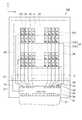
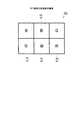
サブ画素SGの配列構造を、図3(a)に示す。サブ画素SGは、マトリクス状に配置されている。そして、8つのサブ画素SGが、略正方形の表示画素AGを構成する。この表示画素AG自体も、さらにマトリクス状に繰り返して配置されている。換言すれば、サブ画素SGは、表示画素AGを繰り返しの最小単位として規則的に配列されている。 An arrangement structure of the sub-pixels SG is shown in FIG. The subpixels SG are arranged in a matrix. The eight subpixels SG constitute a substantially square display pixel AG. The display pixels AG are also repeatedly arranged in a matrix. In other words, the sub-pixels SG are regularly arranged with the display pixel AG as a minimum repeating unit.
各表示画素AGは、2行×4列のサブ画素SGから構成されている。サブ画素SGは、どの表示画素AGにおいても、第1行はRGBW、第2行はBWRGの順にそれぞれ配列されている。また、各表示画素AGにはRGBWのサブ画素SGがそれぞれ2つずつ組み入れられていることから、各表示画素AGにおいては、RGBWの各サブ画素SGの面積は互いに等しくなっている。換言すれば、各表示画素AG内におけるRGBWの各サブ画素SGの面積比は、1:1:1:1である。 Each display pixel AG is composed of 2 × 4 sub-pixels SG. In any display pixel AG, the sub-pixels SG are arranged in the order of RGBW in the first row and BWRG in the second row. Since each display pixel AG incorporates two RGBW sub-pixels SG, the area of each RGBW sub-pixel SG is equal to each other in each display pixel AG. In other words, the area ratio of the RGBW sub-pixels SG in each display pixel AG is 1: 1: 1: 1.
ここで、液晶表示装置100における表示画素AGは、サブ画素SGの配列についての繰り返しの最小単位といった意味をもつものであって、表示の最小単位を意味するものではない。 Here, the display pixel AG in the liquid
液晶表示装置100の画素領域AGは、R、G、B、Wで構成されており、従来よく用いられているR、G、Bで1つの表示画素を構成するものとは異なっている。これにともなって、液晶表示装置100は、従来とは異なる描画操作技術(レンダリング)を用いて表示を行っている。レンダリングは、任意の1表示画素AGにおいてRGB各色の色相をそれぞれ備えたサブ画素SGに印加される階調信号を、当該表示画素AG内のサブ画素のみならず、その表示画素AGの周辺に配置された同一色相のサブ画素SGにも重畳させて印加するという画像処理技術を用いるものである。つまり、1つの表示画素AGにおけるRGBの各色のサブ画素SGは、1つの表示画素AGの周辺の表示画素AGにおける同一色相のサブ画素SGにも、1つの表示画素AG内のサブ画素SGの表示に寄与する階調信号を重畳して印加することにより表示を行うものである。これにより、実際の画素数よりも高い解像度感を視認でき、例えば、QVGA(Quarter Video Graphics Array)規格に対応する画面表示解像度を有する液晶表示装置を用いた場合に、VGA(Video Graphics Array)規格に対応する画面表示解像度を実現する。 The pixel area AG of the liquid
図2に戻り、素子基板91は、カラーフィルタ基板92の一辺側から外側へ張り出してなる張り出し領域31を有しており、その張り出し領域31上には、ドライバIC40、外部接続用配線35及びFPC(Flexible Printed Circuit)41などが形成若しくは実装されている。ドライバIC40の入力側の端子(不図示)は、複数の外部接続用配線35の一端側と電気的に接続されていると共に、複数の外部接続用配線35の他端側はFPC41と電気的に接続されている。各データ線32は、Y方向に延在するようにかつX方向に適宜の間隔をおいて形成されており、各データ線32の一端側は、ドライバIC40の出力側の端子(不図示)に電気的に接続されている。 Returning to FIG. 2, the
各走査線33は、Y方向に延在するように形成された第1配線33aと、その第1配線33aの終端部からX方向に延在するように形成された第2配線33bとを備えている。各走査線33の第2配線33bは、各データ線32と交差する方向、即ちX方向に延在するようにかつY方向に適宜の間隔をおいて形成されており、各走査線33の第1配線33aの一端側は、ドライバIC40の出力側の端子(不図示)に電気的に接続されている。各データ線32と各走査線33の第2配線33bの交差に対応する位置にはTFT素子21が設けられており、TFT素子21は、データ線32、走査線33及び画素電極10等に電気的に接続されている。TFT素子21及び画素電極10は、各サブ画素SGに対応する位置に設けられている。画素電極10は、例えばITO(Indium-Tin Oxide)などの透明導電材料により形成されている。 Each
画素領域AGがX方向及びY方向に複数個、マトリクス状に並べられた領域が画素表示領域20(2点鎖線により囲まれる領域)である。この画素表示領域20に、文字、数字、図形等の画像が表示される。なお、画素表示領域20の外側の領域は表示に寄与しない額縁領域38となっている。また、各データ線32、各走査線33、各TFT素子21、及び各画素電極10等の内面上には、図示しない配向膜が形成されている。 A region in which a plurality of pixel regions AG are arranged in a matrix in the X and Y directions is a pixel display region 20 (a region surrounded by a two-dot chain line). In the
一方、カラーフィルタ基板92の内面上には、共通電極8が形成されている(図1および図5参照)。共通電極8は、画素電極10と同様にITOなどの透明導電材料からなり、カラーフィルタ基板92の略一面にわたって形成されている。共通電極8は、シール部材3の隅の領域E1において配線15の一端側と電気的に接続されていると共に、当該配線15の他端側は、ドライバIC40のCOMに対応する出力端子と電気的に接続されている。 On the other hand, the
以上の構成を有する液晶表示装置100では、電子機器等と接続されたFPC41側からの信号及び電力等に基づき、ドライバIC40によって、G1,G2,…,Gm−1,Gm(mは自然数)の順に走査線33が順次排他的に1本ずつ選択されるとともに、選択された走査線33には、選択電圧のゲート信号が供給される一方、他の非選択の走査線33には、非選択電圧のゲート信号が供給される。そして、ドライバIC40は、選択された走査線33に対応する位置にある画素電極10に対し、表示内容に応じたソース信号を、それぞれ対応するS1,S2,…,Sn−1,Sn(nは自然数)のデータ線32及びTFT素子21を介して供給する。その結果、液晶層4の配向状態が制御されることとなる。 In the liquid
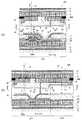
次に、図3(b)等を参照して、1つの画素領域AGの構成について説明する。図3(b)は、図2または図3(a)における1つの画素領域AG(破線によって囲まれた部分)に対応する部分拡大平面図である。図3(b)に示すように、1つの画素領域AGは、R、G、B、Wに対応する、2行×4列のサブ画素SGを備えて構成される。さらに、R、G、B、Wに対応する各サブ画素SGは、透過型表示が行われる透過領域E10と、反射型表示が行われる反射領域E11とを備えて構成される。 Next, the configuration of one pixel area AG will be described with reference to FIG. FIG. 3B is a partially enlarged plan view corresponding to one pixel region AG (portion surrounded by a broken line) in FIG. 2 or FIG. As shown in FIG. 3B, one pixel region AG is configured to include 2 × 4 subpixels SG corresponding to R, G, B, and W. Furthermore, each sub-pixel SG corresponding to R, G, B, and W is configured to include a transmissive region E10 where transmissive display is performed and a reflective region E11 where reflective display is performed.
次に、図4を参照して、図3(b)におけるR、G、B、Wに対応する各サブ画素SGの構成を、反射領域E11の構成と透過領域E10の構成とに分けて説明する。図4(a)は、R、G、B、Wの各サブ画素SGに対応する素子基板91の構成を示す部分拡大平面図である。一方、図4(b)は、図4(a)の素子基板91と対向配置される、R、G、B、Wの各サブ画素SGに対応するカラーフィルタ基板92の構成を示す部分拡大平面図である。図5(a)は、図4(a)及び(b)における切断線A−A’に沿った部分断面図であり、R、G、B、Wの各反射領域E11に対応する液晶表示装置100の断面構成を示す。一方、図5(b)は、図4(a)及び(b)における切断線B−B’に沿った部分断面図であり、R、G、B、Wの各サブ画素SGに対応する液晶表示装置100の断面構成を示す。 Next, with reference to FIG. 4, the configuration of each subpixel SG corresponding to R, G, B, and W in FIG. 3B is divided into the configuration of the reflective region E11 and the configuration of the transmissive region E10. To do. FIG. 4A is a partially enlarged plan view showing the configuration of the
まず、R、G、B、Wの1つのサブ画素SG内における反射領域E11の構成について説明する。図4(a)に示すように、走査線33(図2参照)の第2配線33bは、X方向に延在する本線部分33baと、その本線部分33baからY方向に折れ曲がるように分岐する支線部分33bbとを有する。これらを含む走査線33は、下側基板1上に配置されており、図5(a)においては、その支線部分33bbが描かれている。下側基板1及び走査線33上には、絶縁性を有するゲート絶縁層50が形成されている。ゲート絶縁層50上であって、かつ、走査線33の支線部分33bbと平面的に重なる位置には、TFT素子21の要素であるa−Si層52が設けられている。データ線32は、ゲート絶縁層50上において、走査線33と交差する方向に延在するように形成されている。 First, the configuration of the reflection region E11 in one R, G, B, and W subpixel SG will be described. As shown in FIG. 4A, the
データ線32は、図4(a)に示すように、Y方向に延在する本線部分32aと、その本線部分32aからX方向に折れ曲がるように分岐する支線部分32bとを有する。データ線32の支線部分32bの一部分は、a−Si層52の一端側の一部分上に形成されている。a−Si層52の他端側の一部分上、及び、ゲート絶縁層50上には、金属などよりなる保持容量電極16が形成されている。このため、a−Si層52は、データ線32及び保持容量電極16に夫々電気的に接続されている。そして、a−Si層52に対応する位置には、その層を要素として含むTFT素子21が形成されている。 As shown in FIG. 4A, the
データ線32、保持容量電極16及びゲート絶縁層50等の上には、絶縁性を有するパシベーション層(反応防止層)51が形成されている。パシベーション層51は、保持容量電極16と平面的に重なる位置にコンタクトホール(開口)51aを有する。パシベーション層51上には、樹脂材料などよりなる樹脂層17が形成されている。樹脂層17の表面上には、光を散乱させる機能を有する微小な凹凸が複数形成されている。樹脂層17は、パシベーション層51のコンタクトホール51aに対応する位置にコンタクトホール17aを有する。樹脂層17上には、Al(アルミニウム)などにより形成され反射機能を有する反射電極5が形成されている。反射電極5は、微小な凹凸を複数有する樹脂層17上に形成されているため、その微小な複数の凹凸を反映した形状に形成されている。コンタクトホール51a及び17aに対応する反射電極5の位置には、光を透過させる透過開口領域25が形成されている。反射電極5上および透過開口領域25には、画素電極10が形成されている。 An insulating passivation layer (reaction prevention layer) 51 is formed on the
一方、R、G、Bの1つのサブ画素SG内における反射領域E11に対応するカラーフィルタ基板92の構成は次の通りである。 On the other hand, the configuration of the
下側基板1と同一の材料によりなる上側基板2上であって、かつ、反射領域E11に対応する位置には、R、G、Bの着色層6が形成されている。各着色層6の厚さはd3に設定されている。着色層6は、透過領域E10と反射領域E11とで均一な色を表示させる機能を有する開口6aを有する。相隣接する着色層6を区画する位置には、黒色遮光層BMが形成されている。着色層6上には、樹脂材料などよりなるオーバーコート層18が形成されている。オーバーコート層18の厚さはd4に設定される。オーバーコート層18の厚さd4をサブ画素SGごとに調整することによって、R、G、B、Wの各反射領域E11に対応する液晶層4の厚さ(セル厚)d2を、サブ画素SGごとに変えることができる。オーバーコート層18等の上には、共通電極8が形成されている。 R, G, and B colored layers 6 are formed on the
以上に述べた反射領域E11に対応する素子基板91と、当該反射領域E11に対応するカラーフィルタ基板92とは液晶層4を介して対向している。そして、反射領域E11に対応する液晶層4の厚さは、上記したようにd2に設定されている。 The
次に、R、G、B、Wの1つのサブ画素領域SG内における透過領域E10の構成について説明する。 Next, the configuration of the transmissive region E10 in one sub-pixel region SG of R, G, B, and W will be described.
下側基板1上には、図5(b)に示すように、ゲート絶縁層50が形成されている。ゲート絶縁層50上には、パシベーション層51が形成されている。パシベーション層51上には、樹脂層17が形成されている。上記したように、反射領域E11に形成された樹脂層17は、その表面上に微小な凹凸が形成されているのに対し、透過領域E10に形成された樹脂層17は、その表面上に微小な凹凸は形成されていない。即ち、透過領域E10に形成された樹脂層17の表面は略平坦性を有するように形成されている。樹脂層17上には、画素電極10が形成されている。 On the
一方、R、G、B、Wの1つのサブ画素領域SG内における透過領域E10に対応するカラーフィルタ基板92の構成は次の通りである。上側基板2上には、着色層6が形成されている。その各着色層6上には、厚さd5のオーバーコート層18が形成されている。オーバーコート層18は、厚さd5を調整することによって、R、G、B、Wの各透過領域E10に対応する液晶層4の厚さ(セルの厚さ)d1をサブ画素SGごとに変えることができる。オーバーコート層18上には、共通電極8が形成されている。また、上側基板2の外面上には位相差板11が配置されていると共に、位相差板11の外面上には偏光板12が配置されている。 On the other hand, the configuration of the
以上に述べた透過領域E10に対応する素子基板91と、当該透過領域E10に対応するカラーフィルタ基板92とは液晶層4を介して対向している。また、各サブ画素SGにおいて、透過領域E10のオーバーコート層18の厚さd5と、反射領域E11のオーバーコート層18の厚さd4とが異なるように設定されている。これにより、透過領域E10の液晶層4の厚さd1は、反射領域E11の液晶層4の厚さd2より大きくなっており、いわゆるマルチギャップ構造をなしている。 The
これに加えて、透過領域E10の液晶層4の厚さd1は、図1の説明において述べたように、R、G、B、Wのサブ画素SGにおいてそれぞれdr、dg、db、dwの値をとる。また、反射領域E11の液晶層4の厚さd2も、厚さd1と同様にしてサブ画素SGごとに値が設定される。したがって、液晶層4のセル厚は、最大で8つの異なる値をとることとなる。厚さd2をサブ画素ごとに異ならせる趣旨は、厚さd1についての趣旨と同様であるので、本稿では厚さd1(dr、dg、db、dw)に関連する事項についてのみ説明する。 In addition, as described in the description of FIG. 1, the thickness d1 of the
(セル厚の大きさと透過率の関係)
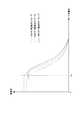
次にセル厚の大きさと透過率の関係について述べる。図6は、一般的な液晶表示装置における、各色のサブ画素での印加電圧と透過率の関係を示すグラフである。この一般的な液晶表示装置は、RGBの各色のサブ画素より構成され、ノーマリーホワイトの液晶表示装置である。また、この一般的な液晶表示装置において、RGBの各色のサブ画素におけるセル厚は、すべて同じ一定の厚さとされている。ここで、横軸は、サブ画素における画素電極10と共通電極8の間に印加される印加電圧の大きさを示し、縦軸は、RGBの各色のサブ画素における光の透過率を示している。ここで、RGBのサブ画素の光の透過率は、液晶層4の液晶の配向状態によって決まる。(Relationship between cell thickness and transmittance)
Next, the relationship between the cell thickness and the transmittance will be described. FIG. 6 is a graph showing the relationship between the applied voltage and the transmittance in each color sub-pixel in a general liquid crystal display device. This general liquid crystal display device is a normally white liquid crystal display device composed of RGB sub-pixels. In this general liquid crystal display device, the cell thicknesses of the sub-pixels for each color of RGB are all the same and constant. Here, the horizontal axis indicates the magnitude of the applied voltage applied between the
図6において、印加電圧を上げていくと、ある一定の電圧Vcまでは、Rのサブ画素、Gのサブ画素、Bのサブ画素のそれぞれにおける光の透過率に変化はない。しかしながら、印加電圧が電圧Vcよりも大きくなる場合、即ち中間調表示の場合、液晶層4の液晶の配向状態が変化し、Rのサブ画素、Gのサブ画素、Bのサブ画素のそれぞれにおける光の透過率もそれに伴い変化する。印加電圧が電圧Vcよりも大きくなる場合、各色のサブ画素における光の透過率を示す曲線(以下、単に「VTカーブ」と称す)は急激に下がる特性を示す。即ち、各色のサブ画素における光の透過率は低下する。各色のサブ画素におけるVTカーブの下がり方の特性は、各色のサブ画素ごとに異なり、Rのサブ画素における透過率の低下が最も大きく、Bのサブ画素における透過率の低下が最も小さい。従って、印加電圧が電圧Vcよりも大きくなる場合、各色のサブ画素の透過率は、高い順に、Bのサブ画素、Gのサブ画素、Rのサブ画素の順となる。従って、一般的な液晶表示装置では、上記のように各サブ画素のセル厚が等しい場合には、同じ階調の中間調表示において全画素の表示を行うと常に青みがかった白色表示となる。 In FIG. 6, when the applied voltage is increased, the light transmittance in each of the R subpixel, the G subpixel, and the B subpixel does not change until a certain voltage Vc is reached. However, when the applied voltage is higher than the voltage Vc, that is, in the case of halftone display, the alignment state of the liquid crystal in the
なお、横軸を、反射電極5と共通電極8の間に印加される印加電圧の大きさとし、縦軸をサブ画素の光の反射率としても、サブ画素の光の反射率は、液晶層4の液晶の配向状態によって決まる値なので、図6と同様の特性を示すグラフとなる。従って、この場合においても、印加電圧が電圧Vcよりも大きくなる場合における各色のサブ画素の透過率は、高い順に、Bのサブ画素、Gのサブ画素、Rのサブ画素の順となる。従って、このときも、各サブ画素のセル厚が等しい場合には、同じ階調の中間調表示において全画素の表示を行う場合、常に青みがかった白色表示となる。 The horizontal axis represents the magnitude of the applied voltage applied between the
そこで、このような色づきを抑えるために、本実施形態に係る液晶表示装置100では、液晶層4の複屈折率Δnとセル厚の厚さdの積で規定されるリタデーション値Δn・dを、R≧G≧Bとなるように設定する。具体的には、Rの光の波長をλr(650nm程度)、Gの光の波長をλg(550nm程度)、Bの光の波長をλb(400nm程度)、λr、λg、λbにおける液晶層4の複屈折率をそれぞれΔnr、Δng、Δnbとし、R、G、Bそれぞれのサブ画素SGのセル厚をdr、dg、dbとすると、R、G、Bそれぞれのサブ画素SGにおけるリタデーション値と光の波長との比Δnr・dr/λr、Δng・dg/λg、Δnb・db/λbは、それぞれ同じ大きさの値に設定される。ここで、液晶層4の複屈折率Δnは、通過する光の波長によって異なるが、ほぼ一定である。従って、各色のサブ画素SGにおけるセル厚は、dr≧dg≧db(但し、dr=dg=dbとなることはない)の関係が成立する。なお、各色のサブ画素SGのリタデーション値の範囲としては、360nm≦R(=Δnr・dr)≦700nm、340nm≦G(=Δng・dg)≦600nm、340nm≦B(=Δnb・db)≦500nmとなる。 Therefore, in order to suppress such coloring, in the liquid
このようにRGBの各色のサブ画素SGのセル厚を設定することで、各色のサブ画素SGを出光する光は、液晶層4を通過するとき、干渉により強め合わされる。これにより、本実施形態に係る液晶表示装置100では、図6に示した各色のサブ画素SGのVTカーブを一致させることができ、サブ画素SGに印加される印加電圧の大きさが、電圧Vc以上となる値であっても、白色表示の際の色づきを抑えることができる。 Thus, by setting the cell thickness of the subpixel SG for each color of RGB, the light emitted from the subpixel SG for each color is intensified by interference when passing through the
本実施形態に係る液晶表示装置100では、さらにWのサブ画素SGを有する。Wのサブ画素SGにおけるリタデーション値Δnw・dwは、Rの光の波長λrとBの光の波長λbの間に設定される。即ち、Wのサブ画素SGにおけるセル厚dwは、dr≧dw≧db(但し、dr=dw=dbとなることはない)の関係が成立する値に設定される。Wのサブ画素SGにおけるリタデーション値Δnw・dwを、Rの光の波長λrに近い値に設定すれば、白色表示時において、Wのサブ画素SGにおけるRの光の透過効率が高まり、赤みがかった白色表示となる。同様に、Bの光の波長λbに近い値に設定すれば、白色表示時において、Wのサブ画素SGにおけるBの光の透過効率が高まり、青みがかった白色表示となる。このように、Wのサブ画素SGにおけるリタデーション値Δnw・dwを調整することで、即ち、セル厚dwを調整することで、ホワイトバランスを所定の色温度の状態に設定することができ、ユーザにとって所望の白色表示を実現することができる。 The liquid
(ホワイトバランスの調整の応用例)
本実施形態の液晶表示装置100は、図3(a)に示すように、表示画素AGにおけるR、G、B、Wのサブ画素SGの面積がすべて等しい。このような場合には、R、G、Bの3色のサブ画素SGの面積比に起因したホワイトバランスのずれは生じない。このため、Wのサブ画素SGにおけるリタデーション値Δnw・dwの調整においては、λrに近づけて赤みがかった白表示としたり、λbに近づけて青みがかった白表示としたりする必要はない。したがって、Wのサブ画素SGのセル厚dwは、視感度が最も高く輝度を確保しやすいGの波長に近い値、即ち、dr≧dw≒dg≧db(但し、dr=dw=dbとなることはない)となる値に設定する。もしくは、Wのサブ画素SGにおけるリタデーション値Δnw・dwは、Gのサブ画素SGにおけるリタデーション値Δng・dgと等しくなるように設定する。このような構成によれば、輝度の高い表示を行うことができる。(Application example of white balance adjustment)
In the liquid
下表1は、液晶表示装置100において、Gのサブ画素SGのセル厚dgを3.0μmで一定とした場合に、Wのサブ画素SGのセル厚dwを2.6μmまたは3.0μmとしたときの輝度を比較したものである。この表より、セル厚dwをセル厚dgと等しくする(すなわち3.0μmとする)ことによって、表示の輝度が高まることがわかる。 Table 1 below shows that in the liquid

<第2の実施形態>
続いて、本発明の第2の実施形態に係る液晶表示装置200について説明する。液晶表示装置200は、各表示画素AGにおけるサブ画素SGの配列構造が第1の実施形態の液晶表示装置100と異なるものである。その他の構成については液晶表示装置100と同様であるので、以下の説明に用いる各図においては、液晶表示装置100と同一の構成要素には同一の符号を付すことにして説明は省略する。<Second Embodiment>
Subsequently, a liquid
(液晶表示装置の構成)
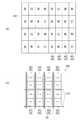
図7は、本実施形態に係る液晶表示装置200の概略構成を模式的に示す平面図である。液晶表示装置200は、各表示画素AGが2行×3列の6つのサブ画素SGからなる点で液晶表示装置100と異なる。(Configuration of liquid crystal display device)
FIG. 7 is a plan view schematically showing a schematic configuration of the liquid
液晶表示装置200における表示画素AG内のサブ画素SGの配列構造を、図8に示す。表示画素AGは、2行3列のサブ画素SGを有し、2つのRのサブ画素SG、2つのGのサブ画素SG、1つのBのサブ画素SG、1つのW(非着色又は白色)のサブ画素SGの6つのサブ画素SGより構成される。より詳しくは、第1行はRBG、第2行はGWRの順にそれぞれ配列されている。液晶表示装置200の画素表示領域20(図7参照)には、こうした表示画素AGがマトリクス状に繰り返し配列されている。ここで、液晶表示装置200における表示画素AGは、サブ画素SGの配列についての繰り返しの最小単位といった意味をもつものであって、表示の最小単位を意味するものではない。液晶表示装置200は、液晶表示装置100と同様に、レンダリングを用いて表示を行う。 An arrangement structure of the sub-pixels SG in the display pixel AG in the liquid
ここで、Bのサブ画素SGの数がRやGのサブ画素SGの数に比較して少ない理由は、Bのサブ画素SGはGやRと比較して輝度情報をあまり担っておらず、色のバランスをとっているに過ぎないため、Wのサブ画素SGに代えることで格段に輝度を向上することができるからである。このように、表示画素AGの画素配列構造では、RGBの各サブ画素SGを液晶表示装置上で均等に配置するのではなく、RGBそれぞれのサブ画素SGの面積および配置を、人間の色に対する視覚特性を考慮して最適化されている。そのため、図8に示す表示画素AGを有する液晶表示装置200では、一般的な液晶表示装置に比べて少ないサブ画素数で人間の視覚にとって高画質の表示を実現することができる。 Here, the reason why the number of B sub-pixels SG is smaller than the number of R or G sub-pixels SG is that the B sub-pixel SG does not bear much luminance information as compared with G or R. This is because the color balance is merely achieved, and the luminance can be significantly improved by replacing the subpixel SG with W. As described above, in the pixel array structure of the display pixels AG, the RGB sub-pixels SG are not evenly arranged on the liquid crystal display device, but the areas and arrangements of the RGB sub-pixels SG are visually recognized with respect to human colors. Optimized considering characteristics. Therefore, the liquid
(ホワイトバランスの調整の応用例)
図8に示す表示画素AGでは、Bのサブ画素SGの数が、RやGのサブ画素SGの数に比較して少ないので、表示画素AG全体から見ると、Bのサブ画素SGの面積は、RやGのサブ画素SGの面積に比較して小さくなる。具体的には、表示画素AGは、RGBのサブ画素SGのうちのBのサブ画素SGとWのサブ画素SGの合計面積が、他の2色のサブ画素SGの各々の面積と略等しく構成されている。図8に示す表示画素AGでは、一例として、表示画素AGは、前記RGB及び非着色の各色のサブ画素SGの面積の比率が2:2:1:1とされている。このような画素配列構造の表示画素AGを有する液晶表示装置200において、白色表示を行う場合、Bの色の光が不足するので、黄色みがかった白色表示となる。本実施形態に係る液晶表示装置200では、このような白色表示における色付きを抑えるために、Wのサブ画素SGにおけるリタデーション値Δnw・dwをBのサブ画素SGにおけるリタデーション値Δnb・dbに近い値に設定することとする。つまり、Wのサブ画素SGにおけるセル厚を調整して、Bのセル厚とほぼ等しく設定する。これにより、Wのサブ画素SGより出光する光は、Bの色の成分が強調され、不足しているBの色の光を補うことができ、Bのサブ画素SGの面積が小さいことによって発生する白色表示における上述した色付きを抑えることができる。このようにすることで、Wのサブ画素SGにおけるセル厚を調整して、Bの光の成分を強調することにより、表示画素AGにおけるBの色の光を補うことができ、白色表示の色付きを抑えることができる。(Application example of white balance adjustment)
In the display pixel AG shown in FIG. 8, since the number of B subpixels SG is smaller than the number of R and G subpixels SG, the area of the B subpixel SG is as viewed from the entire display pixel AG. , R and G are smaller than the area of the subpixel SG. Specifically, the display pixel AG is configured such that the total area of the B subpixel SG and the W subpixel SG among the RGB subpixels SG is substantially equal to the area of each of the other two subpixels SG. Has been. In the display pixel AG shown in FIG. 8, as an example, the display pixel AG has an area ratio of 2: 2: 1: 1 for the RGB and non-colored sub-pixels SG. In the liquid
下表2は、液晶表示装置200において、Bのサブ画素SGのセル厚dbを2.6μmで一定とした場合に、Wのサブ画素SGのセル厚dwを3.0μmまたは2.6μmとしたときの白表示の色度座標を示したものである。また、図9は、表2の色度座標をx−y座標上にプロットしたものである。これらの表および図から、セル厚dwをセル厚dbと等しく(2.6μmに)することによって、白表示の色座標が白点に近付くことがわかる(図9中の破線の矢印)。 Table 2 below shows that in the liquid
上述した応用例では、Bのサブ画素SGの面積が、他の色のサブ画素SGに比較して小さい場合について述べたが、Bのサブ画素SGに限らず、他の色のサブ画素SGの面積が小さい場合にも、本発明の手法を用いることができるのは言うまでもない。このとき、表示画素AGは、RGBのサブ画素SGのうちの1色のサブ画素SGとWのサブ画素SGの合計面積が、他の2色のサブ画素SGの各々の面積と略等しく構成されている。この場合、Wのサブ画素SGのセル厚を調整して、Wのサブ画素SGのセル厚を、表示画素AGでのサブ画素SGの面積が最も小さい色のセル厚にほぼ等しくなるように設定する。このようにすることで、Wのサブ画素SGから出光される光は、表示画素AGでのサブ画素SGの面積が最も小さい色の光の成分を強調して出光することができ、表示画素AGにおけるその色の光の不足分を補うことができる。このように、Wのサブ画素SGのセル厚を、サブ画素SGの面積が最も小さい色のセル厚とほぼ等しく設定することにより、白色表示におけるホワイトバランスを所定の色温度の状態に設定することができ、白色表示における色付きを抑えることができる。 In the application example described above, the case where the area of the B sub-pixel SG is smaller than the sub-pixel SG of the other color has been described. However, the sub-pixel SG of the other color is not limited to the sub-pixel SG of the other color. Needless to say, the method of the present invention can be used even when the area is small. At this time, the display pixel AG is configured so that the total area of one color subpixel SG and the W subpixel SG among the RGB subpixels SG is substantially equal to the area of each of the other two color subpixels SG. ing. In this case, the cell thickness of the W sub-pixel SG is adjusted so that the cell thickness of the W sub-pixel SG is approximately equal to the cell thickness of the color with the smallest area of the sub-pixel SG in the display pixel AG. To do. In this way, the light emitted from the W sub-pixel SG can be emitted while emphasizing the light component of the color having the smallest area of the sub-pixel SG in the display pixel AG. Can compensate for the lack of light of that color. In this way, by setting the cell thickness of the W sub-pixel SG to be substantially equal to the cell thickness of the color having the smallest area of the sub-pixel SG, the white balance in white display is set to a predetermined color temperature state. And coloration in white display can be suppressed.
(電子機器)
次に、本実施形態に係る液晶表示装置100(液晶表示装置200を含む。以下同じ。)を適用可能な電子機器の具体例について図10を参照して説明する。(Electronics)
Next, a specific example of an electronic apparatus to which the liquid
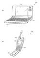
まず、本実施形態に係る液晶表示装置100を、可搬型のパーソナルコンピュータ(いわゆるノート型パソコン)の表示部に適用した例について説明する。図10(a)は、このパーソナルコンピュータの構成を示す斜視図である。同図に示すように、パーソナルコンピュータ710は、キーボード711を備えた本体部712と、本発明に係る液晶表示装置100を適用した表示部713とを備えている。 First, an example in which the liquid
続いて、本実施形態に係る液晶表示装置100を、携帯電話機の表示部に適用した例について説明する。図10(b)は、この携帯電話機の構成を示す斜視図である。同図に示すように、携帯電話機720は、複数の操作ボタン721のほか、受話口722、送話口723とともに、本実施形態に係る液晶表示装置100を適用した表示部724を備える。 Next, an example in which the liquid
なお、本実施形態に係る液晶表示装置100を適用可能な電子機器としては、図10(a)に示したパーソナルコンピュータや図10(b)に示した携帯電話機の他にも、液晶テレビ、ビューファインダ型・モニタ直視型のビデオテープレコーダ、カーナビゲーション装置、ページャ、電子手帳、電卓、ワードプロセッサ、ワークステーション、テレビ電話、POS端末、ディジタルスチルカメラなどが挙げられる。 Electronic devices to which the liquid
1…下側基板、2…上側基板、4…液晶層、5…反射電極、6…着色層、8…共通電極、10…画素電極、18…オーバーコート層、21…TFT素子、91…素子基板、92…カラーフィルタ基板、AG…表示画素、SG…サブ画素、BM…黒色遮光層、100,200…液晶表示装置、710…電子機器としてのパーソナルコンピュータ、720…電子機器としての携帯電話機。
DESCRIPTION OF
Claims (2)
Translated fromJapaneseRGB及び非着色の4つのサブ画素を有して構成され、前記RGB及び非着色の各サブ画素の面積の比率が2:2:1:1となる構成を有する表示画素と、
前記一対の基板の間に挟持される液晶層と、を備え、
前記RGB及び非着色の4つのサブ画素で、前記液晶層のセル厚を調整することによって、
前記R、G、B、非着色の各サブ画素は、夫々のセル厚の大きさをdr、dg、db、dwとすると、dr≧dg≧dw≒db(但し、dr=dw=dbとなることはない)となる関係を有することを特徴とする液晶表示装置。A pair of substrates;
Display pixels having four sub-pixels of RGB and non-colored, and having a configuration in which the ratio of the areas of the RGB and non-colored sub-pixels is 2: 2: 1: 1;
A liquid crystal layer sandwiched between the pair of substrates,
By adjusting the cell thickness of the liquid crystal layer with the four sub-pixels of RGB and non-colored,
For each of the R, G, B, and non-colored sub-pixels, dr ≧ dg ≧ dw≈db (provided that dr = dw = db) when the cell thicknesses are dr, dg, db, and dw. A liquid crystal display device characterized by having a relationship of
Priority Applications (3)
| Application Number | Priority Date | Filing Date | Title |
|---|---|---|---|
| JP2006163117AJP4501899B2 (en) | 2005-07-06 | 2006-06-13 | Liquid crystal display device and electronic device |
| KR1020060062803AKR100825148B1 (en) | 2005-07-06 | 2006-07-05 | Liquid crystal display and electronics |
| US11/480,836US20070008463A1 (en) | 2005-07-06 | 2006-07-06 | Liquid crystal display device and electronic apparatus |
Applications Claiming Priority (2)
| Application Number | Priority Date | Filing Date | Title |
|---|---|---|---|
| JP2005197073 | 2005-07-06 | ||
| JP2006163117AJP4501899B2 (en) | 2005-07-06 | 2006-06-13 | Liquid crystal display device and electronic device |
Publications (2)
| Publication Number | Publication Date |
|---|---|
| JP2007041551A JP2007041551A (en) | 2007-02-15 |
| JP4501899B2true JP4501899B2 (en) | 2010-07-14 |
Family
ID=37617999
Family Applications (1)
| Application Number | Title | Priority Date | Filing Date |
|---|---|---|---|
| JP2006163117AActiveJP4501899B2 (en) | 2005-07-06 | 2006-06-13 | Liquid crystal display device and electronic device |
Country Status (3)
| Country | Link |
|---|---|
| US (1) | US20070008463A1 (en) |
| JP (1) | JP4501899B2 (en) |
| KR (1) | KR100825148B1 (en) |
Families Citing this family (8)
| Publication number | Priority date | Publication date | Assignee | Title |
|---|---|---|---|---|
| JP5032157B2 (en)* | 2007-03-05 | 2012-09-26 | 株式会社ジャパンディスプレイセントラル | Liquid crystal display |
| JP2010169704A (en)* | 2009-01-20 | 2010-08-05 | Casio Computer Co Ltd | Liquid crystal display apparatus |
| JP4877363B2 (en) | 2009-06-29 | 2012-02-15 | カシオ計算機株式会社 | Liquid crystal display device and driving method thereof |
| CN102725681B (en)* | 2010-01-29 | 2015-01-28 | 夏普株式会社 | Liquid crystal display device |
| JP6098196B2 (en)* | 2013-02-05 | 2017-03-22 | セイコーエプソン株式会社 | Electro-optical device and electronic apparatus |
| JP2015025835A (en)* | 2013-07-24 | 2015-02-05 | セイコーエプソン株式会社 | Color filter substrate, electro-optic device, projection type display device, and manufacturing method of color filter substrate |
| US10388705B2 (en)* | 2014-05-27 | 2019-08-20 | Lg Display Co., Ltd. | Display panel and method for manufacturing thereof |
| CN105404052A (en)* | 2016-01-05 | 2016-03-16 | 京东方科技集团股份有限公司 | Curved-surface display panel |
Family Cites Families (59)
| Publication number | Priority date | Publication date | Assignee | Title |
|---|---|---|---|---|
| DE3650639T2 (en)* | 1985-01-25 | 1998-02-26 | Nippon Electric Co | Construction of a liquid crystal multicolor display panel |
| JP3029489B2 (en)* | 1991-07-25 | 2000-04-04 | キヤノン株式会社 | Display device |
| JPH07128640A (en)* | 1993-10-29 | 1995-05-19 | Sharp Corp | Ferroelectric liquid crystal display device |
| US5673127A (en)* | 1993-12-01 | 1997-09-30 | Matsushita Electric Industrial Co., Ltd. | Display panel and display device using a display panel |
| KR0156765B1 (en)* | 1993-12-27 | 1998-11-16 | 사토 후미오 | Display device |
| US7123216B1 (en)* | 1994-05-05 | 2006-10-17 | Idc, Llc | Photonic MEMS and structures |
| US7138984B1 (en)* | 2001-06-05 | 2006-11-21 | Idc, Llc | Directly laminated touch sensitive screen |
| US6573961B2 (en)* | 1994-06-27 | 2003-06-03 | Reveo, Inc. | High-brightness color liquid crystal display panel employing light recycling therein |
| US5936693A (en)* | 1994-09-27 | 1999-08-10 | Casio Computer Co., Ltd. | Liquid crystal display device having a wide view angle |
| US6560018B1 (en)* | 1994-10-27 | 2003-05-06 | Massachusetts Institute Of Technology | Illumination system for transmissive light valve displays |
| JPH08294137A (en)* | 1995-04-20 | 1996-11-05 | Mitsubishi Electric Corp | Projector device |
| US7289174B1 (en)* | 1995-07-17 | 2007-10-30 | Seiko Epson Corporation | Reflective type color liquid crystal device and an electronic apparatus using this |
| EP1598693A3 (en)* | 1995-07-17 | 2005-11-30 | Seiko Epson Corporation | Reflective mode colour liquid crystal display having enhanced luminosity |
| JPH09197445A (en)* | 1996-01-16 | 1997-07-31 | Fujitsu Ltd | Color liquid crystal panel |
| US6072555A (en)* | 1996-02-01 | 2000-06-06 | Canon Kabushiki Kaisha | Display apparatus capable of gradational display |
| US5899550A (en)* | 1996-08-26 | 1999-05-04 | Canon Kabushiki Kaisha | Display device having different arrangements of larger and smaller sub-color pixels |
| US6016178A (en)* | 1996-09-13 | 2000-01-18 | Sony Corporation | Reflective guest-host liquid-crystal display device |
| JPH10170905A (en)* | 1996-12-09 | 1998-06-26 | Alps Electric Co Ltd | Color polarization filter for reflection and reflection-type color liquid crystal display device using the filter |
| US6124909A (en)* | 1996-12-25 | 2000-09-26 | Casio Computer Co., Ltd. | Color liquid crystal display device having a plurality of pixel areas which emit non-colored light |
| US6195140B1 (en)* | 1997-07-28 | 2001-02-27 | Sharp Kabushiki Kaisha | Liquid crystal display in which at least one pixel includes both a transmissive region and a reflective region |
| US6215538B1 (en)* | 1998-01-26 | 2001-04-10 | Sharp Kabushiki Kaisha | Liquid crystal display including both color filter and non-color filter regions for increasing brightness |
| JP3368823B2 (en)* | 1998-04-15 | 2003-01-20 | カシオ計算機株式会社 | Liquid crystal display device |
| JP3448871B2 (en)* | 1998-10-07 | 2003-09-22 | セイコーエプソン株式会社 | Liquid crystal devices and electronic equipment |
| WO2003007049A1 (en)* | 1999-10-05 | 2003-01-23 | Iridigm Display Corporation | Photonic mems and structures |
| US7283142B2 (en)* | 2000-07-28 | 2007-10-16 | Clairvoyante, Inc. | Color display having horizontal sub-pixel arrangements and layouts |
| US7274383B1 (en)* | 2000-07-28 | 2007-09-25 | Clairvoyante, Inc | Arrangement of color pixels for full color imaging devices with simplified addressing |
| EP1331513A4 (en)* | 2000-10-17 | 2008-04-02 | Toshiba Matsushita Display Tec | Liquid crystal display and its producing method |
| US7221381B2 (en)* | 2001-05-09 | 2007-05-22 | Clairvoyante, Inc | Methods and systems for sub-pixel rendering with gamma adjustment |
| US7184066B2 (en)* | 2001-05-09 | 2007-02-27 | Clairvoyante, Inc | Methods and systems for sub-pixel rendering with adaptive filtering |
| US6714206B1 (en)* | 2001-12-10 | 2004-03-30 | Silicon Image | Method and system for spatial-temporal dithering for displays with overlapping pixels |
| KR100870003B1 (en)* | 2001-12-24 | 2008-11-24 | 삼성전자주식회사 | Liquid crystal display |
| US20040051724A1 (en)* | 2002-09-13 | 2004-03-18 | Elliott Candice Hellen Brown | Four color arrangements of emitters for subpixel rendering |
| TWI227340B (en)* | 2002-02-25 | 2005-02-01 | Himax Tech Inc | Color filter and liquid crystal display |
| CN1324363C (en)* | 2002-05-04 | 2007-07-04 | 三星电子株式会社 | Liquid crystal display and its color filter array board |
| JP4200830B2 (en)* | 2002-10-11 | 2008-12-24 | セイコーエプソン株式会社 | Electro-optical device manufacturing method, electro-optical device, and electronic apparatus |
| KR100907479B1 (en)* | 2002-12-31 | 2009-07-13 | 삼성전자주식회사 | Color filter substrate and liquid crystal display having the same |
| KR20040080778A (en)* | 2003-03-13 | 2004-09-20 | 삼성전자주식회사 | Liquid crystal displays using 4 color and panel for the same |
| JP4366988B2 (en)* | 2003-05-01 | 2009-11-18 | セイコーエプソン株式会社 | Organic EL device and electronic device |
| KR100978254B1 (en)* | 2003-06-30 | 2010-08-26 | 엘지디스플레이 주식회사 | 4-pixel structure transverse electric field mode liquid crystal display device |
| KR100563466B1 (en)* | 2003-11-27 | 2006-03-23 | 엘지.필립스 엘시디 주식회사 | Color Filter Array Substrate And Fabricating Method Thereof |
| KR101033461B1 (en)* | 2003-12-23 | 2011-05-11 | 엘지디스플레이 주식회사 | Liquid crystal display device and manufacturing method thereof |
| KR101072375B1 (en)* | 2003-12-29 | 2011-10-11 | 엘지디스플레이 주식회사 | Liquid Crystal Display Device Automatically Adjusting Aperture Ratio In Each Pixel |
| US7248268B2 (en)* | 2004-04-09 | 2007-07-24 | Clairvoyante, Inc | Subpixel rendering filters for high brightness subpixel layouts |
| JP4208763B2 (en)* | 2004-04-28 | 2009-01-14 | キヤノン株式会社 | Color display element and color liquid crystal display element |
| JP4328738B2 (en)* | 2004-05-06 | 2009-09-09 | キヤノン株式会社 | LCD color display |
| JP2005321458A (en)* | 2004-05-06 | 2005-11-17 | Canon Inc | Color liquid crystal display element |
| CN1993448B (en)* | 2004-07-07 | 2010-05-12 | 默克专利股份有限公司 | Biaxial film II |
| KR20070028522A (en)* | 2004-07-07 | 2007-03-12 | 코닌클리케 필립스 일렉트로닉스 엔.브이. | Color display |
| CN1993636B (en)* | 2004-07-07 | 2012-12-05 | 默克专利股份有限公司 | Biaxial film having local birefringence that varies periodically |
| JP4145852B2 (en)* | 2004-08-20 | 2008-09-03 | セイコーエプソン株式会社 | Electro-optical device, color filter, and electronic device |
| US7388635B2 (en)* | 2004-11-26 | 2008-06-17 | Kyocera Corporation | Liquid crystal display device and display equipment using the same |
| US20060132677A1 (en)* | 2004-12-06 | 2006-06-22 | Yasufumi Asao | Color liquid crystal display device and color liquid crystal display apparatus |
| TWI386744B (en)* | 2004-12-14 | 2013-02-21 | Samsung Display Co Ltd | Thin film transistor panel and liquid crystal display using the same |
| US20060139527A1 (en)* | 2004-12-27 | 2006-06-29 | Wei-Chih Chang | Liquid crystal display device with transmission and reflective display modes and method of displaying balanced chromaticity image for the same |
| JP2006276831A (en)* | 2005-03-03 | 2006-10-12 | Sanyo Epson Imaging Devices Corp | Color filter substrate, liquid crystal unit, and electronic device |
| JP4151702B2 (en)* | 2005-07-06 | 2008-09-17 | エプソンイメージングデバイス株式会社 | Liquid crystal device, method for manufacturing the same, and electronic device |
| JP4950480B2 (en)* | 2005-11-22 | 2012-06-13 | 東芝モバイルディスプレイ株式会社 | Liquid crystal display |
| US7382515B2 (en)* | 2006-01-18 | 2008-06-03 | Qualcomm Mems Technologies, Inc. | Silicon-rich silicon nitrides as etch stops in MEMS manufacture |
| JP4927430B2 (en)* | 2006-04-12 | 2012-05-09 | 株式会社 日立ディスプレイズ | Liquid crystal display |
- 2006
- 2006-06-13JPJP2006163117Apatent/JP4501899B2/enactiveActive
- 2006-07-05KRKR1020060062803Apatent/KR100825148B1/enactiveActive
- 2006-07-06USUS11/480,836patent/US20070008463A1/ennot_activeAbandoned
Also Published As
| Publication number | Publication date |
|---|---|
| JP2007041551A (en) | 2007-02-15 |
| KR20070005506A (en) | 2007-01-10 |
| KR100825148B1 (en) | 2008-04-24 |
| US20070008463A1 (en) | 2007-01-11 |
Similar Documents
| Publication | Publication Date | Title |
|---|---|---|
| JP4197000B2 (en) | Electro-optical device and electronic apparatus | |
| JP4717672B2 (en) | Liquid crystal device and electronic device | |
| JP4572854B2 (en) | Liquid crystal device and electronic device | |
| US7688408B2 (en) | Liquid crystal device and electronic apparatus | |
| KR100818005B1 (en) | Electro-optical device and electronic apparatus | |
| JP4501899B2 (en) | Liquid crystal display device and electronic device | |
| JP2006139058A (en) | Liquid crystal display device and electronic device | |
| US20070109453A1 (en) | Electro-optical apparatus and electronic apparatus | |
| CN100476540C (en) | Electro-optical devices and electronic equipment | |
| JP2008139528A (en) | Electro-optical device and electronic appliance | |
| KR100636559B1 (en) | Liquid crystal display device and electronic apparatus | |
| JP2007279197A (en) | Liquid crystal device and electronic equipment | |
| US8736793B2 (en) | Liquid crystal display panel, and liquid crystal display device | |
| JP4211773B2 (en) | Electro-optical device and electronic apparatus | |
| JP2007199513A (en) | Electro-optical apparatus | |
| JP2007094025A (en) | Electrooptic device and electronic equipment | |
| JP2007206585A (en) | Electro-optical device and electronic apparatus | |
| JP2007148205A (en) | Electrooptical device and electronic appliance | |
| JP2007226084A (en) | Display device, color filter, liquid crystal display device provided with them, panel for liquid crystal display device and electronic equipment | |
| JP2007094029A (en) | Electrooptical apparatus and electronic device | |
| JP2007121326A (en) | Electrooptical device and electronic appliance | |
| JP4259502B2 (en) | Liquid crystal display device and electronic device | |
| JP2007140240A (en) | Electrooptical device and electronic equipment | |
| JP2007065602A (en) | Liquid crystal device and electronic apparatus | |
| JP2006145719A (en) | Electro-optical device and electronic apparatus |
Legal Events
| Date | Code | Title | Description |
|---|---|---|---|
| RD04 | Notification of resignation of power of attorney | Free format text:JAPANESE INTERMEDIATE CODE: A7424 Effective date:20070406 | |
| A977 | Report on retrieval | Free format text:JAPANESE INTERMEDIATE CODE: A971007 Effective date:20090622 | |
| A131 | Notification of reasons for refusal | Free format text:JAPANESE INTERMEDIATE CODE: A131 Effective date:20091102 | |
| A521 | Request for written amendment filed | Free format text:JAPANESE INTERMEDIATE CODE: A523 Effective date:20091202 | |
| A131 | Notification of reasons for refusal | Free format text:JAPANESE INTERMEDIATE CODE: A131 Effective date:20100105 | |
| A521 | Request for written amendment filed | Free format text:JAPANESE INTERMEDIATE CODE: A523 Effective date:20100303 | |
| TRDD | Decision of grant or rejection written | ||
| A01 | Written decision to grant a patent or to grant a registration (utility model) | Free format text:JAPANESE INTERMEDIATE CODE: A01 Effective date:20100330 | |
| A01 | Written decision to grant a patent or to grant a registration (utility model) | Free format text:JAPANESE INTERMEDIATE CODE: A01 | |
| A61 | First payment of annual fees (during grant procedure) | Free format text:JAPANESE INTERMEDIATE CODE: A61 Effective date:20100412 | |
| R150 | Certificate of patent or registration of utility model | Ref document number:4501899 Country of ref document:JP Free format text:JAPANESE INTERMEDIATE CODE: R150 | |
| FPAY | Renewal fee payment (event date is renewal date of database) | Free format text:PAYMENT UNTIL: 20130430 Year of fee payment:3 | |
| FPAY | Renewal fee payment (event date is renewal date of database) | Free format text:PAYMENT UNTIL: 20130430 Year of fee payment:3 | |
| S111 | Request for change of ownership or part of ownership | Free format text:JAPANESE INTERMEDIATE CODE: R313113 | |
| FPAY | Renewal fee payment (event date is renewal date of database) | Free format text:PAYMENT UNTIL: 20130430 Year of fee payment:3 | |
| R350 | Written notification of registration of transfer | Free format text:JAPANESE INTERMEDIATE CODE: R350 | |
| FPAY | Renewal fee payment (event date is renewal date of database) | Free format text:PAYMENT UNTIL: 20130430 Year of fee payment:3 | |
| S111 | Request for change of ownership or part of ownership | Free format text:JAPANESE INTERMEDIATE CODE: R313113 | |
| FPAY | Renewal fee payment (event date is renewal date of database) | Free format text:PAYMENT UNTIL: 20130430 Year of fee payment:3 | |
| R350 | Written notification of registration of transfer | Free format text:JAPANESE INTERMEDIATE CODE: R350 | |
| FPAY | Renewal fee payment (event date is renewal date of database) | Free format text:PAYMENT UNTIL: 20140430 Year of fee payment:4 | |
| R250 | Receipt of annual fees | Free format text:JAPANESE INTERMEDIATE CODE: R250 | |
| R250 | Receipt of annual fees | Free format text:JAPANESE INTERMEDIATE CODE: R250 | |
| R250 | Receipt of annual fees | Free format text:JAPANESE INTERMEDIATE CODE: R250 | |
| R250 | Receipt of annual fees | Free format text:JAPANESE INTERMEDIATE CODE: R250 | |
| R250 | Receipt of annual fees | Free format text:JAPANESE INTERMEDIATE CODE: R250 | |
| R250 | Receipt of annual fees | Free format text:JAPANESE INTERMEDIATE CODE: R250 | |
| R250 | Receipt of annual fees | Free format text:JAPANESE INTERMEDIATE CODE: R250 | |
| R250 | Receipt of annual fees | Free format text:JAPANESE INTERMEDIATE CODE: R250 | |
| R250 | Receipt of annual fees | Free format text:JAPANESE INTERMEDIATE CODE: R250 | |
| S111 | Request for change of ownership or part of ownership | Free format text:JAPANESE INTERMEDIATE CODE: R313111 | |
| R350 | Written notification of registration of transfer | Free format text:JAPANESE INTERMEDIATE CODE: R350 | |
| R250 | Receipt of annual fees | Free format text:JAPANESE INTERMEDIATE CODE: R250 | |
| R250 | Receipt of annual fees | Free format text:JAPANESE INTERMEDIATE CODE: R250 | |
| R250 | Receipt of annual fees | Free format text:JAPANESE INTERMEDIATE CODE: R250 | |
| R250 | Receipt of annual fees | Free format text:JAPANESE INTERMEDIATE CODE: R250 | |
| S111 | Request for change of ownership or part of ownership | Free format text:JAPANESE INTERMEDIATE CODE: R313113 | |
| R350 | Written notification of registration of transfer | Free format text:JAPANESE INTERMEDIATE CODE: R350 |