JP4498633B2 - Oscillator circuit and internal power generation circuit - Google Patents
Oscillator circuit and internal power generation circuitDownload PDFInfo
- Publication number
- JP4498633B2 JP4498633B2JP2001108748AJP2001108748AJP4498633B2JP 4498633 B2JP4498633 B2JP 4498633B2JP 2001108748 AJP2001108748 AJP 2001108748AJP 2001108748 AJP2001108748 AJP 2001108748AJP 4498633 B2JP4498633 B2JP 4498633B2
- Authority
- JP
- Japan
- Prior art keywords
- circuit
- oscillator
- signal
- frequency
- pulse
- Prior art date
- Legal status (The legal status is an assumption and is not a legal conclusion. Google has not performed a legal analysis and makes no representation as to the accuracy of the status listed.)
- Expired - Fee Related
Links
Images


Classifications
- H—ELECTRICITY
- H02—GENERATION; CONVERSION OR DISTRIBUTION OF ELECTRIC POWER
- H02M—APPARATUS FOR CONVERSION BETWEEN AC AND AC, BETWEEN AC AND DC, OR BETWEEN DC AND DC, AND FOR USE WITH MAINS OR SIMILAR POWER SUPPLY SYSTEMS; CONVERSION OF DC OR AC INPUT POWER INTO SURGE OUTPUT POWER; CONTROL OR REGULATION THEREOF
- H02M3/00—Conversion of DC power input into DC power output
- H02M3/02—Conversion of DC power input into DC power output without intermediate conversion into AC
- H02M3/04—Conversion of DC power input into DC power output without intermediate conversion into AC by static converters
- H02M3/06—Conversion of DC power input into DC power output without intermediate conversion into AC by static converters using resistors or capacitors, e.g. potential divider
- H02M3/07—Conversion of DC power input into DC power output without intermediate conversion into AC by static converters using resistors or capacitors, e.g. potential divider using capacitors charged and discharged alternately by semiconductor devices with control electrode, e.g. charge pumps
- H02M3/073—Charge pumps of the Schenkel-type
Landscapes
- Engineering & Computer Science (AREA)
- Power Engineering (AREA)
- Dram (AREA)
- Semiconductor Integrated Circuits (AREA)
- Dc-Dc Converters (AREA)
- Stabilization Of Oscillater, Synchronisation, Frequency Synthesizers (AREA)
Description
Translated fromJapanese【0001】
【発明の属する技術分野】
この発明は、オシレータ回路、及び内部電源生成回路に関する。
【0002】
半導体装置には、DRAM等のメモリデバイスにおけるワード線等への昇圧電圧を生成する昇圧電源生成回路、及び基板電源等に使用するグランド電圧よりも電位の低い電圧を生成する負電源生成回路などの内部電源生成回路が備えられている。内部電源生成回路は、内部電源を供給するため駆動能力の大きいアクティブモードと、駆動能力の小さいスタンバイモードとを備え、スタンバイモード時には消費電流を削減している。近年の半導体装置では、バッテリなどで駆動する携帯情報端末への対応から消費電力の低減とともに、動作の安定化がますます必要となっている。
【0003】
【従来の技術】
図12は、半導体装置に搭載される従来の内部電源生成回路を示す。尚、この内部電源生成回路は、外部又は内部の電源電圧VDD を昇圧した昇圧電圧VPP を生成する昇圧電源生成回路である。
【0004】
昇圧電源生成回路91は、昇圧電圧VPP を検出する第1及び第2検出回路92,93と、発振回路としての第1及び第2オシレータ回路94,95と、信号合成回路96と、昇圧電圧生成回路としてのチャージポンプ回路97とから構成される。昇圧電源生成回路91は、駆動能力を高くして電流供給を大きくするアクティブモードと、駆動能力を低くして電流供給を小さくするスタンバイモードとを有する。
【0005】
まず、アクティブモード時について説明する。
第1検出回路92は、消費電流は大きいが反応速度の速いアクティブモード用の検出回路であり、そのアクティブモード時には活性化信号φにより活性化されて動作する。
【0006】
第1検出回路92は、アクティブモード時に昇圧電圧VPP を検出し、その昇圧電圧VPP の電圧レベルが所定電圧以下になると検出信号DET-A を第1オシレータ回路94に出力する。第1オシレータ回路94は、検出信号DET-A を受けて比較的短周期(例えば数10ns)の発振周波数を持つアクティブモード用のオシレータ信号OSC-A を生成し、そのオシレータ信号OSC-A は信号合成回路96に入力される。信号合成回路96は、アクティブモード用のオシレータ信号OSC-A に基づいてオシレータ信号OSC を生成し、そのオシレータ信号OSC はチャージポンプ回路97に入力される。そして、チャージポンプ回路97は、オシレータ信号OSC の周期に基づいてチャージポンプ動作を行い、外部又は内部の電源電圧VDD を昇圧した昇圧電圧VPP を生成する。
【0007】
次に、スタンバイモード時について説明する。
第2検出回路93は、反応速度は遅いが消費電流の小さいスタンバイモード用の検出回路であり、そのスタンバイモード時を含めデバイスに電源電圧VDD が印加されている時すべてに動作する。即ち、第2検出回路93は、デバイス動作中(アクティブモード時)及びデバイス停止中(スタンバイモード時)にかかわらず常時活性化される。
【0008】
第2検出回路93は、常時昇圧電圧VPP を検出し、その昇圧電圧VPP の電圧レベルが所定電圧以下になると検出信号DET-S を第2オシレータ回路95に出力する。第2オシレータ回路95は、検出信号DET-S を受けて比較的長周期(例えば数100ns)の発振周波数を持つスタンバイモード用のオシレータ信号OSC-S を生成し、そのオシレータ信号OSC-S は信号合成回路96に入力される。信号合成回路96は、スタンバイモード用のオシレータ信号OSC-S に基づいてオシレータ信号OSC を生成し、そのオシレータ信号OSC はチャージポンプ回路97に入力される。そして、チャージポンプ回路97は、オシレータ信号OSC の周期に基づいてチャージポンプ動作を行い、外部又は内部の電源電圧VDD を昇圧した昇圧電圧VPP を生成する。
【0009】
このように、昇圧電源生成回路91は、アクティブモードとスタンバイモードで異なる周波数で動作するように構成され、そのアクティブモード時にはスタンバイモード時に比べて電源電圧VDD から大きな電流を供給して昇圧電圧VPP を生成する。一方、昇圧電源生成回路91は、スタンバイモード時には消費電流を小さくして消費電力を抑えるようにしている。
【0010】
【発明が解決しようとする課題】
ところで、上記のような昇圧電源生成回路91は、アクティブモード時には第2オシレータ回路95とともに第1オシレータ回路94が活性化される。しかしながら、第1及び第2オシレータ回路94,95が非同期で動作するため、両オシレータ回路94,95の周期よりも短い周期でパルスが発生する等の不具合が発生する場合がある。このようなパルスはチャージポンプ回路97の動作不良の原因となる。即ち、パルス周期が短いと、チャージが不十分になって電流供給能力の低下、あるいは消費電力の増加を招いていた。
【0011】
このため、昇圧電源生成回路91にアクティブモード時に動作させるチャージポンプ回路と、スタンバイモード時に動作させるチャージポンプ回路を設ける方式が考えられる。
【0012】
しかしながら、チャージポンプ回路は一般的に回路面積が大きいため、この方式ではダイサイズを大きくする要因、且つ消費電力が大きくなる要因となっていた。
【0013】
本発明の目的は、安定的且つ効率良く内部電源を供給し得るオシレータ回路、及び内部電源生成回路を提供することにある。
【0014】
【課題を解決するための手段】
【0015】
請求項1に記載の発明によれば、第1オシレータ回路は、第1周期ディレイ回路と該第1周期ディレイ回路のループを制御する第1スイッチ回路とを有する第1周期回路を備え、第1制御信号に基づいて第1周波数のオシレータ信号を生成する。また、第2オシレータ回路は、第2周期ディレイ回路と該第2周期ディレイ回路のループを制御する第2スイッチ回路とを有する第2周期回路と前記第2スイッチ回路を制御する第2スイッチ制御回路とを備え、第2制御信号に基づいて第2周波数のオシレータを生成する。そして、パルス発生回路は、前記第2周波数のオシレータ信号が入力され、該第2周波数のオシレータ信号の変位に基づいて前記第1周波数で発振する前記第1周期回路を半周期もしくは1周期動作させるパルス信号を生成する。また、合成器は、前記パルス発生回路の出力に接続され、前記第1制御信号及び前記パルス信号が入力されるとともに出力信号を前記第1スイッチ制御回路に出力する。
【0016】
請求項2に記載の発明によれば、前記第1周波数は前記第2周波数よりも大きい。
【0017】
請求項3に記載の発明によれば、第1オシレータ回路は、第1周期ディレイ回路と該第1周期ディレイ回路のループを制御する第1スイッチ回路とを有する第1周期回路を備え、第1制御信号に基づいて第1周波数の第1オシレータ信号を生成する。また、第2オシレータ回路は、第2周期ディレイ回路と該第2周期ディレイ回路のループを制御する第2スイッチ回路とを有する第2周期回路と前記第2スイッチ回路を制御する第2スイッチ制御回路とを備え、第2制御信号に基づいて第2周波数の第2オシレータを生成する。そして、内部電源生成回路のパルス発生回路は、前記第2オシレータ信号が入力され、該第2オシレータ信号の変位に基づいて前記第1周波数で発振する前記第1周期回路を半周期もしくは1周期動作させるパルス信号を生成する。また、内部電源回路の合成器は、前記パルス発生回路の出力に接続され、前記第1制御信号及び前記パルス信号が入力されるとともに出力信号を前記第1スイッチ制御回路に出力する。また、チャージポンプ回路は、前記第1オシレータ信号により駆動され、第1電圧を生成する。
請求項4に記載の発明によれば、前記第1周波数は前記第2周波数よりも大きい。
【0018】
【発明の実施の形態】
(第一実施形態)
以下、本発明を例えば半導体装置に搭載される昇圧電源生成回路に具体化した第一実施形態を図1〜図9に従って説明する。
【0019】
図1は、昇圧電源生成回路の概略ブロック図を示す。
昇圧電源生成回路11は、昇圧電圧VPP (第1電圧)を検出する第1及び第2検出回路12,13と、不正パルス防止回路14と、オシレータ回路15と、チャージポンプ回路16とを備える。
【0020】
昇圧電源生成回路11は、アクティブモード時(デバイス動作中)とスタンバイモード時(デバイス停止中)とで異なる周波数で動作するように構成されている。つまり、昇圧電源生成回路11は、アクティブモード時(以下、アクティブ時)には第1周波数でチャージポンプ回路16を動作させ、電源電圧VDD を昇圧した昇圧電圧VPP を出力する。一方、昇圧電源生成回路11は、スタンバイモード時(以下、スタンバイ時)には第2周波数でチャージポンプ回路16を動作させ、電源電圧VDD を昇圧した昇圧電圧VPP を出力する。第1周波数は第2周波数より高く設定され、昇圧電源生成回路11はアクティブ時にスタンバイ時よりも多くの電流を供給するように構成されている。
【0021】
第1検出回路12は、消費電流は大きいが反応速度の速いアクティブモード用の検出回路であり、そのアクティブ時には活性化信号φにより活性化されて動作する。即ち、第1検出回路12は、アクティブ時に昇圧電圧VPP を検出し、その昇圧電圧VPP の電圧レベルが所定電圧以下となると検出信号DET-A を出力する。
【0022】
第2検出回路13は、反応速度が遅いが消費電流の小さいスタンバイモード用の検出回路であり、そのスタンバイ時を含めデバイスに電源電圧VDD が印加されている時すべてに動作する。即ち、第2検出回路13は、常時活性化されて昇圧電圧VPP を検出し、その昇圧電圧VPP の電圧レベルが所定電圧以下となると検出信号DET-S を出力する。
【0023】
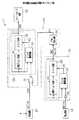
図2は、昇圧電源生成回路11の詳細を示すブロック図である。
オシレータ回路15(第2オシレータ回路)は、周期回路23、スイッチ制御回路24、及びインバータゲート25を含み、周期回路23は周期ディレイ回路21とスイッチ回路22とからなる。周期ディレイ回路21の出力信号はスイッチ回路22に入力され、スイッチ回路22の出力信号は周期ディレイ回路21に帰還されるとともにスイッチ制御回路24に入力される。
【0024】
インバータゲート25には第2検出回路13からの検出信号DET-S が入力され、そのインバータゲート25の出力信号はスイッチ制御回路24に入力される。スイッチ制御回路24は、インバータゲート25の出力信号及びオシレータ信号OSC-S に応答して活性化し、スイッチ回路22に活性化信号を出力する。スイッチ回路22は活性化信号に応答して活性化し、周期回路23はリングオシレータとして動作し、第2周波数を持つオシレータ信号OSC-S を出力する。
【0025】
不正パルス防止回路14は、パルス発生回路31、合成器32、オシレータ回路33(第1オシレータ回路)を含む。第1オシレータ回路33は、周期回路43、スイッチ制御回路44を含み、周期回路43は周期ディレイ回路41とスイッチ回路42とからなる。周期ディレイ回路41の出力信号はスイッチ回路42に入力され、スイッチ回路42の出力信号は周期ディレイ回路41に帰還されるとともにスイッチ制御回路44に入力される。
【0026】
パルス発生回路31には、第2オシレータ回路15からのオシレータ信号OSC-S が入力され、そのオシレータ信号OSC-S を受けてパルス発生回路31はパルス信号P1を出力する。合成器32には、そのパルス信号P1及び第1検出回路12からの検出信号DET-A が入力され、その合成器32の出力信号はスイッチ制御回路44に入力される。
【0027】
スイッチ制御回路44は、合成器32の出力信号及びオシレータ信号OSC に応答して活性化し、スイッチ回路42に活性化信号を出力する。スイッチ回路42は活性化信号に応答して活性化し、周期回路43はリングオシレータとして動作する。
【0028】
即ち、不正パルス防止回路14は、第1制御信号IN1として第1検出回路12からの検出信号DET-A を入力し、第2制御信号IN2として第2オシレータ回路15からのオシレータ信号OSC-S を入力する。
【0029】
そして、第1オシレータ回路33は、合成器32に例えばHレベルの検出信号DET-A が入力される時(第1制御信号IN1が第1状態の時)に活性化される。この時には、第1オシレータ回路33の周期回路43が第1周波数(第1周波数>第2周波数)にて発振する。これにより、不正パルス防止回路14から第1周波数を持つオシレータ信号OSC が出力される。
【0030】
また、後述するように第1オシレータ回路33は、合成器32に例えばLレベルの検出信号DET-A が入力される時(第1制御信号IN1が第2状態の時)には、オシレータ信号OSC-S に基づいて生成されるパルス信号P1により活性化される。この時には、不正パルス防止回路14から第2周波数の周期を持つオシレータ信号OSC が出力される。
【0031】
チャージポンプ回路16は、そのオシレータ信号OSC に基づいてチャージポンプ動作を行い、電源電圧VDD を昇圧した昇圧電圧VPP を生成する。
図3は、第1検出回路12の回路図を示す。
【0032】
第1検出回路12は、抵抗R1,R2と、カレントミラー51と、インバータ52とから構成される。
カレントミラー51は、第1及び第2のPMOSトランジスタTr1,Tr2と、第1〜第3のNMOSトランジスタTr3〜Tr5から構成される。
【0033】
カレントミラー51の一方の入力端子(図中、第1のNMOSトランジスタTr3のゲート)には、チャージポンプ回路16にて生成された昇圧電圧VPP を抵抗R1,R2にて分圧した電圧が入力される。また、カレントミラー51の他方の入力端子(図中、第2のNMOSトランジスタTr4のゲート)には、基準電圧Vrefが入力される。
【0034】
第2のPMOSトランジスタTr2には、第3のPMOSトランジスタTr6が並列に接続され、その第3のPMOSトランジスタTr6と第3のNMOSトランジスタTr5のゲートにはアクティブ時を示す活性化信号φが入力される。
【0035】
そして、第2及び第3のPMOSトランジスタTr2,Tr6、第3のNMOSトランジスタTr4のドレインから出力信号が出力され、その出力信号はインバータ52に入力される。
【0036】
そして、第1検出回路12は、アクティブ時を示す活性化信号φにより活性化されると、チャージポンプ回路16にて生成される昇圧電圧VPP を検出する。このとき、昇圧電圧VPP の分圧レベルが基準電圧Vref以下ならば、第1オシレータ回路33を活性化させる。例えば、第1検出回路12は、Hレベルの検出信号DET-A を出力する。
【0037】
図4は、第2検出回路13の回路図を示す。
上記第1検出回路12と同様に、第2検出回路13は、抵抗R3,R4と、カレントミラー61と、インバータ62とから構成される。
【0038】
カレントミラー61は、第1及び第2のPMOSトランジスタTr7,Tr8と、第1〜第3のNMOSトランジスタTr9〜Tr11から構成される。
カレントミラー61の一方の入力端子(図中、第1のNMOSトランジスタTr9のゲート)には、チャージポンプ回路16にて生成された昇圧電圧VPP を抵抗R3,R4にて分圧した電圧が入力される。また、カレントミラー61の他方の入力端子(図中、第2のNMOSトランジスタTr10のゲート)には、基準電圧Vrefが入力される。
【0039】
また、第3のNMOSトランジスタTr11のゲートに電源電圧VDD が供給される。これにより、第2検出回路13は、アクティブ時及びスタンバイ時にて電源電圧VDD が供給される限り常時活性化されている。
【0040】
従って、第2検出回路13は、アクティブ時及びスタンバイ時を問わずチャージポンプ回路16にて生成される昇圧電圧VPP を常時検出する。そして、その昇圧電圧VPP の分圧レベルが基準電圧Vref以下ならば、第2オシレータ回路15を活性化させる。例えば、第2検出回路13は、Hレベルの検出信号DET-S を出力する。
【0041】
図5は、第2オシレータ回路15の回路図を示す。
上記したように、第2オシレータ回路15は、周期回路23、スイッチ制御回路24、及びインバータゲート25を含み、周期回路23は、周期ディレイ回路21とスイッチ回路22とからなる。
【0042】
スイッチ回路22は、第1のPMOSトランジスタTr12と第1のNMOSトランジスタTr13で構成されるインバータ22aと、第2及び第3のPMOSトランジスタTr14,Tr15と、第2及び第3のNMOSトランジスタTr16,Tr17で構成される。周期ディレイ回路21は、偶数段(例えば4段)のインバータ21aにて構成されている。
【0043】
周期ディレイ回路21の出力信号(ノードN1)は、スイッチ回路22のインバータ22a(トランジスタTr12,Tr13のゲート)に入力され、インバータ22aの出力端子は周期ディレイ回路21の入力端子(初段のインバータ)に接続されている。即ち、周期回路23には、奇数段のインバータ(周期ディレイ回路21の4つのインバータ21aとスイッチ回路22のインバータ22a)を環状に接続したリングオシレータが構成される。
【0044】
第2のPMOSトランジスタTr14のソースは電源電圧VDD に接続され、ドレインはインバータ22aを構成する第1のPMOSトランジスタTr12のソースに接続される。また、第2のNMOSトランジスタTr16のソースはグランドGNDに接続され、ドレインはインバータ22aを構成する第1のNMOSトランジスタTr13のソースに接続される。従って、トランジスタTr14,Tr16がオンされると周期回路23が活性化され、周期回路23は、第2周波数を持つオシレータ信号OSC-S を出力する。
【0045】
第3のPMOSトランジスタTr15のソースは電源電圧VDD に接続され、ゲートは第2のNMOSトランジスタTr16のゲートに接続される。また、第3のNMOSトランジスタTr17のソースはグランドGNDに接続され、ゲートは第2のPMOSトランジスタTr14のゲートに接続される。
【0046】
第3のPMOSトランジスタTr15及び第3のNMOSトランジスタTr17のドレインは互いに接続され、その接続ノードN2はインバータ22aの出力端子(トランジスタTr12,Tr13のドレイン)に接続される。そして、図5に示すように、このノードN2から周期回路23の出力信号としてオシレータ信号OSC-S が出力される。
【0047】
スイッチ制御回路24は複数の論理回路により構成され、例えばインバータ24aと、ナンド回路24bと、ノア回路24cとから構成される。
インバータ24aにはインバータゲート25の出力信号(ノードN3)が入力され、そのインバータゲート25の出力信号はナンド回路24bの一方の入力端子に入力される。ナンド回路24bの他方の入力端子にはオシレータ信号OSC-S が入力される。また、そのオシレータ信号OSC-S はノア回路24cの一方の入力端子に入力され、そのノア回路24cの他方の入力端子にはインバータ24aの出力信号が入力される。
【0048】
ナンド回路24bの出力信号は、第2のNMOSトランジスタTr16及び第3のPMOSトランジスタTr15のゲートに入力される。ノア回路24cの出力信号は、第3のNMOSトランジスタTr17及び第2のPMOSトランジスタTr14のゲートに入力される。これにより、周期回路23の活性・非活性はスイッチ制御回路24により制御される。
【0049】
即ち、このように構成される第2オシレータ回路15では、そのインバータゲート25に第2検出回路13からのHレベルの検出信号DET-S が入力されると、該インバータゲート25からLレベルの出力信号が出力される。(ノードN3がLレベルになる。)これにより、ナンド回路24bからHレベル、ノア回路24cからLレベルの出力信号が出力され、前記トランジスタTr14、Tr16はオンされ、トランジスタTr15,Tr17はオフされる。従って、スイッチ回路22のインバータ22aが活性化され、周期回路23は第2周波数を持つオシレータ信号OSC-S を出力する。
【0050】
一方、インバータゲート25に第2検出回路13からのLレベルの検出信号DET-S が入力されると、該インバータゲート25からHレベルの出力信号が出力される。(ノードN3がHレベルになる。)
この際、周期回路23からLレベルのオシレータ信号OSC-S が出力されている場合には、ナンド回路24b及びノア回路24cから共にHレベルの出力信号が出力される。これにより、前記トランジスタTr14,Tr15はオフされ、トランジスタTr16,Tr17はオンされる。従って、スイッチ回路22のインバータ22aが非活性化されることにより周期回路23は動作停止する。このとき、オンしたトランジスタTr17によりオシレータ信号OSC-S はLレベルにクランプされる(グランドGNDに接続される)。
【0051】
また、上記のようにインバータゲート25からHレベルの出力信号が出力される時に、周期回路23からHレベルのオシレータ信号OSC-S が出力されている場合には、ナンド回路24b及びノア回路24cから共にLレベルの出力信号が出力される。これにより、前記トランジスタTr14,Tr15はオンされ、トランジスタTr16,Tr17はオフされる。従って、前記同様にスイッチ回路22のインバータ22aが非活性化されることにより周期回路23は動作停止する。このとき、オンしたトランジスタTr15によりオシレータ信号OSC-S はHレベルにクランプされる(電源電圧VDD に接続される)。
【0052】
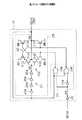
図6は、不正パルス防止回路14の回路図を示す。
上記したように、不正パルス防止回路14は、パルス発生回路31、合成器32、第1オシレータ回路33を含む。
【0053】
まず、パルス発生回路31について説明する。
パルス発生回路31は複数の論理回路により構成され、第2オシレータ回路15から出力されるオシレータ信号OSC-S (第2制御信号IN2)のパルスエッジをトリガー(エッジトリガー方式)として新たにパルスを生成する。本実施形態では、パルス発生回路31は、奇数段(例えば3段)のインバータからなる第1及び第2遅延回路71,72と、インバータ73と、第1〜第3のナンド回路74〜76とから構成されている。
【0054】
第1ナンド回路74には、オシレータ信号OSC-S が入力されるとともに、そのオシレータ信号OSC-S を第1遅延回路71にて遅延及びレベル反転させた信号が入力される。また、オシレータ信号OSC-S はインバータ73に入力され、そのインバータ73の出力信号は第2ナンド回路75に入力される。その第2ナンド回路75には、インバータ73の出力信号を第2遅延回路72にて遅延及びレベル反転させた信号が入力される。第1及び第2ナンド回路74,75の出力信号は第3ナンド回路76に入力される。
【0055】
そして、第2周波数を持つオシレータ信号OSC-S のパルスエッジ(立ち上がりエッジ、立ち下がりエッジ)に基づいて第3ナンド回路76からパルス信号P1が出力される。即ち、パルス発生回路31は、オシレータ信号OSC-S のパルスエッジに基づいて第1及び第2遅延回路71,72の遅延時間に対応するパルス幅を持つHレベルのパルス信号P1を出力する。つまり、パルス信号P1は第2周波数の2倍の周波数を持つ。
【0056】
ちなみに、後述するように、このパルス信号P1に基づいて第1オシレータ回路33の周期回路43が半周期もしくは1周期分動作する。即ち、パルス発生回路31から出力されるパルス信号P1は、周期回路43を半周期もしくは1周期動作させる時間よりも短くなるようなパルス幅を有し、このパルス幅は第1及び第2遅延回路71,72による遅延時間により設定される。
【0057】
次に、合成器32について説明する。
合成器32はノア回路で構成され、そのノア回路には、第1検出回路12からの検出信号DET-A (第1制御信号IN1)が入力されるとともに、パルス発生回路31からのパルス信号P1が入力される。これにより、合成器32は、第1検出回路12から第1オシレータ回路33を活性化させるHレベルの検出信号DET-A またはパルス発生回路31からHレベルのパルス信号P1が入力される場合に、Lレベルの出力信号を出力する。
【0058】
次に、第1オシレータ回路33について説明する。
第1オシレータ回路33は、周期回路43、スイッチ制御回路44を含み、周期回路43は周期ディレイ回路41及びスイッチ回路42からなる。即ち、第1オシレータ回路33は、上記第2オシレータ回路15と同様に構成される。
【0059】
ちなみに、第1オシレータ回路33は、周期ディレイ回路41を構成する偶数段(4段)のインバータ41aにて各インバータ41aを構成するトランジスタの素子パラメータ(例えばチャネル長)が第2オシレータ回路15の4段のインバータ21aのそれと異なる。これにより、第1オシレータ回路33は、第2オシレータ回路15が発振する第2周波数と異なる発振周波数、即ち第1周波数の周期にて発振する(第1周波数>第2周波数)。尚、第1オシレータ回路33の周期ディレイ回路41と、第2オシレータ回路15の周期ディレイ回路21とを異なる段数(偶数段)のインバータにて構成することにより、異なる発振周波数を設定することもできる。
【0060】
そして、上記第2オシレータ回路15と同様に周期回路43の活性・非活性はスイッチ制御回路44により制御され、図6に示すノードN5から周期回路43の出力信号としてオシレータ信号OSC が出力される。
【0061】
詳述すると、合成器32からLレベルの出力信号が出力されると(ノードN6がLレベルになると)、前記同様にスイッチ回路42のインバータ42aが活性化され、周期回路43は動作する。一方、合成器32からHレベルの出力信号が出力されると(ノードN6がHレベルになると)、スイッチ回路42のインバータ42aが非活性化されることにより周期回路43は動作停止する。
【0062】
この際、前記同様にして周期回路43からLレベルのオシレータ信号OSC が出力されている場合には、オンしたトランジスタTr23によりオシレータ信号OSC はLレベルにクランプされる(グランドGNDに接続される)。また、周期回路43からHレベルのオシレータ信号OSC が出力されている場合には、オンしたトランジスタTr21によりオシレータ信号OSC はHレベルにクランプされる(電源電圧VDD に接続される)。
【0063】
そして、このように構成される不正パルス防止回路14では、検出信号DET-A (第1制御信号IN1)又はオシレータ信号OSC-S (第2制御信号IN2)に基づいて第1オシレータ回路33からオシレータ信号OSC が出力される。
【0064】
詳述すると、合成器32にHレベルの検出信号DET-A が入力されるとき(アクティブ時)、スイッチ回路42のトランジスタTr20,Tr22がオンされ、トランジスタTr21,Tr23がオフされる。これにより、第1オシレータ回路33は、第1周波数を持つオシレータ信号OSC を出力する。
【0065】
また、合成器32にLレベルの検出信号DET-A が入力されるとき(スタンバイ時)、第1オシレータ回路33はパルス信号P1に応答して間欠動作する。即ち、上記したように、パルス発生回路31はオシレータ信号OSC-S のエッジをトリガーとして所定時間Hレベルのパルス信号P1を入力する。すると、合成器32からLレベルのパルス信号が出力されることにより(図8(b)参照)、上記したように第1オシレータ回路33では、スイッチ回路42のインバータ42aが活性化される。
【0066】
このとき、図8(b)に示すように、例えば第1オシレータ回路33から出力されているオシレータ信号OSC の初期状態における電圧レベルがLレベルであるときには、周期ディレイ回路41の出力(ノードN4)も同様にLレベルとなっている。従って、スイッチ回路42のインバータ42aが活性化されると、第1オシレータ回路33は直ちにHレベルのオシレータ信号OSC を出力する。合成器32からのLレベルのパルス信号は、反転したオシレータ信号OSC がノードN4に伝達される(ノードN4のレベルが周期ディレイ回路41により変更される)までにHレベルとなるため、インバータ42aは非活性化される。そして、オシレータ信号OSC を受けるスイッチ制御回路44のナンド回路44bからLレベルの信号が出力され、その信号によりオンしたトランジスタTr21によってオシレータ信号OSC はHレベルにクランプされる。即ち、第1オシレータ回路33の周期回路43が、結果として半周期動作した状態となる。
【0067】
次いで、再度、Hレベルのパルス信号P1を受けて合成器32からLレベルのパルス信号が出力されたときには、前記オシレータ信号OSC はHレベルにクランプされているため、周期ディレイ回路41の出力(ノードN4)も同様にHレベルとなっている。従って、スイッチ回路42のインバータ42aが活性化されると、第1オシレータ回路33は直ちにLレベルのオシレータ信号OSC を出力する。合成器32からのLレベルのパルス信号は、反転したオシレータ信号OSC がノードN4に伝達される(ノードN4のレベルが周期ディレイ回路41により変更される)までにHレベルとなるため、インバータ42aは非活性化される。そして、オシレータ信号OSC を受けるスイッチ制御回路44のノア回路44cからHレベルの信号が出力され、その信号によりオンしたトランジスタTr23によってオシレータ信号OSC はLレベルにクランプされる。即ち、前記同様に第1オシレータ回路33の周期回路43が、結果として半周期動作した状態となる。
【0068】
このように、第1オシレータ回路33のオシレータ信号OSC は、合成器32にLレベルの検出信号DET-A が入力されている状態では(スタンバイ時)、第2オシレータ信号OSC-S の第2周波数の周期と同じ周期で発振する。
【0069】
尚、本実施形態では、パルス発生回路31からのパルス信号P1に応答して第1オシレータ回路33の周期回路43が半周期動作するように構成されるが、1周期動作するように構成されてもよい。
【0070】
図7は、チャージポンプ回路16の回路図を示す。
チャージポンプ回路16は、ダイオードとして機能するトランジスタTr24,Tr25と容量C1とから構成され、それらトランジスタTr24,Tr25の接続ノードN7に容量C1の出力端子が接続される。
【0071】
容量C1の入力端子にはオシレータ信号OSC が入力される。トランジスタTr24,Tr25は、例えばNMOSトランジスタのゲートをドレインに接続したMOSダイオードであり、トランジスタTr24のドレインに電源電圧VDD に接続され、トランジスタTr25のソースから昇圧電圧VPP が出力される。
【0072】
このようなチャージポンプ回路16では、Lレベルのオシレータ信号OSC が入力されると、容量C1に電源電圧VDD から電荷が充電され、その結果ノードN7は電源電圧VDD の電圧よりもトランジスタTr24の閾値だけ低い電圧となる。
【0073】
次いで、Hレベルのオシレータ信号OSC が入力されると、ノードN7は容量C1の容量結合により昇圧される。そして、ノードN7の電圧が、昇圧電圧VPP の電圧よりもトランジスタTr25の閾値以上高くなると、容量C1から電荷が供給されて昇圧電圧VPP は昇圧される。
【0074】
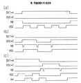
このように、Hレベル又はLレベルのオシレータ信号OSC が繰り返し入力されることにより、チャージポンプ回路16が動作して昇圧電圧VPP が生成される。次に、上記のように構成される昇圧電源生成回路11の作用について図8に従って説明する。
【0075】
図8(a)に示すように、第1検出回路12からアクティブモードを示すHレベルの検出信号DET-A が出力されると、図6に示すノードN6(合成器32の出力信号)がLレベルとなる。これにより、第1オシレータ回路33は第1周波数の周期にて発振し、オシレータ信号OSC を出力する。その後、第1検出回路12からLレベルの検出信号DET-A が出力されてアクティブモードが解除されると、ノードN6がHレベルとなり第1オシレータ回路33は不活性化される。このとき、オシレータ信号OSC はHレベルにクランプされる。
【0076】
次いで、図8(b)に示すように、第1検出回路12からLレベルの検出信号DET-A が出力されている時に、第2オシレータ回路15からオシレータ信号OSC-S のパルスが入力されると、上記したようにノードN6にLレベルのパルスが発生する。このとき、Lレベルのパルスは、第2周波数の周期を持つオシレータ信号OSC-S のパルスエッジに基づいて発生する。従って、上記したように第1オシレータ回路33は、第2オシレータ信号OSC-S の第2周波数の周期と同じ周期で発振する。
【0077】
次に、第1検出回路12からLレベルの検出信号DET-A が出力された後(アクティブモードが解除後)の短い期間にオシレータ信号OSC-S のパルスが入力される場合について説明する。
【0078】
図8(c)に示すように、今、第1オシレータ回路33は、Hレベルの検出信号DET-A により第1周波数の周期を持つオシレータ信号OSC を出力している。
次いで、第1オシレータ回路33にLレベルの検出信号DET-A が入力されると、ノードN6がHレベルとなり第1オシレータ回路33は不活性化される。このとき、オシレータ信号OSC はLレベルにクランプされる。
【0079】
今ここで、Lレベルの検出信号DET-A に切り替わり後、直ちにオシレータ信号OSC-S のパルスが入力されるとする(図では、Hレベルに立ち上がる)。
すると、前記同様にしてノードN6にLレベルのパルスが発生することにより、第1オシレータ回路33にてスイッチ回路42のインバータ42aが活性化され、オシレータ信号OSC は、そのLレベルのクランプが解除される。しかし、このときノードN4(周期ディレイ回路41の出力信号)は、Lレベルのオシレータ信号OSC が周期ディレイ回路41にて遅延されるため、未だHレベルとなっている。このため、第1オシレータ回路33はLレベルのオシレータ信号OSC を出力する。さらに、図8(c)に示すように、ノードN6に発生するLレベルのパルスは短い期間に立ち上がるため、ノードN4が立ち下がる前にスイッチ回路42のインバータ42aが不活性化される。つまり、Lレベルのオシレータ信号OSC の状態で、周期回路43の動作が停止する。
【0080】
これにより、第1オシレータ回路33からのオシレータ信号OSC のパルス幅は、該第1オシレータ回路33が発振する第1周波数の周期よりも短いパルス幅にならない。ちなみに、このことは第2オシレータ回路15からオシレータ信号OSC-S のパルスが入力された後、直ちにHレベルの検出信号DET-A が入力される場合にも同様なことがいえる。
【0081】
図9は、不正パルス防止回路14の入出力特性を示す。
上記のように構成される昇圧電源生成回路11では、第2制御信号IN2として入力される入力周波数(オシレータ信号OSC-S )により、不正パルス防止回路14から出力されるオシレータ信号OSC は第1周波数より低い周波数を出力する。
【0082】
以上記述したように、本実施形態によれば、以下の効果を奏する。
(1)不正パルス防止回路14は、パルス発生回路31、合成器32、第1オシレータ回路33を含み、その第1オシレータ回路33は、周期ディレイ回路41とスイッチ回路42とからなる周期回路43、スイッチ制御回路44を含む。第1オシレータ回路33は、アクティブ時には合成器32に入力される検出信号DET-A に基づいて第1周波数を持つオシレータ信号OSC を出力する。また、第1オシレータ回路33は、スタンバイ時にはパルス発生回路31を介して入力される第2オシレータ回路15からのオシレータ信号OSC-S により、該オシレータ信号OSC-S の第2周波数(第1周波数>第2周波数)の周期と同じ周期で発振する。これにより、不正パルス防止回路14から第1周波数の周期より短いパルス幅をもつオシレータ信号OSC は出力されない。従って、チャージポンプ回路16のチャージポンプ動作が安定され、安定的且つ効率良く昇圧電圧VPP を供給することができる。
【0083】
(2)アクティブ時とスタンバイ時との切り替わり時や、検出信号DET-A (第1制御信号IN1)とオシレータ信号OSC-S (第2制御信号IN2)が重なって変化した場合にも第1周波数の周期より短いパルス幅をもつオシレータ信号OSC が出力されない。
【0084】
(3)互いに非同期で動作する第1及び第2オシレータ回路15,33を1つのチャージポンプにて利用する構成であるため、ダイサイズを大きくすることもない。
【0085】
(第二実施形態)
以下、本発明を例えば半導体装置に搭載される昇圧電源生成回路に具体化した第二実施形態を図10及び図11に従って説明する。
【0086】
尚、説明の便宜上、第一実施形態と同様の構成、信号については同一の符号を付してその説明を一部省略する。
図10は、本実施形態の昇圧電源生成回路を示す概略ブロック図である。
【0087】
昇圧電源生成回路81は、第1及び第2検出回路12,13と、第1オシレータ回路33を含む不正パルス防止回路82と、第2オシレータ回路15と、第3オシレータ回路83と、チャージポンプ回路16とを備える。即ち、本実施形態では、第1検出回路12の検出信号DET-A が第3オシレータ回路83に入力され、その第3オシレータ回路83のオシレータ信号OSC-A が第1制御信号IN1として不正パルス防止回路82に入力される。
【0088】
第3オシレータ回路83は、上記第2オシレータ回路15と同様な回路構成をなし、その詳細な説明を省略する。尚、本実施形態では、第3オシレータ回路83は第3周波数の周期にて発振し、その第3周波数の周期は、第1オシレータ回路33にて発振する第1周波数の周期より長い周期を持つ。また、第3周波数の周期は、第2オシレータ回路15にて発振する第2周波数の周期より短い周期を持つ。つまり、第1周波数>第3周波数>第2周波数である。
【0089】
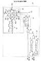
図11は、不正パルス防止回路82の回路図を示す。
不正パルス防止回路82は、第1及び第2パルス発生回路31a,31b、合成器32、周期回路43、スイッチ制御回路44を備える。第1及び第2パルス発生回路31a,31bは、図6に示す上記第一実施形態の不正パルス防止回路14のパルス発生回路31と同じ構成を持つ。従って、第1制御信号IN1を受ける第1パルス発生回路31aから出力されるパルス信号と、第2制御信号IN2を受ける第2パルス発生回路31bから出力されるパルス信号が合成器32に入力されるようにして構成されている。尚、本実施形態では、第1制御信号IN1はオシレータ信号OSC-A であり、第2制御信号IN2はオシレータ信号OSC-S である。
【0090】
次に、このように構成される昇圧電源生成回路81の作用について説明する。上記同様にして第1検出回路12は、アクティブ時に昇圧電圧VPP を検出し、その分圧レベルが基準電圧Vref以下であるとHレベルの検出信号DET-A を出力し、その検出信号DET-A は第3オシレータ回路83に入力される。第3オシレータ回路83は、Hレベルの検出信号DET-A を受けて第3周波数にて発振し、その周期を持つオシレータ信号OSC-A を出力する。
【0091】
すると、不正パルス防止回路82には、その合成器32にオシレータ信号OSC-A が第1パルス発生回路31aを介して入力されることにより、上記第一実施形態と同様にして第1オシレータ回路33が第3周波数の周期と同じ周期にて発振するようになる。従って、不正パルス防止回路82から第3周波数の周期と同じ周期を持つオシレータ信号OSC が出力される。
【0092】
これにより、チャージポンプ回路16では、上記第一実施形態のように電源電圧VDD から電荷が供給され、次第に昇圧電圧VPP が生成される。そして、第1検出回路12は、昇圧電圧VPP の分圧レベルが基準電圧Vref以上となるとLレベルの検出信号DET-A を出力し、これにより第3オシレータ回路83が不活性化され、不正パルス防止回路82も不活性化する。従って、チャージポンプ回路16は動作を停止する。
【0093】
一方、第2検出回路13は、常時昇圧電圧VPP を検出し、その分圧レベルが基準電圧Vref以下であるとHレベルの検出信号DET-S を出力し、その検出信号DET-S は第2オシレータ回路15に入力される。第2オシレータ回路15は、Hレベルの検出信号DET-S を受けて第2周波数にて発振し、その周期を持つオシレータ信号OSC-S を出力する。
【0094】
すると、不正パルス防止回路82には、その合成器32にオシレータ信号OSC-S が第2パルス発生回路31bを介して入力されることにより、上記第一実施形態と同様にして第1オシレータ回路33が第2周波数の周期と同じ周期にて発振するようになる。従って、不正パルス防止回路82から第2周波数の周期と同じ周期を持つオシレータ信号OSC が出力される。
【0095】
これにより、チャージポンプ回路16では、上記第一実施形態のように電源電圧VDD から電荷が供給され、次第に昇圧電圧VPP が生成される。そして、第2検出回路13は、昇圧電圧VPP の分圧レベルが基準電圧Vref以上となるとLレベルの検出信号DET-S を出力し、これにより第2オシレータ回路15が不活性化され、不正パルス防止回路82も不活性化する。従って、チャージポンプ回路16は動作を停止する。
【0096】
以上記述したように、本実施形態によれば、不正パルス防止回路82のオシレータ信号OSC の状態は、第1及び第2制御信号IN1,IN2(オシレータ信号OSC-A ,OSC-S )の切り替わり毎に切り替えられる。従って、上記第一実施形態と同様な効果を奏することができる。
【0097】
尚、前記各実施形態は、以下の態様に変更してもよい。
・リングオシレータを構成する周期回路43にて、周期ディレイ回路41の4つのインバータ41aは例えば2又は6つの偶数段のインバータでもよい。即ち、スイッチ回路42のインバータ42aとを合わせた奇数段のインバータによりリングオシレータを構成してもよい。
【0098】
・第1オシレータ回路33の周期ディレイ回路41と、第2オシレータ回路15の周期ディレイ回路21とを異なる段数のインバータにて構成することにより、異なる発振周波数を持つようにすることもできる。
【0099】
・例えばSDRAM等のメモリデバイスにおいて、第1制御信号IN1としてシステムクロックを入力し、第2制御信号IN2としてセルフリフレッシュの要求信号を入力するようにしてもよい。
【0100】
・上記各実施形態では、昇圧電源生成回路11,81に具体化したが、負電源生成回路に具体化してもよい。
以上の様々な実施形態をまとめると、以下のようになる。
(付記1) 周期ディレイ回路と該周期ディレイ回路のループを制御するスイッチ回路とを有する周期回路を備え、第1制御信号又は第2制御信号に基づいて第1周波数又は第2周波数のオシレータ信号を生成するオシレータ回路の制御方法であって、
前記第1制御信号が第1状態の時に、該第1制御信号に基づいて前記第1周波数を発振させ、前記第1制御信号が第2状態の時に、前記オシレータ信号を前記第2制御信号の周期に同期させるようにしたことを特徴とするオシレータ回路の制御方法。
(付記2) 前記スイッチ回路を活性化して前記周期回路を半周期もしくは1周期動作させる第1ステップと、
前記スイッチ回路を非活性化させる第2ステップと
を前記第1制御信号が第2状態の時に実行することを特徴とする付記1に記載のオシレータ回路の制御方法。
(付記3) 周期ディレイ回路と該周期ディレイ回路のループを制御するスイッチ回路とを有する周期回路を備え、第1制御信号又は第2制御信号に基づいて第1周波数又は第2周波数のオシレータ信号を生成するオシレータ回路の制御方法であって、
前記オシレータ信号を前記第1又は第2制御信号の周期に同期させるようにしたことを特徴とするオシレータ回路の制御方法。
(付記4) 周期ディレイ回路と該周期ディレイ回路のループを制御するスイッチ回路とを有する周期回路を備え、第1制御信号又は第2制御信号に基づいて第1周波数又は第2周波数のオシレータ信号を生成するオシレータ回路であって、前記第2制御信号の変位に基づいて前記周期回路を半周期もしくは1周期動作させるパルス信号を生成するパルス発生回路と、
前記第1制御信号及び前記パルス発生回路の出力信号を入力する合成器と、
前記合成器の出力信号に基づいて前記スイッチ回路を制御するスイッチ制御回路と
を備えたことを特徴とするオシレータ回路。
(付記5) 前記パルス発生回路には、
前記第1周波数の周波数より低い前記第2周波数を、前記第2制御信号として入力したことを特徴とする付記4に記載のオシレータ回路。
(付記6) 周期ディレイ回路と該周期ディレイ回路のループを制御するスイッチ回路とを有する周期回路を備え、第1制御信号又は第2制御信号に基づいて第1周波数又は第2周波数のオシレータ信号を生成するオシレータ回路であって、
前記第1制御信号の変位に基づいて前記周期回路を半周期もしくは1周期動作させるパルス信号を生成する第1パルス発生回路と、
前記第2制御信号の変位に基づいて前記周期回路を半周期もしくは1周期動作させるパルス信号を生成する第2パルス発生回路と、
前記第1及び第2パルス発生回路の各出力信号を入力する合成器と、
前記合成器の出力信号に基づいて前記スイッチ回路を制御するスイッチ制御回路と
を備えたことを特徴とするオシレータ回路。
(付記7) 前記第1及び第2パルス発生回路には、
前記第1周波数の周波数より低く、且つ互いに異なる周波数である2つのオシレータ信号をそれぞれ入力したことを特徴とする付記6に記載のオシレータ回路。
(付記8) 前記パルス発生回路は、
該パルス発生回路に入力される前記制御信号の変位に基づいて前記周期回路を半周期もしくは1周期動作させる時間よりも短いパルス幅を有する前記パルス信号を生成することを特徴とする付記4又は6に記載のオシレータ回路。
(付記9) 周期ディレイ回路と該周期ディレイ回路のループを制御するスイッチ回路とを有する周期回路と、前記スイッチ回路を制御するスイッチ制御回路とから構成され、第1制御信号又は第2制御信号に基づいて第1周波数又は第2周波数のオシレータ信号を生成する第1オシレータ回路と、前記オシレータ信号により駆動され、第1電圧を生成するチャージポンプ回路とを備え、
前記第1オシレータ回路を制御する第1制御信号及び第2制御信号を入力し、前記第1制御信号が第1状態の時に、該第1制御信号に基づいて前記第1オシレータ回路を前記第1周波数にて発振させ、前記第1制御信号が第2状態の時に、前記第1オシレータ回路の出力信号を前記第2制御信号の周期に同期させるようにしたことを特徴とする内部電源生成回路の制御方法。
(付記10) 前記スイッチ回路を活性化して前記周期回路を半周期もしくは1周期動作させる第1ステップと、
前記スイッチ回路を非活性化させる第2ステップと
を前記第1制御信号が第2状態の時に実行することを特徴とする付記9に記載の内部電源生成回路の制御方法。
(付記11) 周期ディレイ回路と該周期ディレイ回路のループを制御するスイッチ回路とを有する周期回路と、前記スイッチ回路を制御するスイッチ制御回路とから構成され、第1制御信号又は第2制御信号に基づいて第1周波数又は第2周波数のオシレータ信号を生成する第1オシレータ回路と、前記オシレータ信号により駆動され、第1電圧を生成するチャージポンプ回路とを備え、
前記第1オシレータ回路を制御する第1制御信号及び第2制御信号を入力し、前記第1オシレータ回路の出力信号を前記第1又は第2制御信号の周期に同期させるようにしたことを特徴とする内部電源生成回路の制御方法。
(付記12) 周期ディレイ回路と該周期ディレイ回路のループを制御するスイッチ回路とを有する周期回路と、前記スイッチ回路を制御するスイッチ制御回路とから構成され、第1制御信号又は第2制御信号に基づいて第1周波数又は第2周波数のオシレータ信号を生成する第1オシレータ回路と、
前記オシレータ信号により駆動され、第1電圧を生成するチャージポンプ回路と、
前記第2制御信号の変位に基づいて前記周期回路を半周期もしくは1周期動作させるパルス信号を生成するパルス発生回路と、
前記第1制御信号、及び前記パルス発生回路の出力信号を入力する合成器と
を備えたことを特徴とする内部電源生成回路。
(付記13) 前記パルス発生回路には、
前記第1周波数の周波数より低い前記第2周波数を持つ第2オシレータ回路の出力信号を前記第2制御信号として入力したことを特徴とする付記12に記載の内部電源生成回路。
(付記14) 周期ディレイ回路と該周期ディレイ回路のループを制御するスイッチ回路とを有する周期回路と、前記スイッチ回路を制御するスイッチ制御回路とから構成され、第1制御信号又は第2制御信号に基づいて第1周波数又は第2周波数のオシレータ信号を生成する第1オシレータ回路と、
前記オシレータ信号により駆動され、第1電圧を生成するチャージポンプ回路と、
前記第1制御信号の変位に基づいて前記周期回路を半周期もしくは1周期動作させるパルス信号を生成する第1パルス発生回路と、
前記第2制御信号の変位に基づいて前記周期回路を半周期もしくは1周期動作させるパルス信号を生成する第2パルス発生回路と、
前記第1及び第2パルス発生回路の各出力信号を入力する合成器と
を備えたことを特徴とする内部電源生成回路。
(付記15) 前記第1及び第2パルス発生回路には、
前記第1周波数の周波数より低く、且つ互いに異なる周波数である2つのオシレータ回路の出力信号をそれぞれ入力したことを特徴とする付記14に記載の内部電源生成回路。
(付記16) 前記パルス発生回路は、
該パルス発生回路に入力される前記制御信号の変位に基づいて前記周期回路を半周期もしくは1周期動作させる時間よりも短いパルス幅を有する前記パルス信号を生成することを特徴とする付記12又は14に記載の内部電源生成回路。
(付記17) 前記第1電圧の電圧レベルを検出し、その検出結果に基づいて前記第1制御信号を活性化信号に制御する第1検出回路と、
前記第1電圧の電圧レベルを検出し、その検出結果に基づいて前記第2制御信号を活性化信号に制御する第2検出回路と
を備えたことを特徴とする付記12又は14に記載の内部電源生成回路。
【0101】
【発明の効果】
以上詳述したように、本発明は安定的且つ効率良く内部電源を供給し得るオシレータ回路、及び内部電源生成回路を提供することができる。
【図面の簡単な説明】
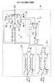
【図1】 第一実施形態の昇圧電源生成回路を示す概略ブロック図である。
【図2】 昇圧電源生成回路の詳細を示すブロック図である。
【図3】 第1検出回路を示す回路図である。
【図4】 第2検出回路を示す回路図である。
【図5】 第2オシレータ回路を示す回路図である。
【図6】 不正パルス防止回路を示す回路図である。
【図7】 チャージポンプ回路を示す回路図である。
【図8】 第一実施形態を示す波形図である。
【図9】 第一実施形態の入出力特性を示す説明図である。
【図10】 第二実施形態の昇圧電源生成回路を示す概略ブロック図である。
【図11】 不正パルス防止回路を示す回路図である。
【図12】 従来の昇圧電源生成回路を示すブロック図である。
【符号の説明】
16 チャージポンプ回路
31 パルス発生回路
33 第1オシレータ回路
41 周期ディレイ回路
42 スイッチ回路
43 周期回路
44 スイッチ制御回路
VPP 第1電圧(昇圧電圧)
IN1 第1制御信号
IN2 第2制御信号
DET-A 第1制御信号としての検出信号
OSC-S 第2制御信号としてのオシレータ信号
OSC-A 第1制御信号としてのオシレータ信号[0001]
BACKGROUND OF THE INVENTION
This inventionTheScillator timesRoad,And an internal power generation circuit.
[0002]
Semiconductor devices include a boost power supply generation circuit that generates a boost voltage to a word line or the like in a memory device such as a DRAM, and a negative power supply generation circuit that generates a voltage lower than a ground voltage used for a substrate power supply. An internal power generation circuit is provided. The internal power generation circuit has an active mode with a large driving capability for supplying internal power and a standby mode with a small driving capability, and reduces current consumption in the standby mode. In recent years, semiconductor devices are increasingly required to stabilize operation as well as to reduce power consumption in response to portable information terminals driven by batteries.
[0003]
[Prior art]
FIG. 12 shows a conventional internal power generation circuit mounted on a semiconductor device. This internal power supply generation circuit is a boost power supply generation circuit that generates a boosted voltage VPP obtained by boosting an external or internal power supply voltage VDD.
[0004]
The boost power
[0005]
First, the active mode will be described.
The
[0006]
The
[0007]
Next, the standby mode will be described.
The
[0008]
The
[0009]
As described above, the boost power
[0010]
[Problems to be solved by the invention]
By the way, in the boost power
[0011]
For this reason, a method is conceivable in which the boost power
[0012]
However, since the charge pump circuit generally has a large circuit area, this method has been a factor of increasing the die size and a factor of increasing power consumption.
[0013]
An object of the present invention is to supply an internal power source stably and efficiently.RuoScillator timesRoad,And providing an internal power generation circuit.
[0014]
[Means for Solving the Problems]
[0015]
According to the first aspect of the present invention, the first oscillator circuit includes a first period circuit having a first period delay circuit and a first switch circuit that controls a loop of the first period delay circuit. An oscillator signal having a first frequency is generated based on the control signal. The second oscillator circuit includes a second period circuit having a second period delay circuit and a second switch circuit for controlling a loop of the second period delay circuit, and a second switch control circuit for controlling the second switch circuit. And generating an oscillator of the second frequency based on the second control signal. The pulse generation circuit receives the oscillator signal of the second frequency, andOf the second frequencyBased on the displacement of the oscillator signal, a pulse signal is generated for operating the first periodic circuit that oscillates at the first frequency for a half period or one period. The synthesizer is connected to the output of the pulse generation circuit, and receives the first control signal and the pulse signal and outputs an output signal to the first switch control circuit.
[0016]
Claim2According to the invention described inThe first frequency is greater than the second frequency.
[0017]
According to a third aspect of the present invention, the first oscillator circuit includes a first period circuit having a first period delay circuit and a first switch circuit that controls a loop of the first period delay circuit, A first oscillator signal having a first frequency is generated based on the control signal. The second oscillator circuit includes a second period circuit having a second period delay circuit and a second switch circuit for controlling a loop of the second period delay circuit, and a second switch control circuit for controlling the second switch circuit. And generating a second oscillator of the second frequency based on the second control signal. The pulse generation circuit of the internal power generation circuit includes the first power generation circuit.2A scintillator signal is input,SecondBased on the displacement of the oscillator signal, a pulse signal is generated for operating the first periodic circuit that oscillates at the first frequency for a half period or one period. The synthesizer of the internal power supply circuit is connected to the output of the pulse generation circuit, and receives the first control signal and the pulse signal and outputs an output signal to the first switch control circuit. The charge pump circuit is driven by the first oscillator signal to generate a first voltage.
According to the invention of claim 4, the first frequency is higher than the second frequency.
[0018]
DETAILED DESCRIPTION OF THE INVENTION
(First embodiment)
Hereinafter, a first embodiment in which the present invention is embodied in, for example, a boosted power generation circuit mounted on a semiconductor device will be described with reference to FIGS.
[0019]
FIG. 1 is a schematic block diagram of a boost power supply generation circuit.
The step-up power
[0020]
The step-up power
[0021]
The
[0022]
The
[0023]
FIG. 2 is a block diagram showing details of the boost power
The oscillator circuit 15 (second oscillator circuit) includes a
[0024]
The detection signal DET-S from the
[0025]
The illegal
[0026]
The
[0027]
The
[0028]
That is, the illegal
[0029]
The
[0030]
As will be described later, the
[0031]
The
FIG. 3 shows a circuit diagram of the
[0032]
The
The
[0033]
A voltage obtained by dividing the boosted voltage VPP generated by the
[0034]
A third PMOS transistor Tr6 is connected in parallel to the second PMOS transistor Tr2, and an activation signal φ indicating an active state is input to the gates of the third PMOS transistor Tr6 and the third NMOS transistor Tr5. The
[0035]
An output signal is output from the drains of the second and third PMOS transistors Tr 2 and Tr 6 and the third NMOS transistor Tr 4, and the output signal is input to the
[0036]
The
[0037]
FIG. 4 is a circuit diagram of the
Similar to the
[0038]
The
A voltage obtained by dividing the boosted voltage VPP generated by the
[0039]
The power supply voltage VDD is supplied to the gate of the third NMOS transistor Tr11. As a result, the
[0040]
Therefore, the
[0041]
FIG. 5 shows a circuit diagram of the
As described above, the
[0042]
The
[0043]
The output signal (node N1) of the
[0044]
The source of the second PMOS transistor Tr14 is connected to the power supply voltage VDD, and the drain is connected to the source of the first PMOS transistor Tr12 constituting the inverter 22a. The source of the second NMOS transistor Tr16 is connected to the ground GND, and the drain is connected to the source of the first NMOS transistor Tr13 constituting the inverter 22a. Therefore, when the transistors Tr14 and Tr16 are turned on, the
[0045]
The source of the third PMOS transistor Tr15 is connected to the power supply voltage VDD, and the gate is connected to the gate of the second NMOS transistor Tr16. The source of the third NMOS transistor Tr17 is connected to the ground GND, and the gate is connected to the gate of the second PMOS transistor Tr14.
[0046]
The drains of the third PMOS transistor Tr15 and the third NMOS transistor Tr17 are connected to each other, and the connection node N2 is connected to the output terminal of the inverter 22a (the drains of the transistors Tr12 and Tr13). As shown in FIG. 5, the oscillator signal OSC-S is output as an output signal of the
[0047]
The
The output signal (node N3) of the
[0048]
The output signal of the
[0049]
That is, in the
[0050]
On the other hand, when the L level detection signal DET-S from the
At this time, when the L level oscillator signal OSC-S is output from the
[0051]
As described above, when the H-level oscillator signal OSC-S is output from the
[0052]
FIG. 6 shows a circuit diagram of the illegal
As described above, the illegal
[0053]
First, the
The
[0054]
The
[0055]
The
[0056]
Incidentally, as will be described later, the
[0057]
Next, the
The
[0058]
Next, the
The
[0059]
Incidentally, in the
[0060]
Similarly to the
[0061]
More specifically, when an L level output signal is output from the synthesizer 32 (when the node N6 becomes L level), the
[0062]
At this time, when the oscillator circuit OSC at the L level is output from the
[0063]
In the illegal
[0064]
More specifically, when the H level detection signal DET-A is input to the synthesizer 32 (when active), the transistors Tr20 and Tr22 of the
[0065]
Further, when the L level detection signal DET-A is input to the synthesizer 32 (during standby), the
[0066]
At this time, as shown in FIG. 8B, for example, when the voltage level in the initial state of the oscillator signal OSC output from the
[0067]
Next, when the pulse signal P1 at H level is received again and the pulse signal at L level is output from the
[0068]
As described above, the oscillator signal OSC of the
[0069]
In the present embodiment, the
[0070]
FIG. 7 shows a circuit diagram of the
The
[0071]
The oscillator signal OSC is input to the input terminal of the capacitor C1. The transistors Tr24 and Tr25 are, for example, MOS diodes in which the gate of an NMOS transistor is connected to the drain, the drain of the transistor Tr24 is connected to the power supply voltage VDD, and the boosted voltage VPP is output from the source of the transistor Tr25.
[0072]
In such a
[0073]
Next, when an H level oscillator signal OSC is input, the node N7 is boosted by capacitive coupling of the capacitor C1. Then, when the voltage at the node N7 becomes higher than the voltage of the boosted voltage VPP by the threshold value of the transistor Tr25, charges are supplied from the capacitor C1 and the boosted voltage VPP is boosted.
[0074]
As described above, when the H level or L level oscillator signal OSC is repeatedly input, the
[0075]
As shown in FIG. 8A, when the H detection signal DET-A indicating the active mode is output from the
[0076]
Next, as shown in FIG. 8B, when the L level detection signal DET-A is output from the
[0077]
Next, a case where the pulse of the oscillator signal OSC-S is input in a short period after the L level detection signal DET-A is output from the first detection circuit 12 (after the active mode is canceled) will be described.
[0078]
As shown in FIG. 8C, the
Next, when the L level detection signal DET-A is input to the
[0079]
Now, assume that the pulse of the oscillator signal OSC-S is input immediately after switching to the L level detection signal DET-A (in the figure, rises to the H level).
Then, an L level pulse is generated at the node N6 in the same manner as described above, whereby the
[0080]
As a result, the pulse width of the oscillator signal OSC from the
[0081]
FIG. 9 shows the input / output characteristics of the illegal
In the boosted power
[0082]
As described above, according to the present embodiment, the following effects can be obtained.
(1) The illegal
[0083]
(2) The first frequency even when switching between active and standby, or when the detection signal DET-A (first control signal IN1) and the oscillator signal OSC-S (second control signal IN2) change due to overlap. Oscillator signal OSC with a pulse width shorter than this period is not output.
[0084]
(3) Since the first and
[0085]
(Second embodiment)
Hereinafter, a second embodiment in which the present invention is embodied in, for example, a boosted power generation circuit mounted in a semiconductor device will be described with reference to FIGS.
[0086]
For the convenience of explanation, the same configurations and signals as those in the first embodiment are denoted by the same reference numerals, and a part of the explanation is omitted.
FIG. 10 is a schematic block diagram showing the boost power supply generation circuit of the present embodiment.
[0087]
The boosting
[0088]
The
[0089]
FIG. 11 shows a circuit diagram of the illegal
The illegal
[0090]
Next, the operation of the boost power
[0091]
Then, when the oscillator signal OSC-A is input to the
[0092]
As a result, in the
[0093]
On the other hand, the
[0094]
Then, when the oscillator signal OSC-S is input to the
[0095]
As a result, in the
[0096]
As described above, according to the present embodiment, the state of the oscillator signal OSC of the illegal
[0097]
In addition, you may change each said embodiment into the following aspects.
In the
[0098]
By configuring the
[0099]
For example, in a memory device such as an SDRAM, a system clock may be input as the first control signal IN1, and a self-refresh request signal may be input as the second control signal IN2.
[0100]
In each of the above embodiments, the boosted power
The various embodiments described above are summarized as follows.
(Supplementary Note 1) A periodic circuit having a periodic delay circuit and a switch circuit that controls a loop of the periodic delay circuit is provided, and an oscillator signal having a first frequency or a second frequency is generated based on the first control signal or the second control signal. A method for controlling an oscillator circuit to be generated, comprising:
When the first control signal is in the first state, the first frequency is oscillated based on the first control signal, and when the first control signal is in the second state, the oscillator signal is transmitted to the second control signal. A method of controlling an oscillator circuit, wherein the method is synchronized with a cycle.
(Supplementary Note 2) A first step of activating the switch circuit to operate the periodic circuit in a half cycle or one cycle;
A second step of deactivating the switch circuit;
2. The method of controlling an oscillator circuit according to
(Supplementary Note 3) A periodic circuit having a periodic delay circuit and a switch circuit for controlling a loop of the periodic delay circuit is provided, and an oscillator signal having a first frequency or a second frequency is generated based on the first control signal or the second control signal. A method for controlling an oscillator circuit to be generated, comprising:
A method of controlling an oscillator circuit, wherein the oscillator signal is synchronized with a cycle of the first or second control signal.
(Supplementary Note 4) A periodic circuit having a periodic delay circuit and a switch circuit for controlling a loop of the periodic delay circuit is provided, and an oscillator signal having a first frequency or a second frequency is generated based on the first control signal or the second control signal. A pulse generation circuit for generating a pulse signal for generating a pulse signal for operating the periodic circuit in a half cycle or in one cycle based on a displacement of the second control signal;
A synthesizer for inputting the first control signal and the output signal of the pulse generation circuit;
A switch control circuit for controlling the switch circuit based on an output signal of the combiner;
An oscillator circuit comprising:
(Supplementary Note 5) The pulse generation circuit includes:
The oscillator circuit according to appendix 4, wherein the second frequency lower than the first frequency is input as the second control signal.
(Supplementary Note 6) A periodic circuit having a periodic delay circuit and a switch circuit for controlling a loop of the periodic delay circuit is provided, and an oscillator signal having a first frequency or a second frequency is generated based on the first control signal or the second control signal. An oscillator circuit to generate,
A first pulse generating circuit for generating a pulse signal for operating the periodic circuit in a half cycle or in one cycle based on the displacement of the first control signal;
A second pulse generating circuit for generating a pulse signal for operating the periodic circuit in a half cycle or in one cycle based on the displacement of the second control signal;
A synthesizer for inputting the output signals of the first and second pulse generation circuits;
A switch control circuit for controlling the switch circuit based on an output signal of the combiner;
An oscillator circuit comprising:
(Supplementary Note 7) The first and second pulse generation circuits include
The oscillator circuit according to appendix 6, wherein two oscillator signals having frequencies lower than the first frequency and different from each other are respectively input.
(Supplementary Note 8) The pulse generation circuit includes:
The pulse signal having the pulse width shorter than the time during which the periodic circuit is operated in a half cycle or one cycle is generated based on the displacement of the control signal input to the pulse generation circuit. The oscillator circuit described in 1.
(Additional remark 9) It is comprised from the periodic circuit which has a period delay circuit and the switch circuit which controls the loop of this period delay circuit, and the switch control circuit which controls the said switch circuit, and is used as a 1st control signal or a 2nd control signal. A first oscillator circuit that generates an oscillator signal having a first frequency or a second frequency based on the first oscillator circuit, and a charge pump circuit that is driven by the oscillator signal and generates a first voltage,
A first control signal and a second control signal for controlling the first oscillator circuit are input, and when the first control signal is in the first state, the first oscillator circuit is set to the first control signal based on the first control signal. An internal power generation circuit characterized by oscillating at a frequency and synchronizing the output signal of the first oscillator circuit with the period of the second control signal when the first control signal is in the second state. Control method.
(Supplementary Note 10) A first step of activating the switch circuit to operate the periodic circuit in a half cycle or one cycle;
A second step of deactivating the switch circuit;
The control method of the internal power generation circuit according to appendix 9, wherein the first control signal is executed when the first control signal is in the second state.
(Additional remark 11) It is comprised from the periodic circuit which has a periodic delay circuit and the switch circuit which controls the loop of this periodic delay circuit, and the switch control circuit which controls the said switch circuit, and is used as a 1st control signal or a 2nd control signal. A first oscillator circuit that generates an oscillator signal having a first frequency or a second frequency based on the first oscillator circuit, and a charge pump circuit that is driven by the oscillator signal and generates a first voltage,
A first control signal and a second control signal for controlling the first oscillator circuit are input, and an output signal of the first oscillator circuit is synchronized with a cycle of the first or second control signal. To control the internal power generation circuit.
(Additional remark 12) It is comprised from the periodic circuit which has a periodic delay circuit and the switch circuit which controls the loop of this periodic delay circuit, and the switch control circuit which controls the said switch circuit, A 1st control signal or a 2nd control signal A first oscillator circuit for generating an oscillator signal of a first frequency or a second frequency based on the first oscillator circuit;
A charge pump circuit driven by the oscillator signal to generate a first voltage;
A pulse generation circuit for generating a pulse signal for operating the periodic circuit in a half cycle or one cycle based on the displacement of the second control signal;
A synthesizer for inputting the first control signal and an output signal of the pulse generation circuit;
An internal power supply generation circuit comprising:
(Supplementary Note 13) The pulse generation circuit includes:
13. The internal power generation circuit according to
(Additional remark 14) It is comprised from the periodic circuit which has a periodic delay circuit and the switch circuit which controls the loop of this periodic delay circuit, and the switch control circuit which controls the said switch circuit, A 1st control signal or a 2nd control signal A first oscillator circuit for generating an oscillator signal of a first frequency or a second frequency based on the first oscillator circuit;
A charge pump circuit driven by the oscillator signal to generate a first voltage;
A first pulse generating circuit for generating a pulse signal for operating the periodic circuit in a half cycle or in one cycle based on the displacement of the first control signal;
A second pulse generating circuit for generating a pulse signal for operating the periodic circuit in a half cycle or in one cycle based on the displacement of the second control signal;
A synthesizer for inputting the output signals of the first and second pulse generation circuits;
An internal power supply generation circuit comprising:
(Supplementary Note 15) The first and second pulse generation circuits include:
15. The internal power generation circuit according to
(Supplementary Note 16) The pulse generation circuit includes:
(Supplementary Note 17) A first detection circuit that detects a voltage level of the first voltage and controls the first control signal to be an activation signal based on the detection result;
A second detection circuit that detects a voltage level of the first voltage and controls the second control signal to be an activation signal based on the detection result;
The internal power generation circuit according to
[0101]
【The invention's effect】
As described above in detail, the present invention can supply an internal power source stably and efficiently.RuoScillator timesRoad,In addition, an internal power generation circuit can be provided.
[Brief description of the drawings]
FIG. 1 is a schematic block diagram showing a boost power supply generation circuit according to a first embodiment.
FIG. 2 is a block diagram showing details of a boost power supply generation circuit.
FIG. 3 is a circuit diagram showing a first detection circuit.
FIG. 4 is a circuit diagram showing a second detection circuit.
FIG. 5 is a circuit diagram showing a second oscillator circuit.
FIG. 6 is a circuit diagram showing an illegal pulse prevention circuit.
FIG. 7 is a circuit diagram showing a charge pump circuit.
FIG. 8 is a waveform diagram showing the first embodiment.
FIG. 9 is an explanatory diagram showing input / output characteristics of the first embodiment.
FIG. 10 is a schematic block diagram showing a boost power supply generation circuit according to a second embodiment.
FIG. 11 is a circuit diagram showing an illegal pulse prevention circuit.
FIG. 12 is a block diagram showing a conventional boosted power supply generation circuit.
[Explanation of symbols]
16 Charge pump circuit
31 Pulse generation circuit
33 First oscillator circuit
41 Periodic delay circuit
42 Switch circuit
43 Periodic circuit
44 Switch control circuit
VPP first voltage (boost voltage)
IN1 First control signal
IN2 Second control signal
DET-A Detection signal as the first control signal
OSC-S Oscillator signal as second control signal
OSC-A Oscillator signal as first control signal
Claims (4)
Translated fromJapanese第2周期ディレイ回路と該第2周期ディレイ回路のループを制御する第2スイッチ回路とを有する第2周期回路と前記第2スイッチ回路を制御する第2スイッチ制御回路とを備え、第2制御信号に基づいて第2周波数のオシレータ信号を生成する第2オシレータ回路と、
前記第2周波数のオシレータ信号が入力され、該第2周波数のオシレータ信号の変位に基づいて前記第1周波数で発振する前記第1周期回路を半周期もしくは1周期動作させるパルス信号を生成するパルス発生回路と、
前記パルス発生回路の出力に接続され、前記第1制御信号及び前記パルス信号が入力されるとともに出力信号を前記第1スイッチ制御回路に出力する合成器と、を備えたことを特徴とするオシレータ回路。A first cycle circuit having a first cycle delay circuit and a first switch circuit for controlling a loop of the first cycle delay circuit; and a first switch control circuit for controlling the first switch circuit; A first oscillator circuit for generating an oscillator signal of a first frequency based on
A second cycle circuit having a second cycle delay circuit and a second switch circuit for controlling a loop of the second cycle delay circuit; and a second switch control circuit for controlling the second switch circuit; A second oscillator circuit for generating an oscillator signal of a second frequency based on
The oscillator signal of the second frequency is inputted, a pulse generator for generating a pulse signal for the first period circuit operates half cycle or one cycle which oscillates at the first frequency based on the displacement of the oscillator signalof thesecond frequency Circuit,
An oscillator circuit, comprising: a synthesizer connected to an output of the pulse generation circuit, to which the first control signal and the pulse signal are input and which outputs an output signal to the first switch control circuit .
第2周期ディレイ回路と該第2周期ディレイ回路のループを制御する第2スイッチ回路とを有する第2周期回路と前記第2スイッチ回路を制御する第2スイッチ制御回路とを備え、第2制御信号に基づいて第2周波数の第2オシレータ信号を生成する第2オシレータ回路と、
前記第2オシレータ信号が入力され、該第2オシレータ信号の変位に基づいて前記第1周波数で発振する前記第1周期回路を半周期もしくは1周期動作させるパルス信号を生成するパルス発生回路と、
前記パルス発生回路の出力に接続され、前記第1制御信号及び前記パルス信号が入力されるとともに出力信号を前記第1スイッチ制御回路に出力する合成器と、
前記第1オシレータ信号により駆動され、第1電圧を生成するチャージポンプ回路と、
を備えたことを特徴とする内部電源生成回路。And afirst switch control circuit for controlling thefirst cycle circuitbefore Symbolfirst switch circuit having afirst switching circuit for controlling thefirst period delay circuit and saidfirst period delay circuit loop, the first control a first oscillator circuit for generating a firstfrequency first oscillatorsignal basedon the signal,
A second cycle circuit having a second cycle delay circuit and a second switch circuit for controlling a loop of the second cycle delay circuit; and a second switch control circuit for controlling the second switch circuit; A second oscillator circuit for generating a second oscillator signal of a second frequency based on
A pulse generation circuit that receives the second oscillator signal and generates a pulse signal that causes the first periodic circuit that oscillates at the first frequency to operate in a half cycle or one cycle based on a displacement of the second oscillator signal;
A synthesizer connected to the output of the pulse generation circuit, to which the first control signal and the pulse signal are input, and for outputting an output signal to the first switch control circuit;
A charge pump circuit driven bythe first oscillator signal to generate a first voltage;
An internal power supply generation circuit comprising:
Priority Applications (2)
| Application Number | Priority Date | Filing Date | Title |
|---|---|---|---|
| JP2001108748AJP4498633B2 (en) | 2001-04-06 | 2001-04-06 | Oscillator circuit and internal power generation circuit |
| US10/076,586US6667662B2 (en) | 2001-04-06 | 2002-02-19 | Oscillator circuit of internal power generator circuit and control method thereof |
Applications Claiming Priority (1)
| Application Number | Priority Date | Filing Date | Title |
|---|---|---|---|
| JP2001108748AJP4498633B2 (en) | 2001-04-06 | 2001-04-06 | Oscillator circuit and internal power generation circuit |
Publications (2)
| Publication Number | Publication Date |
|---|---|
| JP2002305441A JP2002305441A (en) | 2002-10-18 |
| JP4498633B2true JP4498633B2 (en) | 2010-07-07 |
Family
ID=18960827
Family Applications (1)
| Application Number | Title | Priority Date | Filing Date |
|---|---|---|---|
| JP2001108748AExpired - Fee RelatedJP4498633B2 (en) | 2001-04-06 | 2001-04-06 | Oscillator circuit and internal power generation circuit |
Country Status (2)
| Country | Link |
|---|---|
| US (1) | US6667662B2 (en) |
| JP (1) | JP4498633B2 (en) |
Families Citing this family (15)
| Publication number | Priority date | Publication date | Assignee | Title |
|---|---|---|---|---|
| JP2003022672A (en)* | 2001-07-10 | 2003-01-24 | Sharp Corp | Semiconductor storage device, portable electronic device and detachable storage device |
| US7089444B1 (en)* | 2003-09-24 | 2006-08-08 | Altera Corporation | Clock and data recovery circuits |
| US7071748B2 (en)* | 2004-04-26 | 2006-07-04 | Atmel Corporation | Charge pump clock for non-volatile memories |
| KR100632951B1 (en)* | 2004-09-22 | 2006-10-11 | 삼성전자주식회사 | High voltage generator circuit with ripple stabilization |
| US7898319B2 (en)* | 2004-12-06 | 2011-03-01 | Etron Technology, Inc. | Efficiency improvement in charge pump system for low power application |
| KR100732756B1 (en)* | 2005-04-08 | 2007-06-27 | 주식회사 하이닉스반도체 | Voltage pumping device |
| KR20070012972A (en)* | 2005-07-25 | 2007-01-30 | 삼성전자주식회사 | Display device, driving device and method |
| KR100780768B1 (en)* | 2006-04-12 | 2007-11-30 | 주식회사 하이닉스반도체 | High voltage pumping device |
| KR100856061B1 (en)* | 2007-03-02 | 2008-09-02 | 주식회사 하이닉스반도체 | Supply for supplying negative voltages that depend on temperature. |
| US8067978B2 (en)* | 2009-10-13 | 2011-11-29 | Nanya Technology Corp. | Dynamic current supplying pump |
| US8248153B2 (en)* | 2010-06-29 | 2012-08-21 | Taiwan Semiconductor Manufacturing Co., Ltd. | Method and apparatus for full clock cycle charge pump operation |
| KR101080208B1 (en)* | 2010-09-30 | 2011-11-07 | 주식회사 하이닉스반도체 | Internal voltage generation circuit and semiconductor device using same |
| US8653883B2 (en)* | 2012-05-15 | 2014-02-18 | Nanya Technology Corporation | Voltage doubler and oscillating control signal generator thereof |
| TWI477078B (en)* | 2012-10-17 | 2015-03-11 | Ind Tech Res Inst | Capacitive load driving circuit and pulse generating device |
| JP6358840B2 (en)* | 2014-04-24 | 2018-07-18 | シャープ株式会社 | Electric grinder |
Family Cites Families (6)
| Publication number | Priority date | Publication date | Assignee | Title |
|---|---|---|---|---|
| JPH01298956A (en)* | 1988-05-26 | 1989-12-01 | Fuji Electric Co Ltd | switching power supply |
| JPH1069796A (en)* | 1996-08-29 | 1998-03-10 | Fujitsu Ltd | Semiconductor integrated circuit with high-speed test function |
| JP4094104B2 (en)* | 1997-02-27 | 2008-06-04 | 株式会社東芝 | Semiconductor integrated circuit device and memory device |
| JPH10312695A (en)* | 1997-05-09 | 1998-11-24 | Nec Corp | Semiconductor device |
| US6150891A (en)* | 1998-05-29 | 2000-11-21 | Silicon Laboratories, Inc. | PLL synthesizer having phase shifted control signals |
| US6501300B2 (en)* | 2000-11-21 | 2002-12-31 | Hitachi, Ltd. | Semiconductor integrated circuit |
- 2001
- 2001-04-06JPJP2001108748Apatent/JP4498633B2/ennot_activeExpired - Fee Related
- 2002
- 2002-02-19USUS10/076,586patent/US6667662B2/ennot_activeExpired - Lifetime
Also Published As
| Publication number | Publication date |
|---|---|
| US6667662B2 (en) | 2003-12-23 |
| US20020145480A1 (en) | 2002-10-10 |
| JP2002305441A (en) | 2002-10-18 |
Similar Documents
| Publication | Publication Date | Title |
|---|---|---|
| JP4498633B2 (en) | Oscillator circuit and internal power generation circuit | |
| TWI287794B (en) | Internal voltage generators for semiconductor memory devices | |
| JP2902434B2 (en) | Voltage conversion circuit in semiconductor integrated circuit | |
| US7429883B2 (en) | Oscillator configured to complete an output pulse after inactivation | |
| JP3129131B2 (en) | Boost circuit | |
| JP3623398B2 (en) | Boost voltage generator | |
| US7605639B2 (en) | Internal voltage generator of semiconductor memory device | |
| US6831500B2 (en) | Noise-reduced voltage boosting circuit | |
| JPH09320267A (en) | Boosting circuit driving method and boosting circuit | |
| JPH1145574A (en) | Semiconductor storage device | |
| JP3350411B2 (en) | Output circuit of semiconductor memory device | |
| US7446594B2 (en) | Booster circuit including an oscillator | |
| US5587956A (en) | Semiconductor memory device having function of generating boosted potential | |
| JP3892692B2 (en) | Semiconductor integrated circuit | |
| JP2014160525A (en) | Internal voltage generation circuit | |
| KR100398575B1 (en) | High voltage generation circuit of semiconductor memory device | |
| US7221573B2 (en) | Voltage up converter | |
| JP3742345B2 (en) | OSCILLATOR CIRCUIT, SEMICONDUCTOR DEVICE HAVING THE OSCILLATOR CIRCUIT, AND SEMICONDUCTOR MEMORY DEVICE HAVING THE OSCILLATOR CIRCUIT | |
| JPH07194095A (en) | Potential generation circuit | |
| KR100415101B1 (en) | Step-up Voltage Generator for Semiconductor Memory | |
| JP3535473B2 (en) | Voltage generation method for semiconductor integrated circuit device | |
| JP3964652B2 (en) | Crystal oscillator | |
| JP2001169538A (en) | Semiconductor integrated circuit and flash memory | |
| JP2002184177A (en) | Charge pump device | |
| TW202420444A (en) | Semiconductor device |
Legal Events
| Date | Code | Title | Description |
|---|---|---|---|
| A711 | Notification of change in applicant | Free format text:JAPANESE INTERMEDIATE CODE: A711 Effective date:20050830 | |
| A621 | Written request for application examination | Free format text:JAPANESE INTERMEDIATE CODE: A621 Effective date:20080212 | |
| A711 | Notification of change in applicant | Free format text:JAPANESE INTERMEDIATE CODE: A712 Effective date:20080730 | |
| A977 | Report on retrieval | Free format text:JAPANESE INTERMEDIATE CODE: A971007 Effective date:20090925 | |
| A131 | Notification of reasons for refusal | Free format text:JAPANESE INTERMEDIATE CODE: A131 Effective date:20091006 | |
| A521 | Request for written amendment filed | Free format text:JAPANESE INTERMEDIATE CODE: A523 Effective date:20091207 | |
| A131 | Notification of reasons for refusal | Free format text:JAPANESE INTERMEDIATE CODE: A131 Effective date:20100119 | |
| A521 | Request for written amendment filed | Free format text:JAPANESE INTERMEDIATE CODE: A523 Effective date:20100319 | |
| TRDD | Decision of grant or rejection written | ||
| A01 | Written decision to grant a patent or to grant a registration (utility model) | Free format text:JAPANESE INTERMEDIATE CODE: A01 Effective date:20100413 | |
| A01 | Written decision to grant a patent or to grant a registration (utility model) | Free format text:JAPANESE INTERMEDIATE CODE: A01 | |
| A61 | First payment of annual fees (during grant procedure) | Free format text:JAPANESE INTERMEDIATE CODE: A61 Effective date:20100414 | |
| FPAY | Renewal fee payment (event date is renewal date of database) | Free format text:PAYMENT UNTIL: 20130423 Year of fee payment:3 | |
| R150 | Certificate of patent or registration of utility model | Free format text:JAPANESE INTERMEDIATE CODE: R150 | |
| FPAY | Renewal fee payment (event date is renewal date of database) | Free format text:PAYMENT UNTIL: 20130423 Year of fee payment:3 | |
| FPAY | Renewal fee payment (event date is renewal date of database) | Free format text:PAYMENT UNTIL: 20130423 Year of fee payment:3 | |
| FPAY | Renewal fee payment (event date is renewal date of database) | Free format text:PAYMENT UNTIL: 20130423 Year of fee payment:3 | |
| FPAY | Renewal fee payment (event date is renewal date of database) | Free format text:PAYMENT UNTIL: 20140423 Year of fee payment:4 | |
| S533 | Written request for registration of change of name | Free format text:JAPANESE INTERMEDIATE CODE: R313533 | |
| R350 | Written notification of registration of transfer | Free format text:JAPANESE INTERMEDIATE CODE: R350 | |
| S111 | Request for change of ownership or part of ownership | Free format text:JAPANESE INTERMEDIATE CODE: R313111 | |
| R350 | Written notification of registration of transfer | Free format text:JAPANESE INTERMEDIATE CODE: R350 | |
| LAPS | Cancellation because of no payment of annual fees |