JP4495525B2 - Key sheet for pointing device and pointing device - Google Patents
Key sheet for pointing device and pointing deviceDownload PDFInfo
- Publication number
- JP4495525B2 JP4495525B2JP2004163736AJP2004163736AJP4495525B2JP 4495525 B2JP4495525 B2JP 4495525B2JP 2004163736 AJP2004163736 AJP 2004163736AJP 2004163736 AJP2004163736 AJP 2004163736AJP 4495525 B2JP4495525 B2JP 4495525B2
- Authority
- JP
- Japan
- Prior art keywords
- magnet
- pointing device
- circuit board
- printed circuit
- support portion
- Prior art date
- Legal status (The legal status is an assumption and is not a legal conclusion. Google has not performed a legal analysis and makes no representation as to the accuracy of the status listed.)
- Expired - Fee Related
Links
Images


Classifications
- G—PHYSICS
- G06—COMPUTING OR CALCULATING; COUNTING
- G06F—ELECTRIC DIGITAL DATA PROCESSING
- G06F3/00—Input arrangements for transferring data to be processed into a form capable of being handled by the computer; Output arrangements for transferring data from processing unit to output unit, e.g. interface arrangements
- G06F3/01—Input arrangements or combined input and output arrangements for interaction between user and computer
- G06F3/03—Arrangements for converting the position or the displacement of a member into a coded form
- G06F3/033—Pointing devices displaced or positioned by the user, e.g. mice, trackballs, pens or joysticks; Accessories therefor
- G06F3/0338—Pointing devices displaced or positioned by the user, e.g. mice, trackballs, pens or joysticks; Accessories therefor with detection of limited linear or angular displacement of an operating part of the device from a neutral position, e.g. isotonic or isometric joysticks
- H—ELECTRICITY
- H01—ELECTRIC ELEMENTS
- H01H—ELECTRIC SWITCHES; RELAYS; SELECTORS; EMERGENCY PROTECTIVE DEVICES
- H01H13/00—Switches having rectilinearly-movable operating part or parts adapted for pushing or pulling in one direction only, e.g. push-button switch
- H01H13/02—Details
- H01H13/26—Snap-action arrangements depending upon deformation of elastic members
Landscapes
- Engineering & Computer Science (AREA)
- General Engineering & Computer Science (AREA)
- Theoretical Computer Science (AREA)
- Human Computer Interaction (AREA)
- Physics & Mathematics (AREA)
- General Physics & Mathematics (AREA)
- Switches With Compound Operations (AREA)
- Switches That Are Operated By Magnetic Or Electric Fields (AREA)
- Push-Button Switches (AREA)
- Switch Cases, Indication, And Locking (AREA)
- Telephone Set Structure (AREA)
Description
Translated fromJapaneseこの発明は、携帯電話機、PDA、ゲームコントローラなど電子機器の操作装置として利用するポインティングデバイス、及び該ポインティングデバイス用のキーシートに関し、特に、移動する磁石による磁束密度の変化を検出する磁気検出方式のポインティングデバイスとそのキーシートに関する。 The present invention relates to a pointing device used as an operation device for an electronic device such as a mobile phone, a PDA, and a game controller, and a key sheet for the pointing device, and more particularly to a magnetic detection method for detecting a change in magnetic flux density due to a moving magnet. The present invention relates to a pointing device and its key sheet.
電子機器の操作装置とその入力方式は多様化し、傾倒や水平方向への変位といった磁石の「側方移動」による磁束密度の変化を磁気センサで検出し、これを入力信号として利用する磁気検知方式のポインティングデバイスが知られている。 Electronic device operation devices and their input methods are diversified. Magnetic detection methods that use magnetic sensors to detect magnetic flux density changes caused by "lateral movement" of the magnet, such as tilting and horizontal displacement, and using this as an input signal The pointing device is known.
このような磁気検知方式のポインティングデバイスとしては、例えば、ポインティングデバイスとの干渉を避けるため、磁気センサをプリント基板の裏面に実装するものが知られている(特許文献1参照。)。ところが、これでは、プリント基板の裏面に磁気センサの実装スペースが必要で実装効率が悪いという問題がある。そこで、磁気センサをプリント基板の表面に実装するものが知られており(特許文献2参照。)、これによればその問題は解消される。
しかしながら、プリント基板の表面側に磁気センサを実装する場合には、次のような問題がある。以下、図解して説明する。 However, when mounting a magnetic sensor on the surface side of a printed circuit board, there are the following problems. This will be illustrated and described below.
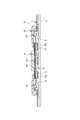
図11で示すポインティングデバイス1は、携帯電話機などの電子機器の筐体Cの透孔Chに露呈するキートップ2、磁石3、ベースシート4、プリント基板Pに実装したホール素子などの磁気センサ5を備えて構成される。ここで、ベースシート4は、キートップ2と磁石3とが固着され、これらを支持する厚肉の支持部4aと、薄肉の可撓部4bと、プリント基板Pに対する固定部4cと、が形成されている。そして、図11(A)から図11(B)で示すように、キートップ2を図中左に向けて側方移動させる操作を加えると、可撓部4bの伸縮変形によって、支持部4aとともに磁石3が側方移動し、これによる磁束密度の変化が磁気センサ5で検出されることになる。 A pointing device 1 shown in FIG. 11 includes a
ところが、この例のように、磁気センサ5がプリント基板Pの表面であっても、ベースシート4の支持部4aの下側にあると、図11(B)への側方移動時に、支持部4aが磁気センサ5と摺動接触することがあり、このため支持部4aに破断が生じたり、支持部4aとの摺動接触によりプリント基板Pに対する磁気センサ5の取付け状態が悪くなるおそれがある。したがって、支持部4aとプリント基板Pの表面との隙間を大きく設定しなければならず、このためポインティングデバイス1の薄型化に限界があり、電子機器に対する小型化の要請も満たすことができないという問題がある。 However, as in this example, even if the
以上のような従来技術を背景になされたのが本発明である。その目的は、プリント基板の表面に磁気センサを取付けても、ポインティングデバイスを薄型化できるようにすることにある。 The present invention has been made against the background of the prior art as described above. The purpose is to make the pointing device thinner even if a magnetic sensor is attached to the surface of the printed circuit board.
そこで、上記目的を達成すべく本発明は、磁石の支持部を側方移動できるように該移動方向で伸縮変形可能な可撓部を有するゴム状弾性体でなるベースシートを備えており、該支持部とともに側方移動する磁石による磁束密度の変化がプリント基板に設けた磁気センサで検出されるポインティングデバイス用のキーシートについて、ベースシートの可撓部に、該可撓部の裏面を、支持部の側方移動とともにプリント基板の表面から離間する方向へ誘導変位させる指向性変形部を形成したことを特徴とする。 Therefore, in order to achieve the above object, the present invention includes a base sheet made of a rubber-like elastic body having a flexible portion that can be expanded and contracted in the moving direction so that the support portion of the magnet can be moved sideways. For a key sheet for a pointing device in which a change in magnetic flux density due to a magnet moving laterally with the support portion is detected by a magnetic sensor provided on the printed circuit board, the back surface of the flexible portion is supported on the flexible portion of the base sheet. A directional deformation portion is formed that is guided and displaced in a direction away from the surface of the printed circuit board along with the lateral movement of the portion.
本発明では、支持部が側方移動すると、指向性変形部の変形によって、可撓部の裏面がプリント基板の表面から離間する方向へ誘導するように変位する。つまり、可撓部の裏面とプリント基板の表面との隙間が拡大する。このため、プリント基板の表面に磁気センサを取付けるとしても、支持部の下側に取付ける必要が無い点で、前述の従来例における薄型化の限界を克服して、まずポインティングデバイスの薄型化が達成される。また、可撓部の下側に磁気センサを取付けても、前記のように、可撓部が縮まる側方移動側では、指向性変形部によって隙間が拡大するため、可撓部が磁気センサとの摺動接触によっては破断しない。 In the present invention, when the support portion moves laterally, the back surface of the flexible portion is displaced so as to be guided away from the front surface of the printed circuit board due to the deformation of the directional deformation portion. That is, the gap between the back surface of the flexible part and the surface of the printed board is enlarged. For this reason, even if a magnetic sensor is attached to the surface of the printed circuit board, it is not necessary to attach it to the lower side of the support part. Is done. Even if the magnetic sensor is attached to the lower side of the flexible part, the gap is enlarged by the directional deformation part on the side moving side where the flexible part is contracted as described above. The sliding contact does not break.
このように、本発明のキーシートでは、可撓部が磁気センサとの摺動接触によっては破断しないものであるから、ベースシートを構成するゴム状弾性体の過剰な繰返しの伸縮変形に起因する劣化による破断までをも防止できるものではない。また、側方移動前の支持部の初期位置及び最大側方移動状態においては、可撓部が磁気センサと接触していてもよいものである。 As described above, in the key sheet of the present invention, the flexible portion is not broken by sliding contact with the magnetic sensor, and thus is caused by excessive repeated expansion and contraction of the rubber-like elastic body constituting the base sheet. It cannot prevent even the breakage due to deterioration. Moreover, in the initial position and maximum lateral movement state of the support part before the lateral movement, the flexible part may be in contact with the magnetic sensor.
また、前述の指向性変形部は、プリント基板の表面から離間する方向へ可撓部の裏面を誘導変位させるものであり、その一具体例として、本発明では、指向性変形部を、プリント基板の表面から離間する方向へ突出する山折り屈曲部として形成した。他の具体例としては、プリント基板の表面から離間する方向への屈曲が誘導されるように、指向性変形部をプリント基板との対向面側に下向き開口の凹溝を形成したものとして構成することもできる。 Further, the directional deformation portion described above is for inductively displacing the back surface of the flexible portion in a direction away from the front surface of the printed circuit board. As one specific example, in the present invention, the directional deformation portion is connected to the printed circuit board. It was formed as a mountain fold bent portion that protrudes in a direction away from the surface. As another specific example, the directional deformation portion is configured as a groove having a downward opening on the side facing the printed circuit board so that bending in a direction away from the surface of the printed circuit board is induced. You can also.
前記本発明の可撓部は、少なくとも裏面を、支持部側よりも指向性変形部側にかけて上向き傾斜面として形成したものとして構成できる。このため、支持部の側方移動時における可撓部と磁気センサの摺動接触を確実に回避できる。 The flexible part of the present invention can be configured such that at least the back surface is formed as an upward inclined surface from the support part side to the directional deformation part side. For this reason, the sliding contact between the flexible portion and the magnetic sensor during the lateral movement of the support portion can be reliably avoided.
前記本発明の可撓部は、指向性変形部側よりも支持部側を厚肉に形成したものとして構成できる。このため、支持部側が厚肉であり変形しにくいため、指向性変形部を確実に変形させることができる。 The flexible part of the present invention can be configured such that the support part side is formed thicker than the directional deformation part side. For this reason, since the support part side is thick and is hard to deform | transform, a directional deformation | transformation part can be deform | transformed reliably.
前記本発明の磁石は、環状の磁石として、また環状位置に配置する複数の磁石でなるものとして構成し、この場合、磁石の着磁方向を内外方向として構成できる。磁石の着磁方向を内外方向、例えば環状磁石であれば内周側にS極、外周側にN極のように着磁したものであれば、磁石の厚み方向、例えば上側にS極、下側にN極のように着磁したものと比較して外部に漏れる磁束密度を小さくでき温度特性も改善する。さらにポインティングデバイスを薄型化できる。さらに、磁気センサの感磁方向をプリント基板に対して水平方向とすることにより、磁石の移動に対する磁束の変化を大きく感知することができる。 The magnet of the present invention is configured as an annular magnet or a plurality of magnets arranged in an annular position, and in this case, the magnetizing direction of the magnet can be configured as the inner and outer directions. If the magnet is magnetized in the inner and outer directions, for example, if it is an annular magnet, such as S pole on the inner circumference side and N pole on the outer circumference side, the magnet thickness direction, eg, S pole on the upper side, lower The magnetic flux density leaking to the outside can be reduced as compared with the one magnetized like N pole on the side, and the temperature characteristics are also improved. Furthermore, the pointing device can be thinned. Furthermore, by making the magnetic sensor's magnetic sensing direction horizontal with respect to the printed circuit board, a change in magnetic flux with respect to the movement of the magnet can be greatly sensed.
前記本発明の磁石はプラスチックマグネットとして構成できる。これによれば、磁石の薄型化によるポインティングデバイスの薄型化が達成される。 The magnet of the present invention can be configured as a plastic magnet. According to this, it is possible to reduce the thickness of the pointing device by reducing the thickness of the magnet.
前記本発明については、支持部に磁石の収容凹部を形成し、支持部の表面に収容凹部を閉塞するキートップを取付けたものとして構成される。これによれば、キートップによって、収容凹部からの磁石の脱離を確実に防ぐことができる。また、キートップに磁石の収容凹部を形成することなく、ベースシートの支持部に磁石の収容凹部を形成することで、キートップの底面を平坦面にして、該底面に文字、数字、記号等の表示用の印刷層を形成することができるようになる。そして、支持部の表面に収容凹部を閉塞するキートップを取付ける具体的構成としては、支持部とキートップとの間に接着層を介在させて固着する構成とすることができる。この場合にはさらに、支持部だけでなく収容凹部内の磁石とキートップとの間にも接着層を介在させて固着する構成とすることが可能であり、これによればゴム状弾性体でなるベースシートの収容凹部が磁石の重量により垂れてしまうことを防ぐことができるようになる。 The present invention is configured such that a magnet receiving recess is formed in the support portion, and a key top for closing the receiving recess is attached to the surface of the support portion. According to this, the detachment of the magnet from the housing recess can be reliably prevented by the key top. In addition, by forming a magnet receiving recess in the support portion of the base sheet without forming a magnet receiving recess in the key top, the bottom surface of the key top is made flat, and letters, numbers, symbols, etc. are formed on the bottom surface. The display print layer can be formed. And as a concrete structure which attaches the key top which obstruct | occludes an accommodation recessed part on the surface of a support part, it can be set as the structure fixed by interposing an adhesive layer between a support part and a key top. In this case, it is further possible to adopt a configuration in which not only the support portion but also the magnet in the housing recess and the key top are fixed by interposing an adhesive layer. It becomes possible to prevent the housing concave portion of the base sheet from drooping due to the weight of the magnet.
前記本発明については、ベースシートを透光性のゴム状弾性体で形成するとともに、キートップを本体部と本体部の周囲に設けた鍔部とを有する透光性樹脂で形成し、磁石の収容凹部を支持部における該鍔部の対向位置に形成したものと構成できる。これによれば、照光用内部光源からの光が、透光性のベースシートと透光性樹脂でなるキートップの本体部とを透過できるため、照光機能が磁石によって阻害されず、照光式キーシートとして構成できる。With respect to the present invention, the base sheet is formed of a light-transmitting rubber-like elastic body, and the key top is formed of a light-transmitting resin having a main body portion and a collar portion providedaround the main body portion. The housing concave portion can be configured to be formed at a position of the support portion facing the flange portion. According to this, since the light from the illumination internal light source can pass through the translucent base sheet and the main body of the key top made of translucent resin, the illumination function is not hindered by the magnet, and the illuminated key Can be configured as a sheet.
前記本発明については、支持部を、透孔を有する薄肉支持部として形成するとともに、該透孔を通じて固着して支持部を表裏で狭持する上部キートップと硬質樹脂でなる下部キートップとを備えており、該下部キートップに磁石の収容凹部を形成したものと構成できる。磁石の収容凹部を下部キートップに形成することで、プリント基板の表面と対向する部位が、ゴム状弾性体でなるベースシートの支持部ではなく硬質樹脂でなる下部キートップとなるため、支持部の摩耗や破断による磁石の脱離を皆無にできる。 For the present invention, the support part is formed as a thin support part having a through hole, and an upper key top fixed through the through hole and holding the support part between the front and back and a lower key top made of hard resin are provided. It can comprise, and the accommodation recessed part of a magnet was formed in this lower key top. By forming the magnet receiving recess in the lower key top, the part facing the surface of the printed circuit board becomes the lower key top made of hard resin instead of the support part of the base sheet made of rubber-like elastic body. The magnet can be eliminated without any wear or breakage.
また、上記目的を達成すべく本発明は、ポインティングデバイスとしても構成される。すなわち、本発明は、磁石と、磁石の支持部を側方移動できるように該移動方向で伸縮変形可能な可撓部を有するゴム状弾性体でなるベースシートと、該支持部とともに側方移動する磁石による磁束密度の変化を検出するプリント基板に設けた磁気センサと、を備えるポインティングデバイスについて、ベースシートの可撓部に、該可撓部の裏面を、支持部の側方移動とともにプリント基板の表面から離間する方向へ誘導変位させる指向性変形部を形成したことを特徴とする。 In order to achieve the above object, the present invention is also configured as a pointing device. That is, the present invention provides a magnet, a base sheet made of a rubber-like elastic body having a flexible portion that can be expanded and contracted in the moving direction so that the support portion of the magnet can be moved laterally, and the side portion moves together with the support portion A pointing device including a magnetic sensor provided on a printed circuit board for detecting a change in magnetic flux density due to a magnet that performs a printed circuit board with the flexible part of the base sheet and the back surface of the flexible part along with the lateral movement of the support part A directional deformation portion is formed that is inductively displaced in a direction away from the surface of the substrate.
本発明によれば、ベースシートの可撓部における指向性変形部の変形によって、可撓部の裏面とプリント基板の表面との隙間が拡大するため、プリント基板の表面に磁気センサを取付けるとしても、支持部の下側に取付ける必要が無く、ポインティングデバイスの薄型化が達成され、また可撓部の下側に磁気センサを取付けても、可撓部が縮まる側方移動側での隙間の拡大により、可撓部が磁気センサとの摺動接触によっては破断しない。 According to the present invention, since the gap between the back surface of the flexible portion and the front surface of the printed circuit board is enlarged due to the deformation of the directional deformation portion in the flexible portion of the base sheet, the magnetic sensor may be attached to the front surface of the printed circuit board. There is no need to attach the support unit to the lower side, the pointing device can be made thinner, and even if a magnetic sensor is attached to the lower side of the flexible part, the flexible part shrinks and the gap on the side movement side is enlarged. Therefore, the flexible portion is not broken by sliding contact with the magnetic sensor.
前記本発明については、磁気センサを、プリント基板の表面における指向性変形部との対向位置に備えるものとして構成される。これによれば、支持部の下側ではなく、可撓部の下側に磁気センサが位置し、且つその上方には指向性変形部が対向するため、磁気センサをプリント基板の表面に実装しながらも、ベースシートが摺動接触により破断することなく、ポインティングデバイスの薄型化が達成される。 About the said invention, it comprises as a thing provided with a magnetic sensor in the position facing the directivity deformation part in the surface of a printed circuit board. According to this, the magnetic sensor is located on the lower side of the flexible part, not on the lower side of the support part, and the directional deformation part is opposed to the upper side. Therefore, the magnetic sensor is mounted on the surface of the printed circuit board. However, the pointing device can be made thinner without breaking the base sheet due to sliding contact.
前記本発明については、照光用内部光源を、プリント基板の表面における指向性変形部との対向位置に備えるものとして構成される。これによれば、支持部の下側ではなく、可撓部の下側に照光用内部光源が位置し、且つその上方には指向性変形部が対向するため、照光用内部光源をプリント基板の表面に実装しながらも、ベースシートが摺動接触により破断することなく、ポインティングデバイスの薄型化が達成され、且つ、照光機能を持たせることができる。 The present invention is configured such that the illumination internal light source is provided at a position facing the directional deformation portion on the surface of the printed board. According to this, since the illumination internal light source is located below the flexible portion, not below the support portion, and the directional deformation portion faces above, the illumination internal light source is disposed on the printed circuit board. While mounting on the surface, the base sheet is not broken by sliding contact, so that the pointing device can be made thinner and can have an illumination function.
前記本発明によるポインティングデバイスの各部の構成、すなわちベースシート、ベースシートの支持部、磁石、キートップについては、前述の本発明によるポインティングデバイス用のキーシートと構成をも備えることで、それらと同様の作用・効果を奏することができる。 The configuration of each part of the pointing device according to the present invention, that is, the base sheet, the support portion of the base sheet, the magnet, and the key top are also provided with the key sheet and configuration for the pointing device according to the present invention described above. The effects and effects of can be achieved.
本発明のポインティングデバイス用のキーシート及びポインティングデバイスによれば、キーシートにおけるベースシートの可撓部に指向性変形部を形成したことで、ポインティングデバイスを全体的に薄型化できるので、小型化・薄型化の要請が高い携帯電話機、PDA等の携帯機器についてもポインティングデバイスを搭載でき、表示画面のスクロールや座標入力など、多様な入力操作を実現できる。 According to the key sheet and the pointing device for the pointing device of the present invention, since the directional deformation portion is formed in the flexible portion of the base sheet in the key sheet, the pointing device can be thinned as a whole. A portable device such as a mobile phone and a PDA that are highly demanded to be thin can be equipped with a pointing device, and various input operations such as display screen scrolling and coordinate input can be realized.
以下、本発明の実施形態について図面を参照しつつ説明する。 Embodiments of the present invention will be described below with reference to the drawings.
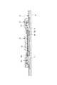
第1実施形態〔図1〜図3〕: 本実施形態のポインティングデバイス10は、中央キートップ11、外周キートップ12、ベースシート13、環状磁石14、プリント基板Pに実装した磁気センサ5にて構成される。なお、キーシートは、磁気センサ5を除く残余の構成によって構成される。First Embodiment [FIGS. 1 to 3] : A pointing
中央キートップ11は、エラストマーを含む硬質樹脂、金属などで形成されており、円柱状の本体部11aと円環状の鍔部11bが形成されている。外周キートップ12も、エラストマーを含む硬質樹脂、金属などによって、中央キートップ11を露出させる透孔12aを有する円環状に形成されている。中央キートップ11は、この透孔12aの差し渡し幅の範囲内で、360°全方向に移動可能となっている。 The central key top 11 is formed of a hard resin containing elastomer, metal, or the like, and is formed with a cylindrical
中央キートップ11は接着層15を介してベースシート13に固着されており、同じく外周キートップ12も図外の接着層を介してベースシート13に固着されている。ベースシート13は、中央キートップ11と環状磁石14を支持する厚肉円柱状の支持部13aと、支持部13aの外周を包囲する可撓部13bとが形成されている。 The central key top 11 is fixed to the
支持部13aの中央には押し子13cが形成されており、したがって中央キートップ11を押圧操作すれば、押し子13cによってプリント基板Pの接点皿ばねPiが座屈して、スイッチ入力が可能となっている。また、支持部13aには、環状磁石14の収容凹部13dが形成される。したがって、この収容凹部13dは、中央キートップ11の鍔部11bによって接着層15を介して封止されており、よって環状磁石14が脱離しないようになっている。A
可撓部13bは、内周側から順に上向きの傾斜面部13e、波状のベローズ部13f、平坦部13gにて構成される。 The
上向きの傾斜面部13eは、支持部13aに対する付け根側が厚肉に形成されており、外側に広がるにつれて薄肉に形成されている。このため相対的に、厚肉の付け根側では変形しにくく、外側に広がるにつれて変形しやくなっている。また、傾斜面部13eは、付け根側から外側に広がるにつれて上向きに傾斜しており、プリント基板Pとの間隔が拡大されている。したがって、図1の状態で、磁気センサ5から離間している。 The upward
ベローズ部13fは、傾斜面部13eの外周上端から外側へ多段に屈曲形成されており、この多段の屈曲によって、中央キートップ11を側方移動に併せて伸縮可能となっている。側方移動させた中央キートップ11の初期位置への復帰力は、主としてこのベローズ部13fによって付与される。 The
平坦部13gは、ベローズ部13fの下端から水平方向に形成されている。この平坦部13gにも押し子13hが形成されており、外周キートップ12を押圧操作すれば、押し子13hが接点皿ばねPoを座屈させ、スイッチ入力が可能となっている。 The
環状磁石14は、本実施形態のものはアルニコ磁石、フェライト磁石、サマリウム−コバルト磁石、ネオジウム磁石などの粉体をバインダー樹脂に充填して金型成形してなるプラスチックマグネットを利用している。したがって、環状磁石14は薄型であり、ポインティングデバイス10の全体の薄型化に寄与している。また、環状磁石14は、図2で示すように、外周側部分がN極に、内周側部分がS極に着磁されている。このように着磁方向が内外方向であるため、着磁方向が厚み方向である場合と比較して、外部に漏れる磁束密度を小さくできる。また、着磁方向が側方移動させる中央キートップ11の移動方向とも合致するため、磁気センサ5における磁束密度の検出精度も高めることができるようになっている。さらに、環状磁石14の高温域での磁気特性を安定化できる。 In the present embodiment, the
磁気センサ5は、具体的にはホール素子、ホールIC、磁気抵抗効果素子、磁気抵抗効果ICなどを利用できる。本実施形態における配置は、図2で示すように、上下左右の各位置に配置した接点皿ばねPoの内側位置である。 Specifically, the
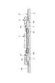
次に、以上のポインティングデバイス10の作用・効果を説明する。 Next, the operation and effect of the
ベースシート11の可撓部13bには、前述のとおり、上向きの傾斜面部13eとベローズ部13fとが形成され、この双方を繋ぐ部分が、プリント基板Pの表面から離間する方向へ突出する「指向性変形部」としての山折り屈曲部13iとして機能する。すなわち、図3(A)で示すように、中央キートップ11を図中左へ側方移動させると、支持部13aの側方移動に伴って可撓部13bも移動するが、このとき可撓部13bは、図3(B)で示すように、山折り屈曲部13iにおける斜め上方への変形をきっかけとして、可撓部13bをプリント基板Pの表面から離間する方向へ誘導変位される。したがって、支持部13aの下側におけるプリント基板Pの表面に磁気センサ5を取付けない点で、ポインティングデバイス10を薄型化可能であり、また可撓部13bの下側に磁気センサ5を取付けても、可撓部13bとプリント基板Pとの隙間が拡大され、可撓部13bが磁気センサ5に対して摺動接触することを防止でき、摺動接触による破断を阻止できる。この結果、小型化・薄型化の要請が高い携帯電話機、PDA等の携帯機器についてもポインティングデバイス10を搭載でき、表示画面のスクロールや座標入力など、多様な入力操作を実現できる。 As described above, the
なお、図3で示す縮み変形する側とは反対の伸び変形する側では、ベローズ部13fの下端と磁気センサ5との間に予め隙間が設定されているため、伸び変形したベローズ部13fと磁気センサ5との接触を避けることができる。 In addition, since the gap is set in advance between the lower end of the
上記のように変形する可撓部13bの傾斜面部13eは、支持部13aに対する厚肉の付け根側では変形しにくく、外側に広がるにつれて変形しやい。したがって、中央キートップ11を側方移動させることで、傾斜面部13eが付け根側から意図せず座屈するように変形することがなく、可撓部13bに対する誘導変位を確実に行うことができる。また、側方移動により伸び変形する側で傾斜面部13eが伸びても、厚肉の付け根側が変形しにくく傾斜状態が維持されて、傾斜面部13eとベローズ部13fの磁気センサ5への接近を小さくできるため、これによっても磁気センサ5との接触を回避できる。 The
第2実施形態〔図4,図5〕: 本実施形態は、中央キートップ11に照光機能を実現する構成を付加した点が、第1実施形態によるポインティングデバイス10と相違している。Second Embodiment [FIGS. 4 and 5] : This embodiment is different from the
具体的な相違点は、第1に、中央キートップ11が透明な硬質樹脂で形成したことである。第2に、接着層15を透光性接着剤にて形成したことである。第3に、ベースシート12を、透光性のゴム状弾性体にて形成したことである。第4に、中央キートップ11の底面に、文字、数字、記号等の象る抜き文字印刷層11cと、抜き文字印刷層11cの抜き文字部分を充填する白色・金属色を含む着色層11dを形成したことである。第5として、図5で示すように、LEDなどの照光用の内部光源16をプリント基板Pに備えるようにしたことである。さらに、第6として、図5で示すように、第1実施形態の環状磁石14とは異なり、各磁気センサ5との対向位置に複数の磁石片17を備える構成とし、ベースシート13には各磁石片17に対応する周方向で分断した収容凹部13kを形成したことである。 A specific difference is that, first, the central key top 11 is formed of a transparent hard resin. Second, the
第1実施形態のポインティングデバイス10に、前記構成を付加することによって、第1実施形態で説明した作用・効果に加えて、内部光源16からの光を、ベースシート13、接着層15、着色層11d、抜き文字印刷層11c、中央キートップ11を通じて照光することができる。 By adding the above configuration to the
この場合に、磁石片17は、第1実施形態のような無端の環状磁石14ではなく分断しているため、図5で矢示するように、ベースシート13における磁石片17どうし隣接部分を光路にできるため、明るく照光することができる。 In this case, since the
さらに、内部光源16は、磁気センサ5と同じ周上位置に配置しているので、中央キートップ11の側方移動時に、可撓部13bが内部光源16との摺動接触により破断することはない。Furthermore, since the internal
第3実施形態〔図6〕: 本実施形態は、中央キートップ18の構成が、第1実施形態のポインティングデバイス10と異なり、残余の構成は同一である。すなわち、本実施形態の中央キートップ18は、樹脂フィルム18aに硬質樹脂でなる本体部18bを一体成形したものである。したがって、このようなフィルム一体型キートップとした中央キートップ18による利点は、樹脂フィルム18aによる鍔部18cの厚みを0.3mm以下とすることができ、更なる薄型化を図ることができることである。しかも、薄型化しても、鍔部18cが破損するような不都合が無い。Third Embodiment [FIG. 6] : In this embodiment, the configuration of the central key top 18 is different from the
第4実施形態〔図7〕: 本実施形態は、中央キートップ19の鍔部19aに環状磁石14を一体成形したことが、第1実施形態のポインティングデバイス10と異なる。この構成によれば、中央キートップ19と環状磁石14とが一つの成形体であることから、ベースシート13への接着工程時に、環状磁石14を位置決め突起として機能させて収容凹部13dに収容することで位置決め精度を高めることができる。また、鍔部19aの肉厚分だけ更なる薄型化に寄与することができる。Fourth Embodiment [FIG. 7] : This embodiment is different from the
第5実施形態〔図8〕: 本実施形態は、中央キートップ20と、ベースシート21が第1実施形態のポインティングデバイス10と異なる。Fifth Embodiment [FIG. 8] : In this embodiment, the central key top 20 and the
すなわち、本実施形態のベースシート21は、支持部21aが透孔21bを有する薄肉に形成されており、可撓部21cにおける傾斜面部21dが薄肉等厚で形成されている。また、本実施形態の中央キートップ20は、薄肉の支持部21aを表裏から狭持する何れも硬質樹脂でなる上部キートップ20aと下部キートップ20bで構成されており、このうち下部キートップ20bに環状磁石14の収容凹部20cを形成したものである。 That is, in the
この構成によれば、第1実施形態と同様の作用・効果に加えて、プリント基板Pとの対向部分が、例えば第1実施形態のようにゴム状弾性体でなるベースシート13ではなく、硬質樹脂でなる下部キートップ20bである。このため、中央キートップ20の側方移動時にプリント基板Pと摺動接触しても、破断により環状磁石14が脱離する不都合を皆無にできる。また、中央キートップ20の側方移動時には、ゴム状弾性体よりも摩擦係数の小さい硬質樹脂でなる下部キートップ20bの押し子20dが、金属製の接点皿ばねPiと摺動接触するため、スムーズな側方移動を行える利点もある。 According to this configuration, in addition to the same operations and effects as in the first embodiment, the portion facing the printed circuit board P is not the
第6実施形態〔図9〕: 本実施形態は、ベースシート22の構成が、第1実施形態のベースシート13と異なる。すなわち、ベースシート22の可撓部22aは、断面V字状のV形屈曲部22bと、内側平坦部22cと、外側平坦部22dで構成される。そして、本実施形態では、V形屈曲部22bと内側平坦部22cとが連続する境界部22eが、「指向性変形部」として機能するものである。具体的には、中央キートップ11を側方移動させると、支持部22fにより付勢されて、V形屈曲部22bが潰れるように変形していき、その過程で、境界部22eが上方に変形することで、可撓部22aの裏面がプリント基板Pの表面から離れる方向へ誘導変位される。これによっても、第1実施形態の山折り屈曲部13iと同様の作用・効果を達成できる。6th Embodiment [FIG. 9] : This embodiment differs in the structure of the
各実施形態の細部変形例: 以上の実施形態については、例えばベースシート13に中央キートップ11や外周キートップ12に相当する操作用突起を形成してもよい。Detailed Modification of Each Embodiment : In the above embodiment, for example, operation protrusions corresponding to the central key top 11 and the outer peripheral key top 12 may be formed on the
以上の実施形態では、外周キートップ12を周方向で分割して構成してもよい。また、外周キートップ12を設けず、中央キートップ11のみを有するポインティングデバイスとして構成することもできる。この場合、操作方向は360度全方向への又は特定方向への入力操作を可能なものとして構成し、それに応じて磁気センサ5の数や配置を変更してもよい。 In the above embodiment, the outer peripheral key top 12 may be divided in the circumferential direction. Moreover, it is also possible to configure as a pointing device having only the central key top 11 without providing the outer peripheral
以上の実施形態では、各実施形態に特有の構成をその他の実施形態に適用することも可能である。例えば、第2実施形態の抜き文字印刷層11cや着色層11dを他の実施形態に適用してもよい。なお、抜き文字印刷層11cではなく、文字印刷層と着色層としてもよい。 In the above embodiment, the configuration unique to each embodiment can be applied to other embodiments. For example, the blank character printed
以上の実施形態では、例えばベースシート13を構成するゴム状弾性体として、シリコーンゴム等の熱硬化性エラストマーやスチレン系等の熱可塑性エラストマーを使用できる。また、例えば、ベースシート13として熱可塑性エラストマーを選択し、中央キートップ11として熱可塑性樹脂を選択すれば、二色成形により一体成形が可能であり、接着工程が不要で、固着力も強固にできる。 In the above embodiment, for example, as the rubber-like elastic body constituting the
以上の実施形態では、例えば環状磁石14をプラスチックマグネットにて形成した例を示したが、やや厚みが出ても構わなければ、それ以外の磁石であってもよい。 In the above embodiment, for example, the
以上の実施形態では、磁気センサ5を接点皿ばねPiと接点皿ばねPoとの間に配置する例を示したが、例えば、図2においては、接点皿ばねPiを中心に45度ずらした位置に、磁気センサ5を配置することで、接点皿ばねPoの間に磁気センサ5を配置することができ、より小型化が可能となる。また、図5においては、磁気センサ5と内部光源16とを接点皿ばねPiを中心に30度ずらして、磁気センサ5と内部光源16とを、接点皿ばねPoの間に配置することもできる。この場合、磁石17は磁気センサ5と対向する位置に配置すればよい。 In the above embodiment, the example in which the
第1〜第4、第6の各実施形態では、押し子(図1の符号13c)を全体としてゴム状弾性体にて形成する例を示したが、側方移動をより円滑に行えるように、図10のように構成することができる。図10(A)は、押し子23に硬質樹脂でなる先端部23aを設けた例であり、図10(B)は、硬質樹脂でなる押し子24をベースシートの裏面に設けた例である。これらによれば、前述の各実施形態におけるゴム状弾性体でなる押し子よりも耐摩耗性が高く、摺動摩擦による引っ掛かりを少なくできるため、スムーズな側方移動が行える。そして、これらに加えて図10の各例では、金属製の接点皿ばねPiを覆うように、樹脂フィルムPfを貼着や接着にて固着してある。この樹脂フィルムPfとしては、耐摩耗性があり低摩擦係数に優れるフッ素樹脂、ポリアミド樹脂等からなる樹脂フィルムを利用することができる。接点皿ばねPiにこうした樹脂フィルムPfを取付けることで、摺動摩擦による引っ掛かりがさらに低減されて、よりスムーズな側方移動を確実に行うことが可能である。なお、耐摩耗性の向上と摺動摩擦の低減という点で、図10で示す構成が最も好ましいが、先端部23aや押し子24を形成するか、または樹脂フィルムPfを取付けるか、の何れか一方として構成することも可能である。 In each of the first to fourth and sixth embodiments, the example in which the pusher (reference numeral 13c in FIG. 1) is formed of a rubber-like elastic body as a whole has been shown, but the lateral movement can be performed more smoothly. 10 can be configured as shown in FIG. FIG. 10A is an example in which a
第2実施形態では、中央キートップ11だけに照光機能を実現する例を示したが、外周キートップ12を透光性樹脂で形成し、内部光源16により照光する照光機能を備える構成としてもよい。In the second embodiment, an example in which the illumination function is realized only in the central key top 11 has been described. However, the outer peripheral key top 12 may be formed of a translucent resin and may have an illumination function of illuminating with the internal
第3実施形態では、中央キートップ18として、本体部18bの上面及び側面に対し樹脂フィルム18aを一体形成する例を示したが、本体部18bの底面に対し、鍔部の分だけ広い樹脂フィルムを一体形成する構成としてもよい。 In the third embodiment, an example in which the
5 磁気センサ
10 ポインティングデバイス
11 中央キートップ
11a 本体部
11b 鍔部
11c 抜き文字印刷層
11d 着色層
12 外周キートップ
12a 透孔
13 ベースシート
13a 支持部
13b 可撓部
13c 押し子
13d 収容凹部
13e 傾斜面部
13f ベローズ部
13g 平坦部
13h 押し子
13i 山折り屈曲部(指向性変形部)
13k 収容凹部
14 環状磁石(磁石)
15 接着層
16 内部光源
17 磁石片(磁石)
18 中央キートップ
18a 樹脂フィルム
18b 本体部
18c 鍔部
19 中央キートップ
19a 鍔部
20 中央キートップ
20a 上部キートップ
20b 下部キートップ
20c 収容凹部
21 ベースシート
21a 支持部
21b 透孔
21c 可撓部
22 ベースシート
22a 可撓部
22b 屈曲部
22c 内側平坦部
22d 外側平坦部
22e 境界部(指向性変形部)
23 押し子
23a 先端部
24 押し子5
15
18 Central key top
23
Claims (18)
Translated fromJapaneseベースシートの可撓部に、該可撓部の裏面を、支持部の側方移動とともにプリント基板の表面から離間する方向へ誘導変位させる指向性変形部を形成し、
磁石を、環状の磁石又は環状位置に配置する複数の磁石でなるものとして構成して磁石の着磁方向を内外方向としたことを特徴とするポインティングデバイス用のキーシート。A base sheet made of a rubber-like elastic body having a flexible part that can be expanded and contracted in the moving direction is provided so that the support part of the magnet can be moved sideways. In a key sheet for a pointing device in which a change is detected by a magnetic sensor provided on a printed circuit board,
On the flexible part of the base sheet, a directional deformation part is formed that inductively displaces the back surface of the flexible part in a direction away from the surface of the printed circuit board along with the lateral movement of the support part.
A key sheet for a pointing device, characterizedin that the magnet is composed of an annular magnet or a plurality of magnets arranged in an annular position, and the magnetizing direction of the magnet is set to the inner and outer directions .
ベースシートの可撓部に、該可撓部の裏面を、支持部の側方移動とともにプリント基板の表面から離間する方向へ誘導変位させる指向性変形部を形成し、
支持部に磁石の収容凹部を形成し、支持部の表面に収容凹部を閉塞するキートップを取付け、
ベースシートを透光性のゴム状弾性体で形成するとともに、キートップを本体部と本体部の周囲に設けた鍔部とを有する透光性樹脂で形成し、磁石の収容凹部を支持部における該鍔部の対向位置に形成したことを特徴とするポインティングデバイス用のキーシート。A base sheet made of a rubber-like elastic body having a flexible part that can be expanded and contracted in the moving direction is provided so that the support part of the magnet can be moved sideways. In a key sheet for a pointing device in which a change is detected by a magnetic sensor provided on a printed circuit board,
A directional deformation part is formed on the flexible part of the base sheet to induce and displace the back surface of the flexible part in a direction away from the surface of the printed circuit board along with the lateral movement of the support part.
A magnet receiving recess is formed in the support, and a key top for closing the receiving recess is attached to the surface of the support.
The base sheet is formed of a translucent rubber-like elastic body, the key top is formed of a translucent resin having a main body portion and a flange provided around the main body portion, and the magnet housing recess is formed in the support portion.A key sheet for a pointing device, whereinthe key sheetis formed at a position opposite to the collar .
ベースシートの可撓部に、該可撓部の裏面を、支持部の側方移動とともにプリント基板の表面から離間する方向へ誘導変位させる指向性変形部を形成し、
支持部を、透孔を有する薄肉支持部として形成するとともに、該透孔を通じて固着して支持部を表裏で狭持する上部キートップと下部キートップとを備えており、該下部キートップに磁石の収容凹部を形成したことを特徴とするポインティングデバイス用のキーシート。A base sheet made of a rubber-like elastic body having a flexible part that can be expanded and contracted in the moving direction is provided so that the support part of the magnet can be moved sideways. In a key sheet for a pointing device in which a change is detected by a magnetic sensor provided on a printed circuit board,
On the flexible part of the base sheet, a directional deformation part is formed that inductively displaces the back surface of the flexible part in a direction away from the surface of the printed circuit board along with the lateral movement of the support part.
The support portion is formed as a thin support portion having a through hole, and includes an upper key top and a lower key top that are fixed through the through hole and sandwich the support portion between the front and back sides, and a magnet is provided on the lower key top. key sheetfor a pointing device, characterized inthat the recess of the housing formation.
ベースシートの可撓部に、該可撓部の裏面を、支持部の側方移動とともにプリント基板の表面から離間する方向へ誘導変位させる指向性変形部を形成し、
磁気センサを、プリント基板の表面における可撓部との対向位置に備え、磁石をその側方移動方向で磁気センサと重なる位置に備えることを特徴とするポインティングデバイス。Magnetic flux density by a magnet, a base sheet made of a rubber-like elastic body having a flexible portion that can be expanded and contracted in the moving direction so that the support portion of the magnet can be moved laterally, and a magnet that moves sideways with the support portion In a pointing device comprising a magnetic sensor provided on a printed circuit board for detecting a change,
On the flexible part of the base sheet, a directional deformation part is formed that inductively displaces the back surface of the flexible part in a direction away from the surface of the printed circuit board along with the lateral movement of the support part.
A pointing device comprising: amagnetic sensor at a position facing a flexible portion on a surface of a printed circuit board; and a magnet provided at a position overlapping with the magnetic sensor in a lateral movement direction thereof .
ベースシートの可撓部に、該可撓部の裏面を、支持部の側方移動とともにプリント基板の表面から離間する方向へ誘導変位させる指向性変形部を形成し、
照光用内部光源を、プリント基板の表面における指向性変形部との対向位置に備えることを特徴とするポインティングデバイス。Magnetic flux density by a magnet, a base sheet made of a rubber-like elastic body having a flexible portion that can be expanded and contracted in the moving direction so that the support portion of the magnet can be moved laterally, and a magnet that moves sideways with the support portion In a pointing device comprising a magnetic sensor provided on a printed circuit board for detecting a change,
On the flexible part of the base sheet, a directional deformation part is formed that inductively displaces the back surface of the flexible part in a direction away from the surface of the printed circuit board along with the lateral movement of the support part.
A pointing device comprising anillumination internal light source at a position facing a directional deformation portion on a surface of a printed circuit board .
ベースシートの可撓部に、該可撓部の裏面を、支持部の側方移動とともにプリント基板の表面から離間する方向へ誘導変位させる指向性変形部を形成し、
磁石を、環状の磁石又は環状位置に配置する複数の磁石でなるものとして構成し、磁石の着磁方向を内外方向としたことを特徴とするポインティングデバイス。Magnetic flux density by a magnet, a base sheet made of a rubber-like elastic body having a flexible portion that can be expanded and contracted in the moving direction so that the support portion of the magnet can be moved laterally, and a magnet that moves sideways with the support portion In a pointing device comprising a magnetic sensor provided on a printed circuit board for detecting a change,
On the flexible part of the base sheet, a directional deformation part is formed that inductively displaces the back surface of the flexible part in a direction away from the surface of the printed circuit board along with the lateral movement of the support part.
A pointing device characterized inthat the magnet is composed of an annular magnet or a plurality of magnets arranged in an annular position, and the magnetizing direction of the magnet is the inside and outside direction .
ベースシートの可撓部に、該可撓部の裏面を、支持部の側方移動とともにプリント基板の表面から離間する方向へ誘導変位させる指向性変形部を形成し、
支持部に磁石の収容凹部を形成し、支持部の表面に収容凹部を閉塞するキートップを取付け、
ベースシートを透光性のゴム状弾性体で形成するとともに、キートップを本体部と本体部の周囲に設けた鍔部とを有する透光性樹脂で形成し、磁石の収容凹部を支持部における該鍔部の対向位置に形成したことを特徴とするポインティングデバイス。Magnetic flux density by a magnet, a base sheet made of a rubber-like elastic body having a flexible portion that can be expanded and contracted in the moving direction so that the support portion of the magnet can be moved laterally, and a magnet that moves sideways with the support portion In a pointing device comprising a magnetic sensor provided on a printed circuit board for detecting a change,
On the flexible part of the base sheet, a directional deformation part is formed that inductively displaces the back surface of the flexible part in a direction away from the surface of the printed circuit board along with the lateral movement of the support part.
A magnet receiving recess is formed in the support, and a key top for closing the receiving recess is attached to the surface of the support.
The base sheet is formed of a translucent rubber-like elastic body, the key top is formed of a translucent resin having a main body portion and a flange provided around the main body portion, and the magnet accommodating recess is formed in the support portion. A pointing device, characterized in that the pointing deviceis formed at a position opposite to the collar.
ベースシートの可撓部に、該可撓部の裏面を、支持部の側方移動とともにプリント基板の表面から離間する方向へ誘導変位させる指向性変形部を形成し、
支持部を、透孔を有する薄肉支持部として形成するとともに、該透孔を通じて固着して支持部を表裏で狭持する上部キートップと下部キートップとを備えており、該下部キートップに磁石の収容凹部を形成したことを特徴とするポインティングデバイス。Magnetic flux density by a magnet, a base sheet made of a rubber-like elastic body having a flexible portion that can be expanded and contracted in the moving direction so that the support portion of the magnet can be moved laterally, and a magnet that moves sideways with the support portion In a pointing device comprising a magnetic sensor provided on a printed circuit board for detecting a change,
On the flexible part of the base sheet, a directional deformation part is formed that inductively displaces the back surface of the flexible part in a direction away from the surface of the printed circuit board along with the lateral movement of the support part.
The support portion is formed as a thin support portion having a through hole, and includes an upper key top and a lower key top that are fixed through the through hole and sandwich the support portion between the front and back sides, and a magnet is provided on the lower key top. A pointing device characterized inthat an accommodation recess is formed .
Priority Applications (5)
| Application Number | Priority Date | Filing Date | Title |
|---|---|---|---|
| JP2004163736AJP4495525B2 (en) | 2004-06-01 | 2004-06-01 | Key sheet for pointing device and pointing device |
| EP05011431AEP1607849A3 (en) | 2004-06-01 | 2005-05-27 | Key sheet for pointing device and pointing device |
| US11/138,436US7508376B2 (en) | 2004-06-01 | 2005-05-27 | Key sheet for pointing device and pointing device |
| CNB2005100743128ACN100378890C (en) | 2004-06-01 | 2005-05-31 | Key sheet for pointing device and pointing device |
| KR1020050046879AKR101118069B1 (en) | 2004-06-01 | 2005-06-01 | Key sheet for pointing device and pointing device |
Applications Claiming Priority (1)
| Application Number | Priority Date | Filing Date | Title |
|---|---|---|---|
| JP2004163736AJP4495525B2 (en) | 2004-06-01 | 2004-06-01 | Key sheet for pointing device and pointing device |
Publications (2)
| Publication Number | Publication Date |
|---|---|
| JP2005347042A JP2005347042A (en) | 2005-12-15 |
| JP4495525B2true JP4495525B2 (en) | 2010-07-07 |
Family
ID=35116132
Family Applications (1)
| Application Number | Title | Priority Date | Filing Date |
|---|---|---|---|
| JP2004163736AExpired - Fee RelatedJP4495525B2 (en) | 2004-06-01 | 2004-06-01 | Key sheet for pointing device and pointing device |
Country Status (5)
| Country | Link |
|---|---|
| US (1) | US7508376B2 (en) |
| EP (1) | EP1607849A3 (en) |
| JP (1) | JP4495525B2 (en) |
| KR (1) | KR101118069B1 (en) |
| CN (1) | CN100378890C (en) |
Families Citing this family (36)
| Publication number | Priority date | Publication date | Assignee | Title |
|---|---|---|---|---|
| JP4561394B2 (en)* | 2005-02-17 | 2010-10-13 | オムロン株式会社 | Operation input device and electronic apparatus using the same |
| JP4584782B2 (en)* | 2005-06-21 | 2010-11-24 | 旭化成エレクトロニクス株式会社 | Pointing device and key sheet for pointing device |
| KR100789725B1 (en)* | 2006-05-15 | 2008-01-02 | 삼성전기주식회사 | Input device |
| JP4605474B2 (en)* | 2006-06-06 | 2011-01-05 | サンアロー株式会社 | Multi-directional input device |
| KR100857166B1 (en)* | 2006-11-29 | 2008-09-05 | 삼성전기주식회사 | Input device and portable terminal having same |
| KR100783470B1 (en)* | 2006-11-29 | 2007-12-07 | 삼성전기주식회사 | Mobile devices |
| KR100783469B1 (en)* | 2006-11-29 | 2007-12-07 | 삼성전기주식회사 | Mobile devices |
| KR100862950B1 (en)* | 2007-02-14 | 2008-10-15 | 주식회사 이노칩테크놀로지 | Pointing device and portable terminal having same |
| TW200842666A (en)* | 2007-04-26 | 2008-11-01 | Distech Technology Co Ltd | Direction control device |
| JP2010533336A (en)* | 2007-07-11 | 2010-10-21 | ユイ・ジン・オ | Data input device using finger motion sensing and input conversion method using the same |
| WO2009063799A1 (en)* | 2007-11-12 | 2009-05-22 | Alps Electric Co., Ltd. | Input device |
| KR100931071B1 (en)* | 2008-04-14 | 2009-12-10 | 주식회사 이노칩테크놀로지 | How to activate an electronic device and its icon |
| JP5098928B2 (en)* | 2008-09-26 | 2012-12-12 | オムロン株式会社 | INPUT DEVICE AND ELECTRONIC DEVICE USING THE SAME |
| JP2010114010A (en)* | 2008-11-10 | 2010-05-20 | Shin Etsu Polymer Co Ltd | Lighting structure of mobile apparatus |
| TWM360436U (en)* | 2009-01-12 | 2009-07-01 | Speed Tech Corp | Structure of low profile multi-directional key |
| KR101022406B1 (en) | 2009-01-29 | 2011-03-15 | 주식회사 이노칩테크놀로지 | Pointing device and electronic device having the same |
| JP5267504B2 (en)* | 2009-05-19 | 2013-08-21 | ミツミ電機株式会社 | Operation input device and operation input detection device |
| JP5356165B2 (en)* | 2009-09-10 | 2013-12-04 | 信越ポリマー株式会社 | pointing device |
| JP2012138167A (en) | 2009-09-30 | 2012-07-19 | Nec Corp | Analog pointing key structure |
| CN102044371A (en)* | 2009-10-19 | 2011-05-04 | 英业达股份有限公司 | Direction control device |
| JP5440284B2 (en)* | 2010-03-12 | 2014-03-12 | 日本電気株式会社 | Analog pointing key structure |
| DE102010003292A1 (en)* | 2010-03-25 | 2011-09-29 | Fraunhofer-Gesellschaft zur Förderung der angewandten Forschung e.V. | Sensor arrangement and method for determining a magnetization device of a transmitter magnet |
| JP2012027786A (en)* | 2010-07-26 | 2012-02-09 | Omron Corp | Input device and electronic equipment |
| DE102010039558A1 (en)* | 2010-08-20 | 2012-02-23 | BSH Bosch und Siemens Hausgeräte GmbH | Operating device for a household appliance with a power supply device and household appliance for preparing food with such an operating device |
| CN103140821B (en)* | 2010-08-30 | 2016-02-10 | 日本电气株式会社 | Input media and the electronic equipment being configured with input media |
| KR20120049630A (en)* | 2010-11-09 | 2012-05-17 | 주식회사 이노칩테크놀로지 | Multi-direction input device |
| US9569002B2 (en) | 2010-12-17 | 2017-02-14 | Blackberry Limited | Portable electronic device having a sensor arrangement for gesture recognition |
| JP6096764B2 (en)* | 2011-06-02 | 2017-03-15 | ノニン・メディカル・インコーポレーテッド | Home uterine activity monitoring |
| CN103187195A (en)* | 2011-12-27 | 2013-07-03 | 名硕电脑(苏州)有限公司 | Magnetic separation key and keyboard |
| KR101584537B1 (en)* | 2014-06-23 | 2016-01-22 | 엘지전자 주식회사 | Key module and mobile terminal having the same |
| JP2015043344A (en)* | 2014-12-02 | 2015-03-05 | レノボ・イノベーションズ・リミテッド(香港) | Analog pointing key structure |
| JP6784518B2 (en)* | 2016-06-10 | 2020-11-11 | 株式会社ソニー・インタラクティブエンタテインメント | Operation device |
| US20180068145A1 (en)* | 2016-09-07 | 2018-03-08 | Hand Held Products, Inc. | Smart scan peripheral |
| TWI702626B (en)* | 2018-03-30 | 2020-08-21 | 英屬開曼群島商康而富控股股份有限公司 | Touch button with better pressing feel |
| JP6529017B1 (en)* | 2018-05-23 | 2019-06-12 | 株式会社オリンピア | Gaming machine |
| TWI815275B (en)* | 2022-01-13 | 2023-09-11 | 華碩電腦股份有限公司 | Portable electronic device |
Family Cites Families (24)
| Publication number | Priority date | Publication date | Assignee | Title |
|---|---|---|---|---|
| JPH07117876B2 (en)* | 1990-09-18 | 1995-12-18 | 富士通株式会社 | Pointing control device |
| JP2953775B2 (en) | 1990-11-07 | 1999-09-27 | 富士通株式会社 | Pointing control device |
| JPH0635599A (en) | 1992-07-14 | 1994-02-10 | Fujitsu Ltd | Pointing device |
| JPH06318134A (en)* | 1994-03-15 | 1994-11-15 | Les-Ben:Kk | Data input device |
| JPH07262879A (en)* | 1994-03-23 | 1995-10-13 | Aiwa Co Ltd | Slide switch |
| JPH08185257A (en) | 1994-10-31 | 1996-07-16 | Matsushita Electric Ind Co Ltd | Coordinate input device |
| JPH08152961A (en) | 1994-11-30 | 1996-06-11 | Fujitsu Ltd | pointing device |
| JPH0934644A (en) | 1995-07-21 | 1997-02-07 | Oki Electric Ind Co Ltd | Pointing device |
| JP3428255B2 (en) | 1995-10-30 | 2003-07-22 | シャープ株式会社 | Input device such as computer |
| US5714980A (en)* | 1995-10-31 | 1998-02-03 | Mitsumi Electric Co., Ltd. | Pointing device |
| JP2000235822A (en)* | 1999-02-15 | 2000-08-29 | Snk Corp | Multi-directional switch and portable electronic apparatus using the same |
| JP3828676B2 (en)* | 1999-03-23 | 2006-10-04 | ホシデン株式会社 | Pointing device |
| JP2001228967A (en)* | 2000-02-17 | 2001-08-24 | Polymatech Co Ltd | Pointing device |
| GB2367346B (en)* | 2000-09-28 | 2004-07-14 | Nokia Mobile Phones Ltd | Control device |
| JP4121730B2 (en)* | 2001-01-19 | 2008-07-23 | 富士通コンポーネント株式会社 | Pointing device and portable information device |
| ATE419576T1 (en) | 2001-04-19 | 2009-01-15 | Asahi Kasei Emd Corp | DISPLAY DEVICE |
| JP4100897B2 (en)* | 2001-11-28 | 2008-06-11 | 松下電器産業株式会社 | Multi-directional operation switch and manufacturing method thereof |
| JP4105432B2 (en)* | 2001-12-21 | 2008-06-25 | アルプス電気株式会社 | Multi-directional input device |
| DE10212929A1 (en)* | 2002-03-19 | 2003-10-02 | Ego Elektro Geraetebau Gmbh | Control device for an electrical device |
| JP4175007B2 (en)* | 2002-03-22 | 2008-11-05 | 松下電器産業株式会社 | Rotation operation type input device |
| JP4147839B2 (en)* | 2002-06-26 | 2008-09-10 | ポリマテック株式会社 | Sliding multi-directional input key |
| JP4108401B2 (en)* | 2002-07-26 | 2008-06-25 | 日本電気株式会社 | Input device and mobile terminal |
| JP4612361B2 (en)* | 2004-08-31 | 2011-01-12 | ポリマテック株式会社 | Key switch |
| JP4584782B2 (en)* | 2005-06-21 | 2010-11-24 | 旭化成エレクトロニクス株式会社 | Pointing device and key sheet for pointing device |
- 2004
- 2004-06-01JPJP2004163736Apatent/JP4495525B2/ennot_activeExpired - Fee Related
- 2005
- 2005-05-27EPEP05011431Apatent/EP1607849A3/ennot_activeWithdrawn
- 2005-05-27USUS11/138,436patent/US7508376B2/ennot_activeExpired - Fee Related
- 2005-05-31CNCNB2005100743128Apatent/CN100378890C/ennot_activeExpired - Fee Related
- 2005-06-01KRKR1020050046879Apatent/KR101118069B1/ennot_activeExpired - Fee Related
Also Published As
| Publication number | Publication date |
|---|---|
| KR101118069B1 (en) | 2012-04-12 |
| EP1607849A2 (en) | 2005-12-21 |
| EP1607849A3 (en) | 2012-01-25 |
| CN100378890C (en) | 2008-04-02 |
| US7508376B2 (en) | 2009-03-24 |
| KR20060046385A (en) | 2006-05-17 |
| CN1705056A (en) | 2005-12-07 |
| JP2005347042A (en) | 2005-12-15 |
| US20050264530A1 (en) | 2005-12-01 |
Similar Documents
| Publication | Publication Date | Title |
|---|---|---|
| JP4495525B2 (en) | Key sheet for pointing device and pointing device | |
| JP4694392B2 (en) | Key sheet for pointing device and pointing device | |
| EP1736855A2 (en) | Pointing device and key sheet for pointing device | |
| KR101156315B1 (en) | Slide pad membrane | |
| KR100816713B1 (en) | Input device | |
| CN109145721B (en) | terminal | |
| US8183478B2 (en) | Key assembly for an electronic device having a connected keycap | |
| CN101075505B (en) | Input device | |
| US20090152083A1 (en) | Keypad assembly for electronic device | |
| JP4308559B2 (en) | Slide input keypad and slide input switch | |
| US10545543B2 (en) | Assembly for mounting touch sensor within device case | |
| KR20080008844A (en) | Thin input device and portable terminal with same | |
| CN102566651A (en) | Multi-direction input device | |
| CN100380549C (en) | Point-push spring, sheet with point-push spring and switch device | |
| KR20080024415A (en) | Input device and portable terminal including same | |
| KR100945439B1 (en) | Pointing device and electronic device having the same | |
| EP2328164B1 (en) | A Key Assembly for an Electronic Device Having A Connected Keycap | |
| KR100833269B1 (en) | Pointing device and portable terminal having same | |
| JP2011237916A (en) | Electrostatic capacitance-type pointing device | |
| JP2007036904A (en) | Portable terminal device and manufacturing method thereof |
Legal Events
| Date | Code | Title | Description |
|---|---|---|---|
| A711 | Notification of change in applicant | Free format text:JAPANESE INTERMEDIATE CODE: A712 Effective date:20070402 | |
| A621 | Written request for application examination | Free format text:JAPANESE INTERMEDIATE CODE: A621 Effective date:20070515 | |
| A977 | Report on retrieval | Free format text:JAPANESE INTERMEDIATE CODE: A971007 Effective date:20091113 | |
| A131 | Notification of reasons for refusal | Free format text:JAPANESE INTERMEDIATE CODE: A131 Effective date:20091120 | |
| A521 | Request for written amendment filed | Free format text:JAPANESE INTERMEDIATE CODE: A523 Effective date:20100118 | |
| TRDD | Decision of grant or rejection written | ||
| A01 | Written decision to grant a patent or to grant a registration (utility model) | Free format text:JAPANESE INTERMEDIATE CODE: A01 Effective date:20100312 | |
| A01 | Written decision to grant a patent or to grant a registration (utility model) | Free format text:JAPANESE INTERMEDIATE CODE: A01 | |
| A61 | First payment of annual fees (during grant procedure) | Free format text:JAPANESE INTERMEDIATE CODE: A61 Effective date:20100409 | |
| R150 | Certificate of patent or registration of utility model | Free format text:JAPANESE INTERMEDIATE CODE: R150 | |
| FPAY | Renewal fee payment (event date is renewal date of database) | Free format text:PAYMENT UNTIL: 20130416 Year of fee payment:3 | |
| FPAY | Renewal fee payment (event date is renewal date of database) | Free format text:PAYMENT UNTIL: 20130416 Year of fee payment:3 | |
| FPAY | Renewal fee payment (event date is renewal date of database) | Free format text:PAYMENT UNTIL: 20140416 Year of fee payment:4 | |
| R250 | Receipt of annual fees | Free format text:JAPANESE INTERMEDIATE CODE: R250 | |
| LAPS | Cancellation because of no payment of annual fees |