JP4493749B2 - Method for manufacturing semiconductor device - Google Patents
Method for manufacturing semiconductor deviceDownload PDFInfo
- Publication number
- JP4493749B2 JP4493749B2JP19965599AJP19965599AJP4493749B2JP 4493749 B2JP4493749 B2JP 4493749B2JP 19965599 AJP19965599 AJP 19965599AJP 19965599 AJP19965599 AJP 19965599AJP 4493749 B2JP4493749 B2JP 4493749B2
- Authority
- JP
- Japan
- Prior art keywords
- thin film
- semiconductor thin
- film
- heat treatment
- manufacturing
- Prior art date
- Legal status (The legal status is an assumption and is not a legal conclusion. Google has not performed a legal analysis and makes no representation as to the accuracy of the status listed.)
- Expired - Fee Related
Links
Images


Landscapes
- Thin Film Transistor (AREA)
- Recrystallisation Techniques (AREA)
Description
Translated fromJapanese【0001】
【発明が属する技術分野】
本発明は半導体薄膜を利用した半導体装置に関する技術であり、特に結晶性珪素膜を利用した薄膜トランジスタ(Thin Film Transistor:TFT)で構成する半導体装置及びその作製方法に関する。
【0002】
なお、本明細書において、半導体装置とは半導体特性を利用して機能する装置全般を指すものである。従って、TFTの如き単体の半導体素子のみならず、TFTを有する電気光学装置や半導体回路及びそれらを搭載した電子機器も半導体装置である。
【0003】
【従来の技術】
近年、アクティブマトリクス型液晶表示装置の様な電気光学装置に用いられるTFTの開発が活発に進められている。
【0004】
アクティブマトリクス型液晶表示装置は、同一基板上に画素マトリクス回路とドライバー回路とを設けたモノリシック型表示装置である。また、さらにγ補正回路、メモリ回路、クロック発生回路等のロジック回路を内蔵したシステムオンパネルの開発も進められている。
【0005】
この様なドライバー回路やロジック回路は高速動作を行う必要があるので、活性層として非晶質珪素膜(アモルファスシリコン膜)を用いることは不適当である。そのため、現状では結晶性珪素膜(単結晶シリコン膜又はポリシリコン膜)を活性層としたTFTが検討されている。
【0006】
本出願人は、ガラス基板上に結晶性珪素膜を得るための技術として特開平7−130652号公報記載の技術を開示している。同公報記載の技術は、非晶質珪素膜に対して結晶化を助長する触媒元素を添加し、加熱処理を行うことで結晶性珪素膜を得るものである。
【0007】
この技術は触媒元素の作用により非晶質珪素膜の結晶化温度を50〜100 ℃も引き下げることが可能であり、結晶化に要する時間も 1/5〜1/10にまで低減することができる。
【0008】
【発明が解決しようとする課題】
しかしながら、TFTで組む回路に対して従来のLSIに匹敵する回路性能を要求される様になってくると、これまでの技術で形成された結晶性珪素膜では、仕様を満たすに十分な性能を有するTFTを作製することが困難な状況になってきた。
【0009】
本願発明では単結晶半導体薄膜又は実質的な単結晶半導体薄膜を実現するための技術を提供することを課題とする。なお、実質的な単結晶半導体薄膜とは、結晶粒界や欠陥等のキャリアの移動を阻害する障壁として機能する部分をなくした多結晶半導体薄膜の如き結晶性半導体薄膜を指す。
【0010】
そして、本願発明の単結晶半導体薄膜又は実質的な単結晶半導体薄膜をチャネル形成領域として有する高性能なTFTを実現させ、そのTFTで組まれた回路を有する高性能な半導体装置を提供することを課題とする。
【0011】
なお、本明細書中では単結晶半導体薄膜、多結晶半導体薄膜及び微結晶半導体薄膜等の結晶性を有する半導体薄膜をまとめて結晶性半導体薄膜と呼ぶ。
【0012】
【課題を解決するための手段】
本願発明を実施するための構成の一つは、 非晶質半導体薄膜上の一部又は全部の領域に対して当該非晶質半導体薄膜の結晶化を助長する触媒元素を添加する工程と、
第1熱処理を行い、前記非晶質半導体薄膜の一部又は全部の領域を結晶性半導体薄膜に変化させる工程と、
前記結晶性半導体薄膜に対して還元雰囲気中で900〜1200℃の第2熱処理を行う工程と、
を有することを特徴とする。
【0013】
上記構成において、第2熱処理は結晶性半導体薄膜の表面に形成された自然酸化膜(例えば酸化珪素膜)が還元される温度であれば良く、具体的には900〜1200℃(好ましくは1000〜1100℃)の温度範囲で行われる。また、処理時間は少なくとも3分以上、3分〜1時間、代表的には10分〜1時間が好ましい。これは第2熱処理による効果を発揮するために必要な時間である。
【0014】
なお、第2熱処理は結晶性半導体薄膜を島状に加工してから行っても良い。また、熱処理手段はファーネスアニール(電熱炉で行うアニール)で行う。
【0015】
本願発明の特徴は、まず特開平7−130652号公報に記載された技術を利用して結晶性半導体薄膜を形成し、その結晶性半導体薄膜に対して900〜1200℃の還元雰囲気中(代表的には水素雰囲気)で熱処理を行う点にある。
【0016】
この工程にはまず結晶性半導体薄膜の表面を平坦化する効果がある。これは表面エネルギーを最小化しようとする半導体原子の増速表面拡散の結果である。また、同時にこの工程は結晶粒界や結晶粒内に存在する欠陥を著しく低減するといった効果をも有する。これは水素による未結合手の終端効果と、水素による不純物の除去効果及びそれに伴う半導体原子同士の再結合とによる。そのため、これらの効果を効率良く発揮させるためには、上述の様な処理時間が必要となる。
【0017】
従って、この還元雰囲気中における熱処理工程はファーネスアニールで行う必要がある。紫外光又は赤外光を照射することによって熱処理を行うと再結晶化が非平衡状態で進行するため結晶粒界における結晶格子の連続性を損なうので好ましくない。その点、ファーネスアニールならば平衡状態で再結晶化が進行するのでその様な問題を避けることができる。
【0018】
また、他の発明の構成は、 非晶質半導体薄膜上の一部又は全部の領域に対して当該非晶質半導体薄膜の結晶化を助長する触媒元素を添加する工程と、
第1熱処理を行い、前記非晶質半導体薄膜の一部又は全部の領域を結晶性半導体薄膜に変化させる工程と、
第2熱処理として前記結晶性半導体薄膜に対して紫外光又は赤外光を照射する工程と、
前記結晶性半導体薄膜に対して還元雰囲気中で900〜1200℃の第3熱処理を行う工程と、
を有することを特徴とする。
【0019】
この構成は結晶性半導体薄膜を形成した後に紫外光又は赤外光を照射することによって結晶性の改善を行うことに特徴がある。なお、ここで言う結晶性の改善とは結晶粒内や結晶粒界に存在する欠陥及び準位の低減を指す。
【0020】
この場合、紫外光を用いる場合はエキシマレーザー光又は紫外光ランプから発する光を用いればよく、赤外光を用いる場合は赤外光ランプから発する光を用いれば良い。
【0021】
ただし、紫外光又は赤外光を照射する際は光のエネルギーに注意が必要である。なぜならばここで結晶性珪素膜を加熱しすぎると結晶粒界における結晶格子の連続性が損なわれる可能性があるからである。実験によれば膜面温度が600〜800℃であれば結晶格子の連続性を損なうことなく結晶性を改善することができる。例えば、エキシマレーザーエネルギーに置き換えると100〜300mJ/cm2で照射すれば良い。
【0022】
この平坦化の効果は結晶性にエキシマレーザー紫外光を照射した場合に非常に有効である。
【0023】
エキシマレーザーを照射すると、半導体膜は表面から瞬時に溶融し、その後基板への熱伝導のため溶融した半導体膜は基板側から冷却し凝固する。この凝固過程において再結晶化し、大粒径の結晶性半導体膜となる。しかし、いったん溶融させるため、体積膨張がおこるため半導体膜表面に凹凸(リッジ)が生ずる。トップゲート型のTFTの場合には、凹凸のある表面がゲート絶縁膜との界面となるため、素子特性が大きく左右される。
【0024】
以下に、本発明人による実験結果を用いて、本発明の高温アニールの効果を説明する。
【0025】
まず、実験手順を説明する。石英基板に非晶質珪素膜を厚さ50nm成膜した。成膜には、減圧CVD法を用い、成膜ガスとして、ジシラン(Si2H6)(流量250sccm)、ヘリウム(He)(流量300sccm)とした。基板温度465℃、成膜時の圧力は0.5torrとした。
【0026】
非晶質珪素膜表面をバッファードフッ酸でエッチングして自然酸化膜や汚染物を除去した。つぎに、XeClエキシマレーザー光を照射して、非晶質珪素膜を結晶化した。レーザー照射時の雰囲気は大気中であり、また基板温度は室温とし、レーザーエネルギー密度は400mJ/cm2であり、レーザー光のパルス幅は150nsecである。
【0027】
そして、結晶性珪素膜を高温アニール処理した。高温アニール処理の条件は以下のようにした。雰囲気は100%の水素とし、真空度は700torr、アニール温度は1000℃、アニール時間は25分とした。なお高温アニール処理前に、結晶性珪素膜をフッ酸でウェットエッチング処理して、表面の自然酸化膜や汚染物を除去した。
【0028】
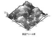
高温アニールの効果を確認するため、高温アニール前後の結晶性珪素膜の表面をSEMで観察した、図10に高温アニール前の観察写真を、図11に高温アニール後の観察写真を示す。図10、図11からも明らかなように、表面形状が高温アニール前後で明らかに異なっている。
【0029】
更に珪素膜の表面形状をAFM(原子間力顕微鏡)でも観察した。図11に高温アニール前の結晶性珪素膜のAFMによる観察像を示し、図12に高温アニール後の結晶性珪素膜のAFMによる観察像を示す。なお、観察範囲は図11、図12とも1.5μm×1.5μmの矩形の領域である。
【0030】
図11、図12から明らかなように、高温アニールの前後で結晶性珪素膜の表面形状は明らかに異なっている。高温アニール前・後とも結晶性珪素膜表面に凹凸があるが、高温アニール前では凸部が急峻でその頂部は尖っており、全体的に鋸歯状を呈している。このような凸部を有する表面がゲート絶縁膜とチャネル形成領域の界面となると、素子の特性に非常に悪影響を及ぼすと考えられる。対照的に、高温アニール後の凸部はなめらかであり、頂部は丸みを帯びているため、ゲート絶縁膜/チャネル形成領域界面特性は高温アニール前よりも改善される。
【0031】
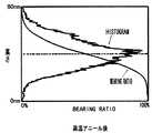
図9〜図13に示す観察像からでも、高温アニールよって結晶化珪素膜の表面が平坦化、平滑化されることが理解できるが、更に、高温アニール前後の表面形状の差異を定量化するため、AFM像の高さのHistogram(ヒストグラム)分布を算出した。更にこのHistogram分布のBearing Ratio曲線を算出した。Bearing Ratio曲線とはHistogram分布の累積度数を示すカーブである。
【0032】
図14、図15にAFM像の高さのヒストグラムとBearing Ratio曲線を示す。図14は高温アニール前のデータであり、ヒストグラムのピッチはおよそ0.16nmである。図15は高温アニール後のデータであり、ヒストグラムのピッチはおよそ0.20nmである。
【0033】
AFMによる測定領域は1.5μm×1.5μmである。Bearing Ratio曲線とはヒストグラムのデータの累積度数を表した曲線である。図14、図15の曲線は高さの最大値から累積したものであり、最大値から任意の高さの面積が全面積に占める割合(%)を示している。また、図14、図15において、グラフ中の点線で示す水平線はP−V値(Peak to Valley、高さの最大値と最小値の差分)の1/2の値を示す。
【0034】
更に、高温アニール前後の珪素膜において、それぞれ10の領域(1.5μm×1.5μmの矩形の領域)でAFM像を観察し、各観察領域での2-1(P−V値)におけるBearing Ratioを算出した。各観察領域におけるBearing Ratioとその統計データを図16に示す。
【0035】
図14、図15の曲線を比較すると、高温アニール前の高さ分布は低部側に偏っているが、高温アニール後ではその偏りが高いほうへシフトして、ヒストグラムはP−Vの1/2の位置に対して対称的になっている。このことはBearing Ratio曲線から容易に理解できる。
【0036】
高さが2-1(P−V)におけるBearing Ratioは図14では約20%であり、図15では約51%である。即ち、高さが最高値から2-1(P−V値)の範囲にある領域の面積が全面積に占める割合は、高温アニール前は約20%であるのに対して、高温アニール後は約51%である。この割合の違いからも、高温アニールによって、尖っていた頂部が丸みを帯びて、珪素膜の表面が平滑にされたことが理解できる。
【0037】
そこで本発明では、結晶性珪素膜の表面形状を2-1(P−V値)におけるBearing Ratioで定量化し、実験結果から2-1(P−V値)におけるBearing Ratio、即ち所定の観察領域において、高さが最大値から2-1(P−V値)の範囲にある領域が占める割合は、高温アニール前の膜では6〜28%の範囲にあり、高温アニール後の膜は29〜72%と推定される。
【0038】
なお、このBearing Ratioの範囲は図16の統計データから設定したものであり、2-1(P−V値)におけるBearing Ratioの平均値±3σから算出した値である。また、Bearing Ratioは高さの最大値から累積した値である。
【0039】
以上述べたように、本発明では、エキシマレーザーなど紫外光によって結晶化された結晶性半導体膜は表面が溶融されて結晶化されるため、所定の領域に対して高さが最大値から最大値と最小値の差分の1/2の範囲にある領域が占める割合は6〜28%となるが、この結晶性半導体膜を高温アニールよって処理することにより、この領域の占める割合が29〜72%へと変化し、膜表面の凸部の頂部を緩やかにすることができる。
【0040】
以上述べた実験は非晶質珪素膜にエキシマレーザーを照射した例であるが、本発明の結晶性珪素膜に照射した場合もほぼ同様な表面形状になると考えられる。本発明では高温アニール前のBearing Ratioは実験結果よりも大きくなると考えられ、高温アニール後のBearing Ratioは29〜72%、代表的には35〜60%の範囲にあると予測される。
【0041】
また、他の発明の構成は、 非晶質半導体薄膜上の一部又は全部の領域に対して当該非晶質半導体薄膜の結晶化を助長する触媒元素を添加する工程と、
第1熱処理を行い、前記非晶質半導体薄膜の一部又は全部の領域を結晶性半導体薄膜に変化させる工程と、
前記結晶性半導体薄膜に対してハロゲン元素を含む還元雰囲気中で第2熱処理を行う工程と、
を有することを特徴とするものである。
【0042】
この構成において第2熱処理は900〜1200℃の温度で行われる。この工程はハロゲン元素による金属元素のゲッタリング作用を狙ったものであり、非晶質半導体薄膜の結晶化に利用した触媒元素をハロゲン化して除去することを目的としている。
【0043】
【発明の実施の形態】
以上の構成からなる本願発明の実施形態について、以下に記載する実施例でもって詳細な説明を行うこととする。
【0044】
【実施例】
〔実施例1〕 本実施例では、本願発明を実施して基板上にTFTを作製する工程について説明する。説明には図1を用いる。
【0045】
まず、基板101として石英基板を用意した。基板101としては耐熱性の高い材料を選択しなければならない。石英基板の代わりにシリコン基板、セラミックス基板、結晶化ガラス基板等の耐熱性の高い材料を用いることもできる。
【0046】
ただし、石英基板を用いる場合は下地膜を設けても設けなくても良いが、他の材料を用いる時は下地膜として絶縁膜を設けることが好ましい。絶縁膜としては、酸化珪素膜(SiOx )、窒化珪素膜(Six Ny )、酸化窒化珪素膜(SiOx Ny )、窒化アルミニウム膜(AlxNy)のいずれか若しくはそれらの積層膜を用いると良い。
【0047】
また、耐熱性金属層と酸化珪素膜とを積層した下地膜を用いると放熱効果が大幅に高まるので有効である。放熱効果は上述の窒化アルミニウム膜と酸化珪素膜との積層構造でも十分な効果を示す。
【0048】
こうして絶縁表面を有する基板101が準備できたら、特開平7−130652号公報に記載された技術を利用して30nm厚の結晶性珪素膜102を形成した。詳細な手段については同公報に記載してあるので概略のみを説明する。
【0049】
まず本実施例では成膜ガスとしてジシラン(Si2H6)を用いた。減圧熱CVD法により20〜60nm厚の非晶質珪素膜を形成した。この時、膜中に混入するC(炭素)、N(窒素)及びO(酸素)といった不純物の濃度を徹底的に管理することが重要である。これらの不純物が多く存在すると結晶化の進行が妨げられるからである。
【0050】
本出願人は炭素濃度および窒素の濃度が5×10¹⁸atoms/cm3以下(好ましくは1×1018atoms/cm3以下、さらに好ましくは5×1017atoms/cm3以下、さらに好ましくは2×1017atoms/cm3以下)、酸素の濃度が1.5×1019atoms/cm3以下(好ましくは5×1018atoms/cm3以下、さらに好ましくは1×1018atoms/cm3以下)となる様に不純物濃度を管理した。また、金属元素は1×1017atoms/cm3となる様に管理した。成膜段階でこの様な濃度管理をしておけば、外部汚染さえ防げば、TFT作製工程中に不純物濃度が増加する様なことはない。なお、上記濃度はSIMS(質量二次イオン分析)の最低濃度領域における値である。
【0051】
非晶質珪素膜を成膜したら、非晶質珪素膜の全面(全部の領域)に対して非晶質珪素膜の結晶化を助長する触媒元素を添加した。具体的には、10ppmの酢酸ニッケル塩溶液をスピンコート法により塗布し、450℃1時間程度の水素出しを行った。
【0052】
そしてその後、不活性雰囲気、水素雰囲気または酸素雰囲気において500〜700℃(代表的には550〜650℃)の温度で4〜24時間の加熱処理を加えて結晶性珪素膜102を得た。この結晶性珪素膜102にはニッケルが1×10¹⁸〜1×10¹⁹atoms/cm3の濃度で残存する。(図1(A))
【0053】
なお、厳密に言うとスピンコートした時点では非晶質珪素膜中にニッケルは添加されていない。しかし、その後の水素だし工程でニッケルが非晶質珪素膜中へと容易に拡散するので実質的には添加工程と考えて良い。
【0054】
なお、減圧熱CVD法で形成した非晶質珪素膜と同等の膜質が得られるのであればプラズマCVD法を用いても良い。また、非晶質珪素膜の代わりに非晶質珪素膜中にゲルマニウムを含有させたシリコンゲルマニウム(SixxGe1-x(0<X<1)で表される)等の非晶質半導体薄膜を用いても良い。その場合、シリコンゲルマニウム中に含まれるゲルマニウムは5atomic%以下となる様にしておくことが望ましい。
【0055】
また、ニッケル以外にもコバルト(Co)、鉄(Fe)、パラジウム(Pd)、白金(Pt)、銅(Cu)、金(Au)といった格子侵入型の触媒元素またはゲルマニウム(Ge)、鉛(Pb)、錫(Sn)といった格子置換型(または溶融型)の触媒元素から選ばれた一種または複数種を用いることもできる。
【0056】
こうして図1(A)の状態が得られたら、次に紫外光又は赤外光を結晶性珪素膜102に対して照射した。本実施例ではXeClを励起ガスとしたエキシマレーザー照射によって熱処理を行った。エキシマレーザーのビーム形状は線状ビームであっても良いが、処理の均一性を高めるには面状ビームであることが望ましい。(図1(B))
【0057】
この時のレーザーエネルギーは100〜250mJ/cm2の条件で行うことが望ましい。エネルギーが強すぎると結晶粒界における結晶格子の連続性が損なわれてしまう可能性がある。なお、この紫外光又は赤外光を照射する工程は省略しても構わない。
【0058】
こうして結晶性が改善された結晶性珪素膜103を得た。次に、還元雰囲気中で900〜1200℃(好ましくは1000〜1150℃)の温度範囲の熱処理工程を行った。本実施例では水素雰囲気中で1050℃、20分の加熱処理を行った。(図1(C))
【0059】
還元雰囲気としては水素雰囲気、アンモニア雰囲気、水素又はアンモニアを含む不活性雰囲気(水素と窒素又は水素とアルゴンの混合雰囲気など)が望ましいが、不活性雰囲気でも結晶性珪素膜の表面の平坦化は可能である。しかし、還元作用を利用して自然酸化膜の還元を行うとエネルギーの高いシリコン原子が多く発生し、結果的に平坦化効果が高まるので好ましい。
【0060】
ただし、特に注意が必要なのは雰囲気中に含まれる酸素又は酸素化合物(例えばOH基)の濃度を10ppm以下(好ましくは1ppm以下)にしておくことである。さもないと水素による還元反応が起こらなくなってしまう。
【0061】
こうして結晶性珪素膜104を得た。結晶性珪素膜104は900〜1200℃という高い温度における水素熱処理によって非常に表面が平坦化された。また、高い温度で熱処理されるので、結晶粒内には殆ど積層欠陥等が存在しなかった。この点については後述する。
【0062】
こうして実質的に単結晶と見なせる結晶性珪素膜104が得られたら、次に結晶性珪素膜104をパターニングして活性層105を形成した。なお、本実施例では活性層を形成する前に水素雰囲気中での熱処理を行っているが、活性層を形成した後に行うこともできる。その場合、パターン化されていることによって結晶性珪素膜に発生する応力が緩和されるため好ましい。
【0063】
そして熱酸化工程を行って活性層105の表面に10nm厚の酸化珪素膜106を形成した。この酸化珪素膜106はゲート絶縁膜として機能する。また、活性層は5nmの厚さだけ膜減りするため膜厚は30nmとなった。最終的に5〜40nm厚の活性層(特にチャネル形成領域)が残る様に、熱酸化による膜減りを考慮して非晶質珪素膜(出発膜)の膜厚を決定しておくことが必要である。
【0064】
ゲート絶縁膜106を形成したら、その上に導電性を有する多結晶珪素膜を形成し、パターニングによりゲート配線107を形成した。(図1(D))
【0065】
なお、本実施例ではゲート配線としてN型導電性を持たせた多結晶珪素膜を利用するが、材料はこれに限定されるものではない。特に、ゲート配線の抵抗を下げるにはタンタル、タンタル合金又はタンタルと窒化タンタルとの積層膜を用いることも有効である。さらに低抵抗なゲート配線を狙うならば銅や銅合金を用いても有効である。
【0066】
図1(D)の状態が得られたら、N型導電性又はP型導電性を付与する不純物を添加して不純物領域108を形成した。この時の不純物濃度は後のLDD領域の不純物濃度を鑑みて決定した。本実施例では1×10¹⁸atoms/cm3の濃度で砒素を添加したが、不純物も濃度も本実施例に限定される必要はない。
【0067】
次に、ゲート配線107の表面に5〜10nm程度の薄い酸化珪素膜109を形成した。これは熱酸化法やプラズマ酸化法を用いて形成すれば良い。この酸化珪素膜109の形成には、次のサイドウォール形成工程でエッチングストッパーとして機能させる目的がある。
【0068】
エッチングストッパーとなる酸化珪素膜109を形成したら、窒化珪素膜を形成してエッチバックを行い、サイドウォール110を形成した。こうして図1(E)の状態を得た。
【0069】
なお、本実施例ではサイドウォールとして窒化珪素膜を用いたが、多結晶珪素膜や非晶質珪素膜を用いることもできる。勿論、ゲート配線の材料が変われば、それに応じてサイドウォールとして用いることのできる材料も変わることは言うまでもない。
【0070】
次に、再び先程と同一導電型の不純物を添加した。この時に添加する不純物濃度は先程の工程よりも高い濃度とした。本実施例では不純物として砒素を用い、濃度は1×10²¹atoms/cm3とするがこれに限定する必要はない。この不純物の添加工程によりソース領域111、ドレイン領域112、LDD領域113及びチャネル形成領域114が画定した。(図1(F))
【0071】
こうして各不純物領域が形成されたらファーネスアニール、レーザーアニール又はランプアニール等の熱処理により不純物の活性化を行った。
【0072】
次に、ゲート配線107、ソース領域111及びドレイン領域112の表面に形成された酸化珪素膜を除去し、それらの表面を露呈させた。そして、5nm程度のコバルト膜(図示せず)を形成して熱処理工程を行った。この熱処理によりコバルトとシリコンとの反応が起こり、シリサイド層(コバルトシリサイド層)115が形成された。(図1(G))
【0073】
この技術は公知のサリサイド技術である。従って、コバルトの代わりにチタンやタングステンを用いても構わないし、熱処理条件等は公知技術を参考にすれば良い。本実施例では赤外光を照射して熱処理工程を行った。
【0074】
こうしてシリサイド層115を形成したら、コバルト膜を除去した。その後、1μm厚の層間絶縁膜116を形成した。層間絶縁膜116としては、酸化珪素膜、窒化珪素膜、酸化窒化珪素膜又は樹脂膜(ポリイミド、アクリル、ポリアミド、ポリイミドアミド、ベンゾシクロブテン(BCB)等)を用いれば良い。また、これらの絶縁膜を自由な組み合わせで積層しても良い。
【0075】
次に、層間絶縁膜116にコンタクトホールを形成してアルミニウムを主成分とする材料でなるソース配線117及びドレイン配線118を形成した。最後に素子全体に対して水素雰囲気中で300℃2時間のファーネスアニールを行い、水素化を完了した。
【0076】
こうして、図1(G)に示す様なTFTが得られた。なお、本実施例で説明した構造は一例であって本願発明を適用しうるTFT構造はこれに限定されない。従って、公知のあらゆる構造のTFTに対して適用可能である。また、結晶性珪素膜104を形成した以降の工程における数値条件も本実施例に限定される必要はない。さらには、公知のチャネルドープ工程(しきい値電圧を制御するための不純物添加工程)を本実施例のどこかに導入してもなんら問題はない。
【0077】
また、本実施例では出発膜である非晶質珪素膜を成膜する段階で徹底的にC、N、Oといった不純物の濃度を管理しているため、完成したTFTの活性層中に含まれる各不純物濃度は、炭素及び窒素の濃度が5×10¹⁸atoms/cm3以下(好ましくは1×1018atoms/cm3以下、さらに好ましくは5×1017atoms/cm3以下、さらに好ましくは2×1017atoms/cm3以下)、酸素の濃度が1.5×1019atoms/cm3以下(好ましくは5×1018atoms/cm3以下、さらに好ましくは1×1018atoms/cm3以下)のままであった。また、金属元素は1×1017atoms/cm3以下であった。
【0078】
また、本願発明はトップゲート構造に限らず、逆スタガ型TFTに代表されるボトムゲート構造に対しても容易に適用することが可能であることは言うまでもない。
【0079】
また、本実施例ではNチャネル型TFTを例にとって説明したが、公知技術と組み合わせればPチャネル型TFTを作製することも容易である。さらに公知技術を組み合わせれば同一基板上にNチャネル型TFTとPチャネル型TFTとを形成して相補的に組み合わせ、CMOS回路を形成することも可能である。
【0080】
さらに、図1(G)の構造においてドレイン配線118と電気的に接続する画素電極(図示せず)を公知の手段で形成すればアクティブマトリクス型表示装置の画素スイッチング素子を形成することも容易である。
【0081】
即ち、本願発明は液晶表示装置やEL(エレクトロルミネッセンス)表示装置などのアクティブマトリクス型の電気光学装置を作製する際にも実施することが可能である。
【0082】
〔活性層の結晶構造に関する知見〕 上記作製工程に従って形成した活性層は、微視的に見れば複数の針状又は棒状の結晶(以下、棒状結晶と略記する)が集まって並んだ結晶構造を有していると考えられる。このことはTEM(透過型電子顕微鏡法)による観察で容易に確認することができる。更に、結晶粒界における結晶格子の連続性が非常に高い結晶構造を有していることも予測される。
【0083】
この結晶粒界の連続性は電子線回折、X線回折を利用して確認することができる。結晶格子の連続性が高い結晶性珪素でなる活性層の表面(チャネルを形成する部分)が結晶軸に多少のずれが含まれているものの主たる配向面が{110}面でり、{110}面に対応する回折斑点がきれいに現れているが、各斑点は同心円上に分布を持つことになる。
【0084】
その様子を模式的に図8に示す。図8(A)は電子線回折パターンの一部を模式的に示した図である。図8(A)において、1201で示される複数の輝点は〈110〉入射に対応する回折スポットである。複数の回折スポット1201は電子線照射エリアの中心点1202を中心にして同心円上に分布している。
【0085】
ここで、点線で囲まれた領域1203を拡大したものを図8(B)に示す。図8(B)に示す様に、照射エリアの中心点1202に対して回折スポット1201が分布(ゆらぎ)を持っていることが判る。
【0086】
電子線照射エリアの中心点1202から回折スポット1201に対して引いた接線1204と、電子線照射エリアの中心点1202と回折スポットの中心点1205とを結ぶ線分とがなす角は2°以下になる。この時、接線は2本引けるので、回折スポット1201の広がりは結局±2°以内の範囲に収まることになる。
【0087】
この傾向は実際の電子線回折パターンの全域で見受けられ、全体としては±2°以内(典型的には±1.5°以内、好ましくは±0.5°以内)に収まっている。回折スポットが分布を持つとはこの様なことを指している。
【0088】
また、この様な回折スポットの分布は、同一の結晶軸を有する個々の結晶粒が互いに結晶軸周りに回転した配置で集合している際に現れることが知られている。即ち、ある結晶面内に含まれる特定の軸(軸Aと呼ぶ)と、隣接する他の結晶面内に含まれる軸Aと等価な軸(軸Bと呼ぶ)とがなす角を回転角と呼ぶと、その回転角に相当する分だけ回折スポットの現れる位置がずれるのである。
【0089】
従って、複数の結晶粒が互いにある回転角を持った位置関係で集合している場合、個々の結晶粒が示す回折スポットの集合体として一つの電子線回折パターンを観察することができる。
【0090】
±2°以内(典型的には±1.5°以内、好ましくは±0.5°以内)の範囲で回折スポットが広がりを持つ場合、隣接する結晶粒の間では等価な軸がなす回転角の絶対値が4°以内(典型的には3°以内、好ましくは1°以内)であることを意味している。
【0091】
なお、結晶軸が〈110〉軸の場合、結晶面内に含まれる等価な軸としては〈111〉軸が挙げられるが、本願発明の結晶性半導体薄膜では〈111〉軸同士が70.5(又は70.4という説もある)の回転角をもって接した結晶粒界が多く見られる。この場合も等価な軸が70.5°±2°の回転角をもっていると考えられる。
【0092】
即ち、このような場合には、結晶粒の間では、等価な軸又は等価な軸に対して70.5°の回転関係にある軸がなす回転角の絶対値が4°以内(典型的には3°以内、好ましくは1°以内)であるとも言える。
【0093】
また、結晶粒界をHR−TEM(高分解能透過型電子顕微鏡法)により観察して、結晶粒界において結晶格子に連続性があることを確認することもできる。HR−TEMでは、観察される格子縞が結晶粒界において連続的に繋がっているか、否かが容易に確認できる。
【0094】
なお、結晶粒界における結晶格子の連続性は、その結晶粒界が「平面状粒界」と呼ばれる粒界であることに起因する。本明細書における平面状粒界の定義は、「Characterization of High-Efficiency Cast-Si Solar Cell Wafersby MBIC Measurement;Ryuichi Shimokawa and Yutaka Hayashi,Japanese Journal of Applied Physics vol.27,No.5,pp.751-758,1988」に記載された「Planar boundary 」である。
【0095】
上記論文によれば、平面状粒界には双晶粒界、特殊な積層欠陥、特殊なtwist 粒界などが含まれる。この平面状粒界は電気的に不活性であるという特徴を持つ。即ち、結晶粒界でありながらキャリアの移動を阻害するトラップとして機能しないため、実質的に存在しないと見なすことができる。
【0096】
特に結晶軸(結晶面に垂直な軸)が〈110〉軸である場合、{211}双晶粒界はΣ3の対応粒界とも呼ばれる。Σ値は対応粒界の整合性の程度を示す指針となるパラメータであり、Σ値が小さいほど整合性の良い粒界であることが知られている。
【0097】
本出願人が本願発明の方法を実施して得た結晶性珪素膜は、結晶粒界の殆ど(90%以上、典型的には95%以上)がΣ3の対応粒界、即ち{211}双晶粒界にすることができる。
【0098】
二つの結晶粒の間に形成された結晶粒界において、両方の結晶の面方位が{110}である場合、{111}面に対応する格子縞がなす角をθとすると、θ=70.5°の時にΣ3の対応粒界となることが知られている。
【0099】
本願発明の結晶性珪素膜は、結晶粒界において隣接する結晶粒の各格子縞が約70.5°の角度をもって連続した、即ち結晶粒界が{211}双晶粒界である結晶性珪素膜とであるという結論に辿り着いた。
【0100】
なお、θ= 38.9 °の時にはΣ9の対応粒界となるが、この様な他の結晶粒界も存在した。
【0101】
この様な対応粒界は、同一面方位の結晶粒間にしか形成されない。即ち、結晶性珪素膜は面方位が概略{110}で揃っている場合に初めて、広範囲に渡ってこの様な対応粒界が形成される。
【0102】
この様な結晶構造(正確には結晶粒界の構造)は、結晶粒界において異なる二つの結晶粒が極めて整合性よく接合していることを示している。即ち、結晶粒界において結晶格子が連続的に連なり、結晶欠陥等に起因するトラップ準位を非常に作りにくい構成となっている。従って、この様な結晶構造を有する結晶性半導体薄膜は実質的に結晶粒界が存在しないと見なすことができる。
【0103】
またさらに、図1(C)に示す還元雰囲気における熱処理工程によって結晶粒内に存在する欠陥が殆ど消滅させることができる。これはこの熱処理工程の前後で欠陥数が大幅に低減されていることから確認できる。
【0104】
この欠陥数の差は電子スピン共鳴分析(Electron Spin Resonance :ESR)によってスピン密度の差として測定される。実施例1の作製工程によって、結晶性珪素膜のスピン密度は少なくとも 5×10¹⁷spins/cm3以下(好ましくは 3×10¹⁷spins/cm3 以下)とすることができる。ただし、この測定値は現存する測定装置の検出限界に近いので、実際のスピン密度はさらに低いと予想される。
【0105】
また、この熱処理工程は還元雰囲気、特に水素雰囲気で行われるので僅かに残った欠陥も水素終端されて不活性化している。従って、結晶粒内の欠陥は実質的に存在しないと見なしてよいと考える。
【0106】
以上の事から、本願発明を実施することで得られた結晶性半導体薄膜は結晶粒内及び結晶粒界が実質的に存在しないため、単結晶半導体薄膜又は実質的な単結晶半導体薄膜と考えて良い。
【0107】
〔TFTの電気特性に関する知見〕 上述した粒界の連続性の高い結晶性珪素膜で作製されたTFTは純粋な単結晶珪素を用いたMOSFETに匹敵する電気特性を示す。
【0108】
(1)スイッチング性能(オン/オフ動作切り換えの俊敏性)の指標となるサブスレッショルド係数が、Nチャネル型TFTおよびPチャネル型TFTともに60〜100mV/decade(代表的には60〜85mV/decade )と小さい。(2)TFTの動作速度の指標となる電界効果移動度(μFE)が、Nチャネル型TFTで 200〜650cm2/Vs (代表的には300〜500cm2/Vs )、Pチャネル型TFTで100〜300cm2/Vs (代表的には 150〜200cm2/Vs )と大きくすることが可能である。(3)TFTの駆動電圧の指標となるしきい値電圧(Vth)が、Nチャネル型TFTで-0.5〜1.5 V、Pチャネル型TFTで-1.5〜0.5 Vと小さくすることができる。
【0109】
以上の様に、極めて優れたスイッチング特性および高速動作特性が実現可能であることが確認されている。
【0110】
〔回路特性に関する知見〕 例えば、リングオシレータによる周波数特性が上げられる。。リングオシレータとはCMOS構造でなるインバータ回路を奇数段リング状に接続した回路であり、インバータ回路1段あたりの遅延時間を求めるのに利用される。リングオシレータの構成は次の様になっている。 段数:9段 TFTのゲイト絶縁膜の膜厚:30nm及び50nm TFTのゲイト長: 0.6μm
この様なリングオシレータによって発振周波数は最大値で1.04GHzとすることができる。
【0111】
またLSI回路のTEGの一つであるシフトレジスタを作製して動作周波数は、ゲイト絶縁膜の膜厚30nm、ゲイト長 0.6μm、電源電圧5V、段数50段のシフトレジスタ回路の場合では、100 MHzの出力パルスを発生させることが可能である。
【0112】
以上の様なリングオシレータおよびシフトレジスタの驚異的なデータは、上述した連続性のある結晶粒界をもつ結晶性珪素を用いたTFTが単結晶シリコンを利用したIGFETに匹敵する、若しくは凌駕する性能を有していることを示している。
【0113】
(実施例2) 実施例1では非晶質珪素膜の全面(全部の領域)に対して結晶化を助長する触媒元素を添加しているが、一部の領域に対して選択的に添加する方法をとっても良い。その場合には、特開平7−130652号公報の実施例2に記載の手段を用いた。
【0114】
概略的には、非晶質珪素膜を成膜したら選択的に絶縁膜を設け、その絶縁膜をマスクとして結晶化を助長する触媒元素を添加した。具体的には酸化珪素膜でなるマスクを設けた後、酢酸ニッケル塩溶液をスピンコート法により塗布して水素だし工程(条件は実施例1と同様)を行った。
【0115】
この状態で結晶化のための熱処理工程を行うと、ニッケルと直接接触する部分から結晶化が開始され、マスクの下に潜り込む様な形で結晶化が進行した。これにより基板とほぼ平行な方向に結晶成長した結晶領域を得ることができた。本出願人はこの様な特徴を有する結晶領域を横成長領域と呼んでいる。この横成長領域はニッケルが直接添加されないので、結晶化後に含まれるニッケル濃度が1×10¹⁸〜5×10¹⁸atoms/cm3程度と、直接触れて結晶化した場合に較べて1桁程度低い。
【0116】
従って、パターニングによって横成長領域のみを島状に残し、それをTFTの活性層とすることでニッケルの如き触媒元素の含有量の少ない活性層を得ることができた。
【0117】
本実施例の場合、まず結晶化工程までは上述の手段で行い、形成された結晶性珪素膜(実際にはニッケルが添加された部分と横成長領域のみが結晶化し、その他の部分は非晶質のままである)を得た。この結晶構造は、微視的には実施例1と同様であるが、個々の棒状結晶が巨視的には特定の方向性もって並んでいる点が実施例1と異なる。
【0118】
そして、実施例1で説明した図1(B)〜図1(G)までの工程を経てTFTを形成した。こうして形成されたTFT及びその様なTFTで組まれた回路は実施例1と同様の優れた電気特性を示すものであった。
【0119】
(実施例3) 本実施例では、実施例1又は実施例2において900〜1200℃の水素アニール工程を行う前に結晶性珪素膜中から珪素の結晶化を助長する触媒元素(ニッケルを例にとる)を除去する工程を行う場合の例について説明する。
【0120】
本実施例の場合、膜中のニッケルを除去するためにハロゲン元素のゲッタリング作用を利用した。これはハロゲン元素とニッケルとが化合することで揮発性のハロゲン化ニッケルになることを利用した技術である。この技術は結晶性珪素膜をハロゲン元素を含む雰囲気中に置き、700〜1150℃(代表的には950〜1100℃)の熱処理工程を0.5〜8時間程度行うという構成から成り立つ。
【0121】
本実施例では酸素と塩化水素とを混合したガス中に処理基板を置き、950℃1時間の熱処理工程を行った。この工程により結晶性珪素膜中に残存するニッケル濃度を1×10¹⁷atoms/cm3以下にまで低減することができた。なお、1×1017atoms/cm3付近はSIMS(質量二次イオン分析)の測定下限であるため、実際には1×1014atoms/cm3〜1×1016atoms/cm3くらいの濃度で存在すると予想される。
【0122】
また、このハロゲン元素によるゲッタリング工程は900〜1200℃の温度で行う水素アニール工程の前に行っても後に行っても良い。さらに、水素アニール工程とゲッタリング工程とを兼ねることも可能である。その場合、水素雰囲気中に0.1〜5wt%のハロゲン化水素(代表的には塩化水素)を混合した雰囲気中で900〜1200℃の熱処理工程を行えば良い。還元雰囲気中でハロゲン元素によるゲッタリングを行うと、結晶性珪素膜が酸化されないので酸化珪素膜の異常成長といった問題は全く起こらない。
【0123】
本実施例を採用することで、結晶性珪素膜中から触媒元素を除去又は低減することができる。触媒元素の濃度は1×10¹⁷atoms/cm3以下にまで低減されるので、触媒元素の存在によってTFT特性(特にオフ電流値)がばらつく様なことを防ぐことができる。
【0124】
(実施例4) 本実施例では、実施例1又は実施例2において900〜1200℃の水素アニール工程を行う前に結晶性珪素膜中から珪素の結晶化を助長する触媒元素(ニッケルを例にとる)を除去するに際して実施例3とは異なる手段を用いる場合について説明する。
【0125】
説明には図2を用いる。まず、実施例2に示された工程を経て非晶質珪素膜の結晶化を行った。具体的には石英基板201上に非晶質珪素膜(図示せず)を形成し、その上に酸化珪素膜でなるマスク202を形成した。そして、その状態でニッケル塩をスピンコートして結晶化のための熱処理工程を行った。本実施例では熱処理条件を570℃14時間とした。この熱処理工程(結晶化工程)によって横成長領域203を得た。(図2(A))
【0126】
次に、マスク202をそのままマスクとして活用して15族から選ばれた元素(本実施例ではリン)を添加した。添加方法はイオン注入法、プラズマドーピング法、気相拡散法など公知のどの様な手段を用いても構わない。(図2(B))
【0127】
こうしてマスク202の開孔部によって露呈した結晶性珪素膜中にリンが添加された領域204が形成された。本実施例ではこの領域を便宜上ゲッタリング領域と呼ぶことにする。ゲッタリング領域204に含まれるリン濃度は1×10¹⁹〜1×10²¹atoms/cm3となる様に添加量を調節した。
【0128】
ゲッタリング領域204を形成した後、550〜750℃(好ましくは600〜650℃)の温度範囲で2〜24時間(好ましくは8〜12時間)の熱処理を行うことでゲッタリング工程がなされる。本実施例では600℃12時間の熱処理工程を行った。(図2(C))
【0129】
その結果、横成長領域203に含まれていたニッケルはゲッタリング領域204で捉えられ(ゲッタリングされ)、ニッケル濃度の大幅に低減された横成長領域205が得られた。この横成長領域205中に含まれるニッケル濃度は、1×10¹⁷atoms/cm3以下であった。ただし、実施例3でも述べた様に1×1017atoms/cm3付近はSIMS(質量二次イオン分析)の測定下限であるため、実際には1×1016atoms/cm3以下くらいまでは低減されていると予想される。
【0130】
次に、パターニングを施して横成長領域205のみでなる活性層206、207を形成した。そして、水素雰囲気中において1050℃1時間の熱処理工程を行い、活性層表面の平坦化と結晶性の改善とを行った。勿論、熱処理条件は本実施例に限定されない。
【0131】
活性層を形成してから水素アニールを行ったのは、ゲッタリング領域が残ったまま800℃を超える熱処理を行うと、リンが横成長領域の方へと逆拡散してしまうからである。本実施例の様にゲッタリング領域を完全に除去してから水素アニールを行った方が、チャネル形成領域にリンが混入しないので望ましい。
【0132】
こうして図2(D)の状態を得たら、後は実施例1に示した作製工程に従ってTFTを作製すれば良い。勿論、公知の他の手段によりTFTを作製しても本願発明の効果を損ねるものではない。
【0133】
また、図2(D)の工程(水素アニール工程)を行う前に結晶性珪素膜(またはパターニング後の活性層)に対して紫外光又は赤外光を照射する工程を行っても構わない。その場合には実施例1に示した様に、結晶粒界における結晶格子の連続性を壊さない様に注意する必要がある。
【0134】
また、ゲッタリング工程(図2(B)及び図2(C))を行う前に図2(D)の熱処理工程を行っても構わない。その場合には一旦マスク202を除去してから水素アニールを行い、その後でマスクを形成し直してゲッタリング工程を行う必要がある。
【0135】
(実施例5) 本実施例ではリンを用いて触媒元素(本実施例ではニッケル)をゲッタリングする上で、ソース領域及びドレイン領域を利用する場合の例について説明する。説明には図3を用いる。
【0136】
まず実施例1の作製工程に従ってNチャネル型TFT301及びPチャネル型TFT302を形成した。Pチャネル型TFTの作製工程例については実施例1で説明していないが、構造はNチャネル型TFTと同一であるので、活性層に添加する不純物の導電型を13族から選ばれた元素(代表的にはボロン)に変えれば良い。
【0137】
こうして図3(A)の状態を得た。Nチャネル型TFT301のソース領域303及びドレイン領域304は5×10²⁰atoms/cm3の濃度でリンが添加されて形成されている。また、Pチャネル型TFT302のソース領域305及びドレイン領域306は5×1020atoms/cm3の濃度のリンと1.5×1021atoms/cm3の濃度のボロンとが添加されている。
【0138】
次に図3(A)の状態で500〜650℃、1〜12時間(本実施例では500℃1時間)の熱処理工程(ゲッタリング工程)を行った。この時、ソース領域303、305及びドレイン領域304、306が各々ゲッタリング領域として機能した。Pチャネル型TFT305側では、リンよりもボロンの濃度の方が高いにも関わらず良好にニッケルをゲッタリングすることが可能であった。
【0139】
このゲッタリング工程では、ゲート配線直下のチャネル形成領域から隣接するソース領域及びドレイン領域に向かって、ニッケルが移動してゲッタリングされる。そのため、チャネル形成領域中のニッケル濃度は1×10¹⁷atoms/cm3以下(おそらくは1×1016atoms/cm3以下)にまで低減された。
【0140】
なお、本実施例に示したゲッタリング工程は実施例1〜実施例4のどの実施例とも組み合わせることが可能である。
【0141】
(実施例6) 本実施例では、本願発明によって作製された反射型液晶表示装置の例を図4に示す。画素TFT(画素スイッチング素子)の作製方法やセル組工程は公知の手段を用いれば良いので詳細な説明は省略する。
【0142】
図4(A)において11は絶縁表面を有する基板(酸化珪素膜を設けたセラミックス基板)、12は画素マトリクス回路、13はソースドライバー回路、14はゲイトドライバー回路、15は対向基板、16はFPC(フレキシブルプリントサーキット)、17は信号処理回路である。信号処理回路17としては、D/Aコンバータ、γ補正回路、信号分割回路などの従来ICで代用していた様な処理を行う回路を形成することができる。勿論、ガラス基板上にICチップを設けて、ICチップ上で信号処理を行うことも可能である。
【0143】
さらに、本実施例では液晶表示装置を例に挙げて説明しているが、アクティブマトリクス型の表示装置であればEL(エレクトロルミネッセンス)表示装置やEC(エレクトロクロミックス)表示装置に本願発明を適用することも可能であることは言うまでもない。
【0144】
ここで図4(A)のドライバー回路13、14を構成する回路の一例を図4(B)に示す。なお、TFT部分については既に実施例1で説明しているので、ここでは必要箇所のみの説明を行う。
【0145】
図4(B)において、401、402はNチャネル型TFT、403はPチャネル型TFTであり、401と403のTFTでCMOS回路を構成している。404は窒化珪素膜/酸化珪素膜/樹脂膜の積層膜でなる絶縁層、その上にはチタン配線405が設けられ、前述のCMOS回路とTFT402とが電気的に接続されている。チタン配線はさらに樹脂膜でなる絶縁層406で覆われている。二つの絶縁層404、406は平坦化膜としての機能も有している。
【0146】
また、図4(A)の画素マトリクス回路12を構成する回路の一部を図4(C)に示す。図4(C)において、407はダブルゲート構造のNチャネル型TFTでなる画素TFTであり、画素領域内に大きく広がる様にしてドレイン配線408が形成されている。なお、ダブルゲート構造以外にシングルゲート構造やトリプルゲート構造などを採用しても構わない。
【0147】
その上には絶縁層404が設けられ、その上にチタン配線405が設けられている。この時、絶縁層404の一部には凹部が落とし込み部が形成され、最下層の窒化シリコン及び酸化シリコンのみが残される。これによりドレイン配線408とチタン配線405との間で補助容量が形成される。
【0148】
また、画素マトリクス回路内に設けられたチタン配線405はソース・ドレイン配線と後の画素電極との間において電界遮蔽効果をもたらす。さらに、複数設けられた画素電極間の隙間ではブラックマスクとしても機能する。
【0149】
そして、チタン配線405を覆って絶縁層406が設けられ、その上に反射性導電膜でなる画素電極409が形成される。勿論、画素電極409の表面に反射率を上げるための工夫をなしても構わない。
【0150】
また、実際には画素電極409の上に配向膜や液晶層が設けられるが、ここでの説明は省略する。
【0151】
本願発明を用いて以上の様な構成でなる反射型液晶表示装置を作製することができる。勿論、公知の技術と組み合わせれば容易に透過型液晶表示装置を作製することもできる。さらに、公知の技術と組み合わせればアクティブマトリクス型のEL表示装置も容易に作製することができる。
【0152】
また、図面では区別していないが画素マトリクス回路を構成する画素TFTと、ドライバー回路や信号処理回路を構成するCMOS回路とでゲート絶縁膜の膜厚を異ならせることも可能である。
【0153】
画素マトリクス回路ではTFTに印加される駆動電圧が高いので50〜200nm程度の膜厚のゲート絶縁膜が必要である。一方、ドライバー回路や信号処理回路ではTFTに印加される駆動電圧は低く、逆に高速動作が求められるのでゲート絶縁膜の膜厚を3〜30nm程度と画素TFTよりも薄くすることが有効である。
【0154】
(実施例7) 上記実施例によって作製された液晶表示装置には、TN液晶以外にも様々な液晶を用いることが可能である。例えば、1998, SID, "Characteristics and Driving Scheme of Polymer-Stabilized Monostable FLCD Exhibiting Fast Response Time and High Contrast Ratio with Gray-Scale Capability" by H. Furue et al.や、1997, SID DIGEST, 841, "A Full-Color Thresholdless Antiferroelectric LCD Exhibiting Wide Viewing Angle with Fast Response Time" by T. Yoshida et al.や、1996, J. Mater. Chem. 6(4), 671-673, "Thresholdless antiferroelectricity in liquid crystals and its application to displays" by S. Inui et al.や、米国特許第5594569 号に開示された液晶を用いることが可能である。
【0155】
ある温度域において反強誘電相を示す液晶を反強誘電性液晶という。反強誘電性液晶を有する混合液晶には、電場に対して透過率が連続的に変化する電気光学応答特性を示す、無しきい値反強誘電性混合液晶と呼ばれるものがある。この無しきい値反強誘電性混合液晶は、V字型の電気光学応答特性を示すものがあり、その駆動電圧が約±2.5V程度(セル厚約1μm〜2μm)のものも見出されている。
【0156】
ここで、V字型の電気光学応答を示す無しきい値反強誘電性混合液晶の印加電圧に対する光透過率の特性を示す例を図9に示す。図9に示すグラフの縦軸は透過率(任意単位)、横軸は印加電圧である。なお、液晶表示装置の入射側の偏光板の透過軸は、液晶表示装置のラビング方向にほぼ一致する無しきい値反強誘電性混合液晶のスメクティック層の法線方向とほぼ平行に設定されている。また、出射側の偏光板の透過軸は、入射側の偏光板の透過軸に対してほぼ直角(クロスニコル)に設定されている。
【0157】
図9に示されるように、このような無しきい値反強誘電性混合液晶を用いると、低電圧駆動かつ階調表示が可能となることがわかる。
【0158】
このような低電圧駆動の無しきい値反強誘電性混合液晶をアナログドライバを有する液晶表示装置に用いた場合には、画像信号のサンプリング回路の電源電圧を、例えば、5V〜8V程度に抑えることが可能となる。よって、ドライバの動作電源電圧を下げることができ、液晶表示装置の低消費電力化および高信頼性が実現できる。
【0159】
また、このような低電圧駆動の無しきい値反強誘電性混合液晶をデジタルドライバを有する液晶表示装置に用いた場合にも、D/A変換回路の出力電圧を下げることができるので、D/A変換回路の動作電源電圧を下げることができ、ドライバの動作電源電圧を低くすることができる。よって、液晶表示装置の低消費電力化および高信頼性が実現できる。
【0160】
よって、このような低電圧駆動の無しきい値反強誘電性混合液晶を用いることは、比較的LDD領域(低濃度不純物領域)の幅が小さなTFT(例えば、0nm〜500nmまたは0nm〜200nm)を用いる場合においても有効である。
【0161】
また、一般に、無しきい値反強誘電性混合液晶は自発分極が大きく、液晶自体の誘電率が高い。このため、無しきい値反強誘電性混合液晶を液晶表示装置に用いる場合には、画素に比較的大きな保持容量が必要となってくる。よって、自発分極が小さな無しきい値反強誘電性混合液晶を用いるのが好ましい。また、液晶表示装置の駆動方法を線順次駆動とすることにより、画素への階調電圧の書き込み期間(ピクセルフィードピリオド)を長くし、保持容量が小くてもそれを補うようにしてもよい。
【0162】
なお、このような無しきい値反強誘電性混合液晶を用いることによって低電圧駆動が実現されるので、液晶表示装置の低消費電力が実現される。
【0163】
なお、図9に示すような電気光学特性を有する液晶であれば、いかなるものも本発明の液晶表示装置の表示媒体として用いることができる。
【0164】
(実施例8) 本願発明は従来のIC技術全般に適用することが可能である。即ち、現在市場に流通している全ての半導体回路に適用できる。例えば、ワンチップ上に集積化されたRISCプロセッサ、ASICプロセッサ等のマイクロプロセッサに適用しても良いし、D/Aコンバータ等の信号処理回路から携帯機器(携帯電話、PHS、モバイルコンピュータ)用の高周波回路に適用しても良い。
【0165】
図5に示すのは、マイクロプロセッサの一例である。マイクロプロセッサは典型的にはCPUコア21、RAM22、クロックコントローラ23、キャッシュメモリ24、キャッシュコントローラ25、シリアルインターフェース26、I/Oポート27等から構成される。
【0166】
勿論、図5に示すマイクロプロセッサは簡略化した一例であり、実際のマイクロプロセッサはその用途によって多種多様な回路設計が行われる。
【0167】
しかし、どの様な機能を有するマイクロプロセッサであっても中枢として機能するのはIC(Integrated Circuit)28である。IC28は半導体チップ29上に形成された集積化回路をセラミック等で保護した機能回路である。
【0168】
そして、その半導体チップ29上に形成された集積化回路を構成するのが本願発明の構造を有するNチャネル型TFT30、Pチャネル型TFT31である。なお、基本的な回路はCMOS回路を最小単位として構成することで消費電力を抑えることができる。
【0169】
また、本実施例に示したマイクロプロセッサは様々な電子機器に搭載されて中枢回路として機能する。代表的な電子機器としてはパーソナルコンピュータ、携帯型情報端末機器、その他あらゆる家電製品が挙げられる。また、車両(自動車や電車等)の制御用コンピュータなども挙げられる。
【0170】
(実施例9)
本願発明を実施して形成されたCMOS回路や画素マトリクス回路は様々な電気光学装置(アクティブマトリクス型液晶ディスプレイ、アクティブマトリクス型ELディスプレイ、アクティブマトリクス型ECディスプレイ)に用いることができる。即ち、それら電気光学装置を表示媒体として組み込んだ電子機器全てに本願発明を実施できる。
【0171】
その様な電子機器としては、ビデオカメラ、デジタルカメラ、プロジェクター(リア型またはフロント型)、ヘッドマウントディスプレイ(ゴーグル型ディスプレイ)、カーナビゲーション、パーソナルコンピュータ、携帯情報端末(モバイルコンピュータ、携帯電話または電子書籍等)などが挙げられる。それらの一例を図6及び図7に示す。
【0172】
図6(A)はパーソナルコンピュータであり、本体2001、画像入力部2002、表示装置2003、キーボード2004で構成される。本願発明を画像入力部2002、表示装置2003やその他の信号制御回路に適用することができる。
【0173】
図6(B)はビデオカメラであり、本体2101、表示装置2102、音声入力部2103、操作スイッチ2104、バッテリー2105、受像部2106で構成される。本願発明を表示装置2102、音声入力部2103やその他の信号制御回路に適用することができる。
【0174】
図6(C)はモバイルコンピュータ(モービルコンピュータ)であり、本体2201、カメラ部2202、受像部2203、操作スイッチ2204、表示装置2205で構成される。本願発明は表示装置2205やその他の信号制御回路に適用できる。
【0175】
図6(D)はゴーグル型ディスプレイであり、本体2301、表示装置2302、アーム部2303で構成される。本発明は表示装置2302やその他の信号制御回路に適用することができる。
【0176】
図6(E)はプログラムを記録した記録媒体(以下、記録媒体と呼ぶ)を用いるプレーヤーであり、本体2401、表示装置2402、スピーカ部2403、記録媒体2404、操作スイッチ2405で構成される。なお、この装置は記録媒体としてDVD(Digital Versatile Disc)、CD等を用い、音楽鑑賞や映画鑑賞やゲームやインターネットを行うことができる。本発明は表示装置2402やその他の信号制御回路に適用することができる。
【0177】
図6(F)はデジタルカメラであり、本体2501、表示装置2502、接眼部2503、操作スイッチ2504、受像部(図示しない)で構成される。本願発明を表示装置2502やその他の信号制御回路に適用することができる。
【0178】
図7(A)はフロント型プロジェクターであり、表示装置2601、スクリーン2602で構成される。本発明は表示装置やその他の信号制御回路に適用することができる。
【0179】
図7(B)はリア型プロジェクターであり、本体2701、表示装置2702、ミラー2703、スクリーン2704で構成される。本発明は表示装置やその他の信号制御回路に適用することができる。
【0180】
なお、図7(C)は、図7(A)及び図7(B)中における表示装置2601、2702の構造の一例を示した図である。表示装置2601、2702は、光源光学系2801、ミラー2802、2805〜2807、ダイクロイックミラー2803、2804、光学レンズ2808、2809、2811、液晶表示装置2810、投射光学系2812で構成される。投射光学系2812は、投射レンズを備えた光学系で構成される。本実施例は液晶表示装置2810を三つ使用する三板式の例を示したが、特に限定されず、例えば単板式であってもよい。また、図7(C)中において矢印で示した光路に実施者が適宜、光学レンズや、偏光機能を有するフィルムや、位相差を調節するためのフィルム、IRフィルム等の光学系を設けてもよい。
【0181】
また、図7(D)は、図7(C)中における光源光学系2801の構造の一例を示した図である。本実施例では、光源光学系2801は、光源2813、2814、合成プリズム2815、コリメータレンズ2816、2820、レンズアレイ2817、2818、偏光変換素子2819で構成される。なお、図7(D)に示した光源光学系は光源を2つ用いたが、光源を3〜4つ、あるいはそれ以上用いてもよく、勿論、光源を1つ用いてもよい。また、光源光学系に実施者が適宜、光学レンズや、偏光機能を有するフィルムや、位相差を調節するフィルム、IRフィルム等を設けてもよい。
【0182】
以上の様に、本願発明の適用範囲は極めて広く、あらゆる分野の電子機器に適用することが可能である。また、本実施例の電子機器は実施例1〜8のどのような組み合わせからなる構成を用いても実現することができる。
【図面の簡単な説明】
【図1】 薄膜トランジスタの作製工程を示す図。
【図2】 薄膜トランジスタの作製工程を示す図。
【図3】 薄膜トランジスタの作製工程を示す図。
【図4】 電気光学装置の構成を示す図。
【図5】 半導体回路の構成を示す図。
【図6】 電子機器の構成を示す図。
【図7】 電子機器の構成を示す図。
【図8】 電子線回折パターンを模式的に示した図。
【図9】 無しきい値反強誘電性混合液晶の特性図。
【図10】 高温アニール前の結晶性珪素膜表面のSEM観察写真。
【図11】 高温アニール後の結晶性珪素膜表面のSEM観察写真。
【図12】 高温アニール前の結晶性珪素膜表面のAFM像。
【図13】 高温アニール後の結晶性珪素膜表面のAFM像。
【図14】 高温アニール前のAFM像の高さのHistogram(ヒストグラム)分布、Bearing Ratio曲線。
【図15】 高温アニール後のAFM像の高さのHistogram(ヒストグラム)分布、Bearing Ratio曲線。
【図16】 P−Vの1/2におけるBearing Ratioの統計データ。[0001]
[Technical field to which the invention belongs]
The present invention relates to a technique related to a semiconductor device using a semiconductor thin film, and more particularly to a semiconductor device constituted by a thin film transistor (TFT) using a crystalline silicon film and a manufacturing method thereof.
[0002]
Note that in this specification, a semiconductor device refers to all devices that function by utilizing semiconductor characteristics. Accordingly, not only a single semiconductor element such as a TFT but also an electro-optical device having a TFT, a semiconductor circuit, and an electronic device on which these are mounted are semiconductor devices.
[0003]
[Prior art]
In recent years, TFTs used in electro-optical devices such as active matrix liquid crystal display devices have been actively developed.
[0004]
An active matrix liquid crystal display device is a monolithic display device in which a pixel matrix circuit and a driver circuit are provided on the same substrate. In addition, development of a system-on-panel in which logic circuits such as a γ correction circuit, a memory circuit, and a clock generation circuit are incorporated is also underway.
[0005]
Since such a driver circuit or logic circuit needs to operate at high speed, it is inappropriate to use an amorphous silicon film (amorphous silicon film) as an active layer. Therefore, TFTs using a crystalline silicon film (single crystal silicon film or polysilicon film) as an active layer are currently under study.
[0006]
The present applicant has disclosed a technique described in Japanese Patent Laid-Open No. 7-130652 as a technique for obtaining a crystalline silicon film on a glass substrate. The technique described in this publication is to obtain a crystalline silicon film by adding a catalytic element for promoting crystallization to an amorphous silicon film and performing a heat treatment.
[0007]
This technology can lower the crystallization temperature of the amorphous silicon film by 50 to 100 ° C by the action of the catalytic element, and the time required for crystallization can be reduced to 1/5 to 1/10. .
[0008]
[Problems to be solved by the invention]
However, when circuit performance equal to that of conventional LSIs is required for circuits assembled with TFTs, crystalline silicon films formed by conventional techniques have sufficient performance to meet specifications. It has become difficult to manufacture TFTs having the same.
[0009]
It is an object of the present invention to provide a technique for realizing a single crystal semiconductor thin film or a substantially single crystal semiconductor thin film. Note that a substantial single crystal semiconductor thin film refers to a crystalline semiconductor thin film such as a polycrystalline semiconductor thin film in which a portion functioning as a barrier that hinders the movement of carriers such as crystal grain boundaries and defects is eliminated.
[0010]
A high-performance TFT having a single crystal semiconductor thin film or a substantially single crystal semiconductor thin film of the present invention as a channel formation region is realized, and a high-performance semiconductor device having a circuit assembled with the TFT is provided. Let it be an issue.
[0011]
Note that in this specification, semiconductor thin films having crystallinity such as a single crystal semiconductor thin film, a polycrystalline semiconductor thin film, and a microcrystalline semiconductor thin film are collectively referred to as a crystalline semiconductor thin film.
[0012]
[Means for Solving the Problems]
One of the configurations for carrying out the present invention is a step of adding a catalytic element for promoting crystallization of the amorphous semiconductor thin film to a part or all of the region on the amorphous semiconductor thin film;
Performing a first heat treatment to change a part or all of the amorphous semiconductor thin film into a crystalline semiconductor thin film;
Performing a second heat treatment at 900 to 1200 ° C. in a reducing atmosphere on the crystalline semiconductor thin film;
It is characterized by having.
[0013]
In the above structure, the second heat treatment may be performed at a temperature at which a natural oxide film (for example, a silicon oxide film) formed on the surface of the crystalline semiconductor thin film is reduced, and specifically 900 to 1200 ° C. (preferably 1000 to 1000 ° C.). 1100 ° C.). The treatment time is preferably at least 3 minutes or longer, 3 minutes to 1 hour, typically 10 minutes to 1 hour. This is the time required to exhibit the effect of the second heat treatment.
[0014]
Note that the second heat treatment may be performed after the crystalline semiconductor thin film is processed into an island shape. The heat treatment is performed by furnace annealing (annealing performed in an electric heating furnace).
[0015]
A feature of the present invention is that a crystalline semiconductor thin film is first formed using the technique described in Japanese Patent Application Laid-Open No. 7-130652, and the crystalline semiconductor thin film is subjected to a reducing atmosphere at 900 to 1200 ° C. (typical In the hydrogen atmosphere).
[0016]
This process has the effect of flattening the surface of the crystalline semiconductor thin film. This is a result of accelerated surface diffusion of semiconductor atoms that seeks to minimize surface energy. At the same time, this step also has the effect of significantly reducing the defects present in the crystal grain boundaries and crystal grains. This is due to the termination effect of dangling bonds by hydrogen, the effect of removing impurities by hydrogen, and the accompanying recombination of semiconductor atoms. Therefore, in order to efficiently exhibit these effects, the processing time as described above is required.
[0017]
Therefore, the heat treatment step in the reducing atmosphere needs to be performed by furnace annealing. When heat treatment is performed by irradiating with ultraviolet light or infrared light, recrystallization proceeds in a non-equilibrium state, so that the continuity of the crystal lattice at the grain boundary is impaired, which is not preferable. In this regard, furnace annealing can avoid such a problem because recrystallization proceeds in an equilibrium state.
[0018]
In another aspect of the invention, a step of adding a catalytic element for promoting crystallization of the amorphous semiconductor thin film to a part or all of the region on the amorphous semiconductor thin film;
Performing a first heat treatment to change a part or all of the amorphous semiconductor thin film into a crystalline semiconductor thin film;
Irradiating the crystalline semiconductor thin film with ultraviolet light or infrared light as a second heat treatment;
Performing a third heat treatment at 900 to 1200 ° C. in a reducing atmosphere on the crystalline semiconductor thin film;
It is characterized by having.
[0019]
This structure is characterized in that crystallinity is improved by irradiating ultraviolet light or infrared light after forming a crystalline semiconductor thin film. Note that the improvement in crystallinity referred to here means reduction of defects and levels existing in the crystal grains or in the crystal grain boundaries.
[0020]
In this case, excimer laser light or light emitted from an ultraviolet lamp may be used when ultraviolet light is used, and light emitted from an infrared lamp may be used when infrared light is used.
[0021]
However, attention should be paid to the energy of light when irradiating with ultraviolet light or infrared light. This is because if the crystalline silicon film is heated too much, the continuity of the crystal lattice at the grain boundaries may be impaired. According to experiments, if the film surface temperature is 600 to 800 ° C., the crystallinity can be improved without impairing the continuity of the crystal lattice. For example, when replaced with excimer laser energy, 100 to 300 mJ / cm2 Irradiate with.
[0022]
This flattening effect is very effective when the crystallinity is irradiated with excimer laser ultraviolet light.
[0023]
When the excimer laser is irradiated, the semiconductor film is instantaneously melted from the surface, and the molten semiconductor film is then cooled and solidified from the substrate side for heat conduction to the substrate. In this solidification process, it is recrystallized to become a crystalline semiconductor film with a large grain size. However, once melted, volume expansion occurs, resulting in irregularities (ridges) on the surface of the semiconductor film. In the case of a top gate type TFT, the uneven surface is an interface with the gate insulating film, so that element characteristics are greatly affected.
[0024]
Hereinafter, the effect of the high temperature annealing of the present invention will be described using the results of experiments by the present inventors.
[0025]
First, the experimental procedure will be described. An amorphous silicon film having a thickness of 50 nm was formed on a quartz substrate. For the film formation, a low pressure CVD method is used, and disilane (Si2 H6 ) (Flow rate 250 sccm), helium (He) (flow rate 300 sccm). The substrate temperature was 465 ° C., and the pressure during film formation was 0.5 torr.
[0026]
The surface of the amorphous silicon film was etched with buffered hydrofluoric acid to remove the natural oxide film and contaminants. Next, XeCl excimer laser light was irradiated to crystallize the amorphous silicon film. The atmosphere during laser irradiation is air, the substrate temperature is room temperature, and the laser energy density is 400 mJ / cm.2 The pulse width of the laser light is 150 nsec.
[0027]
Then, the crystalline silicon film was subjected to a high temperature annealing treatment. The conditions for the high-temperature annealing treatment were as follows. The atmosphere was 100% hydrogen, the degree of vacuum was 700 torr, the annealing temperature was 1000 ° C., and the annealing time was 25 minutes. Before the high-temperature annealing treatment, the crystalline silicon film was wet-etched with hydrofluoric acid to remove the surface natural oxide film and contaminants.
[0028]
In order to confirm the effect of the high temperature annealing, the surface of the crystalline silicon film before and after the high temperature annealing was observed by SEM. FIG. 10 shows an observation photograph before the high temperature annealing, and FIG. 11 shows an observation photograph after the high temperature annealing. As is clear from FIGS. 10 and 11, the surface shapes are clearly different before and after the high temperature annealing.
[0029]
Furthermore, the surface shape of the silicon film was also observed with an AFM (atomic force microscope). FIG. 11 shows an AFM observation image of the crystalline silicon film before the high temperature annealing, and FIG. 12 shows an AFM observation image of the crystalline silicon film after the high temperature annealing. The observation range is a rectangular area of 1.5 μm × 1.5 μm in both FIG. 11 and FIG.
[0030]
As apparent from FIGS. 11 and 12, the surface shape of the crystalline silicon film is clearly different before and after the high temperature annealing. The crystalline silicon film surface has irregularities before and after high-temperature annealing, but before the high-temperature annealing, the convex portion is steep and the top is sharp, and has a saw-tooth shape as a whole. It is considered that when the surface having such a convex portion becomes the interface between the gate insulating film and the channel formation region, the characteristics of the element are adversely affected. In contrast, since the convex portion after the high temperature annealing is smooth and the top portion is rounded, the interface characteristics of the gate insulating film / channel formation region are improved as compared with those before the high temperature annealing.
[0031]
9 to 13, it can be understood that the surface of the crystallized silicon film is flattened and smoothed by the high-temperature annealing. Further, in order to quantify the difference in the surface shape before and after the high-temperature annealing. A histogram distribution of the height of the AFM image was calculated. Furthermore, a bearing ratio curve of this histogram distribution was calculated. The Bearing Ratio curve is a curve indicating the cumulative frequency of the histogram distribution.
[0032]
14 and 15 show an AFM image height histogram and a bearing ratio curve. FIG. 14 shows data before high-temperature annealing, and the histogram pitch is about 0.16 nm. FIG. 15 shows data after high-temperature annealing, and the pitch of the histogram is about 0.20 nm.
[0033]
The measurement area by AFM is 1.5 μm × 1.5 μm. The Bearing Ratio curve is a curve representing the cumulative frequency of histogram data. The curves in FIG. 14 and FIG. 15 are accumulated from the maximum value of the height, and indicate the ratio (%) of the area of any height from the maximum value to the total area. 14 and 15, a horizontal line indicated by a dotted line in the graph indicates a value that is ½ of the PV value (Peak to Valley, the difference between the maximum value and the minimum value of the height).
[0034]
Furthermore, in the silicon film before and after the high temperature annealing, AFM images were observed in 10 regions (rectangular regions of 1.5 μm × 1.5 μm), and 2 in each observation region.-1 The bearing ratio in (PV value) was calculated. FIG. 16 shows the bearing ratio and its statistical data in each observation region.
[0035]
Comparing the curves of FIGS. 14 and 15, the height distribution before high-temperature annealing is biased toward the lower part side, but after high-temperature annealing, the bias is shifted to the higher side, and the histogram is 1 / V of PV. It is symmetrical with respect to the position of 2. This can be easily understood from the Bearing Ratio curve.
[0036]
Height is 2-1 The bearing ratio in (PV) is about 20% in FIG. 14 and about 51% in FIG. That is, the height is 2 from the highest value.-1 The ratio of the area of the region in the range of (PV value) to the total area is about 20% before the high temperature annealing, and about 51% after the high temperature annealing. From this difference in ratio, it can be understood that the pointed top is rounded and the surface of the silicon film is smoothed by the high temperature annealing.
[0037]
Therefore, in the present invention, the surface shape of the crystalline silicon film is 2-1 Quantified by bearing ratio in (PV value), 2-1 Bearing ratio in (PV value), that is, in a predetermined observation region, the height is 2 from the maximum value.-1 The proportion of the region in the range of (PV value) is in the range of 6 to 28% in the film before the high temperature annealing, and is estimated to be 29 to 72% in the film after the high temperature annealing.
[0038]
The range of the bearing ratio is set from the statistical data in FIG.-1 It is a value calculated from the average value ± 3σ of the Bearing Ratio in (PV value). The Bearing Ratio is a value accumulated from the maximum height value.
[0039]
As described above, in the present invention, since the surface of a crystalline semiconductor film crystallized by ultraviolet light such as an excimer laser is melted and crystallized, the height is increased from the maximum value to the maximum value for a predetermined region. The ratio of the region in the range of 1/2 of the difference between the minimum value and the minimum value is 6 to 28%. However, by processing this crystalline semiconductor film by high-temperature annealing, the ratio of the region is 29 to 72%. The top of the convex portion on the film surface can be made gentle.
[0040]
The experiment described above is an example in which an amorphous silicon film is irradiated with an excimer laser, but it is considered that a substantially similar surface shape is obtained when the crystalline silicon film of the present invention is irradiated. In the present invention, the Bearing Ratio before the high temperature annealing is considered to be larger than the experimental result, and the Bearing Ratio after the high temperature annealing is predicted to be in the range of 29 to 72%, typically 35 to 60%.
[0041]
In another aspect of the invention, a step of adding a catalytic element for promoting crystallization of the amorphous semiconductor thin film to a part or all of the region on the amorphous semiconductor thin film;
Performing a first heat treatment to change a part or all of the amorphous semiconductor thin film into a crystalline semiconductor thin film;
Performing a second heat treatment on the crystalline semiconductor thin film in a reducing atmosphere containing a halogen element;
It is characterized by having.
[0042]
In this configuration, the second heat treatment is performed at a temperature of 900 to 1200 ° C. This step is aimed at gettering action of the metal element by the halogen element, and aims to halogenate and remove the catalyst element used for crystallization of the amorphous semiconductor thin film.
[0043]
DETAILED DESCRIPTION OF THE INVENTION
The embodiment of the present invention having the above-described configuration will be described in detail with the examples described below.
[0044]
【Example】
Example 1 In this example, a process for manufacturing a TFT on a substrate by implementing the present invention will be described. FIG. 1 is used for the description.
[0045]
First, a quartz substrate was prepared as the substrate 101. As the substrate 101, a material having high heat resistance must be selected. Instead of the quartz substrate, a material having high heat resistance such as a silicon substrate, a ceramic substrate, or a crystallized glass substrate can be used.
[0046]
However, although a base film may or may not be provided when a quartz substrate is used, an insulating film is preferably provided as a base film when other materials are used. As the insulating film, any one of a silicon oxide film (SiOx), a silicon nitride film (Six Ny), a silicon oxynitride film (SiOx Ny), an aluminum nitride film (AlxNy), or a laminated film thereof may be used.
[0047]
In addition, it is effective to use a base film in which a heat-resistant metal layer and a silicon oxide film are laminated, since the heat dissipation effect is greatly enhanced. The heat dissipation effect is sufficient even in the laminated structure of the above-described aluminum nitride film and silicon oxide film.
[0048]
When the substrate 101 having an insulating surface was prepared in this way, a crystalline silicon film 102 having a thickness of 30 nm was formed using the technique described in Japanese Patent Laid-Open No. 7-130652. Since detailed means are described in the publication, only the outline will be described.
[0049]
First, in this embodiment, disilane (Si2 H6 ) Was used. An amorphous silicon film having a thickness of 20 to 60 nm was formed by low pressure thermal CVD. At this time, it is important to thoroughly control the concentration of impurities such as C (carbon), N (nitrogen), and O (oxygen) mixed in the film. This is because the presence of a large amount of these impurities hinders the progress of crystallization.
[0050]
Applicant has a carbon and nitrogen concentration of 5 × 10¹⁸ atoms / cmThree Below (preferably 1 × 10¹⁸ atoms / cmThree Or less, more preferably 5 × 10¹⁷ atoms / cmThree Or less, more preferably 2 × 10¹⁷ atoms / cmThree Below), oxygen concentration is 1.5 × 10¹⁹ atoms / cmThree Below (preferably 5 × 10¹⁸ atoms / cmThree Or less, more preferably 1 × 10¹⁸ atoms / cmThree The impurity concentration was controlled so that: Metal elements are 1 × 10¹⁷ atoms / cmThree I managed to become. If such concentration control is performed in the film formation stage, the impurity concentration does not increase during the TFT manufacturing process as long as external contamination is prevented. The concentration is a value in the lowest concentration region of SIMS (mass secondary ion analysis).
[0051]
After the amorphous silicon film was formed, a catalytic element for promoting crystallization of the amorphous silicon film was added to the entire surface (all regions) of the amorphous silicon film. Specifically, a 10 ppm nickel acetate salt solution was applied by spin coating, and hydrogen was removed at 450 ° C. for about 1 hour.
[0052]
Thereafter, a heat treatment is performed for 4 to 24 hours at a temperature of 500 to 700 ° C. (typically 550 to 650 ° C.) in an inert atmosphere, a hydrogen atmosphere, or an oxygen atmosphere to obtain a crystalline silicon film 102. The crystalline silicon film 102 has 1 × 10 nickel.18 ~ 1x10¹⁹ atoms / cmThree Remain at a concentration of (Fig. 1 (A))
[0053]
Strictly speaking, nickel is not added to the amorphous silicon film at the time of spin coating. However, since nickel easily diffuses into the amorphous silicon film in the subsequent hydrogen soaking process, it can be considered substantially an addition process.
[0054]
Note that the plasma CVD method may be used as long as a film quality equivalent to the amorphous silicon film formed by the low pressure thermal CVD method can be obtained. Also, silicon germanium (Si) containing germanium in an amorphous silicon film instead of an amorphous silicon film.x xGe1-x (0 <X An amorphous semiconductor thin film such as represented by <1) may be used. In that case, it is desirable to keep germanium contained in silicon germanium at 5 atomic% or less.
[0055]
In addition to nickel, lattice intrusive catalytic elements such as cobalt (Co), iron (Fe), palladium (Pd), platinum (Pt), copper (Cu), gold (Au), germanium (Ge), lead ( One or more kinds selected from lattice-substituted (or molten) catalyst elements such as Pb) and tin (Sn) can also be used.
[0056]
After the state of FIG. 1A is obtained in this way, the crystalline silicon film 102 is then irradiated with ultraviolet light or infrared light. In this example, heat treatment was performed by excimer laser irradiation using XeCl as an excitation gas. The beam shape of the excimer laser may be a linear beam, but is preferably a planar beam in order to improve processing uniformity. (Fig. 1 (B))
[0057]
The laser energy at this time is 100 to 250 mJ / cm.2 It is desirable to carry out under the following conditions. If the energy is too strong, the continuity of the crystal lattice at the grain boundary may be impaired. Note that the step of irradiating with ultraviolet light or infrared light may be omitted.
[0058]
Thus, a crystalline silicon film 103 with improved crystallinity was obtained. Next, a heat treatment step in a temperature range of 900 to 1200 ° C. (preferably 1000 to 1150 ° C.) was performed in a reducing atmosphere. In this example, heat treatment was performed at 1050 ° C. for 20 minutes in a hydrogen atmosphere. (Figure 1 (C))
[0059]
The reducing atmosphere is preferably a hydrogen atmosphere, an ammonia atmosphere, or an inert atmosphere containing hydrogen or ammonia (such as a mixed atmosphere of hydrogen and nitrogen or hydrogen and argon), but the surface of the crystalline silicon film can be planarized even in an inert atmosphere. It is. However, it is preferable to reduce the natural oxide film by using the reducing action because many silicon atoms with high energy are generated and as a result, the planarization effect is enhanced.
[0060]
However, it is particularly necessary to keep the concentration of oxygen or oxygen compounds (for example, OH groups) in the atmosphere at 10 ppm or less (preferably 1 ppm or less). Otherwise, the hydrogen reduction reaction will not occur.
[0061]
A crystalline silicon film 104 was thus obtained. The surface of the crystalline silicon film 104 was very flattened by hydrogen heat treatment at a high temperature of 900 to 1200 ° C. Further, since the heat treatment was performed at a high temperature, there were almost no stacking faults in the crystal grains. This point will be described later.
[0062]
When the crystalline silicon film 104 that can be regarded as substantially single crystal is thus obtained, the crystalline silicon film 104 is then patterned to form the active layer 105. In this embodiment, the heat treatment is performed in a hydrogen atmosphere before forming the active layer, but it can also be performed after forming the active layer. In that case, patterning is preferable because stress generated in the crystalline silicon film is relaxed.
[0063]
A thermal oxidation process was then performed to form a 10 nm thick silicon oxide film 106 on the surface of the active layer 105. This silicon oxide film 106 functions as a gate insulating film. Further, since the active layer was reduced by a thickness of 5 nm, the film thickness was 30 nm. It is necessary to determine the film thickness of the amorphous silicon film (starting film) in consideration of film reduction due to thermal oxidation so that an active layer (especially a channel formation region) having a thickness of 5 to 40 nm remains finally. It is.
[0064]
After the gate insulating film 106 was formed, a conductive polycrystalline silicon film was formed thereon, and a gate wiring 107 was formed by patterning. (Figure 1 (D))
[0065]
In this embodiment, a polycrystalline silicon film having N-type conductivity is used as the gate wiring, but the material is not limited to this. In particular, it is effective to use a tantalum, a tantalum alloy, or a laminated film of tantalum and tantalum nitride to lower the resistance of the gate wiring. Furthermore, if a low resistance gate wiring is aimed, it is effective to use copper or a copper alloy.
[0066]
When the state of FIG. 1D is obtained, an impurity region 108 is formed by adding an impurity imparting N-type conductivity or P-type conductivity. The impurity concentration at this time was determined in view of the impurity concentration of the LDD region later. In this embodiment, 1 × 10¹⁸ atoms / cmThree Although arsenic was added at a concentration of 5%, the impurity and concentration need not be limited to this embodiment.
[0067]
Next, a thin silicon oxide film 109 having a thickness of about 5 to 10 nm was formed on the surface of the gate wiring 107. This may be formed using a thermal oxidation method or a plasma oxidation method. The formation of the silicon oxide film 109 has the purpose of functioning as an etching stopper in the next side wall formation step.
[0068]
After the silicon oxide film 109 serving as an etching stopper was formed, a silicon nitride film was formed and etched back to form the sidewall 110. Thus, the state of FIG.
[0069]
In this embodiment, a silicon nitride film is used as a sidewall, but a polycrystalline silicon film or an amorphous silicon film can also be used. Of course, if the material of the gate wiring changes, it goes without saying that the material that can be used as the sidewall also changes accordingly.
[0070]
Next, an impurity having the same conductivity type as before was added again. The impurity concentration added at this time was higher than that in the previous step. In this embodiment, arsenic is used as an impurity, and the concentration is 1 × 10.twenty one atoms / cmThree However, it is not necessary to limit to this. The source region 111, the drain region 112, the LDD region 113, and the channel formation region 114 are defined by this impurity addition step. (Fig. 1 (F))
[0071]
After each impurity region was formed in this way, the impurity was activated by heat treatment such as furnace annealing, laser annealing or lamp annealing.
[0072]
Next, the silicon oxide films formed on the surfaces of the gate wiring 107, the source region 111, and the drain region 112 were removed to expose the surfaces. Then, a cobalt film (not shown) of about 5 nm was formed and a heat treatment process was performed. By this heat treatment, a reaction between cobalt and silicon occurred, and a silicide layer (cobalt silicide layer) 115 was formed. (Fig. 1 (G))
[0073]
This technique is a known salicide technique. Therefore, titanium or tungsten may be used instead of cobalt, and heat treatment conditions may be referred to known techniques. In this embodiment, the heat treatment process was performed by irradiating infrared light.
[0074]
After the silicide layer 115 was formed in this way, the cobalt film was removed. Thereafter, an interlayer insulating film 116 having a thickness of 1 μm was formed. As the interlayer insulating film 116, a silicon oxide film, a silicon nitride film, a silicon oxynitride film, or a resin film (polyimide, acrylic, polyamide, polyimide amide, benzocyclobutene (BCB), or the like) may be used. Further, these insulating films may be stacked in any combination.
[0075]
Next, contact holes were formed in the interlayer insulating film 116 to form a source wiring 117 and a drain wiring 118 made of a material containing aluminum as a main component. Finally, the furnace was annealed at 300 ° C. for 2 hours in a hydrogen atmosphere to complete the hydrogenation.
[0076]
Thus, a TFT as shown in FIG. 1G was obtained. Note that the structure described in this embodiment is merely an example, and the TFT structure to which the present invention can be applied is not limited thereto. Therefore, it can be applied to TFTs having any known structure. Also, the numerical conditions in the steps after the crystalline silicon film 104 is formed need not be limited to this embodiment. Furthermore, there is no problem even if a known channel doping process (impurity addition process for controlling the threshold voltage) is introduced somewhere in this embodiment.
[0077]
In this embodiment, since the concentration of impurities such as C, N, and O is thoroughly controlled at the stage of forming an amorphous silicon film as a starting film, it is included in the active layer of the completed TFT. Each impurity concentration is 5 × 10 5 for carbon and nitrogen.18 atoms / cmThree Below (preferably 1 × 10¹⁸ atoms / cmThree Or less, more preferably 5 × 10¹⁷ atoms / cmThree Or less, more preferably 2 × 10¹⁷ atoms / cmThree Below), oxygen concentration is 1.5 × 10¹⁹ atoms / cmThree Below (preferably 5 × 10¹⁸ atoms / cmThree Or less, more preferably 1 × 10¹⁸ atoms / cmThree The following): Metal elements are 1 × 10¹⁷ atoms / cmThree It was the following.
[0078]
It goes without saying that the present invention can be easily applied not only to the top gate structure but also to a bottom gate structure typified by an inverted staggered TFT.
[0079]
In this embodiment, an N-channel TFT has been described as an example. However, a P-channel TFT can be easily manufactured by combining with a known technique. Further, if a known technique is combined, it is possible to form an N-channel TFT and a P-channel TFT on the same substrate and complementarily combine them to form a CMOS circuit.
[0080]
Further, if a pixel electrode (not shown) electrically connected to the drain wiring 118 in the structure of FIG. 1G is formed by a known means, it is easy to form a pixel switching element of an active matrix display device. is there.
[0081]
That is, the present invention can also be implemented when manufacturing an active matrix type electro-optical device such as a liquid crystal display device or an EL (electroluminescence) display device.
[0082]
[Knowledge about Crystal Structure of Active Layer] The active layer formed according to the above manufacturing process has a crystal structure in which a plurality of needle-like or rod-like crystals (hereinafter abbreviated as rod-like crystals) are gathered together when viewed microscopically. It is thought to have. This can be easily confirmed by observation with a TEM (transmission electron microscope). It is also predicted that the crystal structure has a very high continuity of crystal lattices at the grain boundaries.
[0083]
The continuity of the grain boundaries can be confirmed using electron diffraction and X-ray diffraction. The surface of the active layer made of crystalline silicon having a high crystal lattice continuity (portion forming portion) includes a slight shift in the crystal axis, but the main orientation plane is the {110} plane, and {110} The diffraction spots corresponding to the surface appear neatly, but each spot has a distribution on a concentric circle.
[0084]
This is schematically shown in FIG. FIG. 8A schematically shows a part of the electron diffraction pattern. In FIG. 8A, a plurality of bright spots indicated by 1201 are diffraction spots corresponding to <110> incidence. The plurality of diffraction spots 1201 are distributed concentrically around the center point 1202 of the electron beam irradiation area.
[0085]
Here, an enlarged view of a region 1203 surrounded by a dotted line is shown in FIG. As shown in FIG. 8B, it can be seen that the diffraction spot 1201 has a distribution (fluctuation) with respect to the center point 1202 of the irradiation area.
[0086]
The angle formed by the tangent 1204 drawn from the center point 1202 of the electron beam irradiation area to the diffraction spot 1201 and the line segment connecting the center point 1202 of the electron beam irradiation area and the center point 1205 of the diffraction spot is 2 ° or less. Become. At this time, since two tangent lines can be drawn, the spread of the diffraction spot 1201 eventually falls within a range of ± 2 °.
[0087]
This tendency is observed in the entire region of the actual electron diffraction pattern, and is generally within ± 2 ° (typically within ± 1.5 °, preferably within ± 0.5 °). The fact that a diffraction spot has a distribution means this.
[0088]
Further, it is known that such a diffraction spot distribution appears when individual crystal grains having the same crystal axis are gathered in an arrangement rotated around the crystal axis. That is, an angle formed by a specific axis (referred to as axis A) included in a crystal plane and an axis (referred to as axis B) equivalent to axis A included in another adjacent crystal plane is defined as a rotation angle. In other words, the position at which the diffraction spot appears is shifted by an amount corresponding to the rotation angle.
[0089]
Therefore, when a plurality of crystal grains are assembled in a positional relationship having a certain rotation angle, one electron beam diffraction pattern can be observed as an aggregate of diffraction spots indicated by the individual crystal grains.
[0090]
When the diffraction spot is spread within a range of ± 2 ° (typically within ± 1.5 °, preferably within ± 0.5 °), the absolute value of the rotation angle formed by the equivalent axis between adjacent crystal grains is It means within 4 ° (typically within 3 °, preferably within 1 °).
[0091]
When the crystal axis is the <110> axis, an equivalent axis included in the crystal plane includes the <111> axis. In the crystalline semiconductor thin film of the present invention, the <111> axes are 70.5 ( (There is also a theory of 70.4). In this case also, it is considered that the equivalent axis has a rotation angle of 70.5 ° ± 2 °.
[0092]
That is, in such a case, the absolute value of the rotation angle formed by an equivalent axis or an axis having a rotational relationship of 70.5 ° with respect to the equivalent axis is within 4 ° between the crystal grains (typically Can be said to be within 3 °, preferably within 1 °.
[0093]
It is also possible to confirm that the crystal lattice is continuous in the crystal grain boundary by observing the crystal grain boundary with HR-TEM (High Resolution Transmission Electron Microscopy). In HR-TEM, it can be easily confirmed whether or not the observed lattice fringes are continuously connected at the crystal grain boundary.
[0094]
Note that the continuity of the crystal lattice at the crystal grain boundary results from the fact that the crystal grain boundary is a grain boundary called a “planar grain boundary”. The definition of the planar grain boundary in this specification is “Characterization of High-Efficiency Cast-Si Solar Cell Wafers by MBIC Measurement; Ryuichi Shimokawa and Yutaka Hayashi, Japanese Journal of Applied Physics vol.27, No.5, pp.751- 758, 1988 ”is“ Planar boundary ”.
[0095]
According to the above paper, planar grain boundaries include twin grain boundaries, special stacking faults, and special twist grain boundaries. This planar grain boundary is characterized by being electrically inactive. That is, although it is a crystal grain boundary, it does not function as a trap that inhibits the movement of carriers, and thus can be regarded as substantially nonexistent.
[0096]
In particular, when the crystal axis (axis perpendicular to the crystal plane) is the <110> axis, the {211} twin grain boundary is also called a corresponding grain boundary of Σ3. The Σ value is a parameter that serves as a guideline indicating the degree of consistency of the corresponding grain boundary. It is known that the smaller the Σ value, the better the grain boundary.
[0097]
In the crystalline silicon film obtained by the applicant of the present invention, most of the crystal grain boundaries (90% or more, typically 95% or more) are the corresponding grain boundaries of Σ3, that is, {211} twins. Can be a grain boundary.
[0098]
In the crystal grain boundary formed between two crystal grains, when the plane orientation of both crystals is {110}, assuming that the angle formed by the lattice stripes corresponding to the {111} plane is θ, θ = 70.5 ° It is known that sometimes it becomes the corresponding grain boundary of Σ3.
[0099]
The crystalline silicon film of the present invention is a crystalline silicon film in which each lattice fringe of adjacent crystal grains is continuous at an angle of about 70.5 °, that is, the crystal grain boundary is a {211} twin grain boundary. I came to the conclusion that.
[0100]
Incidentally, when θ = 38.9 °, the corresponding grain boundary of Σ9 is obtained, but such other crystal grain boundaries also existed.
[0101]
Such a corresponding grain boundary is formed only between crystal grains having the same plane orientation. That is, the corresponding grain boundary is formed over a wide range only when the crystalline silicon film has a substantially {110} plane orientation.
[0102]
Such a crystal structure (exactly, the structure of the crystal grain boundary) indicates that two different crystal grains are joined with extremely good consistency at the crystal grain boundary. That is, the crystal lattice is continuously connected at the crystal grain boundary, and the trap level caused by crystal defects or the like is very difficult to create. Therefore, the crystalline semiconductor thin film having such a crystal structure can be regarded as having substantially no grain boundary.
[0103]
Furthermore, defects present in the crystal grains can be almost eliminated by the heat treatment step in the reducing atmosphere shown in FIG. This can be confirmed from the fact that the number of defects is greatly reduced before and after the heat treatment step.
[0104]
This difference in the number of defects is measured as a difference in spin density by electron spin resonance (ESR). By the manufacturing process of Example 1, the spin density of the crystalline silicon film is at least 5 × 10¹⁷ spins / cmThree Below (preferably 3 × 10¹⁷ spins / cmThree Below). However, since this measured value is close to the detection limit of existing measuring devices, the actual spin density is expected to be even lower.
[0105]
Further, since this heat treatment step is performed in a reducing atmosphere, particularly in a hydrogen atmosphere, even a slight remaining defect is deactivated by hydrogen termination. Therefore, it can be considered that defects in the crystal grains do not substantially exist.
[0106]
From the above, the crystalline semiconductor thin film obtained by carrying out the invention of the present application is considered to be a single crystal semiconductor thin film or a substantially single crystal semiconductor thin film because there are substantially no crystal grains and no crystal grain boundaries. good.
[0107]
[Findings concerning electrical characteristics of TFT] The TFTs made of the above-described crystalline silicon film having high grain boundary continuity show electrical characteristics comparable to MOSFETs using pure single crystal silicon.
[0108]
(1) Sub-threshold coefficient, which is an indicator of switching performance (ON / OFF operation switching agility), is 60-100 mV / decade for both N-channel and P-channel TFTs (typically 60-85 mV / decade) And small. (2) Field effect mobility (μFE), which is an indicator of TFT operating speed, is 200 to 650 cm for N-channel TFTs2 / Vs (typically 300-500cm2 / Vs), 100-300cm for P-channel TFT2 / Vs (typically 150 to 200 cm2 / Vs) can be increased. (3) The threshold voltage (Vth), which serves as an index of TFT driving voltage, can be reduced to -0.5 to 1.5 V for N-channel TFTs and -1.5 to 0.5 V for P-channel TFTs.
[0109]
As described above, it has been confirmed that extremely excellent switching characteristics and high-speed operation characteristics can be realized.
[0110]
[Knowledge about circuit characteristics] For example, the frequency characteristics of a ring oscillator can be improved. . The ring oscillator is a circuit in which inverter circuits having a CMOS structure are connected in an odd-numbered ring shape, and is used to obtain a delay time per inverter circuit. The structure of the ring oscillator is as follows. Number of stages: 9 stages TFT gate film thickness: 30 nm and 50 nm TFT gate length: 0.6 μm
With such a ring oscillator, the maximum oscillation frequency can be 1.04 GHz.
[0111]
A shift register, which is one of the TEGs of an LSI circuit, is manufactured and the operating frequency is 100 MHz in the case of a shift register circuit having a gate insulating film thickness of 30 nm, a gate length of 0.6 μm, a power supply voltage of 5 V, and 50 stages. Output pulses can be generated.
[0112]
Astonishing data of the ring oscillator and shift register as described above shows that the above-mentioned TFT using crystalline silicon with continuous grain boundaries is comparable to or surpassing IGFET using single crystal silicon. It has shown that it has.
[0113]
(Example 2) In Example 1, a catalytic element for promoting crystallization is added to the entire surface (all regions) of an amorphous silicon film, but it is selectively added to some regions. You may take a method. In that case, the means described in Example 2 of Japanese Patent Laid-Open No. 7-130652 was used.
[0114]
In general, when an amorphous silicon film is formed, an insulating film is selectively provided, and a catalytic element for promoting crystallization is added using the insulating film as a mask. Specifically, after providing a mask made of a silicon oxide film, a nickel acetate salt solution was applied by a spin coating method, and a hydrogen extraction step (conditions were the same as in Example 1) was performed.
[0115]
When a heat treatment step for crystallization was performed in this state, crystallization started from a portion in direct contact with nickel, and the crystallization progressed in such a manner as to sink under the mask. As a result, it was possible to obtain a crystal region in which crystals were grown in a direction substantially parallel to the substrate. The present applicant refers to a crystal region having such characteristics as a lateral growth region. In this lateral growth region, nickel is not added directly, so that the concentration of nickel contained after crystallization is 1 × 10¹⁸ ~ 5x10¹⁸ atoms / cmThree It is about an order of magnitude lower than that of direct crystallization when touched.
[0116]
Therefore, an active layer having a small content of a catalytic element such as nickel can be obtained by leaving only the laterally grown region in an island shape by patterning and using it as an active layer of a TFT.
[0117]
In the case of the present embodiment, the above-described means is first used until the crystallization step, and the formed crystalline silicon film (actually, only the portion added with nickel and the lateral growth region is crystallized, and the other portions are amorphous. The quality remains). This crystal structure is microscopically the same as that of the first embodiment, but differs from the first embodiment in that individual rod-like crystals are arranged with a specific direction in a macroscopic manner.
[0118]
Then, TFTs were formed through the steps from FIG. 1B to FIG. 1G described in Example 1. The TFT formed in this way and the circuit assembled with such a TFT exhibited excellent electrical characteristics similar to those in Example 1.
[0119]
(Example 3) In this example, before performing the hydrogen annealing step at 900 to 1200 ° C. in Example 1 or Example 2, a catalytic element (nickel is taken as an example) to promote crystallization of silicon from the crystalline silicon film. An example in the case of performing a step of removing (removing) will be described.
[0120]
In the case of this example, the gettering action of a halogen element was used to remove nickel in the film. This is a technology that utilizes the fact that a halogen element and nickel combine to form a volatile nickel halide. This technique consists of a structure in which a crystalline silicon film is placed in an atmosphere containing a halogen element and a heat treatment step at 700 to 1150 ° C. (typically 950 to 1100 ° C.) is performed for about 0.5 to 8 hours.
[0121]
In this embodiment, the treatment substrate is placed in a gas in which oxygen and hydrogen chloride are mixed, and a heat treatment step is performed at 950 ° C. for 1 hour. By this step, the concentration of nickel remaining in the crystalline silicon film is set to 1 × 10.17 atoms / cmThree It was possible to reduce to the following. 1 × 10¹⁷ atoms / cmThree Since the vicinity is the measurement lower limit of SIMS (mass secondary ion analysis), it is actually 1 × 10¹⁴ atoms / cmThree ~ 1x10¹⁶ atoms / cmThree It is expected to exist at about a concentration.
[0122]
Further, the gettering step using the halogen element may be performed before or after the hydrogen annealing step performed at a temperature of 900 to 1200 ° C. Furthermore, it is possible to serve both as a hydrogen annealing step and a gettering step. In that case, a heat treatment step at 900 to 1200 ° C. may be performed in an atmosphere in which 0.1 to 5 wt% of hydrogen halide (typically hydrogen chloride) is mixed in a hydrogen atmosphere. When gettering with a halogen element is performed in a reducing atmosphere, the crystalline silicon film is not oxidized, and thus there is no problem of abnormal growth of the silicon oxide film.
[0123]
By employing this embodiment, the catalytic element can be removed or reduced from the crystalline silicon film. The concentration of the catalytic element is 1 × 10¹⁷ atoms / cmThree Since it is reduced to the following, it can be prevented that the TFT characteristics (particularly the off-current value) vary due to the presence of the catalytic element.
[0124]
(Example 4) In this example, before performing the hydrogen annealing process at 900 to 1200 ° C. in Example 1 or Example 2, a catalytic element (nickel is taken as an example) to promote crystallization of silicon from the crystalline silicon film. A case where a means different from that in the third embodiment is used when removing the above will be described.
[0125]
FIG. 2 is used for the description. First, the amorphous silicon film was crystallized through the steps shown in Example 2. Specifically, an amorphous silicon film (not shown) was formed on the quartz substrate 201, and a mask 202 made of a silicon oxide film was formed thereon. In this state, a nickel salt was spin-coated and a heat treatment step for crystallization was performed. In this example, the heat treatment condition was 570 ° C. for 14 hours. The
[0126]
Next, using the mask 202 as a mask as it is, an element selected from Group 15 (phosphorus in this embodiment) was added. As the addition method, any known means such as an ion implantation method, a plasma doping method, or a vapor phase diffusion method may be used. (Fig. 2 (B))
[0127]
Thus, a region 204 to which phosphorus was added was formed in the crystalline silicon film exposed by the opening portion of the mask 202. In this embodiment, this area is called a gettering area for convenience. The phosphorus concentration contained in the gettering region 204 is 1 × 10¹⁹ ~ 1x10twenty one atoms / cmThree The addition amount was adjusted so that
[0128]
After the gettering region 204 is formed, a gettering step is performed by performing heat treatment for 2 to 24 hours (preferably 8 to 12 hours) in a temperature range of 550 to 750 ° C. (preferably 600 to 650 ° C.). In this embodiment, a heat treatment process at 600 ° C. for 12 hours was performed. (Fig. 2 (C))
[0129]
As a result, nickel contained in the
[0130]
Next, patterning was performed to form active layers 206 and 207 including only the lateral growth region 205. Then, a heat treatment step at 1050 ° C. for 1 hour was performed in a hydrogen atmosphere to planarize the active layer surface and improve crystallinity. Of course, the heat treatment conditions are not limited to this embodiment.
[0131]
The reason why hydrogen annealing was performed after the active layer was formed is that if heat treatment exceeding 800 ° C. is performed with the gettering region remaining, phosphorus will diffuse back toward the lateral growth region. It is desirable to perform hydrogen annealing after completely removing the gettering region as in this embodiment because phosphorus is not mixed into the channel formation region.
[0132]
After obtaining the state of FIG. 2D in this way, the TFT may be manufactured according to the manufacturing process shown in
[0133]
Further, before the step of FIG. 2D (hydrogen annealing step), a step of irradiating the crystalline silicon film (or the active layer after patterning) with ultraviolet light or infrared light may be performed. In that case, care must be taken not to break the continuity of the crystal lattice at the grain boundaries, as shown in Example 1.
[0134]
Further, the heat treatment step in FIG. 2D may be performed before the gettering step (FIGS. 2B and 2C). In that case, it is necessary to remove the mask 202 once and then perform hydrogen annealing, then re-form the mask and perform a gettering step.
[0135]
(Embodiment 5) In this embodiment, an example in which a source region and a drain region are used when gettering a catalytic element (nickel in this embodiment) using phosphorus will be described. FIG. 3 is used for the description.
[0136]
First, according to the manufacturing process of Example 1, an N-channel TFT 301 and a P-channel TFT 302 were formed. Although an example of a manufacturing process of a P-channel TFT has not been described in
[0137]
In this way, the state of FIG. The source region 303 and the drain region 304 of the N-channel TFT 301 are 5 × 10²⁰ atoms / cmThree It is formed by adding phosphorus at a concentration of. The source region 305 and the drain region 306 of the P-channel TFT 302 are 5 × 10²⁰ atoms / cmThree Concentration of phosphorus and 1.5 × 10twenty one atoms / cmThree Of boron is added.
[0138]
Next, in the state of FIG. 3A, a heat treatment step (gettering step) was performed at 500 to 650 ° C. for 1 to 12 hours (in this embodiment, 500 ° C. for 1 hour). At this time, the source regions 303 and 305 and the drain regions 304 and 306 function as gettering regions. On the P-channel TFT 305 side, it was possible to getter nickel well despite the higher boron concentration than phosphorus.
[0139]
In this gettering step, nickel is moved and gettered from the channel formation region immediately below the gate wiring toward the adjacent source region and drain region. Therefore, the nickel concentration in the channel formation region is 1 × 10¹⁷ atoms / cmThree Below (probably 1x10¹⁶ atoms / cmThree To the following).
[0140]
Note that the gettering step shown in this embodiment can be combined with any of the first to fourth embodiments.
[0141]
Example 6 In this example, an example of a reflective liquid crystal display device manufactured according to the present invention is shown in FIG. Since a known method may be used for a manufacturing method of a pixel TFT (pixel switching element) and a cell assembly process, detailed description thereof is omitted.
[0142]
4A, 11 is a substrate having an insulating surface (a ceramic substrate provided with a silicon oxide film), 12 is a pixel matrix circuit, 13 is a source driver circuit, 14 is a gate driver circuit, 15 is a counter substrate, and 16 is an FPC. (Flexible printed circuit), 17 is a signal processing circuit. As the
[0143]
Further, in this embodiment, the liquid crystal display device is described as an example. However, the present invention is applied to an EL (electroluminescence) display device and an EC (electrochromic) display device if the display device is an active matrix type. It goes without saying that it is also possible to do.
[0144]
Here, FIG. 4B shows an example of a circuit constituting the
[0145]
In FIG. 4B, 401 and 402 are N-channel TFTs, and 403 is a P-channel TFT. The TFTs 401 and 403 constitute a CMOS circuit. Reference numeral 404 denotes an insulating layer composed of a laminated film of silicon nitride film / silicon oxide film / resin film, and a titanium wiring 405 is provided on the insulating layer, and the aforementioned CMOS circuit and TFT 402 are electrically connected. The titanium wiring is further covered with an insulating layer 406 made of a resin film. The two insulating layers 404 and 406 also have a function as a planarization film.
[0146]
FIG. 4C illustrates part of a circuit included in the
[0147]
An insulating layer 404 is provided thereon, and a titanium wiring 405 is provided thereon. At this time, a recess is dropped into a part of the insulating layer 404, and only the lowermost silicon nitride and silicon oxide are left. As a result, an auxiliary capacitance is formed between the drain wiring 408 and the titanium wiring 405.
[0148]
Further, the titanium wiring 405 provided in the pixel matrix circuit provides an electric field shielding effect between the source / drain wiring and the subsequent pixel electrode. Further, it functions as a black mask in the gaps between a plurality of pixel electrodes.
[0149]
Then, an insulating layer 406 is provided so as to cover the titanium wiring 405, and a pixel electrode 409 made of a reflective conductive film is formed thereon. Of course, the surface of the pixel electrode 409 may be devised to increase the reflectance.
[0150]
In practice, an alignment film or a liquid crystal layer is provided on the pixel electrode 409, but the description thereof is omitted here.
[0151]
A reflection type liquid crystal display device having the above-described configuration can be manufactured using the present invention. Needless to say, a transmission type liquid crystal display device can be easily manufactured by combining with a known technique. Further, an active matrix EL display device can be easily manufactured by combining with a known technique.
[0152]
Although not distinguished in the drawings, the film thickness of the gate insulating film can be different between the pixel TFT constituting the pixel matrix circuit and the CMOS circuit constituting the driver circuit and the signal processing circuit.
[0153]
In the pixel matrix circuit, since the driving voltage applied to the TFT is high, a gate insulating film having a thickness of about 50 to 200 nm is required. On the other hand, in the driver circuit and the signal processing circuit, the driving voltage applied to the TFT is low, and conversely, a high-speed operation is required. Therefore, it is effective to make the gate insulating film thinner than the pixel TFT by about 3 to 30 nm. .
[0154]
(Example 7) In the liquid crystal display device manufactured by the said Example, it is possible to use various liquid crystals other than TN liquid crystal. For example, 1998, SID, "Characteristics and Driving Scheme of Polymer-Stabilized Monostable FLCD Exhibiting Fast Response Time and High Contrast Ratio with Gray-Scale Capability" by H. Furue et al., 1997, SID DIGEST, 841, "A Full -Color Thresholdless Antiferroelectric LCD Exhibiting Wide Viewing Angle with Fast Response Time "by T. Yoshida et al., 1996, J. Mater. Chem. 6 (4), 671-673," Thresholdless antiferroelectricity in liquid crystals and its application to The liquid crystal disclosed in "displays" by S. Inui et al. or US Pat. No. 5,945,569 can be used.
[0155]
A liquid crystal exhibiting an antiferroelectric phase in a certain temperature range is called an antiferroelectric liquid crystal. Among mixed liquid crystals having antiferroelectric liquid crystals, there is a so-called thresholdless antiferroelectric mixed liquid crystal that exhibits electro-optic response characteristics in which transmittance continuously changes with respect to an electric field. This thresholdless antiferroelectric mixed liquid crystal has a V-shaped electro-optic response characteristic, and a drive voltage of about ± 2.5 V (cell thickness of about 1 μm to 2 μm) is also found. ing.
[0156]
Here, FIG. 9 shows an example of the light transmittance characteristics of the thresholdless antiferroelectric mixed liquid crystal exhibiting a V-shaped electro-optic response with respect to the applied voltage. The vertical axis of the graph shown in FIG. 9 is the transmittance (arbitrary unit), and the horizontal axis is the applied voltage. The transmission axis of the polarizing plate on the incident side of the liquid crystal display device is set to be substantially parallel to the normal direction of the smectic layer of the thresholdless antiferroelectric mixed liquid crystal that substantially coincides with the rubbing direction of the liquid crystal display device. . Further, the transmission axis of the output-side polarizing plate is set to be substantially perpendicular (crossed Nicols) to the transmission axis of the incident-side polarizing plate.
[0157]
As shown in FIG. 9, it can be seen that when such a thresholdless antiferroelectric mixed liquid crystal is used, low voltage driving and gradation display are possible.
[0158]
When such a low-voltage thresholdless antiferroelectric mixed liquid crystal is used in a liquid crystal display device having an analog driver, the power supply voltage of the image signal sampling circuit is suppressed to about 5V to 8V, for example. Is possible. Therefore, the operating power supply voltage of the driver can be lowered, and low power consumption and high reliability of the liquid crystal display device can be realized.
[0159]
Further, even when such a low-voltage thresholdless antiferroelectric mixed liquid crystal is used in a liquid crystal display device having a digital driver, the output voltage of the D / A conversion circuit can be lowered. The operating power supply voltage of the A conversion circuit can be lowered, and the operating power supply voltage of the driver can be lowered. Therefore, low power consumption and high reliability of the liquid crystal display device can be realized.
[0160]
Therefore, using such a thresholdless antiferroelectric mixed liquid crystal driven at a low voltage makes it possible to use a TFT (for example, 0 nm to 500 nm or 0 nm to 200 nm) having a relatively small LDD region (low concentration impurity region). It is also effective when used.
[0161]
In general, the thresholdless antiferroelectric mixed liquid crystal has a large spontaneous polarization, and the dielectric constant of the liquid crystal itself is high. For this reason, when a thresholdless antiferroelectric mixed liquid crystal is used in a liquid crystal display device, a relatively large storage capacitor is required for the pixel. Therefore, it is preferable to use a thresholdless antiferroelectric mixed liquid crystal having a small spontaneous polarization. Further, the driving method of the liquid crystal display device may be line-sequential driving, so that the period of writing the gradation voltage to the pixel (pixel feed period) may be lengthened to compensate for the small storage capacity. .
[0162]
In addition, since low voltage drive is implement | achieved by using such a thresholdless antiferroelectric mixed liquid crystal, the low power consumption of a liquid crystal display device is implement | achieved.
[0163]
Any liquid crystal having electro-optical characteristics as shown in FIG. 9 can be used as the display medium of the liquid crystal display device of the present invention.
[0164]
(Embodiment 8) The present invention can be applied to all conventional IC technologies. That is, it can be applied to all semiconductor circuits currently on the market. For example, the present invention may be applied to a microprocessor such as a RISC processor or an ASIC processor integrated on a single chip, or from a signal processing circuit such as a D / A converter to a portable device (cell phone, PHS, mobile computer). You may apply to a high frequency circuit.
[0165]
FIG. 5 shows an example of a microprocessor. The microprocessor typically includes a CPU core 21, a RAM 22, a clock controller 23, a cache memory 24, a cache controller 25, a serial interface 26, an I / O port 27, and the like.
[0166]
Needless to say, the microprocessor shown in FIG. 5 is a simplified example, and various circuit designs are performed on an actual microprocessor depending on its application.
[0167]
However, it is an IC (Integrated Circuit) 28 that functions as the center of a microprocessor having any function. The IC 28 is a functional circuit in which an integrated circuit formed on the semiconductor chip 29 is protected with ceramic or the like.
[0168]
The N-channel TFT 30 and the P-channel TFT 31 having the structure of the present invention constitute an integrated circuit formed on the semiconductor chip 29. Note that power consumption can be suppressed by configuring a basic circuit with a CMOS circuit as a minimum unit.
[0169]
The microprocessor shown in this embodiment is mounted on various electronic devices and functions as a central circuit. Typical electronic devices include personal computers, portable information terminal devices, and all other home appliances. Further, a computer for controlling a vehicle (such as an automobile or a train) may be used.
[0170]
Example 9
The CMOS circuit and pixel matrix circuit formed by implementing the present invention can be used for various electro-optical devices (active matrix liquid crystal display, active matrix EL display, active matrix EC display). That is, the present invention can be implemented in all electronic devices in which these electro-optical devices are incorporated as display media.
[0171]
Such electronic devices include video cameras, digital cameras, projectors (rear type or front type), head mounted displays (goggles type displays), car navigation systems, personal computers, personal digital assistants (mobile computers, mobile phones or electronic books). Etc.). Examples of these are shown in FIGS.
[0172]
FIG. 6A illustrates a personal computer, which includes a main body 2001, an image input portion 2002, a display device 2003, and a
[0173]
FIG. 6B illustrates a video camera which includes a main body 2101, a display device 2102, an
[0174]
FIG. 6C illustrates a mobile computer (mobile computer), which includes a main body 2201, a camera unit 2202, an
[0175]
FIG. 6D illustrates a goggle type display which includes a
[0176]
FIG. 6E shows a player using a recording medium (hereinafter referred to as a recording medium) on which a program is recorded. This apparatus uses a DVD (Digital Versatile Disc), CD, or the like as a recording medium, and can perform music appreciation, movie appreciation, games, and the Internet. The present invention can be applied to the
[0177]
FIG. 6F illustrates a digital camera which includes a main body 2501, a
[0178]
FIG. 7A illustrates a front type projector, which includes a
[0179]
FIG. 7B illustrates a rear projector, which includes a main body 2701, a
[0180]
Note that FIG. 7C illustrates an example of the structure of the
[0181]
FIG. 7D shows an example of the structure of the light source optical system 2801 in FIG. In this embodiment, the light source optical system 2801 includes light sources 2813 and 2814, a combining prism 2815, collimator lenses 2816 and 2820, lens arrays 2817 and 2818, and a polarization conversion element 2819. Note that although the light source optical system shown in FIG. 7D uses two light sources, three or four or more light sources may be used, and, of course, one light source may be used. In addition, the practitioner may appropriately provide an optical lens, a film having a polarization function, a film for adjusting a phase difference, an IR film, and the like in the light source optical system.
[0182]
As described above, the application range of the present invention is extremely wide and can be applied to electronic devices in various fields. Moreover, the electronic apparatus of a present Example is realizable even if it uses the structure which consists of what combination of Examples 1-8.
[Brief description of the drawings]
FIGS. 1A to 1C illustrate a manufacturing process of a thin film transistor. FIGS.
FIGS. 2A and 2B illustrate a manufacturing process of a thin film transistor. FIGS.
FIG. 3 illustrates a manufacturing process of a thin film transistor.
FIG. 4 is a diagram illustrating a configuration of an electro-optical device.
FIG. 5 shows a structure of a semiconductor circuit.
FIG 6 illustrates a structure of an electronic device.
FIG 7 illustrates a structure of an electronic device.
FIG. 8 is a diagram schematically showing an electron beam diffraction pattern.
FIG. 9 is a characteristic diagram of a thresholdless antiferroelectric mixed liquid crystal.
FIG. 10 is a SEM observation photograph of the surface of the crystalline silicon film before high-temperature annealing.
FIG. 11 is a SEM observation photograph of the surface of the crystalline silicon film after high-temperature annealing.
FIG. 12 is an AFM image of the crystalline silicon film surface before high-temperature annealing.
FIG. 13 is an AFM image of the crystalline silicon film surface after high-temperature annealing.
FIG. 14 is a Histogram distribution of a height of an AFM image before high-temperature annealing, and a Bearing Ratio curve.
FIG. 15 is a Histogram distribution of a height of an AFM image after high temperature annealing, and a Bearing Ratio curve.
FIG. 16 is a statistical data of Bearing Ratio at 1/2 of PV.
Claims (13)
Translated fromJapanese前記非晶質半導体薄膜上の一部又は全部の領域に対して当該非晶質半導体薄膜の結晶化を助長する触媒元素を添加し、
第1熱処理を行い、前記非晶質半導体薄膜の一部又は全部の領域を結晶性半導体薄膜に変化させ、
前記結晶性半導体薄膜に対して還元雰囲気中で900〜1200℃の第2熱処理を行い、
前記還元雰囲気は水素雰囲気又はアンモニア雰囲気であることを特徴とする半導体装置の作製方法。Forming an amorphous semiconductor thin film on a substrate;
Adding a catalytic element for promoting crystallization of the amorphous semiconductor thin film to a part or all of the region on the amorphous semiconductor thin film;
Performing a first heat treatment, changing a part or all of the amorphous semiconductor thin film into a crystalline semiconductor thin film;
There rows second heat treatment of 900 to 1200 ° C. in a reducing atmosphere with respect to the crystalline semiconductor thinfilm,
The method for manufacturing a semiconductor device,wherein the reducing atmosphere is a hydrogen atmosphere or an ammonia atmosphere .
前記非晶質半導体薄膜上の一部又は全部の領域に対して当該非晶質半導体薄膜の結晶化を助長する触媒元素を添加し、
第1熱処理を行い、前記非晶質半導体薄膜の一部又は全部の領域を結晶性半導体薄膜に変化させ、
前記結晶性半導体薄膜に対して紫外光又は赤外光を照射し、
前記結晶性半導体薄膜に対して還元雰囲気中で900〜1200℃の第2熱処理を行い、
前記還元雰囲気は水素雰囲気又はアンモニア雰囲気であることを特徴とする半導体装置の作製方法。Forming an amorphous semiconductor thin film on a substrate;
Adding a catalytic element for promoting crystallization of the amorphous semiconductor thin film to a part or all of the region on the amorphous semiconductor thin film;
Performing a first heat treatment, changing a part or all of the amorphous semiconductor thin film into a crystalline semiconductor thin film;
Irradiating the crystalline semiconductor thin film with ultraviolet light or infrared light,
There rows second heat treatment of 900 to 1200 ° C. in a reducing atmosphere with respect to the crystalline semiconductor thinfilm,
The method for manufacturing a semiconductor device,wherein the reducing atmosphere is a hydrogen atmosphere or an ammonia atmosphere .
前記紫外光は、紫外光ランプまたはXeClを励起ガスとするエキシマレーザーであることを特徴とする半導体装置の作製方法。In claim2 ,
The method of manufacturing a semiconductor device, wherein the ultraviolet light is an ultraviolet lamp or an excimer laser using XeCl as an excitation gas.
前記赤外光は、赤外光ランプであることを特徴とする半導体装置の作製方法。In claim2 ,
The method for manufacturing a semiconductor device, wherein the infrared light is an infrared lamp.
前記エキシマレーザーのビーム形状は線状であることを特徴とする半導体装置の作製方法。In claim3 ,
A method for manufacturing a semiconductor device, wherein a beam shape of the excimer laser is linear.
前記エキシマレーザーのビーム形状は面状であることを特徴とする半導体装置の作製方法。In claim3 ,
A method of manufacturing a semiconductor device, wherein a beam shape of the excimer laser is planar.
前記非晶質半導体薄膜を形成する際に、前記非晶質半導体薄膜中の炭素及び窒素の濃度を5×10¹⁸atoms/cm3以下且つ酸素の濃度を1.5×1019atoms/cm3以下に管理することを特徴とする半導体装置の作製方法。In anyone of Claims1 thru | or6 ,
When forming the amorphous semiconductor thin film, the concentration of carbon and nitrogen in the amorphous semiconductor thin film is 5 × 10¹⁸ atoms / cm3 or less and the concentration of oxygen is 1.5 × 10¹⁹ atoms / cm3. A manufacturing method of a semiconductor device, characterized by the following management.
前記非晶質半導体薄膜を形成する際に、前記非晶質半導体薄膜中の炭素及び窒素の濃度を1×10¹⁸atoms/cm3以下且つ酸素の濃度を5×1018atoms/cm3以下に管理することを特徴とする半導体装置の作製方法。In anyone of Claims1 thru | or6 ,
When forming the amorphous semiconductor thin film, the concentration of carbon and nitrogen in the amorphous semiconductor thin film is 1 × 10¹⁸ atoms / cm3 or less and the concentration of oxygen is 5 × 10¹⁸ atoms / cm3 or less. A method for manufacturing a semiconductor device, characterized by comprising:
前記非晶質半導体薄膜を形成する際に、前記非晶質半導体中の金属元素の濃度を1×10¹⁷atoms/cm3以下に管理することを特徴とする半導体装置の作製方法。In anyone of Claims1 thru | or8 ,
A method for manufacturing a semiconductor device, wherein the concentration of a metal element in the amorphous semiconductor is controlled to 1 × 10¹⁷ atoms / cm3 or less when the amorphous semiconductor thin film is formed.
前記触媒元素は、前記非晶質半導体薄膜上に前記触媒元素を含む溶液をスピンコート法により塗布し、前記非晶質半導体薄膜に水素出しのための熱処理を行うことにより、添加されることを特徴とする半導体装置の作製方法。In anyone of Claims1 thru | or9 ,
The catalyst element is added by applying a solution containing the catalyst element on the amorphous semiconductor thin film by a spin coating method and performing a heat treatment for dehydrogenating the amorphous semiconductor thin film. A method for manufacturing a semiconductor device.
前記触媒元素はNi、Co、Fe、Pd、Pt、Cu、Au、Ge、Pb、Snから選ばれた一種または複数種を用いること特徴とする半導体装置の作製方法。In anyone of Claims 1 to10 ,
A method for manufacturing a semiconductor device, wherein the catalyst element is one or more selected from Ni, Co, Fe, Pd, Pt, Cu, Au, Ge, Pb, and Sn.
前記第1熱処理は500〜700℃で行うことを特徴とする半導体装置の作製方法。In anyone of Claims 1 to11 ,
The method for manufacturing a semiconductor device, wherein the first heat treatment is performed at 500 to 700 ° C.
前記第2熱処理はファーネスアニール処理であることを特徴とする半導体装置の作製方法。In anyone of Claims 1 to12 ,
The method for manufacturing a semiconductor device, wherein the second heat treatment is furnace annealing.
Priority Applications (1)
| Application Number | Priority Date | Filing Date | Title |
|---|---|---|---|
| JP19965599AJP4493749B2 (en) | 1998-07-15 | 1999-07-13 | Method for manufacturing semiconductor device |
Applications Claiming Priority (5)
| Application Number | Priority Date | Filing Date | Title |
|---|---|---|---|
| JP10-200979 | 1998-07-15 | ||
| JP20097998 | 1998-07-15 | ||
| JP13505299 | 1999-05-14 | ||
| JP11-135052 | 1999-05-14 | ||
| JP19965599AJP4493749B2 (en) | 1998-07-15 | 1999-07-13 | Method for manufacturing semiconductor device |
Publications (3)
| Publication Number | Publication Date |
|---|---|
| JP2001035787A JP2001035787A (en) | 2001-02-09 |
| JP2001035787A5 JP2001035787A5 (en) | 2006-08-10 |
| JP4493749B2true JP4493749B2 (en) | 2010-06-30 |
Family
ID=27317004
Family Applications (1)
| Application Number | Title | Priority Date | Filing Date |
|---|---|---|---|
| JP19965599AExpired - Fee RelatedJP4493749B2 (en) | 1998-07-15 | 1999-07-13 | Method for manufacturing semiconductor device |
Country Status (1)
| Country | Link |
|---|---|
| JP (1) | JP4493749B2 (en) |
Families Citing this family (3)
| Publication number | Priority date | Publication date | Assignee | Title |
|---|---|---|---|---|
| TWI263336B (en)* | 2000-06-12 | 2006-10-01 | Semiconductor Energy Lab | Thin film transistors and semiconductor device |
| TW550648B (en)* | 2001-07-02 | 2003-09-01 | Semiconductor Energy Lab | Semiconductor device and method of manufacturing the same |
| SG182214A1 (en) | 2007-06-20 | 2012-07-30 | Semiconductor Energy Lab | Method of manufacturing semiconductor device |
Family Cites Families (9)
| Publication number | Priority date | Publication date | Assignee | Title |
|---|---|---|---|---|
| JPH05299339A (en)* | 1991-03-18 | 1993-11-12 | Semiconductor Energy Lab Co Ltd | Semiconductor material and manufacturing method thereof |
| JP3287596B2 (en)* | 1992-01-31 | 2002-06-04 | キヤノン株式会社 | Semiconductor substrate and processing method thereof |
| JP2779289B2 (en)* | 1992-05-11 | 1998-07-23 | シャープ株式会社 | Method for manufacturing thin film transistor |
| JP3241515B2 (en)* | 1992-12-04 | 2001-12-25 | 株式会社半導体エネルギー研究所 | Method for manufacturing semiconductor device |
| JP3197707B2 (en)* | 1993-10-06 | 2001-08-13 | 松下電器産業株式会社 | Method for crystallizing silicon thin film and display device |
| JP3364081B2 (en)* | 1995-02-16 | 2003-01-08 | 株式会社半導体エネルギー研究所 | Method for manufacturing semiconductor device |
| JP3675886B2 (en)* | 1995-03-17 | 2005-07-27 | 株式会社半導体エネルギー研究所 | Method for manufacturing thin film semiconductor device |
| JP3389022B2 (en)* | 1996-09-27 | 2003-03-24 | シャープ株式会社 | Semiconductor device |
| JP3597331B2 (en)* | 1996-10-24 | 2004-12-08 | 株式会社半導体エネルギー研究所 | Method for manufacturing semiconductor device |
- 1999
- 1999-07-13JPJP19965599Apatent/JP4493749B2/ennot_activeExpired - Fee Related
Also Published As
| Publication number | Publication date |
|---|---|
| JP2001035787A (en) | 2001-02-09 |
Similar Documents
| Publication | Publication Date | Title |
|---|---|---|
| US7619253B2 (en) | Crystalline semiconductor thin film, method of fabricating the same, semiconductor device, and method of fabricating the same | |
| JP6587713B2 (en) | Liquid crystal display | |
| US8143625B2 (en) | Crystalline semiconductor thin film, method of fabricating the same, semiconductor device, and method of fabricating the same | |
| JP4376331B2 (en) | Method for manufacturing semiconductor device | |
| JP5427482B2 (en) | Microprocessor | |
| JP4493749B2 (en) | Method for manufacturing semiconductor device | |
| JP4493751B2 (en) | Method for manufacturing semiconductor device | |
| JP4493750B2 (en) | Method for manufacturing semiconductor device | |
| JP4493752B2 (en) | Method for manufacturing semiconductor device | |
| JP3998888B2 (en) | Method for manufacturing thin film transistor | |
| JP2000114173A (en) | Manufacture of semiconductor device | |
| JP4105211B2 (en) | Method for manufacturing thin film transistor |
Legal Events
| Date | Code | Title | Description |
|---|---|---|---|
| A521 | Request for written amendment filed | Free format text:JAPANESE INTERMEDIATE CODE: A523 Effective date:20060626 | |
| A621 | Written request for application examination | Free format text:JAPANESE INTERMEDIATE CODE: A621 Effective date:20060626 | |
| A977 | Report on retrieval | Free format text:JAPANESE INTERMEDIATE CODE: A971007 Effective date:20090406 | |
| A131 | Notification of reasons for refusal | Free format text:JAPANESE INTERMEDIATE CODE: A131 Effective date:20090428 | |
| A521 | Request for written amendment filed | Free format text:JAPANESE INTERMEDIATE CODE: A523 Effective date:20090616 | |
| TRDD | Decision of grant or rejection written | ||
| A01 | Written decision to grant a patent or to grant a registration (utility model) | Free format text:JAPANESE INTERMEDIATE CODE: A01 Effective date:20100406 | |
| A01 | Written decision to grant a patent or to grant a registration (utility model) | Free format text:JAPANESE INTERMEDIATE CODE: A01 | |
| A61 | First payment of annual fees (during grant procedure) | Free format text:JAPANESE INTERMEDIATE CODE: A61 Effective date:20100407 | |
| R150 | Certificate of patent or registration of utility model | Free format text:JAPANESE INTERMEDIATE CODE: R150 | |
| FPAY | Renewal fee payment (event date is renewal date of database) | Free format text:PAYMENT UNTIL: 20130416 Year of fee payment:3 | |
| FPAY | Renewal fee payment (event date is renewal date of database) | Free format text:PAYMENT UNTIL: 20130416 Year of fee payment:3 | |
| FPAY | Renewal fee payment (event date is renewal date of database) | Free format text:PAYMENT UNTIL: 20130416 Year of fee payment:3 | |
| FPAY | Renewal fee payment (event date is renewal date of database) | Free format text:PAYMENT UNTIL: 20140416 Year of fee payment:4 | |
| R250 | Receipt of annual fees | Free format text:JAPANESE INTERMEDIATE CODE: R250 | |
| R250 | Receipt of annual fees | Free format text:JAPANESE INTERMEDIATE CODE: R250 | |
| R250 | Receipt of annual fees | Free format text:JAPANESE INTERMEDIATE CODE: R250 | |
| R250 | Receipt of annual fees | Free format text:JAPANESE INTERMEDIATE CODE: R250 | |
| LAPS | Cancellation because of no payment of annual fees |