JP4489904B2 - Vacuum processing apparatus and substrate holding method - Google Patents
Vacuum processing apparatus and substrate holding methodDownload PDFInfo
- Publication number
- JP4489904B2 JP4489904B2JP2000112903AJP2000112903AJP4489904B2JP 4489904 B2JP4489904 B2JP 4489904B2JP 2000112903 AJP2000112903 AJP 2000112903AJP 2000112903 AJP2000112903 AJP 2000112903AJP 4489904 B2JP4489904 B2JP 4489904B2
- Authority
- JP
- Japan
- Prior art keywords
- substrate
- electrostatic chuck
- vacuum processing
- processing apparatus
- chuck body
- Prior art date
- Legal status (The legal status is an assumption and is not a legal conclusion. Google has not performed a legal analysis and makes no representation as to the accuracy of the status listed.)
- Expired - Lifetime
Links
Images


Landscapes
- Jigs For Machine Tools (AREA)
- Drying Of Semiconductors (AREA)
- Container, Conveyance, Adherence, Positioning, Of Wafer (AREA)
Description
Translated fromJapanese【0001】
【発明の属する技術分野】
本発明は、真空処理装置内において処理対象物を吸着するための静電吸着装置の技術に関する。
【0002】
【従来の技術】
真空処理装置においては、処理対象物である基板上に成膜等の処理を行う場合に、基板の処理面を鉛直下方に向けて(いわゆるフェイスダウン)、成膜等を行う場合がある。
【0003】
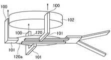
従来、基板の処理面を下方に向けて成膜等を行う場合には、例えば、図4に示すように、機械的なクランプ機構100を用いて基板120を支持し、このクランプ機構100の基板保持部101を上昇させることによって基板120をステージ102にクランプするようにしている。
【0004】
【発明が解決しようとする課題】
しかしながら、このような従来の技術においては、次のような問題があった。
すなわち、真空処理装置内で基板を機械的にクランプする従来技術の場合は、クランプ機構100の基板保持部101が基板120の処理(成膜)面120aに接触せざるを得ないため、特に成膜等の処理を行う場合に、この基板保持部101に付着した成膜材料によってダストが発生するという問題があった。
【0005】
特に、フェイスダウン方式の真空処理装置は、基板120の成膜面120aにおけるダストを低減させる目的で使用される場合が多いため、基板120の成膜面120aに非接触の基板保持技術が要望されていた。
【0006】
さらに、従来の機械的なクランプ機構100を用いる方式では、基板120の温度制御能力及び面内温度分布の均一化の点で十分な結果が得られないため、その向上が望まれていた。
【0007】
本発明は、このような従来の技術の課題を解決するためになされたもので、フェイスダウン方式の真空処理装置において、ダストを発生させることなく基板を保持し、基板の温度制御能力及び面内温度分布の均一性を向上させることを目的とする。
【0008】
【課題を解決するための手段】
上記目的を達成するためになされた請求項1記載の発明は、真空処理槽と、前記真空処理槽内に設けられ、誘電体中に吸着電極を有し且つ鉛直下方側に吸着面を有する静電チャック本体と、前記吸着電極に所定の電圧を印加可能な電源と、前記吸着電極と前記電源との間に流れる電流値を測定する電流測定器とを有する静電吸着装置と、所定の基板を支持可能な基板支持部を有し、該基板支持部が前記静電チャック本体の吸着面に対して接近又は離間できるように構成された基板搬送ロボットと、前記静電チャック本体の吸着面に前記基板を吸着させる際に前記電流測定器にて得られた電流値に基づいて前記基板搬送ロボットの基板支持部の上昇動作を制御するように構成された制御部とを有することを特徴とする真空処理装置である。
【0009】
また、請求項2記載の発明は、請求項1記載の発明において、前記静電吸着装置は、前記静電チャック本体の誘電体中に複数の吸着電極が設けられ、当該吸着電極に対して極性の異なる電圧を印加するように構成されていることを特徴とする。
【0010】
さらに、請求項3記載の発明は、真空処理槽内に請求項1又は2のいずれか1項記載の発明において、基板搬送ロボットの基板支持部に所定の弾性材料からなる支持突部が設けられていることを特徴とする。
【0011】
また、請求項4記載の発明は、請求項1乃至3のいずれか1項記載の真空処理装置において前記静電吸着装置の静電チャック本体の吸着面に基板を吸着保持させる方法であって、前記静電チャック本体の吸着電極に対して所定の電圧を印加した状態において、前記基板搬送ロボットの基板支持部に支持された基板を前記静電チャック本体の吸着面の下方に近接配置し、前記電流測定器によって測定された前記吸着電極及び前記電源間の電流値に基づいて前記基板搬送ロボットの基板支持部の上昇動作を制御することを特徴とする基板保持方法である。
【0012】
一方、請求項5記載の発明は、請求項4記載の発明において、前記電流測定器によって測定された前記吸着電極及び前記電源間の電流値が所定の値を超えたと判断された時点で前記基板搬送ロボットの基板支持部の上昇動作を停止させることを特徴とする。
【0013】
このような構成を有する本発明にあっては、静電吸着装置によって基板を吸着保持させるようにしたことから、フェイスダウン方式の真空処理装置において基板保持部を基板の処理面に接触させずに基板を保持することができ、これによりダストの発生を防止することが可能になる。
【0014】
特に、基板搬送ロボットの基板支持部に所定の弾性材料からなる支持突部を設けるようにすれば、基板搬送時における基板と支持突部との位置ずれを抑制することができるため、これら両者間の摺動に伴うダストの発生を防止することが可能になる。さらに、基板を静電チャック本体の吸着面から離脱させる際に支持突部が基板落下時の振動や衝撃を緩和するため、ダストの発生を防止することが可能になる。
【0015】
したがって、このような本発明によれば、従来の機械的なクランプ機構を用いる方式に比べ、基板の温度制御能力を向上させ、また、面内温度分布を均一化させることが可能になる。
【0016】
【発明の実施の形態】
以下、本発明に係る静電吸着装置及びこれを用いた真空処理装置の実施の形態を図面を参照して詳細に説明する。
図1は、本発明の真空処理装置の一実施の形態の概略構成を示すものである。
図1に示すように、本実施の形態の真空処理装置1は、図示しない真空排気系に接続された真空処理槽2を有し、この真空処理装置1内の上部にステージ3が配設されている。
【0017】
ステージ3には、本発明の一実施の形態としての静電チャック(静電吸着装置)4が固定されている。この静電吸着装置は、誘電体からなる静電チャック本体5を有しており、本実施の形態の場合は、静電チャック本体5の鉛直下方側の面が水平面と平行な吸着面5aとなっている。
【0018】
静電チャック本体5内には、複数(本実施の形態の場合は2つ)の吸着電極6、7が設けられている。ここで、各吸着電極6、7は、それぞれ電流計(電流測定器)8、9を介して直流電源10に接続され、各吸着電極6、7に対して極性の異なる電圧が印加されるように構成されている。
【0019】
図1に示すように、各電流計8、9は、それぞれパーソナルコンピュータ等の制御部11に接続され、各電流計8、9において測定された電流値がこの制御部11において解析されるようになっている。
【0020】
さらに、この制御部11は、所定のシーケンスに基づいて基板搬送ロボット12の動作を制御するように構成されている。
【0021】
基板搬送ロボット12は、基板20を載置可能な支持アーム(基板支持部)13を有している。この支持アーム13は、真空処理槽2に対して出し入れできるように構成され、さらに、上記制御部11からの命令に基づいて昇降できるようになっている。
【0022】
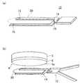
図2(a)は、本実施の形態の基板搬送ロボットの支持アームを示す斜視図、図2(b)は、同基板搬送ロボットの支持アームによって基板20を支持した状態を示す斜視図である。
【0023】
図2(a)(b)に示すように、本実施の形態の支持アーム13は、U字状の腕部14を有している。そして、支持アーム13の腕部14の先端部と基端部とに弾性材料からなる支持突部15が設けられており、この支持突部15によって基板20の縁部を支持するようになっている。
【0024】
本発明の場合、支持突部15の材料としては、例えば、シリコーンゴム等のゴム材料や、ポリ4フッ化エチレン樹脂等のフッ素系の樹脂材料を好適に用いることができる。
【0025】
図3(a)〜(c)は、本実施の形態における基板の吸着方法の一例を示す説明図である。
本実施の形態において基板20を静電チャック4に吸着させる場合には、まず、図1に示すように、支持アーム13によって支持された基板20を真空処理槽2内の静電チャック本体5の直下に配置し、図3(a)に示すように、支持アーム13を上昇させる。この場合、静電チャック4の吸着電極6、7には直流電源10から所定の電圧を印加しておく。
【0026】
次いで、図3(b)に示すように、基板20が静電チャック本体5の吸着面5aに近接した位置(例えば吸着面5aから500μm下方の位置)で支持アーム13の上昇を停止させる。
【0027】
さらに、支持アーム13を微小な速度で例えば段階的に上昇させながら、各電流計8、9に流れる電流値を測定する。
【0028】
そして、制御部11において各電流計8、9に流れる電流値が所定の値を超えたと判断された時点で支持アーム13の上昇を停止させる。
【0029】
その後、図3(c)に示すように、支持アーム13を下降させ、これを真空処理槽2の外に退出させる。
【0030】
このような構成を有する本実施の形態によれば、静電チャック4によって基板20を吸着保持させるようにしたことから、フェイスダウン方式の真空処理装置1において基板保持部を基板20の処理面に接触させずに基板20を保持することができ、これによりダストの発生を防止することができる。
【0031】
特に、本実施の形態にあっては、基板搬送ロボット12の支持アーム13に所定の弾性材料からなる支持突部15を設けるようにしたことから、基板20搬送時における基板20と支持突部15との位置ずれを抑制することができるため、これら両者間の摺動に伴うダストの発生を防止することが可能になる。さらに、基板20を静電チャック本体5の吸着面5aから離脱させる際において支持突部15が基板20落下時の振動や衝撃を緩和するため、ダストの発生を防止することができる。
【0032】
そして、このような本実施の形態の真空処理装置1によれば、従来の機械的なクランプ機構を用いる方式に比べ、基板20の温度制御能力を向上させ、また、面内温度分布を均一化させることができる。
【0033】
なお、本発明は上述の実施の形態に限られることなく、種々の変更を行うことができる。
例えば、上記実施の形態においては、静電チャック本体の吸着面を水平面と平行になるようにしたが、本発明はこれに限られず、静電チャック本体の吸着面を水平面に対して所定の角度だけ傾斜させることも可能である。
【0034】
また、基板搬送ロボットの支持アームの形状、大きさ等は、適宜変更することができる。
【0035】
さらに、基板を静電チャックに吸着させるシーケンスについても、上述した実施の形態のものには限られず、基板の種類やプロセス等に応じて適宜変更が可能である。
【0036】
さらにまた、本発明は、いわゆる単極の吸着電極を有する静電吸着装置においても実現可能であるが、上述した実施の形態のように、複数の吸着電極を有する静電吸着装置を用いれば、プロセスの種類を問わず基板を吸着保持しうる点で特に効果があるものである。
【0037】
加えて、本発明は、例えばシリコンウェハ等の半導体基板のほか、例えばガラス基板等の絶縁性基板等の種々の基板に適用しうるものである。
【0038】
【発明の効果】
以上述べたように本発明によれば、フェイスダウン方式の真空処理装置において、ダストを発生させることなく基板を保持することができる。
また、本発明によれば、基板の温度制御能力を向上させ、また、面内温度分布を均一化させることができる。
【図面の簡単な説明】
【図1】本発明の真空処理装置の一実施の形態の概略構成図
【図2】(a):同実施の形態の基板搬送ロボットの支持アームを示す斜視図
(b):同基板搬送ロボットの支持アームによって基板を支持した状態を示す斜視図
【図3】(a)〜(c):本実施の形態における基板の吸着方法の一例を示す説明図
【図4】従来の機械的なクランプ機構の構成を示す斜視図
【符号の説明】
1…真空処理装置 2…真空処理槽 4…静電チャック(静電吸着装置) 5…静電チャック本体 6、7…吸着電極 8、9…電流計(電流測定器) 10…直流電源 11…制御部 12…基板搬送ロボット 13…支持アーム(基板支持部) 14…腕部 15…支持突部[0001]
BACKGROUND OF THE INVENTION
The present invention relates to a technique of an electrostatic attraction apparatus for adsorbing a processing object in a vacuum processing apparatus.
[0002]
[Prior art]
In a vacuum processing apparatus, when processing such as film formation is performed on a substrate that is a processing target, film formation may be performed with the processing surface of the substrate directed vertically downward (so-called face-down).
[0003]
Conventionally, when film formation or the like is performed with the processing surface of the substrate facing downward, for example, as shown in FIG. 4, the
[0004]
[Problems to be solved by the invention]
However, such a conventional technique has the following problems.
That is, in the case of the conventional technique in which the substrate is mechanically clamped in the vacuum processing apparatus, the
[0005]
In particular, since the face-down type vacuum processing apparatus is often used for the purpose of reducing dust on the
[0006]
Furthermore, the conventional method using the
[0007]
The present invention has been made to solve the above-described problems of the conventional technology. In a face-down type vacuum processing apparatus, the substrate is held without generating dust, and the temperature control capability and in-plane of the substrate are maintained. The object is to improve the uniformity of the temperature distribution.
[0008]
[Means for Solving the Problems]
In order to achieve the above-mentioned object, the invention according to
[0009]
The invention according to
[0010]
Further, in the invention described in
[0011]
The invention according to
[0012]
On the other hand, the invention according to
[0013]
In the present invention having such a configuration, since the substrate is sucked and held by the electrostatic chucking device, the substrate holding unit is not brought into contact with the processing surface of the substrate in the face-down type vacuum processing device. It is possible to hold the substrate, thereby preventing dust generation.
[0014]
In particular, if a support protrusion made of a predetermined elastic material is provided on the substrate support portion of the substrate transfer robot, positional deviation between the substrate and the support protrusion during substrate transfer can be suppressed. It is possible to prevent the generation of dust associated with the sliding of. In addition, when the substrate is detached from the attracting surface of the electrostatic chuck body, the support projections reduce vibrations and shocks when the substrate is dropped, so that generation of dust can be prevented.
[0015]
Therefore, according to the present invention, the temperature control ability of the substrate can be improved and the in-plane temperature distribution can be made uniform as compared with the conventional method using a mechanical clamping mechanism.
[0016]
DETAILED DESCRIPTION OF THE INVENTION
DESCRIPTION OF EMBODIMENTS Hereinafter, embodiments of an electrostatic adsorption device and a vacuum processing apparatus using the same according to the present invention will be described in detail with reference to the drawings.
FIG. 1 shows a schematic configuration of an embodiment of a vacuum processing apparatus of the present invention.
As shown in FIG. 1, a
[0017]
An electrostatic chuck (electrostatic chuck) 4 as an embodiment of the present invention is fixed to the
[0018]
In the
[0019]
As shown in FIG. 1, each ammeter 8, 9 is connected to a
[0020]
Further, the
[0021]
The
[0022]
FIG. 2A is a perspective view showing a support arm of the substrate transfer robot of the present embodiment, and FIG. 2B is a perspective view showing a state in which the
[0023]
As shown in FIGS. 2A and 2B, the
[0024]
In the case of the present invention, as the material of the
[0025]
FIGS. 3A to 3C are explanatory views showing an example of a substrate adsorption method in the present embodiment.
In the case where the
[0026]
Next, as shown in FIG. 3B, the raising of the
[0027]
Further, the value of the current flowing through each ammeter 8 and 9 is measured while raising the
[0028]
Then, when the
[0029]
Thereafter, as shown in FIG. 3 (c), the
[0030]
According to the present embodiment having such a configuration, the
[0031]
In particular, in the present embodiment, since the
[0032]
And according to such a
[0033]
The present invention is not limited to the above-described embodiment, and various changes can be made.
For example, in the above-described embodiment, the suction surface of the electrostatic chuck body is parallel to the horizontal plane. However, the present invention is not limited to this, and the suction surface of the electrostatic chuck body is at a predetermined angle with respect to the horizontal plane. It is also possible to tilt only.
[0034]
Further, the shape, size, etc. of the support arm of the substrate transfer robot can be changed as appropriate.
[0035]
Further, the sequence for attracting the substrate to the electrostatic chuck is not limited to the one in the above-described embodiment, and can be appropriately changed according to the type of substrate, process, and the like.
[0036]
Furthermore, the present invention can be realized in an electrostatic adsorption apparatus having a so-called unipolar adsorption electrode, but if an electrostatic adsorption apparatus having a plurality of adsorption electrodes is used as in the above-described embodiment, This is particularly effective in that the substrate can be adsorbed and held regardless of the type of process.
[0037]
In addition, the present invention can be applied to various substrates such as an insulating substrate such as a glass substrate in addition to a semiconductor substrate such as a silicon wafer.
[0038]
【The invention's effect】
As described above, according to the present invention, the substrate can be held without generating dust in the face-down type vacuum processing apparatus.
Further, according to the present invention, the temperature control ability of the substrate can be improved and the in-plane temperature distribution can be made uniform.
[Brief description of the drawings]
FIG. 1 is a schematic configuration diagram of an embodiment of a vacuum processing apparatus of the present invention. FIG. 2A is a perspective view showing a support arm of a substrate transfer robot of the embodiment. FIG. FIG. 3 is a perspective view showing a state in which a substrate is supported by a support arm of FIG. 3 (a) to (c): an explanatory view showing an example of a substrate adsorption method in the present embodiment. FIG. Perspective view showing the structure of the mechanism
DESCRIPTION OF
Claims (5)
Translated fromJapanese前記真空処理槽内に設けられ、誘電体中に吸着電極を有し且つ鉛直下方側に吸着面を有する静電チャック本体と、前記吸着電極に所定の電圧を印加可能な電源と、前記吸着電極と前記電源との間に流れる電流値を測定する電流測定器とを有する静電吸着装置と、
所定の基板を支持可能な基板支持部を有し、該基板支持部が前記静電チャック本体の吸着面に対して接近又は離間できるように構成された基板搬送ロボットと、
前記静電チャック本体の吸着面に前記基板を吸着させる際に前記電流測定器にて得られた電流値に基づいて前記基板搬送ロボットの基板支持部の上昇動作を制御するように構成された制御部とを有することを特徴とする真空処理装置。A vacuum treatment tank;
An electrostatic chuck body provided in the vacuum processing tank, having an adsorption electrode in a dielectric and having an adsorption surface on a vertically lower side, a power source capable of applying a predetermined voltage to the adsorption electrode, and the adsorption electrode And an electrostatic adsorption device having a current measuring device for measuring a current value flowing between the power source and the power source;
A substrate transport robot having a substrate support portion capable of supporting a predetermined substrate, the substrate support portion configured to be close to or away from the attracting surface of the electrostatic chuck body;
A control configured to control the ascending operation of the substrate support portion of the substrate transfer robot based on the current value obtained by the current measuring device when the substrate is attracted to the attracting surface of the electrostatic chuck body. the vacuum processingapparatus characterized byhaving a part.
前記静電チャック本体の吸着電極に対して所定の電圧を印加した状態において、前記基板搬送ロボットの基板支持部に支持された基板を前記静電チャック本体の吸着面の下方に近接配置し、
前記電流測定器によって測定された前記吸着電極及び前記電源間の電流値に基づいて前記基板搬送ロボットの基板支持部の上昇動作を制御することを特徴とする基板保持方法。The vacuum processing apparatus according toany one of claims1 to 3 ,wherein the substrate isattracted and held onthe attracting surface of the electrostatic chuck body of the electrostatic attracting apparatus .
In a state where a predetermined voltage is applied to the chucking electrode of the electrostatic chuck body, thesubstrate supported by thesubstrate support part of the substrate transport robot is disposed close tothe lower surfaceof the chucking surfaceof the electrostatic chuck body,
Substrate holding method, characterized in that saidcontrolling the upward movement of thesubstrate support portion of the substrate transport robot based on the current value between the measured the suction electrode andthe power source by the current measuring device.
Priority Applications (1)
| Application Number | Priority Date | Filing Date | Title |
|---|---|---|---|
| JP2000112903AJP4489904B2 (en) | 2000-04-14 | 2000-04-14 | Vacuum processing apparatus and substrate holding method |
Applications Claiming Priority (1)
| Application Number | Priority Date | Filing Date | Title |
|---|---|---|---|
| JP2000112903AJP4489904B2 (en) | 2000-04-14 | 2000-04-14 | Vacuum processing apparatus and substrate holding method |
Publications (2)
| Publication Number | Publication Date |
|---|---|
| JP2001298072A JP2001298072A (en) | 2001-10-26 |
| JP4489904B2true JP4489904B2 (en) | 2010-06-23 |
Family
ID=18624970
Family Applications (1)
| Application Number | Title | Priority Date | Filing Date |
|---|---|---|---|
| JP2000112903AExpired - LifetimeJP4489904B2 (en) | 2000-04-14 | 2000-04-14 | Vacuum processing apparatus and substrate holding method |
Country Status (1)
| Country | Link |
|---|---|
| JP (1) | JP4489904B2 (en) |
Families Citing this family (43)
| Publication number | Priority date | Publication date | Assignee | Title |
|---|---|---|---|---|
| JP4603099B2 (en) | 2008-06-20 | 2010-12-22 | キヤノンアネルバ株式会社 | Vacuum processing apparatus, vacuum processing method, and electronic device manufacturing method |
| US8518204B2 (en) | 2011-11-18 | 2013-08-27 | LuxVue Technology Corporation | Method of fabricating and transferring a micro device and an array of micro devices utilizing an intermediate electrically conductive bonding layer |
| US8573469B2 (en) | 2011-11-18 | 2013-11-05 | LuxVue Technology Corporation | Method of forming a micro LED structure and array of micro LED structures with an electrically insulating layer |
| US8333860B1 (en)* | 2011-11-18 | 2012-12-18 | LuxVue Technology Corporation | Method of transferring a micro device |
| US8794501B2 (en) | 2011-11-18 | 2014-08-05 | LuxVue Technology Corporation | Method of transferring a light emitting diode |
| US8349116B1 (en) | 2011-11-18 | 2013-01-08 | LuxVue Technology Corporation | Micro device transfer head heater assembly and method of transferring a micro device |
| US9773750B2 (en) | 2012-02-09 | 2017-09-26 | Apple Inc. | Method of transferring and bonding an array of micro devices |
| US9548332B2 (en) | 2012-04-27 | 2017-01-17 | Apple Inc. | Method of forming a micro LED device with self-aligned metallization stack |
| US9105492B2 (en) | 2012-05-08 | 2015-08-11 | LuxVue Technology Corporation | Compliant micro device transfer head |
| US8415768B1 (en) | 2012-07-06 | 2013-04-09 | LuxVue Technology Corporation | Compliant monopolar micro device transfer head with silicon electrode |
| US8791530B2 (en) | 2012-09-06 | 2014-07-29 | LuxVue Technology Corporation | Compliant micro device transfer head with integrated electrode leads |
| US9162880B2 (en) | 2012-09-07 | 2015-10-20 | LuxVue Technology Corporation | Mass transfer tool |
| US9558721B2 (en) | 2012-10-15 | 2017-01-31 | Apple Inc. | Content-based adaptive refresh schemes for low-power displays |
| US9236815B2 (en) | 2012-12-10 | 2016-01-12 | LuxVue Technology Corporation | Compliant micro device transfer head array with metal electrodes |
| US9217541B2 (en) | 2013-05-14 | 2015-12-22 | LuxVue Technology Corporation | Stabilization structure including shear release posts |
| US9484504B2 (en) | 2013-05-14 | 2016-11-01 | Apple Inc. | Micro LED with wavelength conversion layer |
| US9136161B2 (en) | 2013-06-04 | 2015-09-15 | LuxVue Technology Corporation | Micro pick up array with compliant contact |
| US8987765B2 (en) | 2013-06-17 | 2015-03-24 | LuxVue Technology Corporation | Reflective bank structure and method for integrating a light emitting device |
| US9111464B2 (en) | 2013-06-18 | 2015-08-18 | LuxVue Technology Corporation | LED display with wavelength conversion layer |
| US8928021B1 (en) | 2013-06-18 | 2015-01-06 | LuxVue Technology Corporation | LED light pipe |
| US9035279B2 (en) | 2013-07-08 | 2015-05-19 | LuxVue Technology Corporation | Micro device with stabilization post |
| US9296111B2 (en) | 2013-07-22 | 2016-03-29 | LuxVue Technology Corporation | Micro pick up array alignment encoder |
| US9087764B2 (en) | 2013-07-26 | 2015-07-21 | LuxVue Technology Corporation | Adhesive wafer bonding with controlled thickness variation |
| US9153548B2 (en) | 2013-09-16 | 2015-10-06 | Lux Vue Technology Corporation | Adhesive wafer bonding with sacrificial spacers for controlled thickness variation |
| US9367094B2 (en) | 2013-12-17 | 2016-06-14 | Apple Inc. | Display module and system applications |
| US9768345B2 (en) | 2013-12-20 | 2017-09-19 | Apple Inc. | LED with current injection confinement trench |
| US9583466B2 (en) | 2013-12-27 | 2017-02-28 | Apple Inc. | Etch removal of current distribution layer for LED current confinement |
| US9450147B2 (en) | 2013-12-27 | 2016-09-20 | Apple Inc. | LED with internally confined current injection area |
| US9542638B2 (en) | 2014-02-18 | 2017-01-10 | Apple Inc. | RFID tag and micro chip integration design |
| US9583533B2 (en) | 2014-03-13 | 2017-02-28 | Apple Inc. | LED device with embedded nanowire LEDs |
| JP6024698B2 (en)* | 2014-04-08 | 2016-11-16 | ウシオ電機株式会社 | Vacuum suction arm for substrate transfer |
| US9522468B2 (en) | 2014-05-08 | 2016-12-20 | Apple Inc. | Mass transfer tool manipulator assembly with remote center of compliance |
| US9318475B2 (en) | 2014-05-15 | 2016-04-19 | LuxVue Technology Corporation | Flexible display and method of formation with sacrificial release layer |
| US9741286B2 (en) | 2014-06-03 | 2017-08-22 | Apple Inc. | Interactive display panel with emitting and sensing diodes |
| US9624100B2 (en) | 2014-06-12 | 2017-04-18 | Apple Inc. | Micro pick up array pivot mount with integrated strain sensing elements |
| US9570002B2 (en) | 2014-06-17 | 2017-02-14 | Apple Inc. | Interactive display panel with IR diodes |
| US9425151B2 (en) | 2014-06-17 | 2016-08-23 | Apple Inc. | Compliant electrostatic transfer head with spring support layer |
| US9828244B2 (en) | 2014-09-30 | 2017-11-28 | Apple Inc. | Compliant electrostatic transfer head with defined cavity |
| US9705432B2 (en) | 2014-09-30 | 2017-07-11 | Apple Inc. | Micro pick up array pivot mount design for strain amplification |
| US9478583B2 (en) | 2014-12-08 | 2016-10-25 | Apple Inc. | Wearable display having an array of LEDs on a conformable silicon substrate |
| JP2018181969A (en)* | 2017-04-07 | 2018-11-15 | 株式会社 天谷製作所 | Processing unit |
| JP6434558B2 (en)* | 2017-04-07 | 2018-12-05 | 株式会社 天谷製作所 | Processing equipment |
| KR102251891B1 (en)* | 2020-12-08 | 2021-05-13 | 주식회사 기가레인 | Apparatus for supporting substrate and method for transferring substrate using the same |
Family Cites Families (4)
| Publication number | Priority date | Publication date | Assignee | Title |
|---|---|---|---|---|
| JP2510290B2 (en)* | 1989-07-24 | 1996-06-26 | 富士電機株式会社 | How to remove the object to be processed from the electrostatic chuck |
| JPH10303287A (en)* | 1997-04-25 | 1998-11-13 | Mitsubishi Electric Corp | Electrostatic chuck device and semiconductor device |
| JP3913355B2 (en)* | 1997-05-23 | 2007-05-09 | 株式会社アルバック | Processing method |
| JP4169839B2 (en)* | 1998-09-08 | 2008-10-22 | 株式会社アルバック | Vacuum processing apparatus and vacuum processing method |
- 2000
- 2000-04-14JPJP2000112903Apatent/JP4489904B2/ennot_activeExpired - Lifetime
Also Published As
| Publication number | Publication date |
|---|---|
| JP2001298072A (en) | 2001-10-26 |
Similar Documents
| Publication | Publication Date | Title |
|---|---|---|
| JP4489904B2 (en) | Vacuum processing apparatus and substrate holding method | |
| CN101663745B (en) | Apparatus for transferring a wafer | |
| KR101202559B1 (en) | Apparatus for removing foreign material from substrate and method for removing foreign material from substrate | |
| JP4467720B2 (en) | Substrate transfer device | |
| KR101400453B1 (en) | Substrate conveyance method and substrate conveyance system | |
| US4733632A (en) | Wafer feeding apparatus | |
| CN112335031B (en) | Power supply device for electrostatic chuck and substrate management method | |
| JP6066861B2 (en) | Substrate cleaning apparatus, substrate back surface cleaning method and cleaning mechanism | |
| US6185085B1 (en) | System for transporting and electrostatically chucking a semiconductor wafer or the like | |
| TWI309223B (en) | Substrate transfer apparatus | |
| JP6851202B2 (en) | Board holder, vertical board transfer device and board processing device | |
| JP2021168370A (en) | How to mount the substrate support, plasma processing system and edge ring | |
| KR950034663A (en) | Wafer Transfer Device and Method | |
| KR102493572B1 (en) | Apparatus for treating substrate and method for guiding location | |
| JP2022002262A (en) | Plasma processing system, plasma processing apparatus, and method for replacing edge ring | |
| JP2020155598A (en) | Electrostatic chuck | |
| JP4188144B2 (en) | Electrostatic holding device, electrostatic tweezers using the same, and conveying device | |
| JP4490524B2 (en) | Electrostatic adsorption stage and substrate processing apparatus | |
| JPH11145266A (en) | Apparatus and method of electrostatic chucking, and apparatus and method of transferring substrate using the same | |
| TWI257913B (en) | Vacuum chuck | |
| JP2919837B2 (en) | Wafer carrier | |
| JP3123956B2 (en) | Electrostatic suction device and electron beam lithography device using the same | |
| JP2006273447A (en) | Substrate adsorption method and apparatus | |
| JPH06291174A (en) | Electrostatic chuck, and method for adhering and holding semiconductor wafer to electrostatic chuck | |
| JP2004031487A (en) | Electrostatic attracting device and vacuum treating device using the same |
Legal Events
| Date | Code | Title | Description |
|---|---|---|---|
| A621 | Written request for application examination | Free format text:JAPANESE INTERMEDIATE CODE: A621 Effective date:20070219 | |
| A977 | Report on retrieval | Free format text:JAPANESE INTERMEDIATE CODE: A971007 Effective date:20090722 | |
| A131 | Notification of reasons for refusal | Free format text:JAPANESE INTERMEDIATE CODE: A131 Effective date:20090728 | |
| A521 | Request for written amendment filed | Free format text:JAPANESE INTERMEDIATE CODE: A523 Effective date:20090928 Free format text:JAPANESE INTERMEDIATE CODE: A821 Effective date:20090928 | |
| TRDD | Decision of grant or rejection written | ||
| A01 | Written decision to grant a patent or to grant a registration (utility model) | Free format text:JAPANESE INTERMEDIATE CODE: A01 Effective date:20100330 | |
| A01 | Written decision to grant a patent or to grant a registration (utility model) | Free format text:JAPANESE INTERMEDIATE CODE: A01 | |
| A61 | First payment of annual fees (during grant procedure) | Free format text:JAPANESE INTERMEDIATE CODE: A61 Effective date:20100401 | |
| FPAY | Renewal fee payment (event date is renewal date of database) | Free format text:PAYMENT UNTIL: 20130409 Year of fee payment:3 | |
| R150 | Certificate of patent or registration of utility model | Free format text:JAPANESE INTERMEDIATE CODE: R150 | |
| FPAY | Renewal fee payment (event date is renewal date of database) | Free format text:PAYMENT UNTIL: 20130409 Year of fee payment:3 | |
| FPAY | Renewal fee payment (event date is renewal date of database) | Free format text:PAYMENT UNTIL: 20160409 Year of fee payment:6 | |
| R250 | Receipt of annual fees | Free format text:JAPANESE INTERMEDIATE CODE: R250 | |
| R250 | Receipt of annual fees | Free format text:JAPANESE INTERMEDIATE CODE: R250 | |
| R250 | Receipt of annual fees | Free format text:JAPANESE INTERMEDIATE CODE: R250 | |
| R250 | Receipt of annual fees | Free format text:JAPANESE INTERMEDIATE CODE: R250 |