JP4489359B2 - Nonvolatile semiconductor memory device - Google Patents
Nonvolatile semiconductor memory deviceDownload PDFInfo
- Publication number
- JP4489359B2 JP4489359B2JP2003023690AJP2003023690AJP4489359B2JP 4489359 B2JP4489359 B2JP 4489359B2JP 2003023690 AJP2003023690 AJP 2003023690AJP 2003023690 AJP2003023690 AJP 2003023690AJP 4489359 B2JP4489359 B2JP 4489359B2
- Authority
- JP
- Japan
- Prior art keywords
- film
- insulating film
- silicon oxynitride
- gate electrode
- oxynitride film
- Prior art date
- Legal status (The legal status is an assumption and is not a legal conclusion. Google has not performed a legal analysis and makes no representation as to the accuracy of the status listed.)
- Expired - Fee Related
Links
Images


Classifications
- H—ELECTRICITY
- H10—SEMICONDUCTOR DEVICES; ELECTRIC SOLID-STATE DEVICES NOT OTHERWISE PROVIDED FOR
- H10D—INORGANIC ELECTRIC SEMICONDUCTOR DEVICES
- H10D30/00—Field-effect transistors [FET]
- H10D30/01—Manufacture or treatment
- H10D30/021—Manufacture or treatment of FETs having insulated gates [IGFET]
- H10D30/0413—Manufacture or treatment of FETs having insulated gates [IGFET] of FETs having charge-trapping gate insulators, e.g. MNOS transistors
- H—ELECTRICITY
- H10—SEMICONDUCTOR DEVICES; ELECTRIC SOLID-STATE DEVICES NOT OTHERWISE PROVIDED FOR
- H10D—INORGANIC ELECTRIC SEMICONDUCTOR DEVICES
- H10D30/00—Field-effect transistors [FET]
- H10D30/60—Insulated-gate field-effect transistors [IGFET]
- H10D30/69—IGFETs having charge trapping gate insulators, e.g. MNOS transistors
- H—ELECTRICITY
- H10—SEMICONDUCTOR DEVICES; ELECTRIC SOLID-STATE DEVICES NOT OTHERWISE PROVIDED FOR
- H10D—INORGANIC ELECTRIC SEMICONDUCTOR DEVICES
- H10D64/00—Electrodes of devices having potential barriers
- H10D64/01—Manufacture or treatment
- H10D64/031—Manufacture or treatment of data-storage electrodes
- H10D64/037—Manufacture or treatment of data-storage electrodes comprising charge-trapping insulators
- G—PHYSICS
- G11—INFORMATION STORAGE
- G11C—STATIC STORES
- G11C16/00—Erasable programmable read-only memories
- G11C16/02—Erasable programmable read-only memories electrically programmable
- G11C16/04—Erasable programmable read-only memories electrically programmable using variable threshold transistors, e.g. FAMOS
- G11C16/0466—Erasable programmable read-only memories electrically programmable using variable threshold transistors, e.g. FAMOS comprising cells with charge storage in an insulating layer, e.g. metal-nitride-oxide-silicon [MNOS], silicon-oxide-nitride-oxide-silicon [SONOS]
Landscapes
- Non-Volatile Memory (AREA)
- Semiconductor Memories (AREA)
Description
Translated fromJapanese【0001】
【発明の属する技術分野】
本発明は不揮発性半導体記憶装置に係り、特に低電圧、高速プログラミングが可能な高信頼性の不揮発性半導体記憶装置に関する。
【0002】
【従来の技術】
絶縁膜を記憶ノードとする不揮発性メモリ(不揮発性半導体記憶装置)の代表的な例としてMNOS(Metal-Nitride-Oxide-Semiconductor)メモリ、MONOS(Metal-Oxide-Nitride-Oxide-Semiconductor)メモリが挙げられる。MNOSメモリは、導電性ゲート電極(M)、シリコン窒化膜(N、以下「Si窒化膜」という)、シリコン酸化膜(O、以下「Si酸化膜」という)および半導体基板(S)の積層構造からなり、MONOSメモリは、導電性ゲート電極(M)、Si酸化膜(O)、Si窒化膜(N)、Si酸化膜(O)および半導体基板(S)の積層構造からなる。両者ともに電荷保持機能を有するSi窒化膜にキャリアを注入、放出することで情報を記憶する。
【0003】
上記不揮発性メモリの構造やプログラム方法については、例えば、特許文献1(特開2001−102466号公報(対応USP6,255,166号))、特許文献2(特開2001−148434号公報)および特許文献3(USP5,969,383号公報)等に開示されている。
【0004】
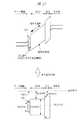
以下、特許文献1(特開2001−102466号公報)および特許文献2(特開2001−148434号公報)に開示されているタイプのメモリセルの構造と動作を図7を用いて簡単に説明する。
【0005】
この不揮発性メモリは、記憶部を構成するメモリMOS型トランジスタと、そのメモリ部を選択して情報を読み出すための選択MOS型トランジスタの2つのMOS型トランジスタから構成されている。選択MOS型トランジスタの拡散層(ソース領域)607Bはビット線に、選択ゲート電極603は制御ゲート配線に接続されている。一方、メモリMOS型トランジスタの拡散層(ドレイン領域)607Aは共通線に、メモリゲート電極605はワード線に接続されている。
【0006】
メモリMOS型トランジスタの容量絶縁膜604は3層膜で構成されており、例えばシリコン基板(以下、「Si基板」という)601表面側から、Si酸化膜(第1層膜)604a、Si窒化膜(第2層膜)604bおよびSi酸化膜(第3層膜)604cで構成されている。膜厚は、第1層膜604aが3〜4nm程度、第2層膜604bが10nm以下、第3層膜604cが2〜4nm程度である。
【0007】
上記メモリMOS型トランジスタの第2層膜604bであるSi窒化膜は、キャリア保持機能を有する電荷保持絶縁膜であり、Si窒化膜中とその上下の界面に形成されたトラップ準位にキャリアを捕獲する。電荷保持膜としては、例えばSi窒化膜、Si酸窒化膜もしくは酸化タンタル等が用いられる。第1層膜604aおよび第3層膜604cは電位障壁膜であり、例えばSi酸化膜やSi酸窒化膜が用いられる。
【0008】
書込み動作は、選択MOS型トランジスタの拡散層(ソース領域)607Bおよびそのゲート電極603に所定の電圧を印加して選択MOS型トランジスタをオン状態にすると同時に、メモリMOS型トランジスタの拡散層(ドレイン領域)607Aおよびそのゲート電極605に所定の電圧を印加する。この時、Si基板表面のキャリアの一部がメモリMOS型トランジスタのゲート電界により容量絶縁膜604に注入される。注入されたキャリアは第1層膜であるSi酸化膜604aの電位障壁を超えて第2層膜であるSi窒化膜604bに捕獲される。
【0009】
消去動作は2つに大別される。1つはメモリMOS型トランジスタの電荷保持膜であるSi窒化膜604bから、その下層の電位障壁膜であるSi酸化膜604aを介してSi基板601側にキャリアを引き抜く方法、もう1つは第3層膜であるSi酸化膜604cを介してメモリMOS型トランジスタのゲート電極605に引き抜く方法である。両方法ともにメモリMOS型トランジスタのゲート電極605に電圧を印加することでSi窒化膜604bからキャリアを引き抜いて消去を行う。しかし、書込み動作と同じ極性(メモリゲート電極の印加電圧)を用いて消去できる後者の方法は、回路構成が容易でチップ面積も小さくできる利点がある。
【0010】
読み出し動作は、選択MOS型トランジスタをオン状態にした時、メモリMOS型トランジスタのしきい値電圧の状態により、所定の電流が流れるか否かに応じて記憶情報を読み出す。
【0011】
次に、特許文献3(USP5,969,383号公報)に開示されているタイプのメモリセルの構造と動作を、図8を用いて簡単に説明する。
【0012】
この不揮発性メモリも、記憶部を構成するメモリMOS型トランジスタと、そのメモリ部を選択して情報を読み出すための選択MOS型トランジスタの2つのMOS型トランジスタから構成されている。選択MOS型トランジスタの拡散層(ソース領域)707Bはビット線に、選択ゲート電極703は制御ゲート配線に接続されている。一方、メモリMOS型トランジスタの拡散層(ドレイン領域)707Aは共通線に、メモリゲート電極705はワード線に接続されている。
【0013】
メモリMOS型トランジスタの容量絶縁膜704は3層膜で構成されており、例えばSi基板701の表面側から、Si酸化膜(第1層膜)704a、Si窒化膜(第2層膜)704bおよびSi酸化膜(第3層膜)704cで構成されている。膜厚は、第1層膜704aが5〜15nm、第2層膜704bが5〜15nm、第3層膜704cが5〜15nm程度である。709は、絶縁膜である。
【0014】
書込み動作は、選択MOS型トランジスタの拡散層(ソース領域)707Bおよびそのゲート電極703に所定の電圧を印加して選択MOS型トランジスタをオン状態にすると同時に、メモリMOS型トランジスタの拡散層(ドレイン領域)707Aおよびそのゲート電極705に所定の電圧を印加する。例えば、ソース領域707Bに0V、選択MOS型トランジスタのゲート電極703に1〜2V、ドレイン領域707Aに3〜5V、メモリMOS型トランジスタのゲート電極703に8〜10Vの電圧を印加して容量絶縁膜の一部であるSi窒化膜704bに電子を注入する。
【0015】
消去動作は、メモリMOS型トランジスタのメモリゲート電極705に負バイアス、その拡散層707Aに正バイアスを印加し、バンド間トンネリングを用いてホットホールを電荷保持膜に注入する方式で行う。例えば、ドレイン領域707Aに5〜7V、メモリMOS型トランジスタのゲート電極705に−9〜−11V、ソース領域707Bと選択MOS型トランジスタのゲート電極703を0Vもしくはオープン状態として消去を行う。
【0016】
読み出し動作は、選択MOS型トランジスタをオン状態にした時、メモリMOS型トランジスタのしきい値電圧の状態により、所定の電流が流れるか否かに応じて記憶情報を読み出す。
【0017】
【特許文献1】
特開2001−102466号公報(対応USP6,255,166号)
【0018】
【特許文献2】
特開2001−148434号公報
【0019】
【特許文献3】
USP5,969,383号公報
【0020】
【発明が解決しようとする課題】
本発明者らは、不揮発性半導体記憶装置の研究・開発に従事しており、装置の高性能化に関する種々の検討を行っている。
【0021】
例えば、書込みや消去の速度の高速化、書込みや消去に伴う電流駆動能力Gm劣化の抑制、及び電荷保持特性の向上等を図るための装置の構造、また、高速書込みや高速消去の方法等を検討している。
【0022】
中でも、追って詳細に説明する本発明者らの検討の結果、電荷保持絶縁膜としてSi酸窒化膜を用いることで書込みや消去が高速化し、また、電荷保持特性が向上することが判明した。
【0023】
なお、特許文献1等には、キャリア捕獲機能を有する第2層として、例えば、シリコン酸化膜、酸化タンタル膜または第1、第3層より酸素含有率の少ないシリコン酸化窒化膜を用いることが記載されているが、Si酸窒化膜の特性についての詳細な検討はなされていない。
【0024】
また、さらに検討を進めた結果、電荷保持絶縁膜としてSi酸窒化膜を用いた場合、上記特性の向上が図れる一方、電流駆動能力Gmが劣化することが判明した。なお、この電流駆動能力Gmの劣化についても追って詳細に説明する。
【0025】
本発明の目的は、不揮発性半導体記憶装置の性能の向上を図ることにある。
【0026】
特に、電荷保持特性の向上を図ることにある。また、電流駆動能力の劣化を防止することにある。また、動作速度の向上を図ることにある。
【0027】
本発明の前記ならびにその他の目的と新規な特徴は、本明細書の記述および添付図面から明らかになるであろう。
【0028】
【課題を解決するための手段】
本願において開示される発明のうち、代表的なものの概要を簡単に説明すれば、次のとおりである。
【0029】
本発明の不揮発性半導体記憶装置は、(a)半導体基板中に形成された第1および第2半導体領域と、(b)前記第1および第2半導体領域間上の前記半導体基板の上部に形成された第1導電体および第2導電体と、(c)前記第1導電体と前記半導体基板との間に形成された第1絶縁膜と、(d)前記第2導電体と前記半導体基板との間に形成された第2絶縁膜と、を有し、(e)前記第2絶縁膜は、前記半導体基板上の電位障壁膜と、その上部のシリコン酸窒化膜よりなり、前記シリコン酸窒化膜上には前記第2導電体が位置するものである。
【0030】
また、本発明の不揮発性半導体記憶装置は、(a)半導体基板中に形成された第1および第2半導体領域と、(b)前記第1および第2半導体領域間上の前記半導体基板の上部に形成された第1導電体および第2導電体と、(c)前記第1導電体と前記半導体基板との間に形成された第1絶縁膜と、(d)前記第2導電体と前記半導体基板との間に形成された第2絶縁膜と、を有し、(e)前記第2絶縁膜は、前記半導体基板上の電位障壁膜と、その上部の電荷保持膜よりなり、前記電荷保持膜は、シリコン酸窒化膜と、真空準位から当該膜の伝導体までのエネルギーと、当該膜のバンドギャップとの和が、前記シリコン酸窒化膜より小さい第3絶縁膜とを有し、前記シリコン酸窒化膜の電荷トラップ密度と膜厚の積は、前記第3絶縁膜の電荷トラップ密度と膜厚の積より大きいものである。
【0031】
また、本発明の不揮発性半導体記憶装置は、(a)半導体基板中に形成された第1および第2半導体領域と、(b)前記第1および第2半導体領域間上の前記半導体基板の上部に形成された第1導電体および第2導電体と、(c)前記第1導電体と前記半導体基板との間に形成された第1絶縁膜と、(d)前記第2導電体と前記半導体基板との間に形成された第2絶縁膜と、を有し、(e)前記第2絶縁膜は、前記半導体基板上の第1電位障壁膜、その上部のシリコン酸窒化膜およびその上部の第2電位障壁膜よりなり、(f)前記シリコン酸窒化膜は、電荷保持機能を有し、前記シリコン酸窒化膜に蓄積された電子は、前記半導体基板側から正孔を注入することにより消去されるものである。
【0032】
【発明の実施の形態】
以下、本発明の実施の形態を図面に基づいて詳細に説明する。なお、実施の形態を説明するための全図において同一機能を有するものは同一の符号を付し、その繰り返しの説明は省略する。
【0033】
(実施の形態1)
本実施の形態を説明する前に、本発明者らがあらかじめ検討した事項について説明する。
【0034】
まず、本発明者らは、メモリMOS型トランジスタの電荷保持膜の膜種をパラメータとして書込み/消去特性、読み出し特性および電荷保持特性の関係について検討した。
【0035】
図9に本検討に用いたメモリセル(不揮発性半導体記憶装置、フラッシュメモリ)の構造の断面図を示す。基本的な素子構造は図7に示したメモリセルと同様であるが、選択MOS型トランジスタの選択ゲート電極803がメモリMOS型トランジスタのメモリゲート電極805に乗り上げている点で異なっている。メモリMOS型トランジスタの容量絶縁膜804の構成は、Si基板801側より下層電位障壁膜、電荷保持膜および上層電位障壁膜の3層構造となっている。
【0036】
情報の書込みは、選択MOS型トランジスタで発生させたチャネル部のホットエレクトロンをメモリMOS型トランジスタの容量絶縁膜804の一部である電荷保持膜へ、所定のしきい値になるまで注入する方式で行った。このような書込み方式は、ホットエレクトロン注入方式と呼ばれる。中でも、ソース側からホットエレクトロンを注入する場合には、ソースサイド・インジェクション方式と呼ばれる。
【0037】
消去は、メモリMOS型トランジスタのゲート電極805へ、正の電圧を所定のしきい値になるまで印加する方式で行った。この場合、電荷保持膜中の電子は、メ
モリゲート電極へ引き抜かれる。
【0038】
電荷保持特性は、(ステップ1)所定のしきい値になるまで書込みを行い、次いで、(ステップ2)メモリMOS型トランジスタのゲート電極に1.8Vの電圧を印加し、85℃で10万秒放置した後、(ステップ3)書込み直後と高温放置後のしきい値を比較する方法で評価した。
【0039】
電荷保持膜の膜種として、Si窒化膜、Si酸窒化膜、酸化タンタル膜および酸化アルミニウム膜(アルミナ膜)について検討した。電荷保持膜の上下の電位障壁膜としては、Si酸化膜を用いた。下層の電位障壁膜は、4nm、上層の電位障壁膜は1.8nmとした。
【0040】
書込み特性の評価では、電荷保持膜としてSi窒化膜およびSi酸窒化膜を用いた場合は、所定の時間内に書込みが終了した。これに対し、酸化タンタル膜、アルミナ膜を用いた場合には、所定の時間内に書込みが出来なかった。特に、酸化タンタル膜を用いた場合は、長時間書込みを行なっても、所定のしきい値までには到達しなかった。これは、酸化タンタル膜やアルミナ膜が、Si窒化膜やSi酸窒化膜に比べ電子のトラップ準位密度が小さいためと考えられる。しかしながら、アルミナ膜を用いた場合、消去特性や電荷保持特性は良好であるので、高速書込みを要求しない不揮発性メモリの電荷保持膜としてアルミナ膜を用いることは充分可能である。
【0041】
一方、消去特性および電荷保持特性の評価において、電荷保持膜としてSi酸窒化膜を用いた方が、Si窒化膜を用いた場合に比べ、消去速度が高速化すること、および優れた電荷保持特性を示すことを新たに見出した。また、電荷保持膜をSi酸窒化膜とSi窒化膜の組み合わせで積層構造としても同様の効果が得られた。但し、Si酸窒化膜の膜厚がSi窒化膜よりも厚い場合、すなわちSi酸窒化膜の電荷保持量がSi窒化膜のそれに比べ大きい場合に限られた。
【0042】
電荷保持膜としてSi酸窒化膜を用いた方が、消去速度が高速化することは、Si窒化膜とSi酸窒化膜の電流―電圧特性から以下のように推察できる。
【0043】
即ち、一般的にSi窒化膜は、P−F型の伝導機構を、Si酸窒化膜はP−F型とF−N型の中間的な伝導機構を示すと言われている。
【0044】
従って、両者を電気的に等価な膜厚(物理膜厚は誘電率の小さいSi酸窒化膜が薄い)で比較した場合、高電界側でのリーク電流はSi酸窒化膜が、低電界側でのリーク電流はSi窒化膜の方が大きくなる。
【0045】
消去動作では電荷保持膜に高電界が印加されるため高電界側でリーク電流の大きいSi酸窒化膜の方が消去速度が高速化すると考えられる。
【0046】
逆に、電荷保持状態においては低電界側のリーク電流特性が支配的となる。従って、低電界側でリーク電流の少ないSi酸窒化膜の方がSi窒化膜に比べ電荷保持特性が向上すると考えられる。
【0047】
また、電荷保持特性(しきい値電圧の変動)は、電荷保持膜に捕獲されたキャリアの膜厚方向の移動(Si基板側やゲート電極側への移動)だけでなく、膜の横方向拡散の影響も反映される。
【0048】
図10に、書込み直後の電子分布と高温放置後の電子分布(電子密度)の比較を模式的に示す。横軸は電荷保持膜の端部から電荷保持膜の横方向(メモリMOS型トランジシタのソース領域方向)までの長さを示している。(a)は、電荷保持膜の書込み直後の電子分布を示し、(b)は、高温保持後の電子分布を示す。(c)は、Si窒化膜を用いた場合の高温保持後の電子分布を示す。
【0049】
Si窒化膜やSi酸窒化膜にトラップされた電子は、自己バイアスや温度の影響により、有限時間内で横方向にも拡散する。この電子の拡散は、電子を捕獲するトラップ準位のエネルギー(トラップ深さ)とその密度に依存すると考えられる。電子のトラップ準位エネルギーを比較した場合、Si窒化膜とSi酸窒化膜では顕著な差は見られないが、トラップ密度はSi酸窒化膜の方が小さくなる。
【0050】
また、Si酸化膜中の酸素濃度の増加に従いトラップ密度は減少する傾向が見られる。このため、Si酸窒化膜中に注入された電子は、膜厚方向のみならず、膜の横方向にも拡散が抑制されると考えられる。
【0051】
以上、詳細に説明したように、電荷保持膜としてSi酸窒化膜を用いた場合には、Si窒化膜を用いた場合と比較し、書込み速度の向上、消去速度の向上および電荷保持特性の向上等の装置特性の向上が見られた。
【0052】
しかしながら、Si酸窒化膜を用いた場合の短所として、Si窒化膜を用いた場合と比べ、書込み/消去動作を繰り返すことでMOSトランジスタの電流駆動能力Gm(電流供給能力としての相互コンダクタンス)が低下することが明らかとなった。
【0053】
電荷保持膜にSi酸窒化膜を用いた素子のGm低下要因を調べたところ、Gmの低下は、電荷保持膜の下層の電位障壁膜(ボトムSi酸化膜)の劣化、例えば、膜中のトラップサイトおよび界面準位密度増加等、が原因であることが分かった。また、ボトムSi酸化膜の劣化は消去動作で発生していること、および消去動作時に電荷保持膜中で発生した正孔がボトムSi酸化膜劣化の主原因である知見を得た。
【0054】
そこで、本発明者らは、Si酸窒化膜を用いた素子のGmを向上させるため以下に示す対策を講じた。
【0055】
上述したように、Si酸窒化膜を電荷保持膜とした不揮発性メモリトランジスタの書込み/消去動作に伴うGmの低下は、消去動作に伴うボトムSi酸化膜(Si基板に対する電位障壁膜)の膜質劣化が主原因である。
【0056】
この消去動作に伴うボトム酸化膜の劣化を抑制するには、(1)電荷保持膜中の正孔発生率を下げる、(2)発生した正孔のSi基板への到達率を下げる、等の方法が挙げられる。
【0057】
最初に、メモリMOS型トランジスタのゲート電極へ電荷保持膜の電子を引き抜く消去方式の対策について説明する。電荷保持膜中の正孔発生率を下げる手段としては、消去電圧の低電圧化が最も有効である。消去電圧の低電圧化を図るには、メモリMOS型トランジスタの容量絶縁膜(電荷保持膜含む)の薄膜化が必須となる。
【0058】
但し、各層の薄膜化に関しては以下の制限がある。Si基板に接する下層の電位障壁膜は、電荷保持膜にトラップした電子がSi基板側へトンネリングしない膜厚に設定する必要がある。Si酸化膜に換算した膜厚では、約3nm程度が薄膜化の限界となる。
【0059】
電荷保持膜の薄膜化は、書込み時間の増大を伴うため高速書込みの不揮発性メモリを実現する上では好ましくない。
【0060】
以上の制限から、消去電圧の低電圧化を実現する上で最も有効な方法は、電荷保持膜の上層に位置する電位障壁膜の薄膜化である。具体的には、Si酸化膜換算膜厚で1nm以下が望ましい。より望ましくは、上層の電位障壁膜を形成しないことである。厳密には、電荷保持膜表面には0.5nm程度の自然酸化膜が形成される。例えば、上層の電位障壁膜とその上部のメモリゲート電極を異なるチャンバ(処理室)で形成する際、半導体ウエハの搬送の際等に半導体ウエハが大気に触れる等し、電荷保持膜表面に自然酸化膜が形成される。
【0061】
従って、上層の電位障壁膜を1nm以下の膜厚とすることが好ましく、さらに、上層の電位障壁膜を自然酸化膜の膜厚である0.5nm以下に抑えることが望ましい。さらには、上層の電位障壁膜を形成しないことが望ましい。自然酸化膜を形成を極力避けるためには、例えば、処理工程間における半導体ウエハと大気(酸素)の接触を避け、また、メモリゲート電極の形成前に自然酸化膜の除去を行う等の方法が考えられる。具体的には、ロードロック室、搬送室および複数の処理室を有する装置を用いれば、電荷保持膜形成後、大気に暴露することなくメモリゲート電極を連続形成することが可能であり、自然酸化膜を低減することができる。
【0062】
次いで、本実施の形態の不揮発性半導体記憶装置の構造およびその駆動方法について詳細に説明する。
【0063】
図1に、本発明の実施の形態1である不揮発性メモリセルの断面図を示す。実際には図の上層には配線が存在するが本図では省略する。
【0064】
メモリセルは、Si基板(半導体基板)上に設けたp型ウエル領域101、ソース領域107Bとなるn型拡散層(n型半導体領域)、ドレイン領域107Aとなるn型拡散層を有した2つのMOS型トランジスタから構成されている。
【0065】
選択MOS型トランジスタは、ゲート絶縁膜102となるSi酸化膜、選択ゲート電極(導電体)103となるn型多結晶シリコン膜(以下、「Si膜」という)から構成されている。
【0066】
メモリMOS型トランジスタはp型ウエル領域101との下層電位障壁膜104aとなるSi酸化膜、電荷保持膜104bとなるSi酸窒化膜、メモリゲート電極105との上層電位障壁膜104cとなるSi酸化膜およびメモリゲート電極105となるn型多結晶Si膜から構成されている。
【0067】
なお、本実施の形態の一例として、メモリゲート電極105とSi基板(p型ウエル領域101)との間に形成された容量絶縁膜を、上層電位障壁膜104cを形成しない2層構造とするものが挙げられる。
【0068】
2つのトランジスタのゲート電極103、105は、ギャップ絶縁膜106となるSi酸化膜で電気的に分離されている。このギャップ絶縁膜106は、選択MOS型トランシスタのゲート絶縁膜102とは別層で形成されている。
【0069】
選択MOS型トランジスタのゲート絶縁膜102およびメモリMOSトランジスタのp型ウエル領域101に対する下層電位障壁膜104aは、例えば、p型ウエル領域101を酸化性雰囲気中で熱酸化して形成したSi酸化膜であり、膜厚はそれぞれ3nmおよび4nmとした。ここでは、選択MOS型トランジスタのゲート絶縁膜やメモリMOSトランジスタの下層電位障壁膜104aとして熱酸化膜を例示したが、熱酸化膜を一酸化窒素(NO)や亜酸化窒素(N2O)雰囲気等の窒化性雰囲気中で処理(窒化処理)したSi酸窒化膜を用いることも可能である。
【0070】
電荷保持膜104bであるSi酸窒化膜は、例えばジクロルシラン(SiH2Cl2)、アンモニア(NH3)および亜酸化窒素(N2O)を原料ガスとする化学気相成長(CVD:Chemical Vapor Deposition)法で形成した。形成温度は780℃、全圧は60Paとした。膜中の酸素濃度は、アンモニアと亜酸化窒素の流量を調整することで25%に設定した。
【0071】
ここでは、Si酸窒化膜の形成方法として、ジクロルシラン、アンモニア、亜酸化窒素を原料ガスとする熱CVD法の例を示したが、本発明は原料ガスの種類で規定されるものではなく、Siの供給源(Si化合物)としてモノシラン、ジシラン等の水素とシリコンの化合物、四塩化シリコンや六塩化シリコン等のハロゲンとシリコンの化合物、また、酸素や窒素の供給源(酸素化合物、窒素化合物)として、ヒドラジンや一酸化窒素などを用いること無論可能である。即ち、Si酸窒化膜をシリコン化合物、酸素化合物および窒素化合物もしくはシリコン化合物および酸素と窒素を含有する化合物を原料とする化学気相成長法で形成することができる。また、また成膜方法においても、プラズマCVD法や触媒CVD法等の他のCVD法を用いても良い。また、スパッタリング(物理的蒸着法、PVD法)を用いてSi酸窒化膜を形成してもよい。例えば、Siをターゲットとし、酸化性および窒化性の雰囲気中でスパッタリング行い、Si酸窒化膜を形成する。
【0072】
このように電荷保持膜104bであるSi酸窒化膜は、堆積膜である。このSi酸窒化膜をSixOyNzで表した場合、酸素や窒素の供給源の導入比を変えることにより酸素濃度;yと窒素濃度;zを変えることができる。
【0073】
また、Si酸窒化膜をSixOyNzで表した場合、膜中の酸素(O)が常に2個のSiと結合、窒素(N)が常に3個のSiと結合しているとすると(未結合手が無いと仮定すると)、SixOyNzのx、y、zは、4x=2y+3zを満たす。但し、x+y+z=1である。
【0074】
例えば、窒素濃度は31.4%以上(z≧0.314)が好ましい。また、酸素濃度は5%以上30%以下(0.05≦y≦0.3)が好ましい。
【0075】
これと比較して、例えば、選択MOS型トランジスタのゲート絶縁膜やメモリMOSトランジスタの下層電位障壁膜104aとして使用可能な酸窒化膜(熱酸化膜を窒化処理したもの)の窒素濃度は、多くて7%(z=0.07)程度である。
【0076】
メモリMOS型トランジスタのメモリゲート電極105に対する上層電位障壁膜104cは、例えば、Si酸窒化膜を熱酸化し、その表面をSi酸化膜とすることで形成する。
【0077】
本実施の形態においては、上記Si酸化膜104cの膜厚を0〜2.5nmとして5つの試料を作製した。各試料のメモリMOS型トランジスタは、電荷保持膜104bであるSi酸窒化膜の膜厚を調整することで、容量絶縁膜の電気的容量(Si酸化膜換算膜厚)が一定となるように設定した。なお、本実施の形態のメモリMOS型トランジスタの容量絶縁膜の構成は、図11に示した欄1と欄2に対応する。なお、図11については、実施の形態2において詳細に説明する。
【0078】
本実施の形態で示すSi酸窒化膜104bの膜厚許容範囲は、膜厚上限が消去時間で膜厚下限が電荷保持特性で決定される。消去の面からは物理膜厚(実膜厚)で30nm以下、電荷保持特性の面からは10nm以上、より好ましくは20nm以下12nm以上の膜厚に設定するのが好ましい。
【0079】
図2に図1に示したメモリセルの動作と電圧の印加方法の一例を示す。ここでは、電荷保持膜104bへの電荷注入を書込み(program)と定義する。書込み方式はソースサイド・インジェクションを用いたホットエレクトロン書込みであり、ソース領域107Bに印加する電圧(Vs)は5V、ドレイン領域107Aに印加する電圧(Vd)は0V、メモリMOS型トランジスタのゲート電極105に印加する電圧(Vmg)は10V、選択MOS型トランジスタのゲート電極103へ印加する電圧(Vsg)は、そのトランジスタのしきい値(Vt)と概ね同じとする。ホットエレクトロンの発生領域は、2つのトランジスタのゲート電極103、105が絶縁された領域下のチャネル部である。書込みはメモリMOS型トランジスタのしきい値が4Vになるように設定した。なお、Vwellは、p型ウエル領域101に印加する電圧である。
【0080】
消去は、メモリMOS型トランジスタのゲート電極105に正の電圧を印加することにより、メモリゲート電極105側へ電子を引き抜くことにより行った。本実施の形態では所定の時間内に、トランジスタのしきい値が−1Vになるように、各試料のメモリMOS型トランジスタのゲート印加電圧(Vmg)を調整した。なお、図2に示した電圧条件および書込み/消去のしきい値の絶対値は一例であり、この数値をもって本発明が限定されるわけではない。このように消去方法を書込み動作と同じ極性(メモリゲート電極の印加電圧)を用いた消去とすることで、回路構成が容易となりチップ面積も小さくできる。
【0081】
図3に、上層電位障壁膜(Si酸化膜)104cの膜厚(nm)と消去ゲート電圧(V)およびGm比(%)の関係を示した。Gm比は、書込み/消去動作を1000回繰り返した後のGmを初期のGmで規格化した値であり、小さくなるほど劣化することを示す。メモリゲート電極105に対する上層電位障壁膜104cの膜厚を薄くするに従い消去ゲート電圧は下がりGm比は向上した。特に、上層電位障壁膜104cの膜厚を1nmより薄くするとGm劣化は著しく改善された。例えば、膜厚1nmにおいてGm比は87%程度となり、また、膜厚0.5nmにおいては、Gm比は95%程度となった。さらに、上層電位障壁膜104cを形成しない場合には、Gm比は97%程度となった。また、電荷保持特性は、全ての試料で良好な結果を示した。
【0082】
本実施の形態では、メモリMOS型トランジスタの上部に選択MOS型トランジスタのゲート電極103が乗り上げる構造の一例を示したが、選択MOS型トランジスタの上部にメモリMOS型トランジスタのゲート電極103を乗り上げる、逆の構造(図7参照)を用いても同様の効果が得られる。また、書込み速度は低下するが、電荷保持膜としてSi酸窒化膜に比べトラップ密度が小さいアルミナ膜を用いてもGm比の向上の効果が得られる。
【0083】
なお、本実施の形態では、単結晶Si基板上に形成した不揮発性メモリに関して記載したが、本発明は単結晶Si基板に限るものではない。例えば、Si基板上にSiGe(シリコンゲルマニウム)を成長させたいわゆる歪み基板、単結晶Siを有するSOI(silicon on insulator)基板を用いることも可能である。また、ガラス基板上に薄膜TFT(高温多結晶Si−TFT、低温多結晶Si−TFT)と本発明の不揮発性メモリを混載させることも無論可能である。但し、低温多結晶Si−TFTデバイスは、プロセス温度の制限(例えば550℃以下)があるため、容量絶縁膜やゲート電極の形成には、プラズマCVD法、スパッタ法を用いる必要がある。特に容量絶縁膜の形成は、低温(例えば550℃以下)でも良質の絶縁膜が選られる電子サイクロトロン共鳴(ECR)スパッタ法が好ましい。
【0084】
(実施の形態2)
実施の形態1においては、電荷保持膜としてSi酸窒化膜を用いる場合について詳細に説明したが、この電荷保持膜を、Si酸窒化膜とSi窒化膜等の組み合わせとしても良い。前述したとおりこの場合も消去速度の高速化や電荷保持特性の向上を図ることができる。
【0085】
ここで、電荷保持膜を積層膜とした場合の「主たる電荷保持膜」と「電位障壁膜」を以下のように定義する。まず、主たる電荷保持膜とは、注入された電子のトラップ密度と膜厚の積が最も大きい膜、すなわち捕獲電子量の最も大きい膜と定義する。電荷保持機能を有する複数の積層絶縁膜を電荷保持膜とした場合の例を以下に示す。例えばA膜、B膜およびC膜の電子トラップ密度をそれぞれNA、NBおよびNC、また、A膜、B膜およびC膜の膜厚をそれぞれTA、TB、TCとした場合、「NA×TA<NB×TB<NC×TC」の関係であれば、主たる電荷保持膜はC膜と定義する。
【0086】
Si窒化膜の電子トラップ密度は形成方法により多少異なるが、例えばジクロルシランとアンモニアを原料ガスとする減圧化学気相成長法(LP−CVD法)で形成した場合、電子トラップ密度は、4×10¹⁸/cm3〜7×1018/cm3(以下、「×1018」を「e18」と表す)程度となる。また、ジクロルシラン、アンモニア、亜酸化窒素を原料ガスとするLP−CVD法で形成したSi酸窒化膜においても、その酸素濃度を調整することで、電子トラップ密度をSi酸化膜(SiO2)からSi窒化膜(Si3N4)の範囲で制御することが出来る。但し、電子トラップ密度が小さいと、書込み時間が長くなるため、現実的には5e17/cm3以上の電子トラップ密度を有する電荷保持膜を用いることが好ましい。
【0087】
次に、電位障壁膜の定義について説明する。電位障壁膜は、上式で定義した電荷保持膜に捕獲された電子からみた場合、ゲート電極側に対して僅かでも電位障壁があれば電位障壁膜と定義する。ここでは、電界を印加しない状態で、真空準位から絶縁膜Aの伝導帯(コンダクションバンド)までのエネルギ(Ea(a))が、真空準位から絶縁膜Bの伝導帯までのエネルギ(Ea(b))より小さければ、絶縁膜Aに対して絶縁膜Bは電位障壁となるとする。即ち、電位障壁となるか否かは、真空準位から当該膜の伝導体までのエネルギーの大小によって定まるものとする。
【0088】
例えば、ボトムSi酸化膜、Si酸窒化膜およびSi窒化膜が基板側から順に積層されている場合、主たる電荷保持膜が、電子トラップ密度と膜厚の積による定義からSi酸窒化膜であれば、その上層のSi窒化膜はSi酸窒化膜に対しキャリア障壁が低いので電位障壁膜とはならない(後述する図13参照)。また、一般的にEa(SiO2)は約1eV、Ea(SiN)は約2eVになる。従って、Ea(SiON)は、1eV〜2eV(1eV<Ea(SiON)<2eV)となる。
【0089】
例えば、真空準位からSi基板のコンダクションバンドまでのエネルギ(電子親和力;κ)は4.1〜4.15eVであり、Si基板とSiO2のコンダクションバンドの差(バリアハイト;φb1)は、約3.1eVである。従って、Ea(SiO2)は、前記電子親和力とバリアハイトの差(Si(κ)−φb1=4.1eV−3.1eV=1eV)となり、約1eVとなる。
【0090】
一方、Si基板とSiNのコンダクションバンドの差(バリアハイト;φb2)は、約2eVで、Ea(SiN)は、(Si(κ)−φb2=4.1eV−2eV=2.1eV)となり、約2.1eVとなる。なお、Siのバンドギャップは1.12eVである。
【0091】
また、ボトムSi酸化膜、Si窒化膜およびSi酸窒化膜が基板側から順に積層されている場合、主たる電荷保持膜が最上層のSi酸窒化膜であれば、ゲート電極側に対する電位障壁膜は存在しない。
【0092】
図11に容量絶縁膜として複数の絶縁膜の組み合わせを用いた場合の、主たる電荷保持膜と電位障壁膜の関係の一例を示した。図中の「SiO2」はSi酸化膜、「SiN」はSi窒化膜、「SiON」はSi酸窒化膜に対応する。
【0093】
例えば、実施の形態1で説明したメモリセル構造は、図11の欄1および欄2に対応し、欄2に示すように、電位障壁膜の欄に記載したSiO2を1nm以下にすることで消去電圧の低電圧化が可能となる。ここでは、上層電位障壁膜としてSi酸化膜の例を示したが、Si酸化膜換算膜厚で1nm以下であれば、Si酸化膜に限らずアルミナ膜の適用も可能である。しかし、更なる低電圧化を図るためには、欄1に示すように電位障壁膜を形成しないことが好ましい。
【0094】
図11の欄3および欄4は、それぞれ前述したボトムSi酸化膜、Si酸窒化膜およびSi窒化膜の積層の場合、ボトムSi酸化膜、Si窒化膜およびSi酸窒化膜の積層の場合であり、双方ともゲート電極側に対する電位障壁膜は存在しない。
【0095】
なお、電荷保持膜に複数のSi酸窒化膜を用いる場合、電荷保持膜に対する酸素濃度の違いで電位障壁膜となるか否かが決定する。図11の欄5の(a)に示すように、ボトムSi酸化膜、第1Si酸窒化膜(SiON(1))および第2Si酸窒化膜(SiON(2))の積層の場合、例えば、電荷保持膜のSiON(1)の酸素濃度を15%とした場合、SiON(2)の酸素濃度が15%未満である場合は、かかる膜は電位障壁膜とならないが、酸素濃度が15%を超えていれば電位障壁膜となる。
【0096】
このように、当該膜の酸素濃度が電荷保持膜となるSi酸窒化膜の酸素濃度より小さい場合は、電位障壁膜とならないが、逆に、当該膜の酸素濃度が電荷保持膜となるSi酸窒化膜の酸素濃度より大きい場合は、電位障壁膜となる。但し、実施の形態1で説明したように、主たる電荷保持膜とゲート電極との間に電位障壁膜が存在しても、その膜厚がSi酸化膜換算膜厚で1nm以下に設定することによりGm劣化を改善することができる。
【0097】
このように電荷保持膜となるSi酸窒化膜の上層や下層にSi窒化膜もしくは酸素濃度の小さいSi酸窒化膜を形成することにより、消去時にSi基板へ注入される正孔の量を抑制することができる。以下、この点について説明する。
【0098】
まず、図12を用いて消去時に正孔が発生するメカニズムの概要から説明する。図12は、消去時における、メモリMOS型トランジスタのSi基板、電位障壁膜、電荷保持膜およびゲート電極のバンド構造を模式的に示した図である。正孔の発生は、図中1)〜4)の工程を経てSi基板に到達すると考えられる。第1は、メモリゲート電極近傍の電荷保持膜のトラップ準位に捕獲されていた電子が、メモリゲート電極にトンネリングする1)の工程、第2は、空席となったトラップ準位に電荷保持膜の価電子帯から電子が移る2)の工程、第3は、価電子帯に発生した正孔が、電界によりSi基板側に移動する3)の工程、第4は、電荷保持膜の価電子帯から下層電位障壁膜をトンネリングする4)の工程である。このように、正孔が下層電位障壁膜をトンネリングし、Si基板中に流れると、Si基板中に界面準位を形成し、読み出し電流が低下する。その結果、電流駆動能力Gmが劣化する。
【0099】
実施の形態1で説明した上層電位障壁膜の省略もしくは薄膜化によれば消去ゲート電圧の低電圧化が図れ、図中1)、3)および4)の確率が下がる。その結果、正孔の発生が抑制され、Gm劣化も改善される。
【0100】
一方、異なるバンドギャップを有する2層以上の電荷保持膜を積層構造にし、消去動作時に正孔だけに対する電位障壁を形成する方法もGm劣化の改善に有効な手段となる。
【0101】
図13、図14および図15は、Si窒化膜とSi酸窒化膜を積層構造とした時のバンド構造を模式的に示した図である。図13は図11の欄3に、図14は、図11の欄4に、図15は図11の欄6に対応する。いずれの場合も、Si窒化膜とSi酸窒化膜のバンドギャップ差によりSi窒化膜部に正孔が溜まり、正孔が下層電位障壁膜をトンネリングすることを抑制することができる。言い換えれば、消去電圧状態における正孔だけに対する電位障壁が形成される。
【0102】
正孔に対する電位障壁となるか否かの定義を、真空準位から当該膜の伝導体までのエネルギーと、当該膜のバンドギャップとの和の大小によって定める。電界を印加しない状態で、真空準位から絶縁膜Aの伝導帯(コンダクティブバンド)までのエネルギ(Ea(a))と絶縁膜Aのバンドギャップ(BG(a))との和が、真空準位から絶縁膜Bの伝導帯までのエネルギ(Ea(b))と絶縁膜Bのバンドギャップ(BG(b))との和より小さければ、絶縁膜Aは正孔の電位障壁となるとする。例えば、図13に示すSiONの真空準位から伝導帯(コンダクティブバンド)までのエネルギは、Ea(SiON)であり、バンドギャップは、BG(SiON)である。製造方法によりその数値が若干異なるが、SiO2のバンドギャップ(BG(SiO2))は、8eV以下、SiNのバンドギャップ(BG(SiN))は、4.4〜4.6eV程度である。
【0103】
図13〜図15には、Si窒化膜の例を示したが、図11の欄5(a)および欄7(a)に示すように、電荷保持膜となるSi酸窒化膜に比べて酸素濃度の小さい(窒素濃度の大きい)Si酸窒化膜を用いてもよい。
【0104】
このように、消去動作時に電荷保持膜、ないし電極近傍で発生する正孔に対して電位障壁となるバンドギャップの異なる絶縁膜を組み合わせることで、正孔がトラップされ、Si基板側に到達する正孔が抑制される。その結果、Gm劣化も改善される。
【0105】
即ち、主たる電荷保持膜がSi酸窒化膜である場合には、その上層、下層もしくはその中間に、Si窒化膜や、主たる電荷保持膜より酸素濃度の小さい(窒素濃度の大きい)Si酸窒化膜を設けることで、Gm劣化が改善される。
【0106】
このような正孔をトラップする膜は、主たる電荷保持膜の中間に配置するよりはその上層もしくは下層に配置する方が好ましい。これは、主たる電荷保持膜に捕獲された電子をゲート電極側に消去する際に、かかる膜が電子に対する溝(シンク)となり、消去時間が増加するためである。
【0107】
また、本発明者の検討では、正孔をトラップする膜を電荷保持膜の下層に配置した方が上層に配置するよりGm劣化が改善され、電荷保持膜の上層よりは下層に置くことが好ましい。これは、トラップされた正孔に対してはSi基板側の電位障壁層が最も大きい電位障壁となり、Si基板へ到達する正孔の確率が減少するためである。
【0108】
次いで、本実施の形態の不揮発性半導体記憶装置の構造について詳細に説明する。図1を参照しながら説明した実施の形態1と同じタイプのメモリセルを形成し、実施の形態1の場合と同様の評価を行った。本メモリセルは、選択MOS型トランジスタおよびメモリMOS型トランジスタを有する不揮発性メモリであり、実施の形態1のメモリセル(図1)と異なる点は、メモリMOS型トランジスタの容量絶縁膜の膜構成である。その他の部位の材質や形成方法は実施の形態1と同様であるためその説明を省略する。また、動作方法も実施の形態1と同様であるためその説明を省略する。
【0109】
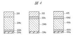
図4は、メモリMOS型トランジスタの容量絶縁膜の構造を示した断面図である。図4の左図は、Si基板側よりSi酸化膜204a、Si窒化膜204b、Si酸窒化膜204cおよびメモリゲート電極205が積層された状態を示し、各絶縁膜の膜厚はそれぞれ4nm、4nmおよび18nmである。
【0110】
Si窒化膜204bはジクロルシランとアンモニアを原料ガスとするLP−CVD法で形成した。本実施の形態で用いたSi窒化膜204bの電子トラップ密度は5e18/cm3であった。
【0111】
また、Si酸窒化膜204cは実施の形態1のSi酸窒化膜104bと同様に形成することができ、本実施の形態では、酸素濃度を調整して電子トラップ密度を2e18/cm3とした。なお、Si酸窒化膜についての好適な膜厚範囲や酸素濃度範囲は、実施の形態1と同様である。
【0112】
従って、本構造の電荷保持膜は電子トラップ密度と膜厚の積が値の大きいSi酸窒化膜204cとなる。消去動作時のバンド構造は、図14に示した構造となり、Si酸窒化膜204cにトラップされた電子に対しては電位障壁膜は存在しない。
【0113】
一方、メモリゲート電極205近傍で発生した正孔に対しては、下層Si酸化膜204aとSi窒化膜204bの界面に存在する電位障壁が大きいため、正孔のトンネル確率は小さくなる。以上の2つの効果により、Gm劣化は大幅に改善される。
【0114】
ここでは、メモリMOS型トランジスタの容量絶縁膜を、Si酸化膜204a、Si窒化膜204bおよびSi酸窒化膜204cの積層構造としたが、Si窒化膜204bの部分をSi酸窒化膜としてもよい。即ち、Si酸化膜204a、Si酸窒化膜(1)204bおよびSi酸窒化膜(2)204cの積層構造としてもよい。但し、図4の左図に示す場合と同様の効果を得るためには、Si酸窒化膜(1)204bの酸素濃度をSi酸窒化膜(2)204cより小さくし、さらに、Si酸窒化膜(1)とSi酸窒化膜(2)の膜厚と電子トラップ密度をそれぞれT1、N1、T2、N2とした場合、「T1<(N2×T2)/N1」の条件を満たす必要がある。
【0115】
図4の中央図は、Si基板側よりSi酸化膜304a、Si酸窒化膜304b、Si窒化膜304cおよびメモリゲート電極305が積層された状態を示し、各絶縁膜の膜厚はそれぞれ4nm、18nmおよび4nmである。
Si酸窒化膜304bおよびSi窒化膜304cの形成方法および電子トラップ密度は、それぞれSi酸窒化膜204cおよびSi窒化膜204bと同様である。
【0116】
従って、本構造の電荷保持膜は電子トラップ密度と膜厚の積が値の大きいSi酸窒化膜304bとなる。消去動作時のバンド構造は、図13の上図に示した構造となり、Si酸窒化膜304bにトラップされた電子に対してSi窒化膜304cは電位障壁膜とならないため低電圧消去が可能となる。一方、メモリゲート電極305近傍で発生した正孔には、Si窒化膜304cとSi酸窒化膜304bの界面が電位障壁になるため、Si基板側に移動する確率が小さくなる。以上の2つの効果によりGm劣化は大幅に改善される。
【0117】
ここでは、メモリMOS型トランジスタの容量絶縁膜を、Si酸化膜304a、Si酸窒化膜304bおよびSi窒化膜304cの積層構造としたが、Si窒化膜304cの部分をSi酸窒化膜としてもよい。即ち、Si酸化膜304a、Si酸窒化膜(1)304bおよびSi酸窒化膜(2)304cの積層構造としてもよい。但し、図4の中央図に示す場合と同様の効果を得るためには、Si酸窒化膜(2)304cの酸素濃度をSi酸窒化膜(1)304bより小さくし、さらに、Si酸窒化膜(1)とSi酸窒化膜(2)の膜厚と電子トラップ密度をそれぞれT1、N1、T2、N2とした場合、「T2<(N1×T1)/N2」の条件を満たす必要がある。
【0118】
図4の右図は、Si基板側よりSi酸化膜404a、Si窒化膜404b、Si酸窒化膜404c、Si窒化膜404dおよびメモリゲート電極405が積層された状態を示し、各絶縁膜の膜厚はそれぞれ4nm、3nm、17nmおよび3nmである。Si酸窒化膜404cおよびSi窒化膜404b、404dの形成方法および電子トラップ密度は、それぞれSi酸窒化膜204cおよびSi窒化膜204bと同様である。
【0119】
従って、本構造の電荷保持膜は電子トラップ密度と膜厚の積が最も大きいSi酸窒化膜404cとなる。消去動作時のバンド構造は、図15に示した構造となり、Si酸窒化膜404cにトラップされた電子に対して上層のSi窒化膜404dは電位障壁膜とならないため低電圧消去が可能となる。一方、メモリゲート電極405近傍で発生した正孔には、Si窒化膜404dとSi酸窒化膜404cとの界面、およびSi窒化膜404dとSi酸化膜404aの界面が電位障壁になるため、Si基板側に移動する確率は非常に小さくなる。以上の2つの効果によりGm劣化は大幅に改善される。
【0120】
ここでは、メモリMOS型トランジスタの容量絶縁膜を、Si酸化膜404a、Si窒化膜404b、Si酸窒化膜404cおよびSi窒化膜404dの積層構造としたが、Si酸窒化膜404cの上下層のSi窒化膜404bおよび404dをSi酸窒化膜としてもよい。即ち、Si酸化膜404a、Si酸窒化膜(1)404b、Si酸窒化膜(2)404cおよびSi酸窒化膜(3)404dの積層構造としてもよい。但し、図4の左図に示す場合と同様の効果を得るためには、Si酸窒化膜(2)304cの酸素濃度をSi酸窒化膜(1)404bおよびSi酸窒化膜(3)404dより大きくし、さらに、Si酸窒化膜(1)、Si酸窒化膜(2)およびSi酸窒化膜(3)の膜厚と電子トラップ密度をそれぞれT1、N1、T2、N2、T3、N3とした場合、「T1<(N2×T2)/N1」および「T3<(N2×T2)/N3」の条件を満たす必要がある。
【0121】
なお、上記膜の積層例の他、図11の欄7に示すように、図4の左図のSi窒化膜204bをSi酸窒化膜とSi窒化膜の積層膜とし(欄7の(b)参照)、また、図4の中央図のSi窒化膜304cをSi酸窒化膜とSi窒化膜の積層膜としてもよい(欄7の(a)参照)。
【0122】
なお、本実施の形態においても、単結晶Si基板上に形成した不揮発性メモリに関して記載したが、本発明は単結晶Si基板に限るものではない。例えば、歪み基板やSOI基板を用いてもよく、また、ガラス基板を用いた薄膜TFT(高温多結晶Si−TFT、低温多結晶Si−TFT)デバイスにも適用できる。
【0123】
(実施の形態3)
実施の形態1においては、電荷蓄積膜としてシリコン酸窒化膜を用いた場合に生じるGmの劣化を上層の電位障壁膜の省略や薄膜化により改善したが、消去方法をホットホール注入とすることによりGm劣化を低減してもよい。
【0124】
即ち、実施の形態1においては、電荷保持膜の電子をメモリゲート電極へ引き抜く消去方式について記述したが、もう1つの低電圧消去法としてホットホール消去が挙げられる。ホットホール消去は、メモリMOS型トランジスタのメモリゲート電極に負バイアス、その拡散層に正バイアスを印加し、バンド間トンネリングを用いてホットホールを電荷保持膜に注入する方式である。ホットホール消去によれば、メモリMOS型トランジスタのメモリゲート電極に正電圧を印加してキャリアを引き抜く方式に比べ、消去電圧を小さく出来る利点がある。このため、Si酸窒化膜を電荷保持膜として用いても、消去時のGm劣化を抑制することが可能となる。
【0125】
次いで、本実施の形態の不揮発性半導体記憶装置の構造およびその駆動方法について詳細に説明する。
【0126】
図5に本実施の形態の不揮発性メモリセルの断面図を示す。実際には図の上層には配線が存在するが本図では省略する。
【0127】
メモリセルはSi基板上に設けたp型ウエル領域501、ソース領域507Bとなるn型拡散層、ドレイン領域507Aとなるn型拡散層を有した2つのMOS型トランジスタから構成されている。選択MOS型トランジスタは、ゲート絶縁膜502となるSi酸化膜、選択ゲート電極503となるn型多結晶Si膜およびその上部に形成した絶縁膜504から構成されている。メモリMOS型トランジスタはp型ウエル領域501との下層電位障壁膜504aとなるSi酸化膜、電荷保持膜504bとなるSi酸窒化膜、メモリゲート電極505との電位障壁膜504cとなるSi酸化膜およびメモリゲート電極505となるn型多結晶Si膜から構成されている。
【0128】
2つのトランジスタのゲート電極503、505は、ギャップ絶縁膜506となるSi酸化膜で電気的に分離されており、このギャップ絶縁膜506はメモリMOS型トランシスタの下層電位障壁膜504aや選択MOS型トランジスタのゲート絶縁膜502とは別層で形成されている。選択MOS型トランジスタのゲート絶縁膜502およびメモリMOS型トランジスタのp型ウエル領域501に対する下層電位障壁膜504aは、例えばp型ウエル領域501を酸化性雰囲気中で熱酸化して形成したSi酸化膜であり、膜厚はそれぞれ3nmおよび7nmである。
【0129】
電荷保持膜504bであるSi酸窒化膜は、実施の形態1のSi酸窒化膜104bと同様に形成することができるが、本実施の形態では、膜中酸素濃度をパラメータとして、0%(Si窒化膜)〜30%の間で変化させて検討した。Si酸窒化膜は膜中の酸素濃度により誘電率が変化するため、全ての試料は物理膜厚を調整することで、Si酸化膜に換算した膜厚で統一した。本実施の形態におけるSi酸窒化膜の膜厚許容範囲は、上限が消去速度、下限は書込み速度で決定される。消去速度の面からは15nm以下、書込み速度の面からは5nm以上、より好ましくは13nm以下、7nm以上である。
【0130】
メモリゲート電極505に対する上層電位障壁膜504cは、Si酸化膜であり、例えばジクロルシランと亜酸化窒素を原料ガスとするLP−CVD法で6nm程度のSi酸化膜を堆積した後、900℃の水蒸気雰囲気中で10分間の熱処理を行うことにより形成する。メモリゲート電極505は、LP−CVD法でn型多結晶Si膜を形成した後、異方性ドライエッチングによりパターン段差の側壁部にだけn型多結晶Si膜を残存させることにより形成する。
【0131】
本実施の形態ではメモリゲート電極505をサイドウォール形状としたが、これは電荷保持膜504bの電子の注入領域とホットホール注入領域の距離を短くして、消去効率を向上させるためである。従って、図1に示した構造のメモリセル等を用いても、ホットホール消去は可能である。
【0132】
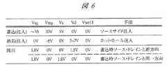
図6に、図5に示したメモリセルの動作と電圧の掛け方の一例を示す。ここでは、電荷保持膜504bへの電荷注入を書込み(program)と定義する。書込み方式は、ソースサイド・インジェクションを用いたホットエレクトロン書込みである。例えば、ソース領域507Bに印加する電圧(Vs)は5V、ドレイン領域507Aに印加する電圧(Vd)は0V、メモリMOS型トランジスタのゲート電極505に印加する電圧(Vmg)は10V、選択MOS型トランジスタのゲート電極103へ印加する電圧(Vsg)は、そのトランジスタのしきい値(Vt)と概ね同じとする。ホットエレクトロンの発生領域は、2つのトランジスタのゲート電極503、505が絶縁された領域下のチャネル部である。書込みはトランジスタのしきい値が5Vになるように設定した。
【0133】
消去は、バンド間トンネリングを用いたホットホール注入消去である。メモリMOS型トランジスタのゲート電極505に印加する電圧は(Vmg)は−6V、ドレイン領域507Aに印加する電圧(Vd)は5〜7V、その他の電圧は0Vとして、トランジスタのしきい値が−1Vになるまで消去を行った。なお、図6に示した電圧条件および書込み/消去のしきい値の絶対値は一例であり、この数値をもって本発明が限定されるわけではない。
【0134】
作製した試料の書込み/消去特性は、電荷保持膜504bの酸素濃度が大きい試料ほど書込み時間は長く、消去時間は短くなったが、いずれの場合も所定の時間内で書込み/消去は終了した。また、酸素濃度が30%を越えると所定の時間内に書込みが出来なかった。従って、書込み速度の観点からは、Si酸窒化膜の酸素濃度は30%以下の範囲で使用すことが望ましい。また、電荷保持特性の観点から酸素濃度は5%以上とすることが望ましい。
【0135】
また、書込み/消去の1000回繰り返しによるGm劣化率を評価した結果、Si酸窒化膜特有のGm劣化率の増加は観測されずSi窒化膜と同等の値を示した。
【0136】
一方、電荷保持特性においては、Si窒化膜に比べSi酸窒化膜の方が良好な特性を示した。また、Si酸窒化膜で比較した場合、酸素濃度が大きい試料ほど良好な電荷保持特性が得られた。電荷保持特性の評価は、書込み直後と高温放置後のしきい値を比較する方法で評価した。具体的にはメモリMOS型トランジスタのゲート電極に1.5Vの電圧を印加し、145℃で10万秒放置した後のしきい値の差で比較した。なお、電荷保持特性の電圧条件、放置温度、放置時間の絶対値は一例であり、この数値をもって本発明が限定されるわけではない。
【0137】
以上詳細に説明したように、前記実施の形態1〜3によれば、電荷保持絶縁膜を用いた分散記憶型不揮発性メモリの電荷保持特性の向上と、書込み/消去の繰り返し動作による相互コンダクタンスの劣化の改善を両立できる。
【0138】
以上、本発明者によってなされた発明を実施の形態に基づき具体的に説明したが、本発明は前記実施の形態に限定されるものではなく、その要旨を逸脱しない範囲で種々変更可能であることはいうまでもない。
【0139】
また、本発明の不揮発性メモリは、マイクロコンピュータに用いるなど、種々の装置に搭載可能である。
【0140】
【発明の効果】
本願によって開示される発明のうち、代表的なものによって得られる効果を簡単に説明すれば、以下の通りである。
【0141】
不揮発性半導体記憶装置の性能の向上を図ることができる。
【0142】
特に、電荷保持特性の向上を図ることができる。また、電流駆動能力の劣化を防止することができる。また、動作速度の向上を図ることができる。
【図面の簡単な説明】
【図1】本発明の実施の形態1である不揮発性メモリの要部断面図である。
【図2】本発明の実施の形態1の不揮発性メモリの電圧印加条件を示す図表である。
【図3】本発明の実施の形態1の効果を示すためのグラフである。
【図4】本発明の実施の形態2である不揮発性メモリの容量絶縁膜部の要部断面図である。
【図5】本発明の実施の形態3である不揮発性メモリの要部断面図である。
【図6】本発明の実施の形態3の不揮発性メモリの電圧印加条件を示す図表である。
【図7】本発明の不揮発性メモリと対比するための不揮発性メモリの要部断面図である。
【図8】本発明の不揮発性メモリと対比するための不揮発性メモリの要部断面図である。
【図9】本発明者らが事前に検討した不揮発性メモリの要部断面図である。
【図10】電荷保持膜中の横方向の電子分布を模式的に示すグラフである。
【図11】実施の形態1〜3に示した不揮発性メモリの容量絶縁膜の構成例を示す図表である。
【図12】正孔発生のモデルを示すバンド構造図である。
【図13】本発明の実施の形態2の不揮発性メモリの容量絶縁膜部の状態を示すバンド構造図である。
【図14】本発明の実施の形態2の不揮発性メモリの容量絶縁膜部の状態を示すバンド構造図である。
【図15】本発明の実施の形態2の不揮発性メモリの容量絶縁膜部の状態を示すバンド構造図である。
【符号の説明】
101 p型ウエル領域(Si基板)
102 ゲート絶縁膜
103 ゲート電極(選択ゲート電極)
104a 下層電位障壁膜(Si酸化膜)
104b Si酸窒化膜(電荷保持膜)
104c 上層電位障壁膜(Si酸化膜)
105 ゲート電極(メモリゲート電極)
106 ギャップ絶縁膜
107A ドレイン領域
107B ソース領域
204a Si酸化膜(下層電位障壁膜)
204b Si窒化膜
204c Si酸窒化膜
205 メモリゲート電極
304a Si酸化膜
304b Si酸窒化膜
304c Si窒化膜
305 メモリゲート電極
404a Si酸化膜
404b Si窒化膜
404c Si酸窒化膜
404d Si窒化膜
405 メモリゲート電極
501 p型ウエル領域(Si基板)
502 ゲート絶縁膜
503 ゲート電極(選択ゲート電極)
504 絶縁膜
504a 下層電位障壁膜
504b 電荷保持膜
504c 上層電位障壁膜
505 ゲート電極(メモリゲート電極)
506 ギャップ絶縁膜
507A ドレイン領域
507B ソース領域
601 Si基板(p型ウエル領域)
602 ゲート絶縁膜
603 ゲート電極(選択ゲート電極)
604 容量絶縁膜
604a Si酸化膜(第1層膜)
604b Si窒化膜(第2層膜)
604c Si酸化膜(第3層膜)
605 ゲート電極(メモリゲート電極)
607A 拡散層(ドレイン領域)
607B 拡散層(ソース領域)
701 Si基板(p型ウエル領域)
702 ゲート絶縁膜
703 ゲート電極(選択ゲート電極)
704 容量絶縁膜
704a 第1層膜
704b Si窒化膜(第2層膜)
704c 第3層膜
705 ゲート電極
706 ギャップ絶縁膜
707A 拡散層(ドレイン領域)
707B 拡散層(ソース領域)
709 絶縁膜
801 Si基板(p型ウエル領域)
802 ゲート絶縁膜
803 選択ゲート電極
804 容量絶縁膜
805 ゲート電極(メモリゲート電極)
806 ギャップ絶縁膜
807A 拡散層(ドレイン領域)
807B 拡散層(ソース領域)
Gm 電流駆動能力[0001]
BACKGROUND OF THE INVENTION
The present invention relates to a nonvolatile semiconductor memory device, and more particularly to a highly reliable nonvolatile semiconductor memory device capable of low voltage and high speed programming.
[0002]
[Prior art]
Typical examples of non-volatile memories (non-volatile semiconductor memory devices) using an insulating film as a storage node include MNOS (Metal-Nitride-Oxide-Semiconductor) memory and MONOS (Metal-Oxide-Nitride-Oxide-Semiconductor) memory. It is done. The MNOS memory has a stacked structure of a conductive gate electrode (M), a silicon nitride film (N, hereinafter referred to as “Si nitride film”), a silicon oxide film (O, hereinafter referred to as “Si oxide film”), and a semiconductor substrate (S). The MONOS memory has a laminated structure of a conductive gate electrode (M), a Si oxide film (O), a Si nitride film (N), a Si oxide film (O), and a semiconductor substrate (S). Both store information by injecting and releasing carriers into a Si nitride film having a charge holding function.
[0003]
Regarding the structure and programming method of the non-volatile memory, for example, Patent Document 1 (Japanese Patent Laid-Open No. 2001-102466 (corresponding USP 6,255,166)), Patent Document 2 (Japanese Patent Laid-Open No. 2001-148434) and Patent This is disclosed in Document 3 (USP 5,969,383) and the like.
[0004]
Hereinafter, the structure and operation of a memory cell of the type disclosed in Patent Document 1 (Japanese Patent Laid-Open No. 2001-102466) and Patent Document 2 (Japanese Patent Laid-Open No. 2001-148434) will be briefly described with reference to FIG. .
[0005]
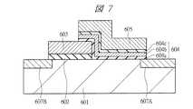
This non-volatile memory is composed of two MOS transistors, a memory MOS transistor that constitutes a storage unit, and a selection MOS transistor for selecting the memory unit and reading information. The diffusion layer (source region) 607B of the selection MOS transistor is connected to the bit line, and the
[0006]
The
[0007]
The Si nitride film as the
[0008]
In the write operation, a predetermined voltage is applied to the diffusion layer (source region) 607B of the selection MOS transistor and its
[0009]
The erase operation is roughly divided into two. One is a method of extracting carriers from the Si
[0010]
In the read operation, when the selection MOS transistor is turned on, the stored information is read depending on whether or not a predetermined current flows depending on the threshold voltage state of the memory MOS transistor.
[0011]
Next, the structure and operation of a memory cell of the type disclosed in Patent Document 3 (US Pat. No. 5,969,383) will be briefly described with reference to FIG.
[0012]
This nonvolatile memory is also composed of two MOS transistors, that is, a memory MOS transistor that constitutes a storage unit and a selection MOS transistor that selects the memory unit and reads information. The diffusion layer (source region) 707B of the selection MOS transistor is connected to the bit line, and the
[0013]
The
[0014]
In the write operation, a predetermined voltage is applied to the diffusion layer (source region) 707B of the selection MOS transistor and its
[0015]
The erasing operation is performed by applying a negative bias to the
[0016]
In the read operation, when the selection MOS transistor is turned on, the stored information is read depending on whether or not a predetermined current flows depending on the threshold voltage state of the memory MOS transistor.
[0017]
[Patent Document 1]
JP 2001-102466 A (corresponding USP 6,255,166)
[0018]
[Patent Document 2]
JP 2001-148434 A
[0019]
[Patent Document 3]
USP 5,969,383
[0020]
[Problems to be solved by the invention]
The inventors of the present invention are engaged in research and development of nonvolatile semiconductor memory devices, and are conducting various studies on performance enhancement of the devices.
[0021]
For example, increase the speed of writing and erasing, suppress the current drive capability Gm degradation accompanying writing and erasing, improve the charge retention characteristics, etc., and the method of high speed writing and erasing Are considering.
[0022]
In particular, as a result of the study by the present inventors, which will be described in detail later, it has been found that using a Si oxynitride film as the charge retention insulating film speeds up writing and erasing and improves the charge retention characteristics.
[0023]
[0024]
Further, as a result of further investigation, it has been found that when the Si oxynitride film is used as the charge retention insulating film, the above characteristics can be improved while the current driving capability Gm is deteriorated. The deterioration of the current driving capability Gm will be described in detail later.
[0025]
An object of the present invention is to improve the performance of a nonvolatile semiconductor memory device.
[0026]
In particular, the purpose is to improve the charge retention characteristics. Another object is to prevent deterioration of current drive capability. Another object is to improve the operation speed.
[0027]
The above and other objects and novel features of the present invention will be apparent from the description of this specification and the accompanying drawings.
[0028]
[Means for Solving the Problems]
Of the inventions disclosed in the present application, the outline of typical ones will be briefly described as follows.
[0029]
The nonvolatile semiconductor memory device of the present invention includes (a) first and second semiconductor regions formed in a semiconductor substrate, and (b) formed on the semiconductor substrate above the first and second semiconductor regions. First and second conductors formed; (c) a first insulating film formed between the first conductor and the semiconductor substrate; and (d) the second conductor and the semiconductor substrate. (E) the second insulating film is composed of a potential barrier film on the semiconductor substrate and a silicon oxynitride film above the second insulating film, and the silicon oxide The second conductor is located on the nitride film.
[0030]
The nonvolatile semiconductor memory device according to the present invention includes (a) first and second semiconductor regions formed in a semiconductor substrate, and (b) an upper portion of the semiconductor substrate between the first and second semiconductor regions. (C) a first insulating film formed between the first conductor and the semiconductor substrate; (d) the second conductor and the second conductor; (E) the second insulating film is composed of a potential barrier film on the semiconductor substrate and a charge holding film on the second insulating film. The holding film includes a silicon oxynitride film, and a third insulating film in which a sum of energy from a vacuum level to a conductor of the film and a band gap of the film is smaller than the silicon oxynitride film, The product of the charge trap density and the film thickness of the silicon oxynitride film is the electric charge of the third insulating film. It is greater than the product of trap density and thickness.
[0031]
The nonvolatile semiconductor memory device according to the present invention includes (a) first and second semiconductor regions formed in a semiconductor substrate, and (b) an upper portion of the semiconductor substrate between the first and second semiconductor regions. (C) a first insulating film formed between the first conductor and the semiconductor substrate; (d) the second conductor and the second conductor; And (e) the second insulating film includes a first potential barrier film on the semiconductor substrate, a silicon oxynitride film on the top, and an upper part thereof. (F) The silicon oxynitride film has a charge holding function, and electrons accumulated in the silicon oxynitride film are injected by injecting holes from the semiconductor substrate side. It will be erased.
[0032]
DETAILED DESCRIPTION OF THE INVENTION
Hereinafter, embodiments of the present invention will be described in detail with reference to the drawings. Note that components having the same function are denoted by the same reference symbols throughout the drawings for describing the embodiments, and the repetitive description thereof is omitted.
[0033]
(Embodiment 1)
Before describing the present embodiment, the matters that the present inventors have examined in advance will be described.
[0034]
First, the present inventors examined the relationship between the write / erase characteristics, the read characteristics, and the charge retention characteristics using the film type of the charge retention film of the memory MOS transistor as a parameter.
[0035]
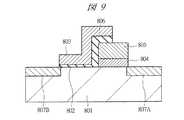
FIG. 9 shows a cross-sectional view of the structure of the memory cell (nonvolatile semiconductor memory device, flash memory) used in this study. The basic element structure is the same as that of the memory cell shown in FIG. 7 except that the
[0036]
Information is written by injecting hot electrons in the channel portion generated by the selection MOS type transistor into the charge holding film which is a part of the
[0037]
Erasing was performed by applying a positive voltage to the
Pulled out to the Morigate electrode.
[0038]
For the charge retention characteristics, (Step 1) writing is performed until a predetermined threshold value is reached, and then (Step 2) a voltage of 1.8 V is applied to the gate electrode of the memory MOS transistor, and the voltage is maintained at 85 ° C. for 100,000 seconds. After leaving, (Step 3) Evaluation was made by comparing the threshold values immediately after writing and after leaving at high temperature.
[0039]
As film types of the charge retention film, an Si nitride film, an Si oxynitride film, a tantalum oxide film, and an aluminum oxide film (alumina film) were examined. Si oxide films were used as potential barrier films above and below the charge retention film. The lower potential barrier film was 4 nm, and the upper potential barrier film was 1.8 nm.
[0040]
In the evaluation of the writing characteristics, when the Si nitride film and the Si oxynitride film were used as the charge holding film, the writing was completed within a predetermined time. On the other hand, when a tantalum oxide film or an alumina film was used, writing could not be performed within a predetermined time. In particular, when a tantalum oxide film was used, even if writing was performed for a long time, the predetermined threshold value was not reached. This is presumably because the tantalum oxide film and the alumina film have a lower electron trap level density than the Si nitride film and the Si oxynitride film. However, when an alumina film is used, the erasing characteristics and the charge holding characteristics are good, so that it is possible to use the alumina film as a charge holding film for a nonvolatile memory that does not require high-speed writing.
[0041]
On the other hand, in the evaluation of erasing characteristics and charge retention characteristics, the use of a Si oxynitride film as the charge retention film increases the erasure speed and superior charge retention characteristics compared to the case of using a Si nitride film. It was newly found to show. Further, the same effect was obtained when the charge retention film was formed as a laminated structure by combining the Si oxynitride film and the Si nitride film. However, this is limited to the case where the thickness of the Si oxynitride film is thicker than that of the Si nitride film, that is, the case where the charge retention amount of the Si oxynitride film is larger than that of the Si nitride film.
[0042]
It can be inferred from the current-voltage characteristics of the Si nitride film and the Si oxynitride film that the erasing speed increases when the Si oxynitride film is used as the charge retention film as follows.
[0043]
That is, it is generally said that the Si nitride film exhibits a PF type conduction mechanism, and the Si oxynitride film exhibits an intermediate conduction mechanism between the PF type and the FN type.
[0044]
Therefore, when comparing the two with an electrically equivalent film thickness (physical film thickness is thin in the Si oxynitride film having a small dielectric constant), the leakage current on the high electric field side is on the Si oxynitride film on the low electric field side. The leakage current is larger in the Si nitride film.
[0045]
In the erasing operation, since a high electric field is applied to the charge holding film, it is considered that the erasing speed is increased in the Si oxynitride film having a large leakage current on the high electric field side.
[0046]
On the contrary, in the charge retention state, the leakage current characteristic on the low electric field side becomes dominant. Therefore, it is considered that the Si oxynitride film having a small leakage current on the low electric field side has improved charge retention characteristics as compared with the Si nitride film.
[0047]
In addition, the charge retention characteristics (threshold voltage fluctuation) are not only the movement of the carriers trapped in the charge retention film in the film thickness direction (movement to the Si substrate side or gate electrode side) but also the lateral diffusion of the film. The effect of.
[0048]
FIG. 10 schematically shows a comparison between the electron distribution immediately after writing and the electron distribution (electron density) after being left at high temperature. The horizontal axis indicates the length from the end of the charge holding film to the horizontal direction of the charge holding film (in the direction of the source region of the memory MOS transistor). (A) shows the electron distribution immediately after writing of the charge holding film, and (b) shows the electron distribution after high temperature holding. (C) shows the electron distribution after holding at a high temperature when a Si nitride film is used.
[0049]
Electrons trapped in the Si nitride film or Si oxynitride film diffuse in the lateral direction within a finite time due to the influence of self-bias and temperature. This electron diffusion is considered to depend on the trap level energy (trap depth) and the density for trapping electrons. When comparing the electron trap level energy, there is no significant difference between the Si nitride film and the Si oxynitride film, but the trap density is smaller in the Si oxynitride film.
[0050]
In addition, the trap density tends to decrease as the oxygen concentration in the Si oxide film increases. For this reason, it is considered that diffusion of electrons injected into the Si oxynitride film is suppressed not only in the film thickness direction but also in the lateral direction of the film.
[0051]
As described above in detail, when the Si oxynitride film is used as the charge holding film, the writing speed is improved, the erasing speed is improved, and the charge holding characteristics are improved as compared with the case where the Si nitride film is used. Improvements in device characteristics were observed.
[0052]
However, as a disadvantage of using a Si oxynitride film, the current drive capability Gm (transconductance as a current supply capability) of the MOS transistor is reduced by repeating the write / erase operation as compared with the case of using a Si nitride film. It became clear to do.
[0053]
As a result of investigating the cause of the decrease in Gm of the element using the Si oxynitride film as the charge retention film, the decrease in Gm is caused by deterioration of the potential barrier film (bottom Si oxide film) below the charge retention film, for example, traps in the film. It was found that the cause was an increase in site and interface state density. Further, it has been found that the deterioration of the bottom Si oxide film is caused by the erasing operation and that holes generated in the charge holding film during the erasing operation are the main causes of the bottom Si oxide film deterioration.
[0054]
Therefore, the present inventors have taken the following measures in order to improve the Gm of the device using the Si oxynitride film.
[0055]
As described above, the decrease in Gm accompanying the write / erase operation of the nonvolatile memory transistor using the Si oxynitride film as the charge retention film is caused by deterioration of the film quality of the bottom Si oxide film (potential barrier film with respect to the Si substrate) accompanying the erase operation. Is the main cause.
[0056]
In order to suppress the degradation of the bottom oxide film due to this erasing operation, (1) lowering the hole generation rate in the charge retention film, (2) lowering the arrival rate of the generated holes to the Si substrate, etc. A method is mentioned.
[0057]
First, a countermeasure for an erasing method in which electrons in the charge retention film are extracted to the gate electrode of the memory MOS transistor will be described. As a means for lowering the hole generation rate in the charge retention film, lowering the erase voltage is the most effective. In order to reduce the erase voltage, it is essential to reduce the thickness of the capacitor insulating film (including the charge retention film) of the memory MOS transistor.
[0058]
However, there are the following restrictions on the thinning of each layer. The lower potential barrier film in contact with the Si substrate needs to be set to a thickness that prevents electrons trapped in the charge holding film from tunneling to the Si substrate side. In terms of the thickness converted to the Si oxide film, about 3 nm is the limit of thinning.
[0059]
The thinning of the charge holding film is not preferable for realizing a high-speed non-volatile memory because it involves an increase in the writing time.
[0060]
Because of the above limitations, the most effective method for realizing a lower erasure voltage is to reduce the thickness of the potential barrier film located above the charge holding film. Specifically, it is desirable that the Si oxide film equivalent film thickness is 1 nm or less. More desirably, the upper potential barrier film is not formed. Strictly speaking, a natural oxide film of about 0.5 nm is formed on the surface of the charge holding film. For example, when the upper potential barrier film and the upper memory gate electrode are formed in different chambers (processing chambers), the semiconductor wafer is exposed to the atmosphere during transportation of the semiconductor wafer, and the surface of the charge retention film is naturally oxidized. A film is formed.
[0061]
Therefore, it is preferable that the upper potential barrier film has a thickness of 1 nm or less, and it is desirable to suppress the upper potential barrier film to 0.5 nm or less, which is the thickness of the natural oxide film. Furthermore, it is desirable not to form an upper potential barrier film. In order to avoid the formation of the natural oxide film as much as possible, there are methods such as avoiding contact between the semiconductor wafer and the atmosphere (oxygen) between the processing steps, and removing the natural oxide film before forming the memory gate electrode. Conceivable. Specifically, if an apparatus having a load lock chamber, a transfer chamber, and a plurality of processing chambers is used, a memory gate electrode can be continuously formed without exposure to the atmosphere after the formation of the charge retention film. The film can be reduced.
[0062]
Next, the structure of the nonvolatile semiconductor memory device of this embodiment and the driving method thereof will be described in detail.
[0063]
FIG. 1 shows a cross-sectional view of a nonvolatile memory cell according to
[0064]
The memory cell includes a p-
[0065]
The selection MOS transistor is composed of a Si oxide film to be a
[0066]
The memory MOS transistor includes a Si oxide film serving as a lower
[0067]
As an example of this embodiment, the capacitor insulating film formed between the
[0068]
The
[0069]
The lower
[0070]
The Si oxynitride film which is the
[0071]
Here, an example of a thermal CVD method using dichlorosilane, ammonia, and nitrous oxide as a source gas is shown as a method for forming a Si oxynitride film, but the present invention is not defined by the type of source gas, and Si As a supply source (Si compound) of hydrogen and silicon compounds such as monosilane and disilane, a halogen and silicon compound such as silicon tetrachloride and silicon hexachloride, and as a supply source of oxygen and nitrogen (oxygen compounds and nitrogen compounds) Of course, it is possible to use hydrazine or nitric oxide. That is, the Si oxynitride film can be formed by chemical vapor deposition using a silicon compound, an oxygen compound and a nitrogen compound or a silicon compound and a compound containing oxygen and nitrogen as raw materials. Further, in the film forming method, other CVD methods such as a plasma CVD method and a catalytic CVD method may be used. Further, the Si oxynitride film may be formed by sputtering (physical vapor deposition method, PVD method). For example, Si is used as a target, and sputtering is performed in an oxidizing and nitriding atmosphere to form a Si oxynitride film.
[0072]
Thus, the Si oxynitride film that is the
[0073]
Further, when the Si oxynitride film is represented by SixOyNz, it is assumed that oxygen (O) in the film is always bonded to two Si and nitrogen (N) is always bonded to three Si (unbonded hands). X, y, z of SixOyNz satisfies 4x = 2y + 3z. However, x + y + z = 1.
[0074]
For example, the nitrogen concentration is preferably 31.4% or more (z ≧ 0.314). The oxygen concentration is preferably 5% or more and 30% or less (0.05 ≦ y ≦ 0.3).
[0075]
Compared with this, for example, the nitrogen concentration of the oxynitride film (the one obtained by nitriding the thermal oxide film) that can be used as the gate insulating film of the select MOS transistor or the lower
[0076]
The upper
[0077]
In the present embodiment, five samples were manufactured by setting the thickness of the
[0078]
In the allowable thickness range of the
[0079]
FIG. 2 shows an example of the operation of the memory cell shown in FIG. 1 and a voltage application method. Here, charge injection into the
[0080]
Erasing was performed by applying a positive voltage to the
[0081]
FIG. 3 shows the relationship between the thickness (nm) of the upper potential barrier film (Si oxide film) 104c, the erase gate voltage (V), and the Gm ratio (%). The Gm ratio is a value obtained by normalizing the Gm after repeating the write / erase operation 1000 times with the initial Gm, and indicates that the Gm ratio is deteriorated as it becomes smaller. As the thickness of the upper
[0082]
In this embodiment, an example of a structure in which the
[0083]
Note that although a nonvolatile memory formed over a single crystal Si substrate is described in this embodiment mode, the present invention is not limited to the single crystal Si substrate. For example, a so-called strained substrate obtained by growing SiGe (silicon germanium) on a Si substrate, or an SOI (silicon on insulator) substrate having single crystal Si can be used. Of course, it is possible to mount a thin film TFT (high temperature polycrystalline Si-TFT, low temperature polycrystalline Si-TFT) and the nonvolatile memory of the present invention on a glass substrate. However, since the low-temperature polycrystalline Si-TFT device has a process temperature limit (for example, 550 ° C. or lower), it is necessary to use a plasma CVD method or a sputtering method to form the capacitive insulating film and the gate electrode. In particular, the formation of the capacitive insulating film is preferably an electron cyclotron resonance (ECR) sputtering method in which a high-quality insulating film is selected even at a low temperature (for example, 550 ° C. or lower).
[0084]
(Embodiment 2)
In the first embodiment, the case where the Si oxynitride film is used as the charge holding film has been described in detail. However, the charge holding film may be a combination of a Si oxynitride film and a Si nitride film. As described above, also in this case, the erasing speed can be increased and the charge retention characteristics can be improved.
[0085]
Here, the “main charge holding film” and “potential barrier film” when the charge holding film is a laminated film are defined as follows. First, the main charge retention film is defined as a film having the largest product of the trap density and the film thickness of injected electrons, that is, a film having the largest amount of trapped electrons. An example in which a plurality of stacked insulating films having a charge holding function are used as charge holding films is shown below. For example, the electron trap density of each of the A film, the B film, and the C film is NA , NB And NC In addition, the film thicknesses of the A film, the B film, and the C film are set to TA , TB , TC "NA × TA <NB × TB <NC × TC The main charge retention film is defined as a C film.
[0086]
The electron trap density of the Si nitride film differs somewhat depending on the formation method. For example, when it is formed by a low pressure chemical vapor deposition method (LP-CVD method) using dichlorosilane and ammonia as source gases, the electron trap density is 4 × 10.18 / CmThree ~ 7 × 10¹⁸ / CmThree (Hereafter, “× 1018 "Is represented as" e18 "). Also, in the Si oxynitride film formed by LP-CVD using dichlorosilane, ammonia, and nitrous oxide as source gases, the electron trap density can be reduced by adjusting the oxygen concentration.2 ) To Si nitride film (SiThree NFour ) Can be controlled within the range. However, if the electron trap density is small, the writing time becomes long, so in reality it is 5e17 / cm.Three It is preferable to use a charge retention film having the above electron trap density.
[0087]
Next, the definition of the potential barrier film will be described. The potential barrier film is defined as a potential barrier film if there is even a slight potential barrier with respect to the gate electrode side when viewed from the electrons trapped in the charge retention film defined by the above formula. Here, the energy (Ea (a)) from the vacuum level to the conduction band (conduction band) of the insulating film A without the electric field applied is the energy (Ea (a)) from the vacuum level to the conduction band of the insulating film B ( If it is smaller than Ea (b)), the insulating film B becomes a potential barrier with respect to the insulating film A. That is, whether or not it becomes a potential barrier is determined by the magnitude of energy from the vacuum level to the conductor of the film.
[0088]
For example, when a bottom Si oxide film, a Si oxynitride film, and a Si nitride film are sequentially stacked from the substrate side, the main charge retention film is a Si oxynitride film as defined by the product of electron trap density and film thickness. Since the upper Si nitride film has a lower carrier barrier than the Si oxynitride film, it does not become a potential barrier film (see FIG. 13 described later). In general, Ea (SiO 2) is about 1 eV and Ea (SiN) is about 2 eV. Therefore, Ea (SiON) is 1 eV to 2 eV (1 eV <Ea (SiON) <2 eV).
[0089]
For example, the energy (electron affinity; κ) from the vacuum level to the conduction band of the Si substrate is 4.1 to 4.15 eV, and the Si substrate and SiO2 The conduction band difference (barrier height; φb1) is about 3.1 eV. Therefore, Ea (SiO2) is the difference between the electron affinity and the barrier height (Si (κ) −φb1 = 4.1 eV−3.1 eV = 1 eV), which is about 1 eV.
[0090]
On the other hand, the difference between the Si substrate and SiN conduction band (barrier height; φb2) is about 2 eV, and Ea (SiN) is (Si (κ) −φb2 = 4.1 eV-2 eV = 2.1 eV), which is about 2.1 eV. Note that the band gap of Si is 1.12 eV.
[0091]
In addition, when the bottom Si oxide film, the Si nitride film, and the Si oxynitride film are sequentially stacked from the substrate side, if the main charge retention film is the uppermost Si oxynitride film, the potential barrier film for the gate electrode side is not exist.
[0092]
FIG. 11 shows an example of the relationship between the main charge holding film and the potential barrier film when a combination of a plurality of insulating films is used as the capacitor insulating film. In the drawing, “
[0093]
For example, the memory cell structure described in the first embodiment corresponds to
[0094]
[0095]
Note that, when a plurality of Si oxynitride films are used as the charge holding film, it is determined whether or not the potential barrier film is formed depending on a difference in oxygen concentration with respect to the charge holding film. As shown in (a) of
[0096]
Thus, when the oxygen concentration of the film is smaller than the oxygen concentration of the Si oxynitride film serving as the charge holding film, it does not become a potential barrier film, but conversely, the oxygen concentration of the film is Si acid serving as the charge holding film. When it is higher than the oxygen concentration of the nitride film, it becomes a potential barrier film. However, as described in the first embodiment, even if a potential barrier film exists between the main charge holding film and the gate electrode, the film thickness is set to 1 nm or less in terms of the Si oxide film equivalent. Gm degradation can be improved.
[0097]
In this way, the amount of holes injected into the Si substrate at the time of erasure is suppressed by forming the Si oxynitride film or the Si oxynitride film having a low oxygen concentration in the upper or lower layer of the Si oxynitride film that becomes the charge retention film be able to. Hereinafter, this point will be described.
[0098]
First, the outline of the mechanism by which holes are generated during erasure will be described with reference to FIG. FIG. 12 is a diagram schematically showing the band structure of the Si substrate, the potential barrier film, the charge holding film, and the gate electrode of the memory MOS transistor at the time of erasing. The generation of holes is considered to reach the Si substrate through the steps 1) to 4) in the figure. The first is the step 1) in which electrons trapped in the trap level of the charge holding film in the vicinity of the memory gate electrode are tunneled to the memory gate electrode, and the second is the charge holding film in the trap level that is vacant. Step 2) in which electrons move from the valence band, 3) Step 3) in which holes generated in the valence band move to the Si substrate side by an electric field, and 4) Valence electrons in the charge retention film This is the step 4) of tunneling the lower potential barrier film from the band. Thus, when holes tunnel through the lower potential barrier film and flow into the Si substrate, an interface state is formed in the Si substrate, and the read current is reduced. As a result, the current driving capability Gm deteriorates.
[0099]
If the upper potential barrier film described in the first embodiment is omitted or made thinner, the erase gate voltage can be lowered, and the probabilities 1), 3) and 4) in the figure are lowered. As a result, generation of holes is suppressed and Gm degradation is also improved.
[0100]
On the other hand, a method in which two or more charge holding films having different band gaps are stacked to form a potential barrier for only holes during the erase operation is also an effective means for improving Gm degradation.
[0101]
FIG. 13, FIG. 14 and FIG. 15 are diagrams schematically showing a band structure when a Si nitride film and a Si oxynitride film are stacked. 13 corresponds to
[0102]
The definition of whether or not it becomes a potential barrier for holes is determined by the magnitude of the sum of the energy from the vacuum level to the conductor of the film and the band gap of the film. With no electric field applied, the sum of the energy (Ea (a)) from the vacuum level to the conduction band (conductive band) of the insulating film A and the band gap (BG (a)) of the insulating film A is the vacuum level. If the energy (Ea (b)) from the position to the conduction band of the insulating film B is smaller than the sum of the band gap (BG (b)) of the insulating film B, the insulating film A becomes a potential barrier for holes. For example, the energy from the vacuum level of SiON to the conduction band (conductive band) shown in FIG. 13 is Ea (SiON), and the band gap is BG (SiON). The numerical value varies slightly depending on the manufacturing method.2 The band gap (BG (SiO 2)) is 8 eV or less, and the band gap (BG (SiN)) of SiN is about 4.4 to 4.6 eV.
[0103]
FIGS. 13 to 15 show examples of the Si nitride film. As shown in the column 5 (a) and the column 7 (a) of FIG. A Si oxynitride film having a low concentration (high nitrogen concentration) may be used.
[0104]
In this way, by combining the charge retention film during the erase operation or an insulating film having a different band gap that serves as a potential barrier against holes generated in the vicinity of the electrodes, positive holes are trapped and reach the Si substrate side. Holes are suppressed. As a result, Gm degradation is also improved.
[0105]
That is, when the main charge retention film is a Si oxynitride film, an Si nitride film, or a Si oxynitride film having a lower oxygen concentration (higher nitrogen concentration) than the main charge retention film, in the upper layer, the lower layer, or in the middle thereof By providing, Gm degradation is improved.
[0106]
Such a film for trapping holes is preferably arranged in the upper layer or the lower layer rather than in the middle of the main charge retention film. This is because when the electrons trapped in the main charge retention film are erased to the gate electrode side, the film becomes a groove (sink) for the electrons, and the erase time increases.
[0107]
Further, according to the study of the present inventor, the Gm deterioration is improved when the hole trapping film is arranged in the lower layer of the charge holding film, and it is preferable to put the film in the lower layer than the upper layer of the charge holding film. . This is because the potential barrier layer on the Si substrate side has the largest potential barrier against trapped holes, and the probability of holes reaching the Si substrate is reduced.
[0108]
Next, the structure of the nonvolatile semiconductor memory device of this embodiment will be described in detail. A memory cell of the same type as in the first embodiment described with reference to FIG. 1 was formed, and the same evaluation as in the first embodiment was performed. This memory cell is a nonvolatile memory having a selection MOS type transistor and a memory MOS type transistor, and is different from the memory cell of the first embodiment (FIG. 1) in the film configuration of the capacitor insulating film of the memory MOS type transistor. is there. Since the materials and forming methods of other parts are the same as those in the first embodiment, description thereof is omitted. Further, since the operation method is the same as that of the first embodiment, the description thereof is omitted.
[0109]
FIG. 4 is a cross-sectional view showing the structure of the capacitor insulating film of the memory MOS transistor. 4 shows a state in which the
[0110]
The
[0111]
Further, the
[0112]
Therefore, the charge retention film of this structure becomes the
[0113]
On the other hand, for the holes generated in the vicinity of the
[0114]
Here, the capacitor insulating film of the memory MOS transistor has a stacked structure of the
[0115]
4 shows a state in which the
The formation method and the electron trap density of the
[0116]
Therefore, the charge retention film of this structure becomes the
[0117]
Here, the capacitor insulating film of the memory MOS transistor has a stacked structure of the
[0118]
4 shows a state in which the
[0119]
Therefore, the charge retention film of this structure becomes the
[0120]
Here, the capacitive insulating film of the memory MOS transistor has a stacked structure of the
[0121]
In addition to the above film stacking example, as shown in
[0122]
Although this embodiment mode also describes the nonvolatile memory formed on the single crystal Si substrate, the present invention is not limited to the single crystal Si substrate. For example, a strained substrate or an SOI substrate may be used, and the present invention can also be applied to a thin film TFT (high temperature polycrystalline Si-TFT, low temperature polycrystalline Si-TFT) device using a glass substrate.
[0123]
(Embodiment 3)
In the first embodiment, the deterioration of Gm that occurs when a silicon oxynitride film is used as the charge storage film is improved by omitting the upper potential barrier film or reducing the thickness, but by using hot hole injection as the erasing method. Gm degradation may be reduced.
[0124]
That is, in the first embodiment, an erasing method in which electrons in the charge holding film are extracted to the memory gate electrode has been described. Another low-voltage erasing method includes hot hole erasing. Hot hole erasing is a system in which a negative bias is applied to the memory gate electrode of the memory MOS transistor and a positive bias is applied to the diffusion layer, and hot holes are injected into the charge holding film using interband tunneling. Hot hole erasing has an advantage that the erasing voltage can be reduced as compared with a method in which a positive voltage is applied to the memory gate electrode of the memory MOS transistor to extract carriers. For this reason, even if the Si oxynitride film is used as the charge holding film, it is possible to suppress the Gm deterioration during erasing.
[0125]
Next, the structure of the nonvolatile semiconductor memory device of this embodiment and the driving method thereof will be described in detail.
[0126]
FIG. 5 shows a cross-sectional view of the nonvolatile memory cell of this embodiment. Actually, wiring exists in the upper layer of the figure, but it is omitted in this figure.
[0127]
The memory cell is composed of two MOS transistors having a p-
[0128]
The
[0129]
The Si oxynitride film as the
[0130]
The upper
[0131]
In this embodiment mode, the
[0132]
FIG. 6 shows an example of the operation and voltage application of the memory cell shown in FIG. Here, charge injection into the
[0133]
Erase is hot hole injection erase using interband tunneling. The voltage applied to the
[0134]
As for the writing / erasing characteristics of the manufactured sample, the writing time was longer and the erasing time was shorter as the sample having a higher oxygen concentration in the
[0135]
Further, as a result of evaluating the Gm deterioration rate after 1000 times of writing / erasing, no increase in the Gm deterioration rate peculiar to the Si oxynitride film was observed, and the same value as that of the Si nitride film was shown.
[0136]
On the other hand, in terms of charge retention characteristics, the Si oxynitride film showed better characteristics than the Si nitride film. Further, when compared with a Si oxynitride film, a sample having a higher oxygen concentration has better charge retention characteristics. The charge retention characteristics were evaluated by a method of comparing threshold values immediately after writing and after being left at high temperature. Specifically, a voltage of 1.5 V was applied to the gate electrode of the memory MOS type transistor, and the comparison was made based on the difference in threshold value after being left at 145 ° C. for 100,000 seconds. Note that the voltage conditions of the charge retention characteristics, the leaving temperature, and the absolute value of the standing time are examples, and the present invention is not limited by these numerical values.
[0137]
As described above in detail, according to the first to third embodiments, the charge retention characteristics of the distributed storage nonvolatile memory using the charge retention insulating film are improved, and the mutual conductance is improved by the repeated write / erase operations. It is possible to improve deterioration.
[0138]
As mentioned above, the invention made by the present inventor has been specifically described based on the embodiment. However, the present invention is not limited to the embodiment, and various modifications can be made without departing from the scope of the invention. Needless to say.
[0139]
Further, the nonvolatile memory of the present invention can be mounted on various devices such as a microcomputer.
[0140]
【The invention's effect】
The effects obtained by the representative ones of the inventions disclosed by the present application will be briefly described as follows.
[0141]
The performance of the nonvolatile semiconductor memory device can be improved.
[0142]
In particular, charge retention characteristics can be improved. Further, it is possible to prevent the current driving capability from being deteriorated. Further, the operation speed can be improved.
[Brief description of the drawings]
FIG. 1 is a cross-sectional view of a main part of a nonvolatile memory according to a first embodiment of the present invention.
FIG. 2 is a table showing voltage application conditions of the nonvolatile memory according to
FIG. 3 is a graph for illustrating the effect of the first embodiment of the present invention.
FIG. 4 is a cross-sectional view of a main part of a capacitor insulating film portion of a nonvolatile memory according to a second embodiment of the present invention.
FIG. 5 is a cross-sectional view of main parts of a nonvolatile memory according to a third embodiment of the present invention.
FIG. 6 is a table showing voltage application conditions of the nonvolatile memory according to the third embodiment of the present invention.
FIG. 7 is a cross-sectional view of a main part of a nonvolatile memory for comparison with the nonvolatile memory of the present invention.
FIG. 8 is a cross-sectional view of a main part of a nonvolatile memory for comparison with the nonvolatile memory of the present invention.
FIG. 9 is a cross-sectional view of a main part of a nonvolatile memory examined in advance by the present inventors.
FIG. 10 is a graph schematically showing the electron distribution in the lateral direction in the charge retention film.
11 is a table showing a configuration example of a capacitor insulating film of the nonvolatile memory shown in
FIG. 12 is a band structure diagram showing a model of hole generation.
FIG. 13 is a band structure diagram showing a state of a capacitor insulating film portion of the nonvolatile memory according to the second embodiment of the present invention;
14 is a band structure diagram showing a state of a capacitor insulating film portion of a nonvolatile memory according to a second embodiment of the present invention; FIG.
FIG. 15 is a band structure diagram showing a state of a capacitor insulating film portion of a nonvolatile memory according to a second embodiment of the present invention;
[Explanation of symbols]
101 p-type well region (Si substrate)
102 Gate insulation film
103 Gate electrode (selection gate electrode)
104a Lower potential barrier film (Si oxide film)
104b Si oxynitride film (charge retention film)
104c Upper potential barrier film (Si oxide film)
105 Gate electrode (memory gate electrode)
106 Gap insulating film
107A drain region
107B source area
204a Si oxide film (lower potential barrier film)
204b Si nitride film
204c Si oxynitride film
205 Memory gate electrode
304a Si oxide film
304b Si oxynitride film
304c Si nitride film
305 Memory gate electrode
404a Si oxide film
404b Si nitride film
404c Si oxynitride film
404d Si nitride film
405 Memory gate electrode
501 p-type well region (Si substrate)
502 Gate insulating film
503 Gate electrode (selection gate electrode)
504 Insulating film
504a Lower potential barrier film
504b Charge holding film
504c Upper potential barrier film
505 Gate electrode (memory gate electrode)
506 Gap insulating film
507A drain region
507B Source area
601 Si substrate (p-type well region)
602 Gate insulating film
603 Gate electrode (selection gate electrode)
604 capacitive insulating film
604a Si oxide film (first layer film)
604b Si nitride film (second layer film)
604c Si oxide film (third layer film)
605 Gate electrode (memory gate electrode)
607A Diffusion layer (drain region)
607B Diffusion layer (source region)
701 Si substrate (p-type well region)
702 Gate insulating film
703 Gate electrode (selection gate electrode)
704 capacitive insulating film
704a First layer film
704b Si nitride film (second layer film)
704c Third layer film
705 Gate electrode
706 Gap insulating film
707A Diffusion layer (drain region)
707B Diffusion layer (source region)
709 Insulating film
801 Si substrate (p-type well region)
802 Gate insulating film
803 Select gate electrode
804 capacitive insulating film
805 Gate electrode (memory gate electrode)
806 Gap insulating film
807A Diffusion layer (drain region)
807B Diffusion layer (source region)
Gm Current drive capability
Claims (14)
Translated fromJapanese(b)前記第1および第2半導体領域の間上に、隣接して配置された第1および第2ゲート電極と、
(c)前記第1ゲート電極と前記半導体基板との間に形成された第1絶縁膜と、
(d)前記第2ゲート電極と前記半導体基板との間に形成された第2絶縁膜と、を有し、
(e)前記第2絶縁膜は、前記半導体基板上に形成された電位障壁膜と、その上部に形成された電荷保持膜よりなり、
前記電荷保持膜に接するように前記電荷保持膜上に前記第2ゲート電極が形成されており、
前記電荷保持膜は、シリコン酸窒化膜と、第3絶縁膜とよりなり、真空準位から前記第3絶縁膜の伝導帯までのエネルギーと、前記第3絶縁膜のバンドギャップとの和が、前記シリコン酸窒化膜より小さく、
前記シリコン酸窒化膜の電荷トラップ密度と膜厚の積は、前記第3絶縁膜の電荷トラップ密度と膜厚の積より大きく、
前記電荷保持膜にトラップした電子を前記第2ゲート電極に引き抜くことにより、消去動作を行なうことを特徴とする不揮発性半導体記憶装置。(A) first and second semiconductor regions formed in a semiconductor substrate;
(B) first and second gate electrodes disposed adjacently between the first and second semiconductor regions;
(C) a first insulating film formed between the first gate electrode and the semiconductor substrate;
(D) having a second insulating film formed between the second gate electrode and the semiconductor substrate;
(E) The second insulating film is composed of a potential barrier film formed on the semiconductor substrate and a charge holding film formed thereon.
The second gate electrode is formed on the charge retention filmso as to be in contact with the charge retention film;
The charge retention film includes a silicon oxynitride film and a third insulating film, and a sum of energy from a vacuum level to a conduction band of the third insulating film and a band gap of the third insulating film is: Smaller than the silicon oxynitride film,
The product of the charge trap density and the film thickness of the silicon oxynitride film is larger than the product of the charge trap density and the film thickness of the third insulating film,
A nonvolatile semiconductor memory device, wherein an erase operation is performed by extracting electrons trapped in the charge retention film to the second gate electrode.
前記シリコン酸窒化膜は、前記第3および第4絶縁膜の間に形成されていることを特徴とする請求項1記載の不揮発性半導体記憶装置。The charge retention film includes a fourth insulating film, and a sum of energy from a vacuum level to a conduction band of the fourth insulating film and a band gap of the fourth insulating film is greater than that of the silicon oxynitride film. small,
2. The nonvolatile semiconductor memory device according to claim 1, wherein the silicon oxynitride film is formed between the third and fourth insulating films.
(b)前記第1および第2半導体領域の間上に、隣接して配置された第1および第2ゲート電極と、
(c)前記第1ゲート電極と前記半導体基板との間に形成された第1絶縁膜と、
(d)前記第2ゲート電極と前記半導体基板との間に形成された第2絶縁膜と、を有し、
(e)前記第2絶縁膜は、前記半導体基板上に形成された電位障壁膜と、その上部に形成された電荷保持膜よりなり、
前記電荷保持膜は、シリコン酸窒化膜と、第3絶縁膜とよりなり、真空準位から前記第3絶縁膜の伝導帯までのエネルギーと、前記第3絶縁膜のバンドギャップとの和が、前記シリコン酸窒化膜より小さく、
前記シリコン酸窒化膜の電荷トラップ密度と膜厚の積は、前記第3絶縁膜の電荷トラップ密度と膜厚の積より大きく、
さらに、前記電荷保持膜に接するように前記電荷保持膜上に形成された第5絶縁膜を有し、
前記第5絶縁膜に接するように前記第5絶縁膜上に前記第2ゲート電極が形成されており、
真空準位から伝導帯までのエネルギーが、前記シリコン酸窒化膜より前記第5絶縁膜の方が小さい場合は、前記第5絶縁膜の膜厚が1nm以下であり、
前記電荷保持膜にトラップした電子を前記第2ゲート電極に引き抜くことにより、消去動作を行なうことを特徴とする不揮発性半導体記憶装置。(A) first and second semiconductor regions formed in the semiconductor substrate;
(B) first and second gate electrodes disposed adjacently between the first and second semiconductor regions;
(C) a first insulating film formed between the first gate electrode and the semiconductor substrate;
(D) having a second insulating film formed between the second gate electrode and the semiconductor substrate;
(E) The second insulating film is composed of a potential barrier film formed on the semiconductor substrate and a charge holding film formed thereon.
The charge retention film includes a silicon oxynitride film and a third insulating film, and a sum of energy from a vacuum level to a conduction band of the third insulating film and a band gap of the third insulating film is: Smaller than the silicon oxynitride film,
The product of the charge trap density and the film thickness of the silicon oxynitride film is larger than the product of the charge trap density and the film thickness of the third insulating film,
And a fifth insulating film formed on the charge retention filmso as to be in contact with the charge retention film,
The second gate electrode is formed on the fifth insulating filmso as to be in contact with the fifth insulating film;
Energy from the vacuum level to the conduction band, when towards said than the silicon oxynitride film fifth insulating film is small,Ri thickness der less 1nm of the fifth insulatingfilm,
The charge by pulling the trapped electrons to the second gate electrode in the holding film,you andperforming an erase operationnonvolatile semiconductor memory device.
Priority Applications (2)
| Application Number | Priority Date | Filing Date | Title |
|---|---|---|---|
| JP2003023690AJP4489359B2 (en) | 2003-01-31 | 2003-01-31 | Nonvolatile semiconductor memory device |
| US10/766,188US6833582B2 (en) | 2003-01-31 | 2004-01-29 | Nonvolatile semiconductor memory device |
Applications Claiming Priority (1)
| Application Number | Priority Date | Filing Date | Title |
|---|---|---|---|
| JP2003023690AJP4489359B2 (en) | 2003-01-31 | 2003-01-31 | Nonvolatile semiconductor memory device |
Publications (3)
| Publication Number | Publication Date |
|---|---|
| JP2004235519A JP2004235519A (en) | 2004-08-19 |
| JP2004235519A5 JP2004235519A5 (en) | 2006-02-23 |
| JP4489359B2true JP4489359B2 (en) | 2010-06-23 |
Family
ID=32952421
Family Applications (1)
| Application Number | Title | Priority Date | Filing Date |
|---|---|---|---|
| JP2003023690AExpired - Fee RelatedJP4489359B2 (en) | 2003-01-31 | 2003-01-31 | Nonvolatile semiconductor memory device |
Country Status (2)
| Country | Link |
|---|---|
| US (1) | US6833582B2 (en) |
| JP (1) | JP4489359B2 (en) |
Families Citing this family (47)
| Publication number | Priority date | Publication date | Assignee | Title |
|---|---|---|---|---|
| JP2006196643A (en)* | 2005-01-13 | 2006-07-27 | Renesas Technology Corp | Nonvolatile semiconductor memory device |
| US7612403B2 (en)* | 2005-05-17 | 2009-11-03 | Micron Technology, Inc. | Low power non-volatile memory and gate stack |
| US7402850B2 (en)* | 2005-06-21 | 2008-07-22 | Micron Technology, Inc. | Back-side trapped non-volatile memory device |
| US7829938B2 (en)* | 2005-07-14 | 2010-11-09 | Micron Technology, Inc. | High density NAND non-volatile memory device |
| TWI260769B (en)* | 2005-08-23 | 2006-08-21 | Ememory Technology Inc | Non-volatile memory and operating method thereof |
| JP2009514194A (en)* | 2005-09-23 | 2009-04-02 | エヌエックスピー ビー ヴィ | Storage element having improved performance and method for manufacturing such storage element |
| US7456465B2 (en) | 2005-09-30 | 2008-11-25 | Freescale Semiconductor, Inc. | Split gate memory cell and method therefor |
| US20070108495A1 (en)* | 2005-11-17 | 2007-05-17 | Macronix International Co., Ltd. | MNOS memory devices and methods for operating an MNOS memory devices |
| WO2007064048A1 (en)* | 2005-12-02 | 2007-06-07 | Nec Corporation | Semiconductor storage device, method for driving same, and method for manufacturing same |
| JP4907999B2 (en)* | 2006-01-20 | 2012-04-04 | 株式会社東芝 | Manufacturing method of semiconductor device |
| US7414889B2 (en)* | 2006-05-23 | 2008-08-19 | Macronix International Co., Ltd. | Structure and method of sub-gate and architectures employing bandgap engineered SONOS devices |
| US7948799B2 (en)* | 2006-05-23 | 2011-05-24 | Macronix International Co., Ltd. | Structure and method of sub-gate NAND memory with bandgap engineered SONOS devices |
| JP5086626B2 (en)* | 2006-12-15 | 2012-11-28 | ルネサスエレクトロニクス株式会社 | Nonvolatile semiconductor memory device and manufacturing method thereof |
| KR101169397B1 (en)* | 2007-01-05 | 2012-07-30 | 삼성전자주식회사 | Semiconductor memory device and manufacturing method of the semiconductor memory device |
| US7416945B1 (en)* | 2007-02-19 | 2008-08-26 | Freescale Semiconductor, Inc. | Method for forming a split gate memory device |
| WO2008123289A1 (en)* | 2007-03-26 | 2008-10-16 | Tokyo Electron Limited | Silicon nitride film and nonvolatile semiconductor memory device |
| JP2008270706A (en)* | 2007-03-26 | 2008-11-06 | Tokyo Electron Ltd | Silicon nitride film and nonvolatile semiconductor memory device |
| US20080237694A1 (en)* | 2007-03-27 | 2008-10-02 | Michael Specht | Integrated circuit, cell, cell arrangement, method for manufacturing an integrated circuit, method for manufacturing a cell, memory module |
| JP2008270343A (en)* | 2007-04-17 | 2008-11-06 | Renesas Technology Corp | Nonvolatile semiconductor memory device |
| US8633537B2 (en) | 2007-05-25 | 2014-01-21 | Cypress Semiconductor Corporation | Memory transistor with multiple charge storing layers and a high work function gate electrode |
| US8614124B2 (en)* | 2007-05-25 | 2013-12-24 | Cypress Semiconductor Corporation | SONOS ONO stack scaling |
| US20090179253A1 (en) | 2007-05-25 | 2009-07-16 | Cypress Semiconductor Corporation | Oxide-nitride-oxide stack having multiple oxynitride layers |
| US8643124B2 (en) | 2007-05-25 | 2014-02-04 | Cypress Semiconductor Corporation | Oxide-nitride-oxide stack having multiple oxynitride layers |
| US9449831B2 (en) | 2007-05-25 | 2016-09-20 | Cypress Semiconductor Corporation | Oxide-nitride-oxide stack having multiple oxynitride layers |
| US9299568B2 (en) | 2007-05-25 | 2016-03-29 | Cypress Semiconductor Corporation | SONOS ONO stack scaling |
| US8940645B2 (en) | 2007-05-25 | 2015-01-27 | Cypress Semiconductor Corporation | Radical oxidation process for fabricating a nonvolatile charge trap memory device |
| US8320191B2 (en) | 2007-08-30 | 2012-11-27 | Infineon Technologies Ag | Memory cell arrangement, method for controlling a memory cell, memory array and electronic device |
| KR100907902B1 (en) | 2007-09-12 | 2009-07-15 | 주식회사 동부하이텍 | Flash memory device and manufacturing method thereof |
| KR20090055202A (en)* | 2007-11-28 | 2009-06-02 | 삼성전자주식회사 | Flash memory devices and cards and systems comprising them |
| US9431549B2 (en) | 2007-12-12 | 2016-08-30 | Cypress Semiconductor Corporation | Nonvolatile charge trap memory device having a high dielectric constant blocking region |
| JP2009224425A (en)* | 2008-03-14 | 2009-10-01 | Renesas Technology Corp | Manufacturing method of nonvolatile semiconductor storage device and nonvolatile semiconductor storage device |
| WO2010082328A1 (en)* | 2009-01-15 | 2010-07-22 | ルネサスエレクトロニクス株式会社 | Semiconductor device, and method for manufacturing the same |
| JP5385307B2 (en)* | 2009-01-15 | 2014-01-08 | ルネサスエレクトロニクス株式会社 | Semiconductor device |
| JP2010183022A (en) | 2009-02-09 | 2010-08-19 | Renesas Electronics Corp | Semiconductor device, and method of manufacturing the same |
| US8198671B2 (en)* | 2009-04-22 | 2012-06-12 | Applied Materials, Inc. | Modification of charge trap silicon nitride with oxygen plasma |
| US8710578B2 (en)* | 2009-04-24 | 2014-04-29 | Cypress Semiconductor Corporation | SONOS stack with split nitride memory layer |
| US9102522B2 (en)* | 2009-04-24 | 2015-08-11 | Cypress Semiconductor Corporation | Method of ONO integration into logic CMOS flow |
| US8222688B1 (en) | 2009-04-24 | 2012-07-17 | Cypress Semiconductor Corporation | SONOS stack with split nitride memory layer |
| KR101546301B1 (en) | 2009-06-22 | 2015-08-21 | 주식회사 동부하이텍 | Non-volatile memory device manufacturing method |
| US8372699B2 (en)* | 2010-02-22 | 2013-02-12 | Freescale Semiconductor, Inc. | Method for forming a split-gate memory cell |
| US8685813B2 (en) | 2012-02-15 | 2014-04-01 | Cypress Semiconductor Corporation | Method of integrating a charge-trapping gate stack into a CMOS flow |
| CN104254921B (en)* | 2012-03-27 | 2020-06-12 | 经度快闪存储解决方案有限责任公司 | SONOS stack with separated nitride storage layer |
| EP2831918A4 (en)* | 2012-03-29 | 2015-11-18 | Cypress Semiconductor Corp | ONO INTEGRATION METHOD IN LOGICAL CMOS FLOW |
| JP6709051B2 (en)* | 2012-03-31 | 2020-06-10 | ロンギチュード フラッシュ メモリー ソリューションズ リミテッド | Oxide-nitride-oxide laminate with multi-layer oxynitride layer |
| US9269822B2 (en)* | 2013-09-12 | 2016-02-23 | Semiconductor Energy Laboratory Co., Ltd. | Semiconductor device and method for manufacturing semiconductor device |
| JP6359432B2 (en)* | 2014-11-27 | 2018-07-18 | ルネサスエレクトロニクス株式会社 | Manufacturing method of semiconductor device |
| US10332599B2 (en)* | 2017-11-14 | 2019-06-25 | Longitude Flash Memory Solutions Ltd. | Bias scheme for word programming in non-volatile memory and inhibit disturb reduction |
Family Cites Families (10)
| Publication number | Priority date | Publication date | Assignee | Title |
|---|---|---|---|---|
| US5969383A (en)* | 1997-06-16 | 1999-10-19 | Motorola, Inc. | Split-gate memory device and method for accessing the same |
| US5879992A (en)* | 1998-07-15 | 1999-03-09 | Taiwan Semiconductor Manufacturing Company, Ltd. | Method of fabricating step poly to improve program speed in split gate flash |
| US6388293B1 (en)* | 1999-10-12 | 2002-05-14 | Halo Lsi Design & Device Technology, Inc. | Nonvolatile memory cell, operating method of the same and nonvolatile memory array |
| US6255166B1 (en)* | 1999-08-05 | 2001-07-03 | Aalo Lsi Design & Device Technology, Inc. | Nonvolatile memory cell, method of programming the same and nonvolatile memory array |
| KR100386611B1 (en)* | 2000-05-08 | 2003-06-02 | 주식회사 하이닉스반도체 | A array of flash memory cell and method for programming of data thereby and method for erased thereby |
| JP4058232B2 (en)* | 2000-11-29 | 2008-03-05 | 株式会社ルネサステクノロジ | Semiconductor device and IC card |
| JP2002261175A (en)* | 2000-12-28 | 2002-09-13 | Sony Corp | Nonvolatile semiconductor memory and its manufacturing method |
| JP4617574B2 (en)* | 2001-01-16 | 2011-01-26 | ソニー株式会社 | Nonvolatile semiconductor memory device and manufacturing method thereof |
| JP4696383B2 (en)* | 2001-03-28 | 2011-06-08 | ソニー株式会社 | Method for manufacturing nonvolatile semiconductor memory device |
| JP2003258128A (en)* | 2002-02-27 | 2003-09-12 | Nec Electronics Corp | Nonvolatile semiconductor memory device, method of manufacturing the same, and method of operating the same |
- 2003
- 2003-01-31JPJP2003023690Apatent/JP4489359B2/ennot_activeExpired - Fee Related
- 2004
- 2004-01-29USUS10/766,188patent/US6833582B2/ennot_activeExpired - Lifetime
Also Published As
| Publication number | Publication date |
|---|---|
| US20040183122A1 (en) | 2004-09-23 |
| US6833582B2 (en) | 2004-12-21 |
| JP2004235519A (en) | 2004-08-19 |
Similar Documents
| Publication | Publication Date | Title |
|---|---|---|
| JP4489359B2 (en) | Nonvolatile semiconductor memory device | |
| US8343840B2 (en) | Blocking dielectric engineered charge trapping memory cell with high speed erase | |
| US7948799B2 (en) | Structure and method of sub-gate NAND memory with bandgap engineered SONOS devices | |
| US7816727B2 (en) | High-κ capped blocking dielectric bandgap engineered SONOS and MONOS | |
| CN101814507B (en) | Depletion Mode Charge Trapping Flash Device | |
| JP5149539B2 (en) | Semiconductor device | |
| US7851827B2 (en) | Back-side trapped non-volatile memory device | |
| JP4907815B2 (en) | Manufacturing method of ONO floating gate electrode in 2-bit EEPROM device | |
| US9361981B2 (en) | Methods of forming and programming memory devices with isolation structures | |
| JP5196500B2 (en) | Storage element and reading method thereof | |
| CN106024889B (en) | Semiconductor device and method for manufacturing the same | |
| JP2011222932A (en) | Nonvolatile memory array having continuous charge storage dielectric stack | |
| CN101494172A (en) | Semiconductor device and method for manufacturing the same | |
| JP4696383B2 (en) | Method for manufacturing nonvolatile semiconductor memory device | |
| JP2002261175A (en) | Nonvolatile semiconductor memory and its manufacturing method | |
| JPS6320387B2 (en) | ||
| CN104425503B (en) | Non-volatile memory semiconductor device and its manufacture method and manufacture device | |
| JP2006196643A (en) | Nonvolatile semiconductor memory device | |
| JP2007103640A (en) | Nonvolatile semiconductor memory device |
Legal Events
| Date | Code | Title | Description |
|---|---|---|---|
| A521 | Request for written amendment filed | Free format text:JAPANESE INTERMEDIATE CODE: A523 Effective date:20060111 | |
| A621 | Written request for application examination | Free format text:JAPANESE INTERMEDIATE CODE: A621 Effective date:20060111 | |
| A977 | Report on retrieval | Free format text:JAPANESE INTERMEDIATE CODE: A971007 Effective date:20090422 | |
| A131 | Notification of reasons for refusal | Free format text:JAPANESE INTERMEDIATE CODE: A131 Effective date:20090908 | |
| A521 | Request for written amendment filed | Free format text:JAPANESE INTERMEDIATE CODE: A523 Effective date:20091105 | |
| A131 | Notification of reasons for refusal | Free format text:JAPANESE INTERMEDIATE CODE: A131 Effective date:20100105 | |
| A521 | Request for written amendment filed | Free format text:JAPANESE INTERMEDIATE CODE: A523 Effective date:20100301 | |
| TRDD | Decision of grant or rejection written | ||
| A01 | Written decision to grant a patent or to grant a registration (utility model) | Free format text:JAPANESE INTERMEDIATE CODE: A01 Effective date:20100323 | |
| A01 | Written decision to grant a patent or to grant a registration (utility model) | Free format text:JAPANESE INTERMEDIATE CODE: A01 | |
| A61 | First payment of annual fees (during grant procedure) | Free format text:JAPANESE INTERMEDIATE CODE: A61 Effective date:20100331 | |
| FPAY | Renewal fee payment (event date is renewal date of database) | Free format text:PAYMENT UNTIL: 20130409 Year of fee payment:3 | |
| R150 | Certificate of patent or registration of utility model | Ref document number:4489359 Country of ref document:JP Free format text:JAPANESE INTERMEDIATE CODE: R150 Free format text:JAPANESE INTERMEDIATE CODE: R150 | |
| A711 | Notification of change in applicant | Free format text:JAPANESE INTERMEDIATE CODE: A712 Effective date:20100528 | |
| A072 | Dismissal of procedure [no reply to invitation to correct request for examination] | Free format text:JAPANESE INTERMEDIATE CODE: A072 Effective date:20100921 | |
| S111 | Request for change of ownership or part of ownership | Free format text:JAPANESE INTERMEDIATE CODE: R313111 | |
| FPAY | Renewal fee payment (event date is renewal date of database) | Free format text:PAYMENT UNTIL: 20130409 Year of fee payment:3 | |
| R350 | Written notification of registration of transfer | Free format text:JAPANESE INTERMEDIATE CODE: R350 | |
| FPAY | Renewal fee payment (event date is renewal date of database) | Free format text:PAYMENT UNTIL: 20140409 Year of fee payment:4 | |
| R250 | Receipt of annual fees | Free format text:JAPANESE INTERMEDIATE CODE: R250 | |
| S531 | Written request for registration of change of domicile | Free format text:JAPANESE INTERMEDIATE CODE: R313531 | |
| R350 | Written notification of registration of transfer | Free format text:JAPANESE INTERMEDIATE CODE: R350 | |
| LAPS | Cancellation because of no payment of annual fees |