JP4489338B2 - Imaging apparatus and control method thereof - Google Patents
Imaging apparatus and control method thereofDownload PDFInfo
- Publication number
- JP4489338B2 JP4489338B2JP2002058135AJP2002058135AJP4489338B2JP 4489338 B2JP4489338 B2JP 4489338B2JP 2002058135 AJP2002058135 AJP 2002058135AJP 2002058135 AJP2002058135 AJP 2002058135AJP 4489338 B2JP4489338 B2JP 4489338B2
- Authority
- JP
- Japan
- Prior art keywords
- image data
- image
- line memory
- clock pulse
- output
- Prior art date
- Legal status (The legal status is an assumption and is not a legal conclusion. Google has not performed a legal analysis and makes no representation as to the accuracy of the status listed.)
- Expired - Fee Related
Links
Images


Classifications
- H—ELECTRICITY
- H04—ELECTRIC COMMUNICATION TECHNIQUE
- H04N—PICTORIAL COMMUNICATION, e.g. TELEVISION
- H04N25/00—Circuitry of solid-state image sensors [SSIS]; Control thereof
- H04N25/60—Noise processing, e.g. detecting, correcting, reducing or removing noise
- H04N25/616—Noise processing, e.g. detecting, correcting, reducing or removing noise involving a correlated sampling function, e.g. correlated double sampling [CDS] or triple sampling
Landscapes
- Engineering & Computer Science (AREA)
- Multimedia (AREA)
- Signal Processing (AREA)
- Transforming Light Signals Into Electric Signals (AREA)
Description
Translated fromJapanese【0001】
【技術分野】
この発明は,撮像装置およびその制御方法に関する。
【0002】
【発明の背景】
ディジタル・スチル・カメラのような撮像装置においては,CCDを用いて被写体が撮像される。被写体像を表す信号がCCDから出力する。CCDの出力信号は,相関二重サンプリング回路により,基準となる黒信号部分(フィードスルー・レベル)と映像信号部分(画素信号部分)とが画素ごとにサンプリングされる。映像信号部分のサンプリング値がディジタル画像データに変換される。
【0003】
ディジタル・スチル・カメラには,2つのライン・メモリが設けられており,1水平走査ライン分の画像データが2つのライン・メモリに交互に書き込まれ,そして読み出される。すなわち,一方のライン・メモリに画像データを書き込んでいるときには,他方のライン・メモリから画像データが読み出される。
【0004】
DMA(Direct Memory Access)コントローラからDMAクロック・パルスが出力され,ライン・メモリに与えられることにより,ライン・メモリに記憶されている画像データが読み出される。
【0005】
CCDの出力信号は,非常に微少であるので,DMAクロック・パルスがCCDの出力信号にノイズとなって現れることがある。ノイズが重畳された映像信号部分をサンプリングすることとなり,表示される被写体像にノイズが現れてしまう。
【0006】
【発明の開示】
この発明は,ノイズが除去されている被写体像を表示できるようにすることを目的とする。
【0007】
第1の発明による撮像装置(ディジタル・スチル・カメラ,ディジタル・ムービ・カメラ,携帯型電子機器にカメラの機能を持たせたものを含む)は,被写体を撮像し,被写体像を表す画像データを出力する固体電子撮像素子,上記固体電子撮像素子の有効撮像領域から得られる1水平走査ライン分の画像データを記憶するライン・メモリ,有効画像表示期間内に,上記固体電子撮像素子から画像データを出力し,かつ上記有効撮像領域から得られる1水平走査ライン分の画像データを記憶するように上記ライン・メモリを制御する制御手段,1水平走査ライン分の画像データを無効画像期間内に読み出すように上記ライン・メモリを制御する読み出し制御手段,および上記読み出し制御手段による読み出し制御のもとに上記ライン・メモリから読み出された画像データによって表される1水平走査ライン分の画像を表示するように表示装置を制御する表示制御手段を備えていることを特徴とする。
【0008】
第1の発明は,上記撮像装置に適した制御方法も提供している。すなわち,この方法は,固体電子撮像素子を用いて被写体を撮像し,被写体像を表す画像データを得,有効画像表示期間内に,上記固体電子撮像素子から画像データを得,かつ上記有効撮像領域から得られる1水平走査ライン分の画像データをライン・メモリに書き込み,無効画像期間内に,1水平走査ライン分の画像データを上記ライン・メモリから読み出し,上記ライン・メモリから読み出された画像データによって表される1水平走査ライン分の画像を表示するように表示装置を制御するものである。
【0009】
第1の発明によると,撮像装置には,上記固体電子撮像素子の有効撮像領域から得られる1水平走査ライン分の画像データを記憶するライン・メモリが設けられている。有効画像表示期間内に,上記固体電子撮像素子から画像データを出力し,かつこの有効画像表示期間内に,有効撮像領域から得られる1水平走査ライン分の画像データが上記ライン・メモリに記憶される。
【0010】
上記ライン・メモリに記憶された1水平走査ライン分の画像データは,無効画像期間内に読み出される。読み出された画像データが表示装置に与えられることにより,撮像により得られた被写体像が表示される。
【0011】
第1の発明によると,有効画像表示期間内に上記固体電子撮像素子から出力された画像データが被写体像の表示のために用いられる。有効画像表示期間内にはライン・メモリからデータの読み出しが行われずに,無効画像期間内に行われる。被写体像の表示に用いられる画像データにはライン・メモリからの画像データの読み出し時に発生するノイズが重畳されないので,被写体像にライン・メモリからの画像データの読み出しにもとづくノイズが表示されることを未然に防止できる。
【0012】
第2の発明による撮像装置は,被写体を撮像し,被写体像を表す信号を出力する固体電子撮像素子,上記固体電子撮像素子の出力信号のうち,映像信号部分を画素ごとにサンプリングするサンプリング回路,上記サンプリング回路によりサンプリングされた映像信号部分をディジタル画像データに変換するアナログ/ディジタル変換回路,上記アナログ/ディジタル変換回路により変換されたディジタル画像データを記憶し,記憶したディジタル画像データを,与えられる読み出しクロック・パルスに応じて画素ごとに読み出す画像メモリ,上記サンプリング回路における映像信号部分のサンプリング後に上記画像メモリに与えるように,上記読み出しクロック・パルスを制御する読み出しクロック・パルス制御手段,および上記画像メモリから出力された画像データによって表される画像を表示するように表示装置を制御する表示制御手段を備えていることを特徴とする。
【0013】
第2の発明は,上記撮像装置に適した制御方法も提供している。すなわち,この方法は,固体電子撮像素子を用いて被写体を撮像し,被写体像を表す信号を得,上記固体電子撮像素子の出力信号のうち,映像信号部分を画素ごとにサンプリングし,サンプリングされた映像信号部分をディジタル画像データに変換し,変換されたディジタル画像データを画像メモリに記憶し,映像信号部分のサンプリング後に上記読み出しクロック・パルスを上記画像メモリに与えて,上記画像メモリに記憶されたディジタル画像データを,画素ごとに読み出し,上記画像メモリから出力された画像データによって表される画像を表示するように表示装置を制御するものである。
【0014】
第2の発明によると,上記固体電子撮像素子の出力信号の映像信号部分が画素ごとにサンプリングされる。サンプリングされた映像信号部分がディジタル画像データに変換され,画像メモリに記憶される。読み出しクロック・パルスが画像メモリに与えられることにより,画像メモリに記憶されている画像データが読み出される。読み出された画像データが表示装置に与えられることにより,撮像により得られた被写体像が表示画面に表示される。
【0015】
画像メモリに与えられる読み出しクロック・パルスは,映像信号のサンプリング後に画素ごとに与えられる。映像信号のサンプリング後に,読み出しクロック・パルスが画像メモリに与えられるので,サンプリングする時点ではノイズが発生していない。ノイズが重畳されていない映像信号部分をサンプリングすることができる。被写体像に画像メモリからの画像データの読み出しにもとづくノイズが重畳することを未然に防止できる。
【0016】
【実施例の説明】
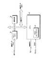
図1は,この発明の実施例を示すもので,ディジタル・スチル・カメラの電気的構成の一部を示すブロック図である。
【0017】
発振回路(図示略)によりマスタ・クロック・パルスMCLKが生成され,PLL(Phase Locked Loop )回路1に入力する。PLL回路1において,位相が確立したマスタ・クロック・パルスMCLKが得られる。PLL回路1から出力されたマスタ・クロック・パルスMCLKは,タイミング・ジェネレータ2および位相制御回路3に入力する。タイミング・ジェネレータ2において,各種パルス等が生成される。
【0018】
タイミング・ジェネレータ2において生成された各種パルス等は,位相制御回路3に入力する。相関二重サンプリング回路9におけるサンプリングのための第1のサンプリング・パルスSH1および第2のサンプリング・パルスSH2,ADクロック・パルスADCLK ならびにCCD6における信号電荷の水平転送のためのパルス等のための信号が位相制御回路3から出力され,相関二重サンプリング回路9,アナログ/ディジタル・コンバータ11およびHドライバ4にそれぞれ与えられる。
【0019】
CCD6は,インターライン型のもので,フォトダイオードに蓄積された信号電荷を垂直方向に転送する垂直転送路および信号電荷を水平方向に転送する水平転送路を備えている。
【0020】
Hドライバ4において,信号電荷を水平方向に転送するための水平転送パルスφHが生成され,CCD6に与えられる。また,Hドライバ4においてリセット・パルスRPも生成され,CCD6に与えられる。さらに,CCD6には,タイミング・ジェネレータ2から水平転送路用のオーバ・フロー・ドレイン・パルスOFDP1が与えられる。
【0021】
Vドライバ5において,信号電荷を垂直方向に転送するための垂直転送パルスφV,フォトダイオードに蓄積された信号電荷を垂直転送路にシフトするためのフィールド・シフト・パルスFSおよび垂直転送路用のオーバ・フロー・ドレイン・パルスOFDP2が生成され,CCD6に与えられる。
【0022】
図2は,CCD6の受光面を示している。
【0023】
CCD6は,水平方向1280画素垂直方向960画素のものであり,約130万個のフォトダイオード(図示略)が配列されている。
【0024】
受光面上における周囲には領域(無効画素領域ということにする。ハッチングで示す。)32がある。この無効画素領域32内のフォトダイオードに蓄積された信号電荷は画像の表示には用いられない。無効画素領域32は,受光面の左側は数十画素分程度,受光面の右側は 100画素程度である。無効画素領域32の内部に領域(有効画素領域ということにする)31がある。有効画素領域31内のフォトダイオードに蓄積された信号電荷が表示装置の表示画面上に表示される画像の生成に用いられることとなる。したがって,無効画素領域32内のフォトダイオードに蓄積された信号電荷によって表される像は表示装置の表示画面上には現れない。
【0025】
図1に戻って,CCD6から出力された信号電荷は,コンデンサ7において蓄積され,映像信号(CCD出力信号という)に変換される。CCD出力信号は,増幅回路8を介して相関二重サンプリング回路9に入力する。
【0026】
上述したように,第1のサンプリング・パルスSH1および第2のサンプリング・パルスSH2にしたがって,相関二重サンプリング回路9において相関二重サンプリングが行われる。相関二重サンプリングについて詳しくは後述する。
【0027】
相関二重サンプリング回路9から出力された映像信号は,増幅回路10において増幅され,アナログ・ディジタル・コンバータ11に入力する。アナログ・ディジタル・コンバータ11において,入力した映像信号がディジタル画像データに変換される。変換されたディジタル画像データがディジタル信号処理回路20に入力する。
【0028】
図3は,ディジタル信号処理回路20の電気的構成を示すブロック図である。
【0029】
ディジタル信号処理回路20には,DMAコントローラ22をもつCPU21が含まれている。CPU21から制御信号が出力され,タイミング・ジェネレータ2に与えられる。
【0030】
アナログ・ディジタル・コンバータ11から出力された画像データは,ライン・メモリ23に与えられる。ライン・メモリ23は,CCD6の有効画素領域31の1水平走査ライン分の画像データを蓄積する容量をもつものである。ライン・メモリ23に書き込まれた1水平走査ライン分の画像データは,DMAコントローラ23の転送クロック・パルスにしたがって読み出され,信号処理回路24に入力する。信号処理回路24において,白バランス調整などの所定の信号処理が行われる。タイミング・ジェネレータ2から垂直同期信号VDおよび水平同期信号HDが与えられ,信号処理回路24において画像データに付加される。信号処理回路24から出力された画像データが外部バスを通してディジタル信号処理回路20から出力される。
【0031】
ディジタル信号処理回路20から出力された画像データが表示装置に与えられることにより,撮像により得られた被写体像が表示画面上に表示される。また,画像データはメモリ・カード(図示略)に与えられ,記録される。
【0032】
図4(A)は,ディジタル・スチル・カメラの各種信号等を示すタイム・チャート,(B)は,表示装置の表示画面を示すものである。
【0033】
上述したように,表示装置の表示画面40はCCD6の有効画素領域31に対応するもので,有効画素領域31内のフォトダイオードに蓄積された信号電荷にもとづいて得られる画像データによって表される画像が表示画面40に表示される。CCD6の無効画素領域32にフォトダイオードに蓄積された信号電荷にもとづいて得られるデータによって表される像は,表示画面40には現れない。
【0034】
この実施例においては,1水平走査期間のうち,有効画素領域31に蓄積された信号電荷をCCD6から読み出す期間(上述したCCD出力信号が得られる期間)を有効画像表示期間といい,無効画素領域32に蓄積された信号電荷をCCD6から読み出す期間を無効画像期間ということにする。
【0035】
上述したライン・メモリ23への1水平走査ライン分の画像データ(有効画素領域31の1水平走査ライン分の画像データ)の書き込みは,有効画像表示期間(たとえば,時刻t11から時刻t12の間)において行われる。ライン・メモリ23からの1水平走査ライン分の画像データの読み出しは,無効画像期間(たとえば,時刻t12から時刻t15の間)の間(たとえば,時刻t13から時刻t14の間)にDMA転送クロック・パルスにしたがって行われる。
【0036】
CCD6からの信号電荷の読み出しからライン・メモリ23への画像データの書き込みまでの処理は,有効画像表示期間内において行われ,ライン・メモリ23からの画像データの読み出しは,無効画像期間内において行われるので,画像データの読み出しにより生じるノイズがCCD出力信号に重畳されてしまうことを未然に防止できる。表示画面40上に表示される画像には,ライン・メモリ23からの画像データの読み出しにもとづいて生じるノイズが重畳することを未然に防止することができる。
【0037】
図5は,他の実施例を示すもので,ディジタル・スチル・カメラの各種信号等を示すタイム・チャートである。
【0038】
上述したマスタ・クロック・パルスMCLKの周期Δt1とDMA転送クロック・パルス(読み出しクロック・パルス)の周期Δt2とは同じであり,位相関係は一定である。マスタ・クロック・パルスMCLKの周期Δt1に対応して1画素分のCCD出力信号が得られる。
【0039】
CCD出力信号のうち,フィード・スルー・レベルの信号が第1のサンプリング・パルスSH1によって相関二重サンプリング回路9においてサンプリングされ(たとえば,時刻t21),画素信号(映像信号,CCD6のフォトダイオードに蓄積された信号電荷の量に対応する)が第2のサンプリング・パルスSH2によって相関二重サンプリング回路9においてサンプリングされる(たとえば,時刻t22)。
【0040】
この実施例においては,第2のサンプリング・パルスSH2の出力後に立ち上がるようにDMA転送クロック・パルスの位相が制御されている。DMA転送クロック・パルスが立ち上がる(たとえば,時刻t22)ことによりノイズNが発生し,CCD出力信号に重畳することがある。第2のサンプリング・パルスSH2の出力後にDMA転送クロック・パルスが立ち上がるので,ノイズNが発生するときにはすでにサンプリングが終わっている。ノイズNの影響を無視することができる。したがって,表示画面に表示される画像はノイズNが除去されたものとなる。
【図面の簡単な説明】
【図1】ディジタル・スチル・カメラの電気的構成の一部を示すブロック図である。
【図2】CCDの受光面を示している。
【図3】ディジタル信号処理回路の電気的構成を示すブロック図である。
【図4】(A)は,ディジタル・スチル・カメラに流れる各種信号のタイム・チャート,(B)は,表示画面を示している。
【図5】他の実施例を示すもので,ディジタル・スチル・カメラに流れる各種信号のタイム・チャートである。
【符号の説明】
2 タイミング・ジェネレータ
3 位相制御回路
6 CCD
9 相関二重サンプリング回路
20 ディジタル信号処理回路
21 CPU
22 DMAコントローラ
23 ライン・メモリ
31 有効撮像領域
32 無効領域
40 表示画面[0001]
【Technical field】
The present invention relates to an imaging apparatus and a control method thereof.
[0002]
BACKGROUND OF THE INVENTION
In an imaging apparatus such as a digital still camera, a subject is imaged using a CCD. A signal representing the subject image is output from the CCD. The output signal of the CCD is sampled for each pixel by a correlated double sampling circuit for a black signal portion (feedthrough level) and a video signal portion (pixel signal portion) as a reference. The sampling value of the video signal portion is converted into digital image data.
[0003]
The digital still camera is provided with two line memories, and image data for one horizontal scanning line is alternately written into and read out from the two line memories. That is, when image data is being written to one line memory, the image data is read from the other line memory.
[0004]
A DMA clock pulse is output from a DMA (Direct Memory Access) controller and applied to the line memory, whereby image data stored in the line memory is read out.
[0005]
Since the output signal of the CCD is very small, the DMA clock pulse may appear as noise in the output signal of the CCD. The video signal portion on which the noise is superimposed is sampled, and noise appears in the displayed subject image.
[0006]
DISCLOSURE OF THE INVENTION
It is an object of the present invention to display a subject image from which noise has been removed.
[0007]
The image pickup apparatus according to the first invention (including a digital still camera, a digital movie camera, and a portable electronic device having a camera function) picks up an image of a subject and outputs image data representing the image of the subject. A solid-state electronic image sensor to output, a line memory for storing image data for one horizontal scanning line obtained from an effective image pickup area of the solid-state electronic image sensor, and image data from the solid-state electronic image sensor within an effective image display period A control means for controlling the line memory so as to output and store image data for one horizontal scanning line obtained from the effective imaging area, and to read out the image data for one horizontal scanning line within the invalid image period Read control means for controlling the line memory, and the line memory under the read control by the read control means Characterized in that it comprises a display control means for controlling the display device to display an image of one horizontal scanning line represented by al read image data.
[0008]
The first invention also provides a control method suitable for the imaging apparatus. That is, in this method, a subject is imaged using a solid-state electronic imaging device, image data representing the subject image is obtained, image data is obtained from the solid-state electronic imaging device within an effective image display period, and the effective imaging area is obtained. The image data for one horizontal scanning line obtained from the above is written to the line memory, and the image data for one horizontal scanning line is read from the line memory within the invalid image period, and the image read from the line memory is read. The display device is controlled to display an image for one horizontal scanning line represented by the data.
[0009]
According to the first invention, the imaging apparatus is provided with a line memory for storing image data for one horizontal scanning line obtained from the effective imaging area of the solid-state electronic imaging device. Image data is output from the solid-state electronic imaging device within the effective image display period, and image data for one horizontal scanning line obtained from the effective imaging area is stored in the line memory within the effective image display period. The
[0010]
The image data for one horizontal scanning line stored in the line memory is read out during the invalid image period. When the read image data is given to the display device, a subject image obtained by imaging is displayed.
[0011]
According to the first invention, the image data output from the solid-state electronic image sensor within the effective image display period is used for displaying the subject image. Data is not read from the line memory within the valid image display period, but is performed within the invalid image period. Since noise generated when reading out image data from the line memory is not superimposed on the image data used to display the subject image, noise based on reading out the image data from the line memory is displayed on the subject image. It can be prevented beforehand.
[0012]
An image pickup apparatus according to a second aspect of the invention is a solid-state electronic image pickup device that picks up an image of a subject and outputs a signal representing the image of the subject. An analog / digital conversion circuit that converts the video signal portion sampled by the sampling circuit into digital image data, stores the digital image data converted by the analog / digital conversion circuit, and reads the stored digital image data as given An image memory that reads out each pixel in response to a clock pulse, a readout clock pulse control means that controls the readout clock pulse so as to give to the image memory after sampling a video signal portion in the sampling circuit, and the image memory Characterized in that it comprises a display control means for controlling the display device to display an image represented by et output image data.
[0013]
The second invention also provides a control method suitable for the imaging apparatus. That is, in this method, a subject is imaged using a solid-state electronic image sensor, a signal representing the subject image is obtained, and a video signal portion of the output signal of the solid-state electronic image sensor is sampled for each pixel and sampled. The video signal portion is converted into digital image data, the converted digital image data is stored in the image memory, and after the video signal portion is sampled, the read clock pulse is applied to the image memory and stored in the image memory. The digital image data is read for each pixel, and the display device is controlled to display an image represented by the image data output from the image memory.
[0014]
According to the second invention, the video signal portion of the output signal of the solid-state electronic image sensor is sampled for each pixel. The sampled video signal portion is converted into digital image data and stored in the image memory. By applying a read clock pulse to the image memory, the image data stored in the image memory is read. When the read image data is given to the display device, a subject image obtained by imaging is displayed on the display screen.
[0015]
The readout clock pulse applied to the image memory is applied to each pixel after sampling the video signal. Since the read clock pulse is applied to the image memory after sampling the video signal, no noise is generated at the time of sampling. It is possible to sample a video signal portion on which noise is not superimposed. It is possible to prevent noise based on reading of image data from the image memory from being superimposed on the subject image.
[0016]
[Explanation of Examples]
FIG. 1 shows an embodiment of the present invention and is a block diagram showing a part of the electrical configuration of a digital still camera.
[0017]
A master clock pulse MCLK is generated by an oscillation circuit (not shown) and input to a PLL (Phase Locked Loop) circuit 1. In the PLL circuit 1, a master clock pulse MCLK whose phase has been established is obtained. The master clock pulse MCLK output from the PLL circuit 1 is input to the timing generator 2 and the phase control circuit 3. In the timing generator 2, various pulses and the like are generated.
[0018]
Various pulses generated by the timing generator 2 are input to the phase control circuit 3. Signals for the first sampling pulse SH1 and the second sampling pulse SH2, AD clock pulse ADCLK for sampling in the correlated double sampling circuit 9 and pulses for horizontal transfer of signal charges in the CCD 6 are provided. It is output from the phase control circuit 3 and supplied to the correlated double sampling circuit 9, the analog / digital converter 11 and the H driver 4, respectively.
[0019]
The CCD 6 is of an interline type and includes a vertical transfer path that transfers signal charges accumulated in the photodiode in the vertical direction and a horizontal transfer path that transfers signal charges in the horizontal direction.
[0020]
In the H driver 4, a horizontal transfer pulse φH for transferring the signal charge in the horizontal direction is generated and applied to the CCD 6. A reset pulse RP is also generated in the H driver 4 and applied to the CCD 6. Further, an overflow drain pulse OFDP1 for the horizontal transfer path is supplied from the timing generator 2 to the CCD 6.
[0021]
In the V driver 5, a vertical transfer pulse φV for transferring the signal charge in the vertical direction, a field shift pulse FS for shifting the signal charge accumulated in the photodiode to the vertical transfer path, and an overload for the vertical transfer path A flow drain pulse OFDP2 is generated and applied to the CCD 6.
[0022]
FIG. 2 shows the light receiving surface of the CCD 6.
[0023]
The CCD 6 has 1280 pixels in the horizontal direction and 960 pixels in the vertical direction, and about 1.3 million photodiodes (not shown) are arranged.
[0024]
There is a region 32 (referred to as an invalid pixel region, indicated by hatching) 32 around the light receiving surface. The signal charges accumulated in the photodiodes in the
[0025]
Returning to FIG. 1, the signal charge output from the CCD 6 is accumulated in the capacitor 7 and converted into a video signal (referred to as a CCD output signal). The CCD output signal is input to the correlated double sampling circuit 9 via the amplifier circuit 8.
[0026]
As described above, correlated double sampling is performed in the correlated double sampling circuit 9 in accordance with the first sampling pulse SH1 and the second sampling pulse SH2. Details of the correlated double sampling will be described later.
[0027]
The video signal output from the correlated double sampling circuit 9 is amplified by the
[0028]
FIG. 3 is a block diagram showing an electrical configuration of the digital
[0029]
The digital
[0030]
The image data output from the analog / digital converter 11 is applied to the line memory 23. The line memory 23 has a capacity for storing image data for one horizontal scanning line in the
[0031]
By applying the image data output from the digital
[0032]
4A is a time chart showing various signals of the digital still camera, and FIG. 4B shows a display screen of the display device.
[0033]
As described above, the
[0034]
In this embodiment, a period during which the signal charge accumulated in the
[0035]
The writing of image data for one horizontal scanning line (image data for one horizontal scanning line in the effective pixel region 31) to the line memory 23 described above is performed in an effective image display period (for example, between time t11 and time t12). Done in The image data for one horizontal scanning line is read from the line memory 23 during the invalid image period (for example, between time t12 and time t15) (for example, between time t13 and time t14). This is done according to the pulse.
[0036]
Processing from reading of signal charges from the CCD 6 to writing of image data to the line memory 23 is performed within the effective image display period, and reading of the image data from the line memory 23 is performed within the invalid image period. Therefore, it is possible to prevent noise generated by reading image data from being superimposed on the CCD output signal. It is possible to prevent the image displayed on the
[0037]
FIG. 5 shows another embodiment and is a time chart showing various signals of a digital still camera.
[0038]
The period Δt1 of the master clock pulse MCLK and the period Δt2 of the DMA transfer clock pulse (read clock pulse) are the same, and the phase relationship is constant. A CCD output signal for one pixel is obtained corresponding to the period Δt1 of the master clock pulse MCLK.
[0039]
Of the CCD output signal, a feed-through level signal is sampled in the correlated double sampling circuit 9 by the first sampling pulse SH1 (for example, at time t21) and stored in the pixel signal (video signal, photodiode of CCD 6). Is sampled in the correlated double sampling circuit 9 by the second sampling pulse SH2 (for example, time t22).
[0040]
In this embodiment, the phase of the DMA transfer clock pulse is controlled so as to rise after the output of the second sampling pulse SH2. When the DMA transfer clock pulse rises (for example, at time t22), noise N is generated and may be superimposed on the CCD output signal. Since the DMA transfer clock pulse rises after the output of the second sampling pulse SH2, sampling is already completed when noise N occurs. The influence of the noise N can be ignored. Therefore, the image displayed on the display screen is the image from which the noise N has been removed.
[Brief description of the drawings]
FIG. 1 is a block diagram showing a part of an electrical configuration of a digital still camera.
FIG. 2 shows a light receiving surface of a CCD.
FIG. 3 is a block diagram showing an electrical configuration of a digital signal processing circuit.
FIG. 4A is a time chart of various signals flowing through a digital still camera, and FIG. 4B shows a display screen.
FIG. 5 is a time chart of various signals flowing in a digital still camera, showing another embodiment.
[Explanation of symbols]
2 Timing generator 3 Phase control circuit 6 CCD
9 Correlated double sampling circuit
20 Digital signal processing circuit
21 CPU
22 DMA controller
23 line memory
31 Effective imaging area
32 Invalid area
40 Display screen
Claims (1)
Translated fromJapanese上記固体電子撮像素子の出力信号のうち,映像信号部分を画素ごとにサンプリングするサンプリング回路,
上記サンプリング回路によりサンプリングされた映像信号部分をディジタル画像データに変換するアナログ/ディジタル変換回路,
上記アナログ/ディジタル変換回路により変換されたディジタル画像データを記憶し,記憶したディジタル画像データを,与えられる読み出しクロック・パルスに応じて画素ごとに読み出すライン・メモリ,
上記アナログ/ディジタル変換回路から出力される画像データの上記ライン・メモリへの入力に用いられる第1のデータ・バス,
上記ライン・メモリへの上記読み出しクロック・パルスの入力および上記ライン・メモリからの画像データの出力に用いられる第2のデータ・バス,
上記サンプリング回路における画素ごとの映像信号部分のサンプリング後に上記ライン・メモリに上記第2のデータ・バスを介して画素ごとに読み出しクロック・パルスが与えられるように,上記読み出しクロック・パルスを制御する読み出しクロック・パルス制御手段,ならびに
上記ライン・メモリから上記第2のデータ・バスを介して出力された画像データによって表される画像を表示するように表示装置を制御する表示制御手段,
を備えた撮像装置。A solid-state electronic image sensor for imaging a subject and outputting image data representing the subject image;
A sampling circuit for sampling a video signal portion for each pixel in the output signal of the solid-state electronic image sensor;
An analog / digital conversion circuit for converting the video signal portion sampled by the sampling circuit into digital image data;
A line memory for storing the digital image data converted by the analog / digital conversion circuit and reading the stored digital image data for each pixel in accordance with a given readout clock pulse;
A first data bus used to input image data output from the analog / digital conversion circuit to the line memory;
A second data bus used to input the read clock pulse to the line memory and to output image data from the line memory;
Read that controls the read clock pulse so that a read clock pulse is applied to the line memoryfor each pixel via the second data bus after samplingthe video signal portionfor each pixel in the sampling circuit. Clock pulse control means, and display control means for controlling a display device to display an image represented by image data output from the line memory via the second data bus,
An imaging apparatus comprising:
Priority Applications (2)
| Application Number | Priority Date | Filing Date | Title |
|---|---|---|---|
| JP2002058135AJP4489338B2 (en) | 2002-03-05 | 2002-03-05 | Imaging apparatus and control method thereof |
| US10/378,739US20030169356A1 (en) | 2002-03-05 | 2003-03-05 | Image sensing apparatus and method of controlling same |
Applications Claiming Priority (1)
| Application Number | Priority Date | Filing Date | Title |
|---|---|---|---|
| JP2002058135AJP4489338B2 (en) | 2002-03-05 | 2002-03-05 | Imaging apparatus and control method thereof |
Publications (3)
| Publication Number | Publication Date |
|---|---|
| JP2003259222A JP2003259222A (en) | 2003-09-12 |
| JP2003259222A5 JP2003259222A5 (en) | 2005-03-10 |
| JP4489338B2true JP4489338B2 (en) | 2010-06-23 |
Family
ID=27784683
Family Applications (1)
| Application Number | Title | Priority Date | Filing Date |
|---|---|---|---|
| JP2002058135AExpired - Fee RelatedJP4489338B2 (en) | 2002-03-05 | 2002-03-05 | Imaging apparatus and control method thereof |
Country Status (2)
| Country | Link |
|---|---|
| US (1) | US20030169356A1 (en) |
| JP (1) | JP4489338B2 (en) |
Families Citing this family (3)
| Publication number | Priority date | Publication date | Assignee | Title |
|---|---|---|---|---|
| JP4481758B2 (en)* | 2004-07-28 | 2010-06-16 | 株式会社東芝 | Signal processing apparatus and data processing apparatus |
| TW200630852A (en)* | 2005-02-24 | 2006-09-01 | Sonix Technology Co Ltd | Image output and input systems |
| JP2008028811A (en)* | 2006-07-24 | 2008-02-07 | Matsushita Electric Ind Co Ltd | Analog front-end device and imaging device |
Family Cites Families (5)
| Publication number | Priority date | Publication date | Assignee | Title |
|---|---|---|---|---|
| JPS59125177A (en)* | 1982-12-29 | 1984-07-19 | Sony Corp | Clamping circuit of image pickup output |
| DE3887547T2 (en)* | 1987-03-20 | 1994-08-25 | Canon Kk | Imaging device. |
| JP3287056B2 (en)* | 1993-03-24 | 2002-05-27 | ソニー株式会社 | Solid-state imaging device |
| JP3239087B2 (en)* | 1997-07-15 | 2001-12-17 | 三洋電機株式会社 | Imaging device |
| TW439285B (en)* | 1998-11-30 | 2001-06-07 | Toshiba Corp | Solid-state imaging device |
- 2002
- 2002-03-05JPJP2002058135Apatent/JP4489338B2/ennot_activeExpired - Fee Related
- 2003
- 2003-03-05USUS10/378,739patent/US20030169356A1/ennot_activeAbandoned
Also Published As
| Publication number | Publication date |
|---|---|
| JP2003259222A (en) | 2003-09-12 |
| US20030169356A1 (en) | 2003-09-11 |
Similar Documents
| Publication | Publication Date | Title |
|---|---|---|
| JP3260216B2 (en) | CCD digital camera system | |
| JPS5934772A (en) | Picture signal processor | |
| KR20180113506A (en) | Solid-state imaging device, method of driving solid-state imaging device, and electronic device | |
| KR20060007225A (en) | Image stabilization method using imaging device drive control and memory read control and imaging device using the same | |
| JP2020182057A (en) | Imaging equipment, imaging methods, computer programs and storage media | |
| JP2000092396A (en) | Image pickup device using amplification type solid-state image pickup element | |
| JP2010050538A (en) | Image device, smear reduction method, and program | |
| JP2004320180A (en) | Imaging apparatus and control method thereof | |
| JP4489338B2 (en) | Imaging apparatus and control method thereof | |
| CN101931754A (en) | Image signal processing circuit, photographing device and image signal processing method | |
| JPH01146476A (en) | High-sensitive television camera | |
| JP2000023024A (en) | Image input device | |
| JPH05236422A (en) | Image recorder | |
| JP2008072512A (en) | Imaging apparatus, control method therefor, and imaging system | |
| JPH0698227A (en) | Variable system clock type digital electronic still camera | |
| JP2008092478A (en) | PHOTOELECTRIC CONVERSION DEVICE, ITS CONTROL METHOD, AND IMAGING DEVICE | |
| JP2001145005A (en) | Image pickup device | |
| JP3755175B2 (en) | Solid-state imaging device | |
| JPS6359074A (en) | High speed video camera | |
| JP3486779B2 (en) | Driving circuit for solid-state imaging device and electronic still camera | |
| JP5127467B2 (en) | IMAGING SYSTEM AND IMAGING SYSTEM CONTROL METHOD | |
| JP2008295007A (en) | Imaging apparatus and control method | |
| JPS6053383A (en) | Image pickup system in electronic camera | |
| JP2000032353A (en) | Image pickup device | |
| JP2000278612A (en) | Imaging apparatus and method for measuring mechanical shutter response delay of imaging apparatus |
Legal Events
| Date | Code | Title | Description |
|---|---|---|---|
| A521 | Request for written amendment filed | Free format text:JAPANESE INTERMEDIATE CODE: A523 Effective date:20040407 | |
| A621 | Written request for application examination | Free format text:JAPANESE INTERMEDIATE CODE: A621 Effective date:20040407 | |
| A131 | Notification of reasons for refusal | Free format text:JAPANESE INTERMEDIATE CODE: A131 Effective date:20061003 | |
| A521 | Request for written amendment filed | Free format text:JAPANESE INTERMEDIATE CODE: A523 Effective date:20061201 | |
| A711 | Notification of change in applicant | Free format text:JAPANESE INTERMEDIATE CODE: A712 Effective date:20061207 | |
| A02 | Decision of refusal | Free format text:JAPANESE INTERMEDIATE CODE: A02 Effective date:20070522 | |
| A521 | Request for written amendment filed | Free format text:JAPANESE INTERMEDIATE CODE: A523 Effective date:20070620 | |
| A911 | Transfer to examiner for re-examination before appeal (zenchi) | Free format text:JAPANESE INTERMEDIATE CODE: A911 Effective date:20070803 | |
| A912 | Re-examination (zenchi) completed and case transferred to appeal board | Free format text:JAPANESE INTERMEDIATE CODE: A912 Effective date:20070928 | |
| A521 | Request for written amendment filed | Free format text:JAPANESE INTERMEDIATE CODE: A523 Effective date:20100301 | |
| A01 | Written decision to grant a patent or to grant a registration (utility model) | Free format text:JAPANESE INTERMEDIATE CODE: A01 | |
| A61 | First payment of annual fees (during grant procedure) | Free format text:JAPANESE INTERMEDIATE CODE: A61 Effective date:20100331 | |
| FPAY | Renewal fee payment (event date is renewal date of database) | Free format text:PAYMENT UNTIL: 20130409 Year of fee payment:3 | |
| R150 | Certificate of patent or registration of utility model | Free format text:JAPANESE INTERMEDIATE CODE: R150 | |
| FPAY | Renewal fee payment (event date is renewal date of database) | Free format text:PAYMENT UNTIL: 20130409 Year of fee payment:3 | |
| FPAY | Renewal fee payment (event date is renewal date of database) | Free format text:PAYMENT UNTIL: 20140409 Year of fee payment:4 | |
| R250 | Receipt of annual fees | Free format text:JAPANESE INTERMEDIATE CODE: R250 | |
| LAPS | Cancellation because of no payment of annual fees |