JP4489094B2 - Semiconductor package - Google Patents
Semiconductor packageDownload PDFInfo
- Publication number
- JP4489094B2 JP4489094B2JP2007119798AJP2007119798AJP4489094B2JP 4489094 B2JP4489094 B2JP 4489094B2JP 2007119798 AJP2007119798 AJP 2007119798AJP 2007119798 AJP2007119798 AJP 2007119798AJP 4489094 B2JP4489094 B2JP 4489094B2
- Authority
- JP
- Japan
- Prior art keywords
- semiconductor
- semiconductor element
- electrode
- semiconductor elements
- lead frame
- Prior art date
- Legal status (The legal status is an assumption and is not a legal conclusion. Google has not performed a legal analysis and makes no representation as to the accuracy of the status listed.)
- Active
Links
Images


Classifications
- H—ELECTRICITY
- H01—ELECTRIC ELEMENTS
- H01L—SEMICONDUCTOR DEVICES NOT COVERED BY CLASS H10
- H01L23/00—Details of semiconductor or other solid state devices
- H01L23/48—Arrangements for conducting electric current to or from the solid state body in operation, e.g. leads, terminal arrangements ; Selection of materials therefor
- H01L23/488—Arrangements for conducting electric current to or from the solid state body in operation, e.g. leads, terminal arrangements ; Selection of materials therefor consisting of soldered or bonded constructions
- H01L23/495—Lead-frames or other flat leads
- H01L23/49575—Assemblies of semiconductor devices on lead frames
- H—ELECTRICITY
- H01—ELECTRIC ELEMENTS
- H01L—SEMICONDUCTOR DEVICES NOT COVERED BY CLASS H10
- H01L23/00—Details of semiconductor or other solid state devices
- H01L23/12—Mountings, e.g. non-detachable insulating substrates
- H—ELECTRICITY
- H01—ELECTRIC ELEMENTS
- H01L—SEMICONDUCTOR DEVICES NOT COVERED BY CLASS H10
- H01L23/00—Details of semiconductor or other solid state devices
- H01L23/48—Arrangements for conducting electric current to or from the solid state body in operation, e.g. leads, terminal arrangements ; Selection of materials therefor
- H01L23/488—Arrangements for conducting electric current to or from the solid state body in operation, e.g. leads, terminal arrangements ; Selection of materials therefor consisting of soldered or bonded constructions
- H01L23/495—Lead-frames or other flat leads
- H01L23/49503—Lead-frames or other flat leads characterised by the die pad
- H01L23/4951—Chip-on-leads or leads-on-chip techniques, i.e. inner lead fingers being used as die pad
- H—ELECTRICITY
- H01—ELECTRIC ELEMENTS
- H01L—SEMICONDUCTOR DEVICES NOT COVERED BY CLASS H10
- H01L23/00—Details of semiconductor or other solid state devices
- H01L23/48—Arrangements for conducting electric current to or from the solid state body in operation, e.g. leads, terminal arrangements ; Selection of materials therefor
- H01L23/488—Arrangements for conducting electric current to or from the solid state body in operation, e.g. leads, terminal arrangements ; Selection of materials therefor consisting of soldered or bonded constructions
- H01L23/495—Lead-frames or other flat leads
- H01L23/49541—Geometry of the lead-frame
- H01L23/49558—Insulating layers on lead frames, e.g. bridging members
- H—ELECTRICITY
- H01—ELECTRIC ELEMENTS
- H01L—SEMICONDUCTOR DEVICES NOT COVERED BY CLASS H10
- H01L24/00—Arrangements for connecting or disconnecting semiconductor or solid-state bodies; Methods or apparatus related thereto
- H01L24/01—Means for bonding being attached to, or being formed on, the surface to be connected, e.g. chip-to-package, die-attach, "first-level" interconnects; Manufacturing methods related thereto
- H01L24/26—Layer connectors, e.g. plate connectors, solder or adhesive layers; Manufacturing methods related thereto
- H01L24/31—Structure, shape, material or disposition of the layer connectors after the connecting process
- H01L24/32—Structure, shape, material or disposition of the layer connectors after the connecting process of an individual layer connector
- H—ELECTRICITY
- H01—ELECTRIC ELEMENTS
- H01L—SEMICONDUCTOR DEVICES NOT COVERED BY CLASS H10
- H01L24/00—Arrangements for connecting or disconnecting semiconductor or solid-state bodies; Methods or apparatus related thereto
- H01L24/01—Means for bonding being attached to, or being formed on, the surface to be connected, e.g. chip-to-package, die-attach, "first-level" interconnects; Manufacturing methods related thereto
- H01L24/42—Wire connectors; Manufacturing methods related thereto
- H01L24/47—Structure, shape, material or disposition of the wire connectors after the connecting process
- H01L24/49—Structure, shape, material or disposition of the wire connectors after the connecting process of a plurality of wire connectors
- H—ELECTRICITY
- H01—ELECTRIC ELEMENTS
- H01L—SEMICONDUCTOR DEVICES NOT COVERED BY CLASS H10
- H01L24/00—Arrangements for connecting or disconnecting semiconductor or solid-state bodies; Methods or apparatus related thereto
- H01L24/80—Methods for connecting semiconductor or other solid state bodies using means for bonding being attached to, or being formed on, the surface to be connected
- H01L24/83—Methods for connecting semiconductor or other solid state bodies using means for bonding being attached to, or being formed on, the surface to be connected using a layer connector
- H—ELECTRICITY
- H01—ELECTRIC ELEMENTS
- H01L—SEMICONDUCTOR DEVICES NOT COVERED BY CLASS H10
- H01L24/00—Arrangements for connecting or disconnecting semiconductor or solid-state bodies; Methods or apparatus related thereto
- H01L24/80—Methods for connecting semiconductor or other solid state bodies using means for bonding being attached to, or being formed on, the surface to be connected
- H01L24/85—Methods for connecting semiconductor or other solid state bodies using means for bonding being attached to, or being formed on, the surface to be connected using a wire connector
- H—ELECTRICITY
- H01—ELECTRIC ELEMENTS
- H01L—SEMICONDUCTOR DEVICES NOT COVERED BY CLASS H10
- H01L25/00—Assemblies consisting of a plurality of semiconductor or other solid state devices
- H01L25/03—Assemblies consisting of a plurality of semiconductor or other solid state devices all the devices being of a type provided for in a single subclass of subclasses H10B, H10D, H10F, H10H, H10K or H10N, e.g. assemblies of rectifier diodes
- H01L25/04—Assemblies consisting of a plurality of semiconductor or other solid state devices all the devices being of a type provided for in a single subclass of subclasses H10B, H10D, H10F, H10H, H10K or H10N, e.g. assemblies of rectifier diodes the devices not having separate containers
- H01L25/065—Assemblies consisting of a plurality of semiconductor or other solid state devices all the devices being of a type provided for in a single subclass of subclasses H10B, H10D, H10F, H10H, H10K or H10N, e.g. assemblies of rectifier diodes the devices not having separate containers the devices being of a type provided for in group H10D89/00
- H01L25/0657—Stacked arrangements of devices
- H—ELECTRICITY
- H01—ELECTRIC ELEMENTS
- H01L—SEMICONDUCTOR DEVICES NOT COVERED BY CLASS H10
- H01L2224/00—Indexing scheme for arrangements for connecting or disconnecting semiconductor or solid-state bodies and methods related thereto as covered by H01L24/00
- H01L2224/01—Means for bonding being attached to, or being formed on, the surface to be connected, e.g. chip-to-package, die-attach, "first-level" interconnects; Manufacturing methods related thereto
- H01L2224/02—Bonding areas; Manufacturing methods related thereto
- H01L2224/04—Structure, shape, material or disposition of the bonding areas prior to the connecting process
- H01L2224/05—Structure, shape, material or disposition of the bonding areas prior to the connecting process of an individual bonding area
- H01L2224/0554—External layer
- H01L2224/0555—Shape
- H01L2224/05552—Shape in top view
- H01L2224/05554—Shape in top view being square
- H—ELECTRICITY
- H01—ELECTRIC ELEMENTS
- H01L—SEMICONDUCTOR DEVICES NOT COVERED BY CLASS H10
- H01L2224/00—Indexing scheme for arrangements for connecting or disconnecting semiconductor or solid-state bodies and methods related thereto as covered by H01L24/00
- H01L2224/01—Means for bonding being attached to, or being formed on, the surface to be connected, e.g. chip-to-package, die-attach, "first-level" interconnects; Manufacturing methods related thereto
- H01L2224/26—Layer connectors, e.g. plate connectors, solder or adhesive layers; Manufacturing methods related thereto
- H01L2224/28—Structure, shape, material or disposition of the layer connectors prior to the connecting process
- H01L2224/29—Structure, shape, material or disposition of the layer connectors prior to the connecting process of an individual layer connector
- H01L2224/29001—Core members of the layer connector
- H01L2224/29099—Material
- H01L2224/2919—Material with a principal constituent of the material being a polymer, e.g. polyester, phenolic based polymer, epoxy
- H—ELECTRICITY
- H01—ELECTRIC ELEMENTS
- H01L—SEMICONDUCTOR DEVICES NOT COVERED BY CLASS H10
- H01L2224/00—Indexing scheme for arrangements for connecting or disconnecting semiconductor or solid-state bodies and methods related thereto as covered by H01L24/00
- H01L2224/01—Means for bonding being attached to, or being formed on, the surface to be connected, e.g. chip-to-package, die-attach, "first-level" interconnects; Manufacturing methods related thereto
- H01L2224/26—Layer connectors, e.g. plate connectors, solder or adhesive layers; Manufacturing methods related thereto
- H01L2224/31—Structure, shape, material or disposition of the layer connectors after the connecting process
- H01L2224/32—Structure, shape, material or disposition of the layer connectors after the connecting process of an individual layer connector
- H01L2224/321—Disposition
- H01L2224/32135—Disposition the layer connector connecting between different semiconductor or solid-state bodies, i.e. chip-to-chip
- H01L2224/32145—Disposition the layer connector connecting between different semiconductor or solid-state bodies, i.e. chip-to-chip the bodies being stacked
- H—ELECTRICITY
- H01—ELECTRIC ELEMENTS
- H01L—SEMICONDUCTOR DEVICES NOT COVERED BY CLASS H10
- H01L2224/00—Indexing scheme for arrangements for connecting or disconnecting semiconductor or solid-state bodies and methods related thereto as covered by H01L24/00
- H01L2224/01—Means for bonding being attached to, or being formed on, the surface to be connected, e.g. chip-to-package, die-attach, "first-level" interconnects; Manufacturing methods related thereto
- H01L2224/26—Layer connectors, e.g. plate connectors, solder or adhesive layers; Manufacturing methods related thereto
- H01L2224/31—Structure, shape, material or disposition of the layer connectors after the connecting process
- H01L2224/32—Structure, shape, material or disposition of the layer connectors after the connecting process of an individual layer connector
- H01L2224/321—Disposition
- H01L2224/32151—Disposition the layer connector connecting between a semiconductor or solid-state body and an item not being a semiconductor or solid-state body, e.g. chip-to-substrate, chip-to-passive
- H01L2224/32221—Disposition the layer connector connecting between a semiconductor or solid-state body and an item not being a semiconductor or solid-state body, e.g. chip-to-substrate, chip-to-passive the body and the item being stacked
- H01L2224/32225—Disposition the layer connector connecting between a semiconductor or solid-state body and an item not being a semiconductor or solid-state body, e.g. chip-to-substrate, chip-to-passive the body and the item being stacked the item being non-metallic, e.g. insulating substrate with or without metallisation
- H—ELECTRICITY
- H01—ELECTRIC ELEMENTS
- H01L—SEMICONDUCTOR DEVICES NOT COVERED BY CLASS H10
- H01L2224/00—Indexing scheme for arrangements for connecting or disconnecting semiconductor or solid-state bodies and methods related thereto as covered by H01L24/00
- H01L2224/01—Means for bonding being attached to, or being formed on, the surface to be connected, e.g. chip-to-package, die-attach, "first-level" interconnects; Manufacturing methods related thereto
- H01L2224/42—Wire connectors; Manufacturing methods related thereto
- H01L2224/44—Structure, shape, material or disposition of the wire connectors prior to the connecting process
- H01L2224/45—Structure, shape, material or disposition of the wire connectors prior to the connecting process of an individual wire connector
- H01L2224/45001—Core members of the connector
- H01L2224/45099—Material
- H01L2224/451—Material with a principal constituent of the material being a metal or a metalloid, e.g. boron (B), silicon (Si), germanium (Ge), arsenic (As), antimony (Sb), tellurium (Te) and polonium (Po), and alloys thereof
- H01L2224/45138—Material with a principal constituent of the material being a metal or a metalloid, e.g. boron (B), silicon (Si), germanium (Ge), arsenic (As), antimony (Sb), tellurium (Te) and polonium (Po), and alloys thereof the principal constituent melting at a temperature of greater than or equal to 950°C and less than 1550°C
- H01L2224/45144—Gold (Au) as principal constituent
- H—ELECTRICITY
- H01—ELECTRIC ELEMENTS
- H01L—SEMICONDUCTOR DEVICES NOT COVERED BY CLASS H10
- H01L2224/00—Indexing scheme for arrangements for connecting or disconnecting semiconductor or solid-state bodies and methods related thereto as covered by H01L24/00
- H01L2224/01—Means for bonding being attached to, or being formed on, the surface to be connected, e.g. chip-to-package, die-attach, "first-level" interconnects; Manufacturing methods related thereto
- H01L2224/42—Wire connectors; Manufacturing methods related thereto
- H01L2224/44—Structure, shape, material or disposition of the wire connectors prior to the connecting process
- H01L2224/45—Structure, shape, material or disposition of the wire connectors prior to the connecting process of an individual wire connector
- H01L2224/45001—Core members of the connector
- H01L2224/45099—Material
- H01L2224/451—Material with a principal constituent of the material being a metal or a metalloid, e.g. boron (B), silicon (Si), germanium (Ge), arsenic (As), antimony (Sb), tellurium (Te) and polonium (Po), and alloys thereof
- H01L2224/45138—Material with a principal constituent of the material being a metal or a metalloid, e.g. boron (B), silicon (Si), germanium (Ge), arsenic (As), antimony (Sb), tellurium (Te) and polonium (Po), and alloys thereof the principal constituent melting at a temperature of greater than or equal to 950°C and less than 1550°C
- H01L2224/45147—Copper (Cu) as principal constituent
- H—ELECTRICITY
- H01—ELECTRIC ELEMENTS
- H01L—SEMICONDUCTOR DEVICES NOT COVERED BY CLASS H10
- H01L2224/00—Indexing scheme for arrangements for connecting or disconnecting semiconductor or solid-state bodies and methods related thereto as covered by H01L24/00
- H01L2224/01—Means for bonding being attached to, or being formed on, the surface to be connected, e.g. chip-to-package, die-attach, "first-level" interconnects; Manufacturing methods related thereto
- H01L2224/42—Wire connectors; Manufacturing methods related thereto
- H01L2224/47—Structure, shape, material or disposition of the wire connectors after the connecting process
- H01L2224/48—Structure, shape, material or disposition of the wire connectors after the connecting process of an individual wire connector
- H01L2224/4805—Shape
- H01L2224/4809—Loop shape
- H01L2224/48091—Arched
- H—ELECTRICITY
- H01—ELECTRIC ELEMENTS
- H01L—SEMICONDUCTOR DEVICES NOT COVERED BY CLASS H10
- H01L2224/00—Indexing scheme for arrangements for connecting or disconnecting semiconductor or solid-state bodies and methods related thereto as covered by H01L24/00
- H01L2224/01—Means for bonding being attached to, or being formed on, the surface to be connected, e.g. chip-to-package, die-attach, "first-level" interconnects; Manufacturing methods related thereto
- H01L2224/42—Wire connectors; Manufacturing methods related thereto
- H01L2224/47—Structure, shape, material or disposition of the wire connectors after the connecting process
- H01L2224/48—Structure, shape, material or disposition of the wire connectors after the connecting process of an individual wire connector
- H01L2224/481—Disposition
- H01L2224/48135—Connecting between different semiconductor or solid-state bodies, i.e. chip-to-chip
- H01L2224/48137—Connecting between different semiconductor or solid-state bodies, i.e. chip-to-chip the bodies being arranged next to each other, e.g. on a common substrate
- H—ELECTRICITY
- H01—ELECTRIC ELEMENTS
- H01L—SEMICONDUCTOR DEVICES NOT COVERED BY CLASS H10
- H01L2224/00—Indexing scheme for arrangements for connecting or disconnecting semiconductor or solid-state bodies and methods related thereto as covered by H01L24/00
- H01L2224/01—Means for bonding being attached to, or being formed on, the surface to be connected, e.g. chip-to-package, die-attach, "first-level" interconnects; Manufacturing methods related thereto
- H01L2224/42—Wire connectors; Manufacturing methods related thereto
- H01L2224/47—Structure, shape, material or disposition of the wire connectors after the connecting process
- H01L2224/48—Structure, shape, material or disposition of the wire connectors after the connecting process of an individual wire connector
- H01L2224/481—Disposition
- H01L2224/48135—Connecting between different semiconductor or solid-state bodies, i.e. chip-to-chip
- H01L2224/48145—Connecting between different semiconductor or solid-state bodies, i.e. chip-to-chip the bodies being stacked
- H01L2224/48147—Connecting between different semiconductor or solid-state bodies, i.e. chip-to-chip the bodies being stacked with an intermediate bond, e.g. continuous wire daisy chain
- H—ELECTRICITY
- H01—ELECTRIC ELEMENTS
- H01L—SEMICONDUCTOR DEVICES NOT COVERED BY CLASS H10
- H01L2224/00—Indexing scheme for arrangements for connecting or disconnecting semiconductor or solid-state bodies and methods related thereto as covered by H01L24/00
- H01L2224/01—Means for bonding being attached to, or being formed on, the surface to be connected, e.g. chip-to-package, die-attach, "first-level" interconnects; Manufacturing methods related thereto
- H01L2224/42—Wire connectors; Manufacturing methods related thereto
- H01L2224/47—Structure, shape, material or disposition of the wire connectors after the connecting process
- H01L2224/48—Structure, shape, material or disposition of the wire connectors after the connecting process of an individual wire connector
- H01L2224/481—Disposition
- H01L2224/48151—Connecting between a semiconductor or solid-state body and an item not being a semiconductor or solid-state body, e.g. chip-to-substrate, chip-to-passive
- H01L2224/48221—Connecting between a semiconductor or solid-state body and an item not being a semiconductor or solid-state body, e.g. chip-to-substrate, chip-to-passive the body and the item being stacked
- H01L2224/48225—Connecting between a semiconductor or solid-state body and an item not being a semiconductor or solid-state body, e.g. chip-to-substrate, chip-to-passive the body and the item being stacked the item being non-metallic, e.g. insulating substrate with or without metallisation
- H01L2224/48227—Connecting between a semiconductor or solid-state body and an item not being a semiconductor or solid-state body, e.g. chip-to-substrate, chip-to-passive the body and the item being stacked the item being non-metallic, e.g. insulating substrate with or without metallisation connecting the wire to a bond pad of the item
- H—ELECTRICITY
- H01—ELECTRIC ELEMENTS
- H01L—SEMICONDUCTOR DEVICES NOT COVERED BY CLASS H10
- H01L2224/00—Indexing scheme for arrangements for connecting or disconnecting semiconductor or solid-state bodies and methods related thereto as covered by H01L24/00
- H01L2224/01—Means for bonding being attached to, or being formed on, the surface to be connected, e.g. chip-to-package, die-attach, "first-level" interconnects; Manufacturing methods related thereto
- H01L2224/42—Wire connectors; Manufacturing methods related thereto
- H01L2224/47—Structure, shape, material or disposition of the wire connectors after the connecting process
- H01L2224/48—Structure, shape, material or disposition of the wire connectors after the connecting process of an individual wire connector
- H01L2224/484—Connecting portions
- H01L2224/4847—Connecting portions the connecting portion on the bonding area of the semiconductor or solid-state body being a wedge bond
- H01L2224/48471—Connecting portions the connecting portion on the bonding area of the semiconductor or solid-state body being a wedge bond the other connecting portion not on the bonding area being a ball bond, i.e. wedge-to-ball, reverse stitch
- H—ELECTRICITY
- H01—ELECTRIC ELEMENTS
- H01L—SEMICONDUCTOR DEVICES NOT COVERED BY CLASS H10
- H01L2224/00—Indexing scheme for arrangements for connecting or disconnecting semiconductor or solid-state bodies and methods related thereto as covered by H01L24/00
- H01L2224/01—Means for bonding being attached to, or being formed on, the surface to be connected, e.g. chip-to-package, die-attach, "first-level" interconnects; Manufacturing methods related thereto
- H01L2224/42—Wire connectors; Manufacturing methods related thereto
- H01L2224/47—Structure, shape, material or disposition of the wire connectors after the connecting process
- H01L2224/48—Structure, shape, material or disposition of the wire connectors after the connecting process of an individual wire connector
- H01L2224/484—Connecting portions
- H01L2224/48475—Connecting portions connected to auxiliary connecting means on the bonding areas, e.g. pre-ball, wedge-on-ball, ball-on-ball
- H—ELECTRICITY
- H01—ELECTRIC ELEMENTS
- H01L—SEMICONDUCTOR DEVICES NOT COVERED BY CLASS H10
- H01L2224/00—Indexing scheme for arrangements for connecting or disconnecting semiconductor or solid-state bodies and methods related thereto as covered by H01L24/00
- H01L2224/01—Means for bonding being attached to, or being formed on, the surface to be connected, e.g. chip-to-package, die-attach, "first-level" interconnects; Manufacturing methods related thereto
- H01L2224/42—Wire connectors; Manufacturing methods related thereto
- H01L2224/47—Structure, shape, material or disposition of the wire connectors after the connecting process
- H01L2224/49—Structure, shape, material or disposition of the wire connectors after the connecting process of a plurality of wire connectors
- H01L2224/491—Disposition
- H01L2224/4911—Disposition the connectors being bonded to at least one common bonding area, e.g. daisy chain
- H—ELECTRICITY
- H01—ELECTRIC ELEMENTS
- H01L—SEMICONDUCTOR DEVICES NOT COVERED BY CLASS H10
- H01L2224/00—Indexing scheme for arrangements for connecting or disconnecting semiconductor or solid-state bodies and methods related thereto as covered by H01L24/00
- H01L2224/01—Means for bonding being attached to, or being formed on, the surface to be connected, e.g. chip-to-package, die-attach, "first-level" interconnects; Manufacturing methods related thereto
- H01L2224/42—Wire connectors; Manufacturing methods related thereto
- H01L2224/47—Structure, shape, material or disposition of the wire connectors after the connecting process
- H01L2224/49—Structure, shape, material or disposition of the wire connectors after the connecting process of a plurality of wire connectors
- H01L2224/491—Disposition
- H01L2224/4912—Layout
- H01L2224/49171—Fan-out arrangements
- H—ELECTRICITY
- H01—ELECTRIC ELEMENTS
- H01L—SEMICONDUCTOR DEVICES NOT COVERED BY CLASS H10
- H01L2224/00—Indexing scheme for arrangements for connecting or disconnecting semiconductor or solid-state bodies and methods related thereto as covered by H01L24/00
- H01L2224/80—Methods for connecting semiconductor or other solid state bodies using means for bonding being attached to, or being formed on, the surface to be connected
- H01L2224/83—Methods for connecting semiconductor or other solid state bodies using means for bonding being attached to, or being formed on, the surface to be connected using a layer connector
- H01L2224/838—Bonding techniques
- H01L2224/8385—Bonding techniques using a polymer adhesive, e.g. an adhesive based on silicone, epoxy, polyimide, polyester
- H01L2224/83855—Hardening the adhesive by curing, i.e. thermosetting
- H—ELECTRICITY
- H01—ELECTRIC ELEMENTS
- H01L—SEMICONDUCTOR DEVICES NOT COVERED BY CLASS H10
- H01L2224/00—Indexing scheme for arrangements for connecting or disconnecting semiconductor or solid-state bodies and methods related thereto as covered by H01L24/00
- H01L2224/80—Methods for connecting semiconductor or other solid state bodies using means for bonding being attached to, or being formed on, the surface to be connected
- H01L2224/85—Methods for connecting semiconductor or other solid state bodies using means for bonding being attached to, or being formed on, the surface to be connected using a wire connector
- H01L2224/85009—Pre-treatment of the connector or the bonding area
- H01L2224/85051—Forming additional members, e.g. for "wedge-on-ball", "ball-on-wedge", "ball-on-ball" connections
- H—ELECTRICITY
- H01—ELECTRIC ELEMENTS
- H01L—SEMICONDUCTOR DEVICES NOT COVERED BY CLASS H10
- H01L2225/00—Details relating to assemblies covered by the group H01L25/00 but not provided for in its subgroups
- H01L2225/03—All the devices being of a type provided for in the same main group of the same subclass of class H10, e.g. assemblies of rectifier diodes
- H01L2225/04—All the devices being of a type provided for in the same main group of the same subclass of class H10, e.g. assemblies of rectifier diodes the devices not having separate containers
- H01L2225/065—All the devices being of a type provided for in the same main group of the same subclass of class H10
- H01L2225/06503—Stacked arrangements of devices
- H01L2225/06506—Wire or wire-like electrical connections between devices
- H—ELECTRICITY
- H01—ELECTRIC ELEMENTS
- H01L—SEMICONDUCTOR DEVICES NOT COVERED BY CLASS H10
- H01L2225/00—Details relating to assemblies covered by the group H01L25/00 but not provided for in its subgroups
- H01L2225/03—All the devices being of a type provided for in the same main group of the same subclass of class H10, e.g. assemblies of rectifier diodes
- H01L2225/04—All the devices being of a type provided for in the same main group of the same subclass of class H10, e.g. assemblies of rectifier diodes the devices not having separate containers
- H01L2225/065—All the devices being of a type provided for in the same main group of the same subclass of class H10
- H01L2225/06503—Stacked arrangements of devices
- H01L2225/0651—Wire or wire-like electrical connections from device to substrate
- H—ELECTRICITY
- H01—ELECTRIC ELEMENTS
- H01L—SEMICONDUCTOR DEVICES NOT COVERED BY CLASS H10
- H01L2225/00—Details relating to assemblies covered by the group H01L25/00 but not provided for in its subgroups
- H01L2225/03—All the devices being of a type provided for in the same main group of the same subclass of class H10, e.g. assemblies of rectifier diodes
- H01L2225/04—All the devices being of a type provided for in the same main group of the same subclass of class H10, e.g. assemblies of rectifier diodes the devices not having separate containers
- H01L2225/065—All the devices being of a type provided for in the same main group of the same subclass of class H10
- H01L2225/06503—Stacked arrangements of devices
- H01L2225/06575—Auxiliary carrier between devices, the carrier having no electrical connection structure
- H—ELECTRICITY
- H01—ELECTRIC ELEMENTS
- H01L—SEMICONDUCTOR DEVICES NOT COVERED BY CLASS H10
- H01L23/00—Details of semiconductor or other solid state devices
- H01L23/28—Encapsulations, e.g. encapsulating layers, coatings, e.g. for protection
- H01L23/31—Encapsulations, e.g. encapsulating layers, coatings, e.g. for protection characterised by the arrangement or shape
- H01L23/3107—Encapsulations, e.g. encapsulating layers, coatings, e.g. for protection characterised by the arrangement or shape the device being completely enclosed
- H01L23/3121—Encapsulations, e.g. encapsulating layers, coatings, e.g. for protection characterised by the arrangement or shape the device being completely enclosed a substrate forming part of the encapsulation
- H01L23/3128—Encapsulations, e.g. encapsulating layers, coatings, e.g. for protection characterised by the arrangement or shape the device being completely enclosed a substrate forming part of the encapsulation the substrate having spherical bumps for external connection
- H—ELECTRICITY
- H01—ELECTRIC ELEMENTS
- H01L—SEMICONDUCTOR DEVICES NOT COVERED BY CLASS H10
- H01L24/00—Arrangements for connecting or disconnecting semiconductor or solid-state bodies; Methods or apparatus related thereto
- H01L24/01—Means for bonding being attached to, or being formed on, the surface to be connected, e.g. chip-to-package, die-attach, "first-level" interconnects; Manufacturing methods related thereto
- H01L24/42—Wire connectors; Manufacturing methods related thereto
- H01L24/44—Structure, shape, material or disposition of the wire connectors prior to the connecting process
- H01L24/45—Structure, shape, material or disposition of the wire connectors prior to the connecting process of an individual wire connector
- H—ELECTRICITY
- H01—ELECTRIC ELEMENTS
- H01L—SEMICONDUCTOR DEVICES NOT COVERED BY CLASS H10
- H01L24/00—Arrangements for connecting or disconnecting semiconductor or solid-state bodies; Methods or apparatus related thereto
- H01L24/01—Means for bonding being attached to, or being formed on, the surface to be connected, e.g. chip-to-package, die-attach, "first-level" interconnects; Manufacturing methods related thereto
- H01L24/42—Wire connectors; Manufacturing methods related thereto
- H01L24/47—Structure, shape, material or disposition of the wire connectors after the connecting process
- H01L24/48—Structure, shape, material or disposition of the wire connectors after the connecting process of an individual wire connector
- H—ELECTRICITY
- H01—ELECTRIC ELEMENTS
- H01L—SEMICONDUCTOR DEVICES NOT COVERED BY CLASS H10
- H01L2924/00—Indexing scheme for arrangements or methods for connecting or disconnecting semiconductor or solid-state bodies as covered by H01L24/00
- H01L2924/0001—Technical content checked by a classifier
- H01L2924/00014—Technical content checked by a classifier the subject-matter covered by the group, the symbol of which is combined with the symbol of this group, being disclosed without further technical details
- H—ELECTRICITY
- H01—ELECTRIC ELEMENTS
- H01L—SEMICONDUCTOR DEVICES NOT COVERED BY CLASS H10
- H01L2924/00—Indexing scheme for arrangements or methods for connecting or disconnecting semiconductor or solid-state bodies as covered by H01L24/00
- H01L2924/01—Chemical elements
- H01L2924/01006—Carbon [C]
- H—ELECTRICITY
- H01—ELECTRIC ELEMENTS
- H01L—SEMICONDUCTOR DEVICES NOT COVERED BY CLASS H10
- H01L2924/00—Indexing scheme for arrangements or methods for connecting or disconnecting semiconductor or solid-state bodies as covered by H01L24/00
- H01L2924/01—Chemical elements
- H01L2924/01014—Silicon [Si]
- H—ELECTRICITY
- H01—ELECTRIC ELEMENTS
- H01L—SEMICONDUCTOR DEVICES NOT COVERED BY CLASS H10
- H01L2924/00—Indexing scheme for arrangements or methods for connecting or disconnecting semiconductor or solid-state bodies as covered by H01L24/00
- H01L2924/01—Chemical elements
- H01L2924/01029—Copper [Cu]
- H—ELECTRICITY
- H01—ELECTRIC ELEMENTS
- H01L—SEMICONDUCTOR DEVICES NOT COVERED BY CLASS H10
- H01L2924/00—Indexing scheme for arrangements or methods for connecting or disconnecting semiconductor or solid-state bodies as covered by H01L24/00
- H01L2924/01—Chemical elements
- H01L2924/01033—Arsenic [As]
- H—ELECTRICITY
- H01—ELECTRIC ELEMENTS
- H01L—SEMICONDUCTOR DEVICES NOT COVERED BY CLASS H10
- H01L2924/00—Indexing scheme for arrangements or methods for connecting or disconnecting semiconductor or solid-state bodies as covered by H01L24/00
- H01L2924/01—Chemical elements
- H01L2924/01047—Silver [Ag]
- H—ELECTRICITY
- H01—ELECTRIC ELEMENTS
- H01L—SEMICONDUCTOR DEVICES NOT COVERED BY CLASS H10
- H01L2924/00—Indexing scheme for arrangements or methods for connecting or disconnecting semiconductor or solid-state bodies as covered by H01L24/00
- H01L2924/01—Chemical elements
- H01L2924/01079—Gold [Au]
- H—ELECTRICITY
- H01—ELECTRIC ELEMENTS
- H01L—SEMICONDUCTOR DEVICES NOT COVERED BY CLASS H10
- H01L2924/00—Indexing scheme for arrangements or methods for connecting or disconnecting semiconductor or solid-state bodies as covered by H01L24/00
- H01L2924/01—Chemical elements
- H01L2924/01082—Lead [Pb]
- H—ELECTRICITY
- H01—ELECTRIC ELEMENTS
- H01L—SEMICONDUCTOR DEVICES NOT COVERED BY CLASS H10
- H01L2924/00—Indexing scheme for arrangements or methods for connecting or disconnecting semiconductor or solid-state bodies as covered by H01L24/00
- H01L2924/013—Alloys
- H01L2924/014—Solder alloys
- H—ELECTRICITY
- H01—ELECTRIC ELEMENTS
- H01L—SEMICONDUCTOR DEVICES NOT COVERED BY CLASS H10
- H01L2924/00—Indexing scheme for arrangements or methods for connecting or disconnecting semiconductor or solid-state bodies as covered by H01L24/00
- H01L2924/06—Polymers
- H01L2924/0665—Epoxy resin
- H—ELECTRICITY
- H01—ELECTRIC ELEMENTS
- H01L—SEMICONDUCTOR DEVICES NOT COVERED BY CLASS H10
- H01L2924/00—Indexing scheme for arrangements or methods for connecting or disconnecting semiconductor or solid-state bodies as covered by H01L24/00
- H01L2924/06—Polymers
- H01L2924/078—Adhesive characteristics other than chemical
- H01L2924/07802—Adhesive characteristics other than chemical not being an ohmic electrical conductor
- H—ELECTRICITY
- H01—ELECTRIC ELEMENTS
- H01L—SEMICONDUCTOR DEVICES NOT COVERED BY CLASS H10
- H01L2924/00—Indexing scheme for arrangements or methods for connecting or disconnecting semiconductor or solid-state bodies as covered by H01L24/00
- H01L2924/15—Details of package parts other than the semiconductor or other solid state devices to be connected
- H01L2924/151—Die mounting substrate
- H01L2924/153—Connection portion
- H01L2924/1531—Connection portion the connection portion being formed only on the surface of the substrate opposite to the die mounting surface
- H01L2924/15311—Connection portion the connection portion being formed only on the surface of the substrate opposite to the die mounting surface being a ball array, e.g. BGA
- H—ELECTRICITY
- H01—ELECTRIC ELEMENTS
- H01L—SEMICONDUCTOR DEVICES NOT COVERED BY CLASS H10
- H01L2924/00—Indexing scheme for arrangements or methods for connecting or disconnecting semiconductor or solid-state bodies as covered by H01L24/00
- H01L2924/15—Details of package parts other than the semiconductor or other solid state devices to be connected
- H01L2924/181—Encapsulation
Landscapes
- Engineering & Computer Science (AREA)
- Microelectronics & Electronic Packaging (AREA)
- Power Engineering (AREA)
- Computer Hardware Design (AREA)
- Physics & Mathematics (AREA)
- Condensed Matter Physics & Semiconductors (AREA)
- General Physics & Mathematics (AREA)
- Structures Or Materials For Encapsulating Or Coating Semiconductor Devices Or Solid State Devices (AREA)
- Lead Frames For Integrated Circuits (AREA)
Description
Translated fromJapanese本発明は複数の半導体素子を備える半導体パッケージに関する。 The present invention relates to a semiconductor package including a plurality of semiconductor elements.
半導体装置の小型化や高密度実装化等を実現するために、1つのパッケージ内に複数の半導体素子を積層して封止した半導体パッケージが実用化されている。半導体パッケージの低コスト化等を優先させる場合には、半導体素子を搭載する回路基材として安価なリードフレームが使用される。リードフレームを用いた半導体パッケージ(TSOP等)において、複数の半導体素子はリードフレームの素子搭載部上に順に積層され、各電極パッドはリードフレームのリード部とボンディングワイヤを介して電気的に接続される。 In order to realize miniaturization and high-density mounting of a semiconductor device, a semiconductor package in which a plurality of semiconductor elements are stacked and sealed in one package has been put into practical use. When priority is given to reducing the cost of a semiconductor package, an inexpensive lead frame is used as a circuit substrate on which a semiconductor element is mounted. In a semiconductor package (such as TSOP) using a lead frame, a plurality of semiconductor elements are sequentially stacked on the element mounting portion of the lead frame, and each electrode pad is electrically connected to the lead portion of the lead frame via a bonding wire. The
リードフレームの片面に半導体素子を搭載する場合、半導体素子の搭載数を増加させるために、素子搭載部がリード部より低くなるようにディプレス加工を施したリードフレームが用いられる。ディプレス加工はリードフレームの製造コスト、ひいては半導体パッケージの製造コストの増加要因となる。さらに、ディプレス加工を施したリードフレームは傾斜部を有するため、搭載可能な半導体素子の大きさが制約を受けることになる。 When a semiconductor element is mounted on one side of the lead frame, a lead frame that has been subjected to a pressing process so that the element mounting portion is lower than the lead portion is used in order to increase the number of semiconductor elements mounted. Depressing increases the manufacturing cost of the lead frame and thus the manufacturing cost of the semiconductor package. Further, since the depressed lead frame has an inclined portion, the size of the mountable semiconductor element is restricted.
リードフレームの両面にそれぞれ複数の半導体素子を積層して搭載することも検討されている(特許文献1参照)。この場合、リードフレームの両面に半導体素子を搭載した状態で樹脂モールドされるため、半導体素子のパッド配列やそれに伴うリードフレームの形状によっては封止樹脂の充填性が低下する。このような点から、リードフレームの片面のみに半導体素子を多段に積層して搭載することが望まれるが、従来の片面積層構造はディプレス加工に起因する製造コストの増加、また素子サイズの制約等の問題を有している。 It has also been studied to mount a plurality of semiconductor elements on both sides of the lead frame (see Patent Document 1). In this case, since resin molding is performed with semiconductor elements mounted on both surfaces of the lead frame, the filling property of the sealing resin is lowered depending on the pad arrangement of the semiconductor elements and the shape of the lead frame. From this point of view, it is desirable to mount multiple layers of semiconductor elements on only one side of the lead frame, but the conventional single-area layer structure increases the manufacturing cost due to the pressing process and restricts the element size. Have problems such as.
また、配線基板上に半導体素子を搭載した半導体パッケージ(BGA等)においても、複数の半導体素子を積層して搭載することが行われている。多段に積層された半導体素子に対してワイヤボンディングを行うためには、各素子の電極パッドが露出するように、複数の半導体素子を階段状に積層することが考えられる。この場合、半導体素子の積層数が増加するにつれて、配線基板に対する半導体素子の占有面積が増大する。このため、配線基板に搭載可能な半導体素子の大きさが制約を受けることになる。
本発明の目的は、回路基材の片面のみに複数の半導体素子を積層して搭載するにあたって、パッケージサイズを増大させることなく、大型の半導体素子の搭載を可能にした半導体パッケージを提供することにある。 An object of the present invention is to provide a semiconductor package that enables mounting of a large-sized semiconductor element without increasing the package size when stacking and mounting a plurality of semiconductor elements only on one side of a circuit substrate. is there.
本発明の一態様に係る半導体パッケージは、素子支持部と、インナーリードとアウターリードとを有するリード部とを備え、前記素子支持部から前記インナーリードまでが平坦なリードフレームと、第1の電極パッドが形成された第1の電極形成面を有し、前記第1の電極形成面を下方に向けて前記リードフレームの下面側に第1の接着層を介して接着された第1の半導体素子と、第2の電極パッドが形成された第2の電極形成面を有し、前記第2の電極形成面を下方に向けて前記第1の半導体素子の第1の電極形成面に第2の接着層を介して接着された第2の半導体素子と、前記インナーリードと前記第1の電極パッドとに接続され、前記第1の半導体素子との接続側端部が前記第2の接着層内に埋め込まれた第1の金属ワイヤと、前記インナーリードと前記第2の電極パッドとに接続された第2の金属ワイヤと、前記第1および第2の半導体素子を前記第1および第2の金属ワイヤと共に封止する樹脂封止部とを具備し、前記第1および第2の前記電極パッドはそれぞれ前記第1および第2の半導体素子の片側の長辺に沿って配列されており、かつ前記アウターリードは前記第1および第2の半導体素子の対向する短辺からそれぞれ突出するように配置されていると共に、前記インナーリードは前記アウターリードから前記第1および第2の電極パッドが配列された前記第1および第2の半導体素子の長辺に向けて引き回されていることを特徴としている。A semiconductor package according to an aspect of the present invention includes an element support portion, a lead portion having an inner lead and an outer lead, alead frame that is flat from the element support portion to the inner lead, and a first electrode A first semiconductor element having a first electrode forming surface on which a pad is formed, and bonded to the lower surface side of thelead frame with a first adhesive layer facing the first electrode forming surface downward And a second electrode forming surface on which a second electrode pad is formed, the second electrode forming surface facing downward and a second electrode forming surface on the first electrode forming surface of the first semiconductor element. The second semiconductor element bonded via the adhesive layer, the inner lead, and the first electrode pad are connected to each other, and the connection side end with the first semiconductor element is in the second adhesive layer. A first metal wire embedded in the A second metal wire connected to the knurled lead and the second electrode pad; and a resin sealing portion for sealing the first and second semiconductor elements together with the first and second metal wires. The first and second electrode pads are respectively arranged along one long side of the first and second semiconductor elements, and the outer lead is the first and second semiconductor elements. The inner leads are arranged so as to protrude from the opposing short sides, and the long sides of the first and second semiconductor elements in which the first and second electrode pads are arranged from the outer leads It is characterized by being routed towards.
本発明の態様に係る半導体パッケージによれば、パッケージサイズを増大させることなく、大型の半導体素子を複数積層して搭載することができる。従って、複数の半導体素子を搭載した上で、小型化を図った半導体パッケージを提供することが可能となる。 According to the semiconductor package of the aspect of the present invention, a plurality of large semiconductor elements can be stacked and mounted without increasing the package size. Therefore, it is possible to provide a semiconductor package that is downsized after mounting a plurality of semiconductor elements.
以下、本発明を実施するための形態について説明する。まず、本発明の第1の実施形態による半導体パッケージについて、図1ないし図7を参照して説明する。図1および図2は第1の実施形態による半導体パッケージの外観を示しており、図3は図2のA部を拡大して示している。図4はリードフレームに半導体素子を搭載した状態、図5および図6はリードフレームの構成、図7は積層された半導体素子に対する金属ワイヤ(ボンディングワイヤ)の接続状態を示している。 Hereinafter, modes for carrying out the present invention will be described. First, a semiconductor package according to a first embodiment of the present invention will be described with reference to FIGS. 1 and 2 show the external appearance of the semiconductor package according to the first embodiment, and FIG. 3 shows an enlarged view of part A in FIG. 4 shows a state in which a semiconductor element is mounted on the lead frame, FIGS. 5 and 6 show the structure of the lead frame, and FIG. 7 shows a connection state of metal wires (bonding wires) to the stacked semiconductor elements.
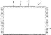
これらの図に示す半導体パッケージ1は、素子搭載用の回路基材としてリードフレーム2を具備している。リードフレーム2は図5に示すように、リード部3と素子支持部4とを備えている。リード部3は、リードフレーム2に搭載される半導体素子との接続部となるインナーリード5と、外部接続端子となるアウターリード6とを有し、複数のリードで構成されている。図4および図5ではアウターリード6の図示を一部省略しているが、図6に示すようにアウターリード6は外方に向けて突出している。 A semiconductor package 1 shown in these drawings includes a
リードフレーム2は下面側の第1の主面2aと上面側の第2の主面2bとを有している。半導体素子7は図2、図4および図7に示すように、リードフレーム2の下面(第1の主面)2a側に搭載されている。図4ないし図6はリードフレーム2の下面2aを示している。図7は半導体パッケージ1を反転させた状態、すなわちリードフレーム2の下面2aを上側に向けた状態を示している。ここで、リードフレーム2の下面および上面とは、アウターリード6を実装ボード等に接続した状態を基準とし、実装ボードの表面と対向する面を下面2a、実装ボードと対向する面とは反対側の面を上面2bとする。 The
リードフレーム2の下面2a側には、第1の半導体素子7A、第2の半導体素子7B、第3の半導体素子7Cおよび第4の半導体素子7Dが順に積層されて搭載されている。第1ないし第4の半導体素子7A、7B、7C、7Dの具体例としては、例えばNAND型フラッシュメモリのような半導体メモリ素子が挙げられる。半導体素子7の搭載数は複数個(少なくとも2個)であればよく、4個に限られるものではない。半導体パッケージ1に収納する半導体素子7の数は2個、3個もしくは5個以上であってもよい。 On the
第1の半導体素子7Aは第1の電極パッド8Aが形成された電極形成面9Aを有している。第1の半導体素子7Aは電極形成面9Aを下方(リードフレーム2の下面2aに対応する方向)に向けて、リードフレーム2の下面2a側に第1の接着層10を介して接着されている。後に詳述するように、インナーリード5は半導体素子7の短辺側に配置されたアウターリード6から半導体素子7のパッド配列辺(長辺)に向けて引き回されているため、第1の半導体素子7Aは素子支持部4に加えて、インナーリード5の一部に第1の接着層10を介して接着されている。 The
第1の接着層10には一般的なダイボンディング材、例えばシリコーン樹脂のような接着性を有する絶縁樹脂が用いられる。第1の接着層10の厚さは20〜30μmの範囲とすることが好ましい。第1の接着層10の厚さが20μm未満であると、リードフレーム2と第1の半導体素子7Aとの間の絶縁性を十分に確保することができないおそれがある。第1の接着層10の厚さが30μmを超えると半導体素子7の積層厚が厚くなる。 For the first
第2ないし第4の半導体素子7B、7C、7Dも、同様に第2ないし第4の電極パッド8B、8C、8Dが形成された電極形成面9B、9C、9Dを有している。第2の半導体素子7Bは電極形成面9Bを下方に向けて、第1の半導体素子7Aの電極形成面9Aに第2の接着層11を介して接着されている。同様に、第3および第4の半導体素子7C、7Dはそれぞれ電極形成面9C、9Dを下方に向け、第3の半導体素子7Cは第2の半導体素子7Bの電極形成面9Bに、また第4の半導体素子7Dは第3の半導体素子7Cの電極形成面9Cにそれぞれ第3および第4の接着層12、13を介して接着されている。 Similarly, the second to
第1ないし第4の半導体素子7A、7B、7C、7Dは矩形状でかつ同一の形状を有し、それぞれ長辺および短辺を揃えて積層されている。すなわち、リードフレーム2に対する半導体素子7A、7B、7C、7Dの占有面積(積層後の素子占有面積)が最小面積(1個の半導体素子7の面積に相当)となるように、第1ないし第4の半導体素子7A、7B、7C、7Dはそれぞれ各辺を揃えて積層されている。これによって、大型の半導体素子7を収容した場合のパッケージサイズの増大を抑制している。 The first to
第1ないし第4の半導体素子7A、7B、7C、7Dの電極パッド8A、8B、8C、8Dは、それぞれインナーリード5と第1ないし第4の金属ワイヤ14A、14B、14C、14Cを介して電気的に接続されている。金属ワイヤ14には一般的なAuワイヤやCuワイヤ等の金属細線が用いられる。金属ワイヤ14はループ高さを低減することが可能な逆ボンディングを適用してワイヤボンディングすることが好ましい。すなわち、電極パッド8上に予め金属バンプを形成しておき、金属ワイヤ14の一端をインナーリード5にボール接続し、他端を電極パッド8上に形成された金属バンプに接続する。 The
第1ないし第4の半導体素子7A、7B、7C、7Dは各辺を揃えて積層されているため、第1ないし第3の半導体素子7A、7B、7Cに接続された第1ないし第3の金属ワイヤ14A、14B、14Cにはそれぞれ下方(図7では上側)に配置された半導体素子7が干渉し、ショート等の不具合が発生するおそれがある。そこで、第1の金属ワイヤ14Aの第1の電極パッド8Aとの接続側端部(素子側端部)は、第2の接着層11内に埋め込まれている。同様に、第2および第3の金属ワイヤ14B、14Cの素子側端部は、それぞれ下方に位置する第3および第4の接着層12、13内に埋め込まれている。 Since the first to
このように、最下段の第4の半導体素子7Dを除いて、各半導体素子7A、7B、7Cに接続された金属ワイヤ14A、14B、14Cの素子側端部を、下方に位置する接着層11、12、13内に埋めこむことによって、第1の金属ワイヤ14Aと第2の半導体素子7Bとの接触、第2の金属ワイヤ14Bと第3の半導体素子7Cとの接触、第3の金属ワイヤ14Cと第4の半導体素子7Dとの接触を防止することができる。金属ワイヤ14は接着層11、12、13の厚さに基づいて半導体素子7から離間している。第2ないし第4の接着層11、12、13はスペーサ層としての機能を併せ持つものである。 Thus, except for the lowermost
スペーサ層として機能する第2ないし第4の接着層11、12、13は、接着機能を有することに加えて、半導体素子7の接着温度で軟化して金属ワイヤ14を内部に取り込むことが可能な絶縁樹脂で構成される。このような絶縁樹脂としては、例えばアクリル樹脂のような熱可塑性樹脂、あるいはエポキシ樹脂のような熱硬化性樹脂が挙げられる。接着層11、12、13の厚さは30〜100μmの範囲とすることが好ましく、さらに好ましくは50〜85μmの範囲である。接着層11、12、13の厚さが30μm未満の場合、金属ワイヤ14の半導体素子7との接触を抑制できないおそれがある。接着層11、12、13の厚さが100μmを超えると、半導体素子7の積層厚が厚くなりすぎる。 The second to fourth
各半導体素子7A、7B、7C、7Dの厚さは必ずしも限定されるものではないが、ワイヤボンディング時には最下段に位置することになる第1の半導体素子7Aの厚さは、他の半導体素子7B、7C、7Dの厚さより厚くすることが好ましい。具体的には、第1の半導体素子7Aの厚さは第1の接着層10の厚さと合計して100μm以上とすることが好ましい。ただし、第1の半導体素子7Aの厚さを厚くしすぎても積層厚が厚くなるだけであるため、第1の接着層10の厚さと合計して150μm以下とすることが好ましい。 The thickness of each of the
第1の半導体素子7Aの厚さが第1の接着層10の厚さと合計して100μm未満であると、ワイヤボンディング時にダメージを受けるおそれがある。第1の半導体素子7Aの厚さは80〜100μmの範囲とすることがより好ましい。他の半導体素子7B、7C、7Dは、ワイヤボンディング時には下方に位置する接着層11、12、13でボンディングダメージが緩和されるため、それらの厚さを薄くしてもダメージを受けるおそれはなく、逆に積層厚の増加を抑制する上で薄くすることが好ましい。 If the thickness of the
第2ないし第4の半導体素子7B、7C、7Dの厚さは、積層厚の増加を抑制する上で80μm未満とすることが好ましく、さらに70μm以下とすることが望ましい。第2ないし第4の半導体素子7B、7C、7Dの厚さの下限値は、特に限定されるものではなく、半導体素子の一般的な製造工程で作製が可能な範囲内(例えば20μm以上)で薄くすることが好ましい。第2ないし第4の半導体素子7B、7C、7Dの厚さは、実用的には50μm以上とすることが好ましい。いずれの厚さを選択した場合にも、第1の半導体素子7Aの厚さを他の半導体素子7B、7C、7Dの厚さより厚くすることが好ましい。 The thickness of the second to
リードフレーム2の下面2a側に積層されて搭載された第1ないし第4の半導体素子7A、7B、7C、7Dは、インナーリード5や第1ないし第4の金属ワイヤ14A、14B、14C、14Dと共に樹脂封止部15で封止されている。樹脂封止部15には一般的なエポキシ樹脂等が用いられる。これらによって、片面積層構造の半導体パッケージ1が構成されている。第1の実施形態の半導体パッケージ1は、半導体メモリ素子を多段に積層して高容量化を図った半導体記憶装置に好適である。 The first to
上述したように、第1ないし第4の半導体素子7A、7B、7C、7Dは、リードフレーム2の片面(下面2a)に積層されて搭載されている。このため、半導体パッケージ1の厚さ内に半導体素子7の積層厚を収容するために、リードフレーム2の素子支持部4からインナーリード5までを平坦化し、その上で素子支持部4とインナーリード5とによる平坦部を樹脂封止部15の上方側に配置している。言い換えると、リードフレーム2の下側の空間を確保するように、リードフレーム2の樹脂封止部15からの突出部(リードの肩口)を通常より上側に位置させている。 As described above, the first to
具体的には図3に示すように、リードフレーム2の上面2bから樹脂封止部15の上部までの厚さ(上側樹脂厚)T1を薄くし、リードフレーム2の下面2aから樹脂封止部15の下部までの厚さ(下側樹脂厚)T2を厚くしている。このような構成を適用することによって、リードフレーム2にディプレス加工を施すことなく、リードフレーム2の片面(下面2a)のみに半導体素子7を多段に積層して搭載することが可能となる。 Specifically, as shown in FIG. 3, the thickness (upper resin thickness) T1 from the
例えば、リードフレーム2の厚さを125μm、第1の半導体素子7Aと第1の接着層10との合計厚を110μm(素子厚85μm+接着層厚25μm)、第2ないし第4の半導体素子7B、7C、7Dの各厚さを70μm、第2ないし第4の接着層11、12、13の各厚さを60μm、樹脂封止部15の厚さを1000μm(1mm)としたとき、樹脂封止部15の上側樹脂厚T1を185μm、下側樹脂厚T2を690μmとする。 For example, the thickness of the
このような構成を採用することによって、多段に積層した半導体素子7(積層厚=400μm)を、ディプレス加工を施していないリードフレーム2の片面(下面2a)のみに搭載することが可能となる。さらに、リードフレーム2の樹脂封止部15からの突出部(リードの肩口)の位置を上側に設定することによって、アウターリード6の高さが高くなる。これによって、半導体パッケージ1を実装ボード等に実装した際のアウターリード6のバネ性が大きくなるため、半導体パッケージ1の実装信頼性、特に温度サイクルに対する信頼性(寿命)を向上させることができる。 By adopting such a configuration, it becomes possible to mount the multi-layered semiconductor elements 7 (lamination thickness = 400 μm) only on one side (
さらに、リードフレーム2の半導体素子7と対向する部分(素子支持部4とインナーリード5)を平坦化しているため、樹脂封止部15の大きさを同一とした場合で比較すると、リードフレーム2にディプレス加工を施した場合に比べて、リードフレーム2に搭載可能な半導体素子7のサイズを大きくすることができる。複数の半導体素子7の各辺を揃えて積層することによっても、リードフレーム2に搭載可能な素子サイズが増大する。これらによって、素子サイズが大きい半導体素子7の搭載が可能となる。 Furthermore, since the portion (element support portion 4 and inner lead 5) facing the
次に、半導体素子7のパッド配列構造とリードフレーム2の具体的な形状について述べる。第1ないし第4の電極パッド8A、8B、8C、8Dは、それぞれ第1ないし第4の半導体素子7A、7B、7C、7Dの外形の一辺、具体的に一方の長辺に沿って配列されている。すなわち、第1ないし第4の半導体素子7A、7B、7C、7Dは、図4に示すように長辺片側パッド構造を有している。一方、アウターリード6は半導体素子7の対向する短辺からそれぞれ突出するように配置されている。アウターリード6は半導体パッケージ1の両短辺からそれぞれ突出している。 Next, the pad arrangement structure of the
このため、リードフレーム2はアウターリード6を両短辺側に配置し、インナーリード5のボンディング部分を長辺側に配置する必要がある。そこで、インナーリード5はアウターリード6から半導体素子7との接続位置(半導体素子7の一方の長辺に対応する位置)に向けて引き回されている。具体的には、インナーリード5は短辺側に位置するアウターリード6と接続された部分から90度向きを変えるように、例えば約45度の方向に2回屈曲させて長辺側に引き回されている。このようなリードフレーム2を用いることによって、両短辺からアウターリード6を突出させた半導体パッケージ1に長辺片側パッド構造の半導体素子7を収容することが可能となる。 For this reason, in the
長辺片側パッド構造の半導体素子7は、短辺両側パッド構造の半導体素子や短辺片側パッド構造の半導体素子に比べて、素子サイズが制約されにくく、かつ接続電極数を多ピン化することができる。短辺両側パッド構造はリードフレーム2の形状を簡易化できるものの、長辺側の素子サイズが制約される。また、短辺片側パッド構造は長辺片側パッド構造に比べて接続電極数が制約される。このように、インナーリード5を引き回したリードフレーム2と長辺片側パッド構造の半導体素子7とを組合せることによって、大型で接続電極数が多い半導体素子7をリードフレーム2に搭載することが可能となる。 The
インナーリード5は短辺側から長辺側に引き回されているため、半導体素子7との接続部分側が動きやすい。そこで、インナーリード5の半導体素子7との接続部分の近傍を絶縁テープ16で固定している。これによって、インナーリード5に対するボンディング性やリードフレーム2の取り扱い性を高めている。インナーリード5を約45度の方向に2回屈曲させて生じた空間に、リードフレーム2の対向する二辺(ここでは対向する長辺)のそれぞれと連結された素子支持部4を配置している。これによって、リードフレーム2による半導体素子7の支持性を高めている。素子支持部4は貫通孔17を設けることで、接着層10に対する濡れ性を向上させている。 Since the
リードフレーム2はインナーリード5を短辺側から長辺側に引き回したことによって、インナーリード5の一部がリードフレーム2に搭載した半導体素子7と対向している。このような構造を有するリードフレーム2の両面に半導体素子を搭載すると、半導体素子に挟まれたリードフレーム2の隙間部分に封止樹脂を十分に充填することができないという問題が生じる。これに対して、半導体素子7はリードフレーム2の片面のみに搭載されているため、リードフレーム2の隙間部分にも封止樹脂を十分に充填することができる。これによって、封止信頼性に優れた半導体パッケージ1を提供することが可能となる。 In the
なお、図4における金属ワイヤ18は、インナーリード5の本数に対してアウターリード6の本数が多い場合の分岐用ワイヤである。例えば、半導体素子7の電極(チップイネーブル等)が2個であるのに対し、半導体パッケージ1としては4個の電極が必要な場合、インナーリード5で分岐(複数点へのワイヤボンディングと引き回し)できれば問題はないが、それができない場合に引戻し用のインナーリード5を配置し、これと増加分のアウターリード6とを金属ワイヤ18で接続している。このような構造を適用することによって、各種の電極配置構造に適用することが可能となる。 Note that the
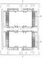
次に、本発明の第2の実施形態による半導体パッケージについて、図8ないし図14を参照して説明する。図8は第2の実施形態による半導体パッケージの平面構造を示している。図9は第1の素子群のワイヤボンディング構造、図10は第2の素子群のワイヤボンディング構造を示している。図11および図12は半導体パッケージの断面構造を示している。図13は各半導体素子に対する具体的なワイヤボンディング状態を示しており、図14はその変形例を示している。なお、図8は樹脂封止部の図示を省略している。 Next, a semiconductor package according to a second embodiment of the present invention will be described with reference to FIGS. FIG. 8 shows a planar structure of the semiconductor package according to the second embodiment. FIG. 9 shows the wire bonding structure of the first element group, and FIG. 10 shows the wire bonding structure of the second element group. 11 and 12 show a cross-sectional structure of the semiconductor package. FIG. 13 shows a specific wire bonding state for each semiconductor element, and FIG. 14 shows a modification thereof. In FIG. 8, illustration of the resin sealing portion is omitted.
これらの図に示す半導体パッケージ21は、素子搭載用の回路基材として配線基板22を有している。回路基材は半導体素子を搭載することが可能で、かつ回路部を有するものであればよく、配線基板22に代えて第1の実施形態と同様にリードフレームを適用することも可能である。配線基板22は、例えば絶縁樹脂基板の内部や表面に配線網を設けたものであり、具体的にはガラス−エポキシ樹脂やBT樹脂(ビスマレイミド・トリアジン樹脂)等を使用したプリント配線基板が適用される。 The
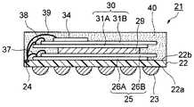
配線基板22の下面側の第1の主面22aには、外部接続端子23として半田バンプ等が設けられている。ここではBGAパッケージに適用する半導体パッケージ21を示しているため、配線基板22の下面に外部接続端子23として半田バンプを設けている。半導体パッケージ21はLGAパッケージ等にも適用可能であり、この場合には外部接続端子23として金属ランドが適用される。配線基板22の上面側の第2の主面22bには、素子搭載部と接続パッド24とが設けられている。接続パッド24は配線基板22の配線網を介して外部接続端子23と電気的に接続されている。接続パッド24はワイヤボンディング時の接続部となるものである。 On the first
配線基板22の素子搭載部上には、第1の素子群25を構成する第1および第2の半導体素子26A、26Bが順に積層されている。第1の半導体素子26Aは図示を省略した接着層を介して素子搭載部上に接着されており、第2の半導体素子26Bは図示を省略した接着層を介して第1の半導体素子26A上に接着されている。これら半導体素子26A、26Bは矩形状で同一の形状を有している。第1および第2の半導体素子26A、26Bはそれぞれ第1および第2の電極パッド27A、27Bが形成された電極形成面28A、28Bを有し、電極形成面28A、28Bを上方に向けて配置されている。 On the element mounting portion of the
第1の素子群25上にはスペーサ層29を介して第2の素子群30を構成する第3および第4の半導体素子31A、31Bが順に積層されている。スペーサ層29は、例えば図示を省略した接着層を介して第2の半導体素子26B上に接着されている。第3の半導体素子31Aは図示を省略した接着層を介してスペーサ層29上に接着されており、第4の半導体素子31Bは図示を省略した接着層を介して第3の半導体素子31A上に接着されている。なお、後に詳述するように、スペーサ層29に接着性を有する絶縁樹脂層を適用した場合には、スペーサ層29や第3の半導体素子31Aの接着層は省略される。 On the
第3および第4の半導体素子31A、31Bは矩形状でかつ同一の形状を有している。これら半導体素子31A、31Bはそれぞれ第3および第4の電極パッド32A、32Bが形成された電極形成面33A、33Bを有し、電極形成面33A、33Bを上方に向けて配置されている。第4の半導体素子31B上には第5の半導体素子34が積層されている。第5の半導体素子34は図示を省略した接着層を介して第4の半導体素子31B上に接着されている。第5の半導体素子34は他の半導体素子に比べて小形の形状を有している。第5の半導体素子34は第2の素子群30の一部を構成するものであってもよい。 The third and
第1ないし第4の半導体素子26A、26B、31A、31Bの具体例としては、例えばNAND型フラッシュメモリのような半導体メモリ素子が挙げられる。また、第5の半導体素子34の具体例としては、例えば半導体メモリ素子のコントローラ素子が挙げられる。第1および第2の素子群25、30を構成する半導体素子26、31の数は、それぞれ複数個(少なくとも2個)であればよく、2個もしくは3個に限られるものではない。第1の素子群25は3個以上の半導体素子26で構成してもよい。また、第2の素子群30は2個もしくは4個以上の半導体素子31、34で構成してもよい。 Specific examples of the first to
第1ないし第4の電極パッド27A、27B、32A、32Bは、それぞれ第1ないし第4の半導体素子26A、26B、31A、31Bの外形の一辺、具体的には一方の長辺に沿って配列されている。すなわち、第1ないし第4の半導体素子26A、26B、31A、31Bはそれぞれ長辺片側パッド構造を有している。第5の半導体素子34は隣接する二辺に沿って配列された電極パッド35を有している。第5の半導体素子34はL型パッド構造を有している。第5の半導体素子34は他の半導体素子と同様に、電極パッド35が形成された電極形成面36を上方に向けて配置されている。 The first to
長辺片側パッド構造を有する第1および第2の半導体素子26A、26Bは、各電極パッド27A、27Bが露出するように階段状に積層されている。すなわち、第1および第2の半導体素子26A、26Bの短辺を揃え、かつ長辺を第1の電極パッド27Aが露出するようにずらして積層されている。第2の電極パッド27Bは、第1の素子群25と第2の素子群30との間にスペーサ層29を配置することで露出されている。 The first and
同様に、第3および第4の半導体素子31A、31Bは、各電極パッド32A、32Bが露出するように階段状に積層されている。すなわち、第3および第4の半導体素子31A、31Bの短辺を揃え、かつ長辺を第3の電極パッド32Aが露出するようにずらして積層されている。第5の半導体素子34は他の半導体素子より小形であるため、第4の半導体素子31B上に第5の半導体素子34が積層されているものの、そのままの状態で第4の電極パッド32Bは露出されている。 Similarly, the third and
第1ないし第4の半導体素子26A、26B、31A、31Bは、それぞれ短辺を揃え、かつ第1の半導体素子26Aと第3の半導体素子31Aの長辺、および第2の半導体素子26Bと第4の半導体素子31Bの長辺を揃えて積層されている。このような積層構造を適用することによって、各電極パッド27A、27B、32A、32Bを露出させた上で、配線基板22に対する半導体素子26、31の占有面積の増大を抑制している。すなわち、4個の半導体素子を全て階段状に積層した場合、半導体素子の占有面積は1個の半導体素子の面積に3個分のずらした面積を加えた面積となる。 The first to
これに対し、この実施形態の素子占有面積は1個の半導体素子の面積に1個分のずらした面積を加えた面積となる。このように、複数の半導体素子を第1の素子群25と第2の素子群30とに分け、第1の素子群25と第2の素子群30との間にスペーサ層29を配置する共に、各素子群25、30内の半導体素子を階段状に積層し、その上で各素子群25、30の配置を揃えることによって、1個のスペーサ層29で各電極パッド27A、27B、32A、32Bを露出させた上で、配線基板22に対する半導体素子の占有面積の増大を抑制することができる。スペーサ層29の増加は積層厚の増大に繋がる。従って、薄型でかつ面積の増大を抑制した半導体パッケージ21を提供することが可能となる。 On the other hand, the element occupation area of this embodiment is an area obtained by adding one shifted area to the area of one semiconductor element. As described above, the plurality of semiconductor elements are divided into the
第1および第2の半導体素子26A、26Bの第1および第2の電極パッド27A、27Bは、配線基板22の接続パッド24と第1の金属ワイヤ37を介して電気的に接続されている。第1の電極パッド27Aと第2の電極パッド27Bの電気特性や信号特性等が等しい場合には、第2の電極パッド27Bに接続された金属ワイヤ37を第1の電極パッド27Aに接続し、この第1の電極パッド27Aを介して接続パッド24と第2の接続パッド27Bとを電気的に接続することができる。この場合の金属ワイヤ37は個々にボンディンク工程を実施して接続してもよいし、1本の金属ワイヤ37で接続パッド24と第1の電極パッド27Aと第2の電極パッド27Bとを順に接続してもよい。 The first and
第3および第4の半導体素子31A、31Bの電極パッド32A、32Bは、同様に配線基板22の接続パッド24と第2の金属ワイヤ38を介して電気的に接続されている。第2の素子群30についても、第1の素子群25と同様な接続構造が適用される。第5の半導体素子34の電極パッド35は、配線基板22の接続パッド24と第3の金属ワイヤ39を介して電気的に接続されている。金属ワイヤ37、38、39は一般的なAuワイヤやCuワイヤ等の金属細線で構成される。金属ワイヤ37、38、39にはループ高さを低減することが可能な逆ボンディングを適用することが好ましい。 Similarly, the
半導体素子26、31、34が実装された配線基板22の第2の主面22bには、例えばエポキシ樹脂からなる樹脂封止部40がモールド成形されている。半導体素子26、31、34は、金属ワイヤ37、38、39等と共に樹脂封止部40で一体的に封止されている。これらによって、BGAやLGA等として用いられる片面積層構造の半導体パッケージ21が構成されている。第2の実施形態の半導体パッケージ21は、半導体メモリ素子を多段に積層して高容量化を図った半導体記憶装置に好適である。 A
各素子群25、30を構成する半導体素子26、31の厚さは必ずしも限定されるものではないが、それぞれ下段側の半導体素子26A、31Aの厚さを上段側の半導体素子26B、31Bの厚さより厚くすることが好ましい。第1の素子群25に関しては、第1の半導体素子26Aはワイヤボンディング時にダメージを受けやすいと共に、配線基板22の表面凹凸に起因して樹脂封止部40のモールド成形時に割れが生じるおそれがあることから、その厚さは80〜150μmの範囲とすることが好ましい。 The thicknesses of the semiconductor elements 26 and 31 constituting the
第2の素子群30に関しては、第3の半導体素子31Aはボンディング部がオーバーハング状態となっており、その部分が撓むとワイヤボンディング性が低下するため、その厚さは100〜180μmの範囲とすることが好ましい。第2および第4の半導体素子26B、31Bの厚さは積層厚の増加を抑制する上で、それぞれ80μm未満とすることが好ましく、さらに70μm以下とすることが望ましい。これら半導体素子26B、31Bの厚さの下限値は第1の実施形態と同様である。第5の半導体素子34の厚さは機能や積層厚の観点から適宜に選択される。 Regarding the
第1の素子群25と第2の素子群30との間に配置されるスペーサ層は、図14に示すように、金属ワイヤ37の素子側端部を取り込むことが可能な絶縁樹脂層41で構成してもよい。絶縁樹脂層41はスペーサ層としての機能に加えて、接着層としての機能を併せ持つものである。絶縁樹脂層41は、例えばアクリル樹脂のような熱可塑性樹脂、あるいはエポキシ樹脂のような熱硬化性樹脂で構成され、その厚さは30〜120μmの範囲とすることが好ましく、さらに好ましくは50〜100μmの範囲である。 As shown in FIG. 14, the spacer layer disposed between the
なお、本発明は上記した各実施形態に限定されるものではなく、複数の半導体素子をリードフレーム等の回路基材の片面に積層して搭載した各種の半導体パッケージに適用することができる。そのような半導体パッケージも本発明に含まれるものである。また、本発明の実施形態は本発明の技術的思想の範囲内で拡張もしくは変更することができ、この拡張、変更した実施形態も本発明の技術的範囲に含まれるものである。 The present invention is not limited to the above-described embodiments, and can be applied to various semiconductor packages in which a plurality of semiconductor elements are stacked and mounted on one side of a circuit substrate such as a lead frame. Such a semiconductor package is also included in the present invention. The embodiments of the present invention can be expanded or modified within the scope of the technical idea of the present invention, and the expanded and modified embodiments are also included in the technical scope of the present invention.
1,21…半導体パッケージ、2…リードフレーム、3…リード部、4…素子支持部、5…インナーリード、6…アウターリード、7,26,31…半導体素子、7A,26A…第1の半導体素子、7B,26B…第2の半導体素子、7C,31A…第3の半導体素子、7D,31B…第4の半導体素子、8,8A,8B,8C,8D,27A,27B,32A,32B,35…電極パッド、9,9A,9B,9C,9D,28A,28B,33A,33B,36…電極形成面、10…第1の接着層、11…第2の接着層、12…第3の接着層、13…第4の接着層、14…金属ワイヤ、14A,37…第1の金属ワイヤ、14B,38…第2の金属ワイヤ、14C,39…第3の金属ワイヤ、14D…第4の金属ワイヤ、15,40…樹脂封止部、22…配線基板、24…接続パッド、25…第1の素子群、29…スペーサ層、30…第2の素子群。 DESCRIPTION OF
Claims (2)
Translated fromJapanese第1の電極パッドが形成された第1の電極形成面を有し、前記第1の電極形成面を下方に向けて前記リードフレームの下面側に第1の接着層を介して接着された第1の半導体素子と、
第2の電極パッドが形成された第2の電極形成面を有し、前記第2の電極形成面を下方に向けて前記第1の半導体素子の第1の電極形成面に第2の接着層を介して接着された第2の半導体素子と、
前記インナーリードと前記第1の電極パッドとに接続され、前記第1の半導体素子との接続側端部が前記第2の接着層内に埋め込まれた第1の金属ワイヤと、
前記インナーリードと前記第2の電極パッドとに接続された第2の金属ワイヤと、
前記第1および第2の半導体素子を前記第1および第2の金属ワイヤと共に封止する樹脂封止部とを具備し、
前記第1および第2の前記電極パッドはそれぞれ前記第1および第2の半導体素子の片側の長辺に沿って配列されており、
かつ、前記アウターリードは前記第1および第2の半導体素子の対向する短辺からそれぞれ突出するように配置されていると共に、前記インナーリードは前記アウターリードから前記第1および第2の電極パッドが配列された前記第1および第2の半導体素子の長辺に向けて引き回されていることを特徴とする半導体パッケージ。Alead frame comprising an element support and a lead part having an inner lead and an outer lead; and a flatlead frame from the element support to the inner lead;
A first electrode forming surface on which a first electrode pad is formed, and the first electrode forming surface is directed downward and bonded to the lower surface side of thelead frame via a first adhesive layer; 1 semiconductor element;
A second adhesive layer on the first electrode forming surface of the first semiconductor element, the second electrode forming surface having a second electrode pad formed thereon, the second electrode forming surface facing downward; A second semiconductor element bonded via
A first metal wire connected to the inner lead and the first electrode pad and having a connection-side end with the first semiconductor element embedded in the second adhesive layer;
A second metal wire connected to the inner lead and the second electrode pad;
A resin sealing portion that seals the first and second semiconductor elements together with the first and second metal wires;
The first and second electrode pads are arranged along the long sides on one side of the first and second semiconductor elements, respectively.
The outer leads are arranged so as to protrude from the opposing short sides of the first and second semiconductor elements, respectively, and the inner leads are connected to the first and second electrode pads from the outer leads. A semiconductor package characterized by being routed toward the long sides of the arranged first and second semiconductor elements.
さらに、第3の電極パッドが形成された第3の電極形成面を有し、前記第3の電極形成面を下方に向けて前記第2の半導体素子の第2の電極形成面に第3の接着層を介して接着された第3の半導体素子と、
第4の電極パッドが形成された第4の電極形成面を有し、前記第4の電極形成面を下方に向けて前記第3の半導体素子の第3の電極形成面に第4の接着層を介して接着された第4の半導体素子と、
前記インナーリードと前記第3の電極パッドとに接続された第3の金属ワイヤと、
前記インナーリードと前記第4の電極パッドとに接続された第4の金属ワイヤとを具備し、
前記第2の金属ワイヤの前記第2の半導体素子との接続側端部は前記第3の接着層内に埋め込まれており、かつ前記第3の金属ワイヤの前記第3の半導体素子との接続側端部は前記第4の接着層内に埋め込まれており、
前記第3および第4の電極パッドはそれぞれ前記第3および第4の半導体素子の片側の長辺に沿って配列されていることを特徴とする半導体パッケージ。The semiconductor package according to claim 1,
And a third electrode forming surface on which a third electrode pad is formed. The third electrode forming surface faces downward and a third electrode forming surface is formed on the second electrode forming surface of the second semiconductor element. A third semiconductor element bonded via an adhesive layer;
A fourth adhesive layer on the third electrode formation surface of the third semiconductor element having a fourth electrode formation surface on which a fourth electrode pad is formed, with the fourth electrode formation surface facing downward; A fourth semiconductor element bonded via
A third metal wire connected to the inner lead and the third electrode pad;
A fourth metal wire connected to the inner lead and the fourth electrode pad;
A connection side end portion of the second metal wire with the second semiconductor element is embedded in the third adhesive layer, and the connection of the third metal wire with the third semiconductor element is performed. Side edges are embedded in the fourth adhesive layer;
3. The semiconductor package according to claim 1, wherein the third and fourth electrode pads are arranged along one long side of each of the third and fourth semiconductor elements.
Priority Applications (6)
| Application Number | Priority Date | Filing Date | Title |
|---|---|---|---|
| JP2007119798AJP4489094B2 (en) | 2007-04-27 | 2007-04-27 | Semiconductor package |
| TW097114533ATWI363417B (en) | 2007-04-27 | 2008-04-21 | Semiconductor device |
| TW101123783ATWI515871B (en) | 2007-04-27 | 2008-04-21 | Lead frame |
| TW101100070ATWI397167B (en) | 2007-04-27 | 2008-04-21 | Semiconductor device |
| US12/106,511US8022515B2 (en) | 2007-04-27 | 2008-04-21 | Semiconductor device |
| KR1020080038609AKR100947146B1 (en) | 2007-04-27 | 2008-04-25 | Semiconductor package |
Applications Claiming Priority (1)
| Application Number | Priority Date | Filing Date | Title |
|---|---|---|---|
| JP2007119798AJP4489094B2 (en) | 2007-04-27 | 2007-04-27 | Semiconductor package |
Publications (2)
| Publication Number | Publication Date |
|---|---|
| JP2008277571A JP2008277571A (en) | 2008-11-13 |
| JP4489094B2true JP4489094B2 (en) | 2010-06-23 |
Family
ID=39968764
Family Applications (1)
| Application Number | Title | Priority Date | Filing Date |
|---|---|---|---|
| JP2007119798AActiveJP4489094B2 (en) | 2007-04-27 | 2007-04-27 | Semiconductor package |
Country Status (4)
| Country | Link |
|---|---|
| US (1) | US8022515B2 (en) |
| JP (1) | JP4489094B2 (en) |
| KR (1) | KR100947146B1 (en) |
| TW (3) | TWI515871B (en) |
Families Citing this family (2)
| Publication number | Priority date | Publication date | Assignee | Title |
|---|---|---|---|---|
| JP4489100B2 (en) | 2007-06-18 | 2010-06-23 | 株式会社東芝 | Semiconductor package |
| US8680686B2 (en)* | 2010-06-29 | 2014-03-25 | Spansion Llc | Method and system for thin multi chip stack package with film on wire and copper wire |
Family Cites Families (29)
| Publication number | Priority date | Publication date | Assignee | Title |
|---|---|---|---|---|
| US4891687A (en)* | 1987-01-12 | 1990-01-02 | Intel Corporation | Multi-layer molded plastic IC package |
| US5340771A (en)* | 1993-03-18 | 1994-08-23 | Lsi Logic Corporation | Techniques for providing high I/O count connections to semiconductor dies |
| JPH08279591A (en)* | 1995-04-07 | 1996-10-22 | Nec Corp | Semiconductor device and its manufacture |
| US6057598A (en)* | 1997-01-31 | 2000-05-02 | Vlsi Technology, Inc. | Face on face flip chip integration |
| US5986209A (en)* | 1997-07-09 | 1999-11-16 | Micron Technology, Inc. | Package stack via bottom leaded plastic (BLP) packaging |
| JPH1168015A (en)* | 1997-08-12 | 1999-03-09 | Hitachi Ltd | Lead frame, semiconductor device using the same, and method of manufacturing the same |
| US6034423A (en)* | 1998-04-02 | 2000-03-07 | National Semiconductor Corporation | Lead frame design for increased chip pinout |
| US6278616B1 (en)* | 1998-07-07 | 2001-08-21 | Texas Instruments Incorporated | Modifying memory device organization in high density packages |
| JP3494901B2 (en)* | 1998-09-18 | 2004-02-09 | シャープ株式会社 | Semiconductor integrated circuit device |
| US6667541B1 (en)* | 1998-10-21 | 2003-12-23 | Matsushita Electric Industrial Co., Ltd. | Terminal land frame and method for manufacturing the same |
| TW423124B (en)* | 1998-11-27 | 2001-02-21 | Walsin Advanced Electronics | Lead frame with heat dissipation plate |
| US6424541B1 (en)* | 1999-04-21 | 2002-07-23 | Conexant Systems, Inc | Electronic device attachment methods and apparatus for forming an assembly |
| TW463346B (en)* | 1999-05-04 | 2001-11-11 | Sitron Prec Co Ltd | Dual-leadframe package structure and its manufacturing method |
| US6256200B1 (en)* | 1999-05-27 | 2001-07-03 | Allen K. Lam | Symmetrical package for semiconductor die |
| KR20010064907A (en)* | 1999-12-20 | 2001-07-11 | 마이클 디. 오브라이언 | wire bonding method and semiconductor package using it |
| KR100464561B1 (en) | 2000-04-11 | 2004-12-31 | 앰코 테크놀로지 코리아 주식회사 | Semiconductor package and manufacturing method the same |
| JP2001308262A (en)* | 2000-04-26 | 2001-11-02 | Mitsubishi Electric Corp | Resin-sealed BGA type semiconductor device |
| TW459361B (en)* | 2000-07-17 | 2001-10-11 | Siliconware Precision Industries Co Ltd | Three-dimensional multiple stacked-die packaging structure |
| JP3913481B2 (en) | 2001-01-24 | 2007-05-09 | シャープ株式会社 | Semiconductor device and manufacturing method of semiconductor device |
| US6388313B1 (en)* | 2001-01-30 | 2002-05-14 | Siliconware Precision Industries Co., Ltd. | Multi-chip module |
| US6555917B1 (en)* | 2001-10-09 | 2003-04-29 | Amkor Technology, Inc. | Semiconductor package having stacked semiconductor chips and method of making the same |
| US6737750B1 (en)* | 2001-12-07 | 2004-05-18 | Amkor Technology, Inc. | Structures for improving heat dissipation in stacked semiconductor packages |
| US7332819B2 (en)* | 2002-01-09 | 2008-02-19 | Micron Technology, Inc. | Stacked die in die BGA package |
| US6841858B2 (en)* | 2002-09-27 | 2005-01-11 | St Assembly Test Services Pte Ltd. | Leadframe for die stacking applications and related die stacking concepts |
| TWI280653B (en)* | 2004-12-01 | 2007-05-01 | Macronix Int Co Ltd | Package |
| US7163839B2 (en)* | 2005-04-27 | 2007-01-16 | Spansion Llc | Multi-chip module and method of manufacture |
| JP4674113B2 (en)* | 2005-05-06 | 2011-04-20 | Okiセミコンダクタ株式会社 | Semiconductor device and manufacturing method thereof |
| JP2007035865A (en) | 2005-07-26 | 2007-02-08 | Toshiba Corp | Semiconductor package and manufacturing method thereof |
| JP2007134486A (en) | 2005-11-10 | 2007-05-31 | Toshiba Corp | Multilayer semiconductor device and manufacturing method thereof |
- 2007
- 2007-04-27JPJP2007119798Apatent/JP4489094B2/enactiveActive
- 2008
- 2008-04-21USUS12/106,511patent/US8022515B2/enactiveActive
- 2008-04-21TWTW101123783Apatent/TWI515871B/enactive
- 2008-04-21TWTW097114533Apatent/TWI363417B/enactive
- 2008-04-21TWTW101100070Apatent/TWI397167B/enactive
- 2008-04-25KRKR1020080038609Apatent/KR100947146B1/enactiveActive
Also Published As
| Publication number | Publication date |
|---|---|
| JP2008277571A (en) | 2008-11-13 |
| TWI515871B (en) | 2016-01-01 |
| US8022515B2 (en) | 2011-09-20 |
| KR100947146B1 (en) | 2010-03-12 |
| TW201220466A (en) | 2012-05-16 |
| TW201246512A (en) | 2012-11-16 |
| TW200908284A (en) | 2009-02-16 |
| TWI397167B (en) | 2013-05-21 |
| TWI363417B (en) | 2012-05-01 |
| KR20080096442A (en) | 2008-10-30 |
| US20080277770A1 (en) | 2008-11-13 |
Similar Documents
| Publication | Publication Date | Title |
|---|---|---|
| JP4498403B2 (en) | Semiconductor device and semiconductor memory device | |
| JP4489100B2 (en) | Semiconductor package | |
| JP4751351B2 (en) | Semiconductor device and semiconductor module using the same | |
| JP4776675B2 (en) | Semiconductor memory card | |
| JP4322844B2 (en) | Semiconductor device and stacked semiconductor device | |
| US11688659B2 (en) | Method for manufacturing a semiconductor device having a semiconductor element mounted on a lead frame | |
| JP5150243B2 (en) | Semiconductor memory device | |
| JP2010177456A (en) | Semiconductor device | |
| JP2009158738A (en) | Semiconductor device and semiconductor memory device | |
| JP4489094B2 (en) | Semiconductor package | |
| JP5275019B2 (en) | Semiconductor device | |
| JP4602223B2 (en) | Semiconductor device and semiconductor package using the same | |
| JP2010232702A (en) | Multilayer semiconductor device | |
| US7847396B2 (en) | Semiconductor chip stack-type package and method of fabricating the same | |
| JP2009259940A (en) | Semiconductor package | |
| KR20100055853A (en) | Semiconductor package of multi stack type |
Legal Events
| Date | Code | Title | Description |
|---|---|---|---|
| A621 | Written request for application examination | Free format text:JAPANESE INTERMEDIATE CODE: A621 Effective date:20090311 | |
| A977 | Report on retrieval | Free format text:JAPANESE INTERMEDIATE CODE: A971007 Effective date:20090904 | |
| A131 | Notification of reasons for refusal | Free format text:JAPANESE INTERMEDIATE CODE: A131 Effective date:20090915 | |
| A521 | Request for written amendment filed | Free format text:JAPANESE INTERMEDIATE CODE: A523 Effective date:20091112 | |
| A131 | Notification of reasons for refusal | Free format text:JAPANESE INTERMEDIATE CODE: A131 Effective date:20091208 | |
| A521 | Request for written amendment filed | Free format text:JAPANESE INTERMEDIATE CODE: A523 Effective date:20100201 | |
| RD02 | Notification of acceptance of power of attorney | Free format text:JAPANESE INTERMEDIATE CODE: A7422 Effective date:20100201 | |
| TRDD | Decision of grant or rejection written | ||
| A01 | Written decision to grant a patent or to grant a registration (utility model) | Free format text:JAPANESE INTERMEDIATE CODE: A01 Effective date:20100302 | |
| A01 | Written decision to grant a patent or to grant a registration (utility model) | Free format text:JAPANESE INTERMEDIATE CODE: A01 | |
| A61 | First payment of annual fees (during grant procedure) | Free format text:JAPANESE INTERMEDIATE CODE: A61 Effective date:20100330 | |
| FPAY | Renewal fee payment (event date is renewal date of database) | Free format text:PAYMENT UNTIL: 20130409 Year of fee payment:3 | |
| R151 | Written notification of patent or utility model registration | Ref document number:4489094 Country of ref document:JP Free format text:JAPANESE INTERMEDIATE CODE: R151 | |
| FPAY | Renewal fee payment (event date is renewal date of database) | Free format text:PAYMENT UNTIL: 20130409 Year of fee payment:3 | |
| FPAY | Renewal fee payment (event date is renewal date of database) | Free format text:PAYMENT UNTIL: 20140409 Year of fee payment:4 | |
| S111 | Request for change of ownership or part of ownership | Free format text:JAPANESE INTERMEDIATE CODE: R313111 | |
| R350 | Written notification of registration of transfer | Free format text:JAPANESE INTERMEDIATE CODE: R350 | |
| S111 | Request for change of ownership or part of ownership | Free format text:JAPANESE INTERMEDIATE CODE: R313111 | |
| R350 | Written notification of registration of transfer | Free format text:JAPANESE INTERMEDIATE CODE: R350 |