JP4487900B2 - Image processing system - Google Patents
Image processing systemDownload PDFInfo
- Publication number
- JP4487900B2 JP4487900B2JP2005309781AJP2005309781AJP4487900B2JP 4487900 B2JP4487900 B2JP 4487900B2JP 2005309781 AJP2005309781 AJP 2005309781AJP 2005309781 AJP2005309781 AJP 2005309781AJP 4487900 B2JP4487900 B2JP 4487900B2
- Authority
- JP
- Japan
- Prior art keywords
- image
- block
- circuit
- class
- pixel
- Prior art date
- Legal status (The legal status is an assumption and is not a legal conclusion. Google has not performed a legal analysis and makes no representation as to the accuracy of the status listed.)
- Expired - Fee Related
Links
- 238000012545processingMethods0.000titleclaimsdescription135
- 238000013507mappingMethods0.000claimsdescription117
- 238000004364calculation methodMethods0.000claimsdescription75
- 238000012937correctionMethods0.000description133
- 230000000903blocking effectEffects0.000description64
- 238000000034methodMethods0.000description57
- 230000008569processEffects0.000description50
- 230000006835compressionEffects0.000description17
- 238000007906compressionMethods0.000description17
- 230000003044adaptive effectEffects0.000description15
- 230000006870functionEffects0.000description15
- 238000010586diagramMethods0.000description11
- 230000005540biological transmissionEffects0.000description10
- 239000000284extractSubstances0.000description4
- 239000011159matrix materialSubstances0.000description4
- 230000008859changeEffects0.000description3
- 238000013139quantizationMethods0.000description3
- 230000003287optical effectEffects0.000description2
- 230000009471actionEffects0.000description1
- 230000003247decreasing effectEffects0.000description1
- 230000001934delayEffects0.000description1
- 230000003111delayed effectEffects0.000description1
- 238000001514detection methodMethods0.000description1
- 230000006866deteriorationEffects0.000description1
- 230000000694effectsEffects0.000description1
- 230000008030eliminationEffects0.000description1
- 238000003379elimination reactionMethods0.000description1
- 230000002093peripheral effectEffects0.000description1
- 230000004044responseEffects0.000description1
- 238000012549trainingMethods0.000description1
Images


Landscapes
- Compression Or Coding Systems Of Tv Signals (AREA)
- Compression Of Band Width Or Redundancy In Fax (AREA)
- Compression, Expansion, Code Conversion, And Decoders (AREA)
Description
Translated fromJapanese本発明は、画像処理システムに関する。特に、原画像とほぼ同一の復号画像が得られるように、画像を間引いて圧縮符号化する画像処理システムに関する。The present invention relates to animage processing system . In particular, the present invention relates to animage processing system that performs compression encoding by thinning out images so that a decoded image that is substantially the same as an original image is obtained.
従来より、画像の圧縮方法については、種々の方法が提案されているが、そのうちの1つに、画像を、例えばその画素を間引くこと(Subsampling)により圧縮する方法がある。 Conventionally, various image compression methods have been proposed. One of them is a method of compressing an image, for example, by subsampling its pixels.
しかしながら、このように間引いて圧縮した画像を、単純に補間により伸張した場合、その結果得られる復号画像の解像度が劣化する。 However, when the thinned and compressed image is simply expanded by interpolation, the resolution of the resulting decoded image deteriorates.
ここで、このように復号画像の解像度が劣化する原因として、第1に、間引い画像には、元の画像に含まれる高周波数成分が含まれていないことと、第2に、間引き後の画像を構成する画素の画素値が、元の画像を復元するのに、必ずしも適当でないこととが考えられる。 Here, as a cause of the deterioration of the resolution of the decoded image in this way, first, the thinned image does not contain the high frequency component included in the original image, and secondly, the image after the thinning is performed. It is considered that the pixel values of the pixels constituting the are not necessarily suitable for restoring the original image.
本発明は、このような状況に鑑みてなされたものであり、原画像と同一(ほぼ同一)の復号画像が得られるように、画像を間引いて圧縮符号化することができるようにするものである。 The present invention has been made in view of such circumstances, and enables compression coding by thinning out an image so that a decoded image that is the same (substantially the same) as the original image is obtained. is there.
本発明の一側面の画像処理システムは、画像を符号化する画像符号化装置と、符号化された前記画像を復号化する画像復号化装置とからなる画像処理システムであって、前記画像符号化装置は、前記画像を構成する画素から注目している注目画素周辺の複数の画素を抽出し、抽出された前記複数の画素の性質に応じて前記注目画素を第1のクラスに分類する分類手段と、前記第1のクラスごとに、前記画像を符号化するための所定のマッピング係数を記憶しているマッピング係数記憶手段と、前記画像の中の、注目している前記注目画素周辺の複数の画素と、前記注目画素の第1のクラスに対応する前記マッピング係数とを引数とする所定の関数の演算を行うことにより、符号化された前記注目画素を、前記注目画素周辺の複数の画素の符号化データとして出力する演算手段とを備え、前記画像復号化装置は、前記画像符号化装置で符号化させた前記符号化データを受信する受信手段と、前記符号化データを復号化する復号化手段とを備え、前記復号化手段は、前記符号化データを、その性質に応じて第2のクラスのうちのいずれかに分類する分類手段と、前記符号化データの前記第2のクラスに対応する、前記符号化データから予測される元の画像の予測値を算出するための予測係数と、前記符号化データとの線形結合により、前記予測値を求める予測値演算手段とを有する。An image processing system according to one aspect of the present invention isan image processing system including an image encoding device that encodes an image and an image decoding device that decodes the encoded image. The apparatus extractsa plurality of pixels aroundthe target pixel of interest from the pixels constituting the image, and classifies the target pixel into a first class according to the properties of the extracted pixels Mapping coefficient storage means for storing a predetermined mapping coefficient for encoding the image for each of the first classes, anda plurality of pixels aroundthe target pixel of interest in the image By performing a predetermined function operation using a pixel and the mapping coefficient corresponding to the first class of the pixel of interest as an argument, theencoded pixel of interest is converted into a plurality of pixels around the pixel of interest. Sign Computing means for outputting as data, wherein the image decoding device comprises: receiving means for receiving the encoded data encoded by the image encoding device; and decoding means for decoding the encoded data; Thedecoding means corresponds to the second class of the encoded data, the classification means for classifying the encoded data into one of the second class according to the nature, A prediction value calculating unit that obtains the prediction value by linear combination of a prediction coefficient for calculating the prediction value of the original image predicted from the encoded data and the encoded data ;
前記演算手段は、符号化された前記注目画素を、前記注目画素周辺の複数の画素の前記符号化データとすることによって、前記画像の画素数を少なくしたものを算出するようにすることができる。The arithmetic means can calculate the image with a reduced number of pixels by using the encoded pixel of interest as the encoded data ofa plurality of pixels aroundthe pixel of interest. .
前記復号化手段は、
前記予測係数を、前記第2のクラスごとに記憶している予測係数記憶手段をさらに備えるようにすることができる。The decoding means includes
The prediction coefficients, it is possible tofurther include a prediction coefficient storage means for storing for each ofthe second class.
本発明の一側面の画像処理システムにおいては、画像符号化装置では、画像を構成する画素から注目している注目画素周辺の複数の画素が抽出され、抽出された複数の画素の性質に応じて注目画素が第1のクラスに分類され、第1のクラスごとに、画像を符号化するための所定のマッピング係数が記憶され、画像の中の、注目している注目画素周辺の複数の画素と、注目画素の第1のクラスに対応するマッピング係数とを引数とする所定の関数の演算を行うことにより、符号化された注目画素が、注目画素周辺の複数の画素の符号化データとして出力され、画像復号化装置では、画像符号化装置で符号化させた符号化データが受信され、符号化データを復号化され、符号化データが、その性質に応じて第2のクラスのうちのいずれかに分類され、符号化データの第2のクラスに対応する、符号化データから予測される元の画像の予測値を算出するための予測係数と、符号化データとの線形結合により、予測値が求められる。Inone aspect an image processing system of the presentinvention, in the image coding apparatus, an imageis extracted plurality of pixelsaround the target pixel of interest from pixels constitutingtake, depending on the extracted characteristics of a plurality of pixels The target pixel is classified into the first class, a predetermined mapping coefficient for encoding the image is stored for each first class, anda plurality of pixels aroundthe target pixel of interest in the image By performing a predetermined function operation using the mapping coefficient corresponding to the first class of the target pixel as an argument, theencoded targetpixel is output as encoded data ofa plurality of pixels around the targetpixel. In the image decoding device, the encoded data encoded by the image encoding device is received, the encoded data is decoded, and theencoded data is one of the second classes depending on the nature of the encoded data. Classified , Corresponding to the second class of the coded data, the prediction coefficients for calculating a predicted value of the original image is predicted from encoded data by linear combination of the coded data, the predicted values are determined.
以上のように、本発明の第1の側面によれば、元の画像を復号するのに最適な符号化データを得ることができ、その符号化データから、元の画像とほぼ同一の復号画像を得ることが可能となる。 As described above, according to the first aspect of the present invention, encoded data optimal for decoding an original image can be obtained, and a decoded image that is substantially the same as the original image can be obtained from the encoded data. Can be obtained.
また、本発明の第2の側面によれば、符号化データから、元の画像とほぼ同一の復号画像を得ることが可能となる。 Also, according to the second aspect of the present invention, it is possible to obtain a decoded image that is substantially the same as the original image from the encoded data.
以下、図面を参照しながら本発明の実施の形態について説明する。 Hereinafter, embodiments of the present invention will be described with reference to the drawings.
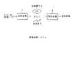
図1は、本発明を適用した画像処理システム(システムとは、複数の装置が論理的に集合したものをいい、各構成の装置が同一筐体中にあるか否かは問わない)の一実施の形態の構成を示している。送信装置1には、ディジタル化された画像データが供給されるようになされている。 FIG. 1 is a diagram of an image processing system to which the present invention is applied (a system is a logical collection of a plurality of devices, regardless of whether each configuration device is in the same housing). 1 shows a configuration of an embodiment. The
送信装置1は、入力された画像データに対して、所定の演算処理を施すことで、その画素数を間引く(少なくする)ことにより圧縮、符号化し、その結果得られる符号化データを、例えば、光ディスクや、光磁気ディスク、磁気テープ、相変化ディスクその他でなる記録媒体2に記録し、または、例えば、地上波や、衛星回線、電話回線、CATV網、インターネットその他の伝送路3を介して伝送する。 The
受信装置4では、記録媒体2に記録された符号化データが再生され、または、伝送路3を介して伝送されてくる符号化データが受信され、その符号化データが伸張、復号化される。そして、その結果得られる復号画像は、図示せぬディスプレイに供給されて表示される。 In the
なお、以上のような画像処理システムは、例えば、光ディスク装置や、光磁気ディスク装置、磁気テープ装置その他の、画像の記録/再生を行う装置や、あるいはまた、例えば、テレビ電話装置や、テレビジョン放送システム、CATVシステムその他の、画像の伝送を行う装置などに適用される。また、図1の画像処理システムは、伝送レートの低い、例えば、携帯電話機その他の、移動に便利な携帯端末などにも適用可能である。 Note that the image processing system as described above is, for example, an optical disk device, a magneto-optical disk device, a magnetic tape device, or other devices that record / reproduce images, or, for example, a videophone device or a television. The present invention is applied to a broadcasting system, a CATV system, and other devices that transmit images. The image processing system in FIG. 1 can also be applied to a mobile terminal having a low transmission rate, such as a mobile phone or the like that is convenient for movement.
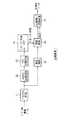
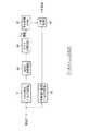
図2は、図1の送信装置1の構成例を示している。 FIG. 2 shows a configuration example of the
ブロック化回路11には、符号化すべき画像データが入力されるようになされており、ブロック化回路11は、画像データを、その性質に応じて所定のクラス(第1のクラス)に分類するための単位である、例えば、注目される画素を中心とする複数の画素で構成されるクラス分類用ブロックにブロック化し、ADRC(Adaptive Dynamic Range Coding)処理回路12および遅延回路15に供給するようになされている。 The
ADRC処理回路12は、ブロック化回路11からのブロック(クラス分類用ブロック)に対してADRC処理を施し、その結果得られるADRCコードで構成されるブロックを、クラス分類回路13に供給するようになされている。 The ADRC
ここで、ADRC処理よれば、クラス分類用ブロックを構成する画素のビット数が低減されるようになされている。 Here, according to the ADRC processing, the number of bits of the pixels constituting the class classification block is reduced.
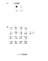
即ち、例えば、いま、説明を簡単にするため、図3(A)に示すように、直線上に並んだ4画素で構成されるブロックを考えると、ADRC処理においては、その画素値の最大値MAXと最小値MINが検出される。そして、DR=MAX−MINを、ブロックの局所的なダイナミックレンジとし、このダイナミックレンジDRに基づいて、ブロックを構成する画素の画素値がKビットに再量子化される。 That is, for example, in order to simplify the description, as shown in FIG. 3A, when a block composed of four pixels arranged on a straight line is considered, in ADRC processing, the maximum value of the pixel value is considered. MAX and minimum value MIN are detected. Then, DR = MAX−MIN is set as the local dynamic range of the block, and the pixel values of the pixels constituting the block are requantized to K bits based on the dynamic range DR.
即ち、ブロック内の各画素値から、最小値MINを減算し、その減算値をDR/2Kで除算する。そして、その結果得られる除算値に対応するコード(ADRCコード)に変換される。具体的には、例えば、K=2とした場合、図3(B)に示すように、除算値が、ダイナミックレンジDRを4(=22)等分して得られるいずれの範囲に属するかが判定され、除算値が、最も下のレベルの範囲、下から2番目のレベルの範囲、下から3番目のレベルの範囲、または最も上のレベルの範囲に属する場合には、それぞれ、例えば、00B,01B,10B、または11Bなどの2ビットにコード化される(Bは2進数であることを表す)。そして、復号側においては、ADRCコード00B,01B,10B、または11Bは、ダイナミックレンジDRを4等分して得られる最も下のレベルの範囲の中心値L00、下から2番目のレベルの範囲の中心値L01、下から3番目のレベルの範囲の中心値L10、または最も上のレベルの範囲の中心値L11にそれぞれ変換され、その値に、最小値MINが加算されることで復号が行われる。That is, from each pixel value in the block, subtracts the minimum value MIN, dividing the subtracted value by DR / 2K. Then, it is converted into a code (ADRC code) corresponding to the division value obtained as a result. Specifically, for example, when K = 2, as shown in FIG. 3B, the division value belongs to which range obtained by equally dividing the dynamic range DR by 4 (= 22 ). And the division value belongs to the range of the lowest level, the range of the second level from the bottom, the range of the third level from the bottom, or the range of the highest level, respectively, It is coded into 2 bits such as 00B, 01B, 10B, or 11B (B represents a binary number). On the decoding side, the ADRC code 00B, 01B, 10B, or 11B is the center value L00 of the lowest level range obtained by equally dividing the dynamic range DR into four, and the second level range from the bottom. center value L01 of are converted respectively to the center value L11 of the central value L10 or most of the upper level range, the range of the third level from the bottom, to the value, that the minimum value MIN is added Decryption is performed.
以上のようなADRC処理によれば、ブロックを構成する画素に割り当てられているビット数より少ないビット数で再量子化を行うことで、そのビット数を低減することができる。 According to the ADRC processing as described above, the number of bits can be reduced by performing re-quantization with the number of bits smaller than the number of bits allocated to the pixels constituting the block.
ここで、このようなADRC処理はノンエッジマッチングと呼ばれる。 Here, such ADRC processing is called non-edge matching.
なお、ADRC処理については、本件出願人が先に出願した、例えば、特開平3−53778号公報などに、その詳細が開示されている。 The details of the ADRC processing are disclosed in, for example, Japanese Patent Application Laid-Open No. 3-53778 filed by the applicant of the present application.
図2に戻り、クラス分類回路13は、ADRC処理回路12からのブロックを、その性質に応じて所定のクラスに分類するクラス分類処理を行い、そのブロックがいずれのクラスに属するかを、クラス情報として、マッピング係数メモリ14に供給するようになされている。 Returning to FIG. 2, the
ここで、クラス分類処理について説明する。いま、例えば、図4(A)に示すように、ある注目画素と、それに隣接する3つの画素により、2×2画素でなるブロック(クラス分類用ブロック)を構成し、また、各画素は、1ビットで表現される(0または1のうちのいずれかのレベルをとる)ものとする。この場合、2×2の4画素のブロックは、各画素のレベル分布により、図4(B)に示すように、16(=(21)4)パターンに分類することができる。即ち、注目画素の分類を行うことができ、このようなパターン分けが、クラス分類処理であり、クラス分類回路13において行われる。Here, the class classification process will be described. Now, for example, as shown in FIG. 4A, a pixel of interest and three adjacent pixels form a 2 × 2 pixel block (class classification block). It is expressed by 1 bit (takes a level of 0 or 1). In this case, the 2 × 2 4-pixel block can be classified into 16 (= (21 )4 ) patterns as shown in FIG. 4B, depending on the level distribution of each pixel. That is, the pixel of interest can be classified, and such pattern classification is class classification processing and is performed in the
なお、クラス分類処理は、画像(ブロック内の画像)のアクティビティ(画像の複雑さ)(変化の激しさ)(動き量)などをも考慮して行うようにすることが可能である。 The class classification process can be performed in consideration of the activity (complexity of the image) (the intensity of change) (the amount of movement) of the image (the image in the block).
ここで、符号化すべき画像データに、例えば8ビットが割り当てられている場合において、クラス分類用ブロックが、例えば3×3の9画素で構成されるときに、そのようなクラス分類用ブロックを対象にクラス分類処理を行ったのでは、(28)9という膨大な数のクラスに分類されることになる。Here, when, for example, 8 bits are allocated to the image data to be encoded, when the class classification block is composed of, for example, 9 pixels of 3 × 3, such a class classification block is targeted. If the class classification process is performed, it is classified into an enormous number of classes of (28 )9 .
そこで、上述したように、ADRC処理回路12において、クラス分類用ブロックに対して、ADRC処理が施されるようになされており、これにより、クラス分類用ブロックを構成する画素のビット数を低減し、さらに、クラス数も削減するようになされている。即ち、ADRC処理回路12において、例えば1ビットのADRC処理が行われるとした場合には、クラス数は、(28)9から(21)9、即ち、512に低減される。Therefore, as described above, the ADRC
なお、本実施の形態では、クラス分類回路13において、ADRC処理回路12から出力されるADRCコードに基づいて、クラス分類処理が行われるが、クラス分類処理は、その他、例えば、DPCM(予測符号化)や、BTC(Block Truncation Coding)、VQ(ベクトル量子化)、DCT(離散コサイン変換)、アダマール変換などを施したデータを対象に行うようにすることも可能である。 In the present embodiment, the
再び、図2に戻り、マッピング係数メモリ14は、後述するような学習(マッピング係数学習)により得られるマッピング係数を、クラス情報ごとに記憶しており、クラス分類回路13から供給されるクラス情報をアドレスとして、そのアドレスに記憶されているマッピング係数を読み出し、演算回路16に供給するようになされている。 2 again, the
遅延回路15は、ブロック化回路11から供給されるブロックを、そのブロックのクラス情報に対応するマッピング係数が、マッピング係数メモリ14から読み出されるまで遅延し、演算回路16に供給するようになされている。 The
演算回路16は、遅延回路15から供給されるブロックを構成する画素の画素値と、マッピング係数メモリ14から供給される、そのブロックのクラスに対応するマッピング係数とを用いて所定の演算を行うことにより、画像を、その画素数を間引いて(少なくして)符号化した符号化データを算出するようになされている。即ち、演算回路16は、ブロック化回路11が出力するブロックを構成する各画素の画素値をy1,y2,・・・とするとともに、マッピング係数メモリ14が出力する、そのブロックのクラスに対応するマッピング係数をk1,k2,・・・とするとき、それらを引数とする所定の関数値f(y1,y2,・・・,k1,k2,・・・)を演算し、その関数値f(y1,y2,・・・,k1,k2,・・・)を、ブロック化回路11が出力するブロック(クラス分類用ブロック)を構成する画素のうちの、例えば中心の画素の画素値として出力するようになされている。The
従って、ブロック化回路11が出力するクラス分類用ブロックを構成する画素数をNとすると、演算回路16は、画像データを1/Nに間引き、これを、符号化データとして出力するようになされている。 Therefore, if the number of pixels constituting the class classification block output by the
なお、演算回路16が出力する符号化データは、N画素で構成されるブロックの中心の画素を抽出して出力するような、いわば単純な間引き処理により得られるものではなく、上述したように、そのブロックを構成するN画素により規定される関数値f(y1,y2,・・・,k1,k2,・・・)であるが、この関数値f(y1,y2,・・・,k1,k2,・・・)は、見方を変えれば、単純な間引き処理により得られる、ブロックの中心の画素の画素値を、その周辺の画素値に基づいて補正したものと考えることができる。そこで、マッピング係数と、ブロックを構成する画素との演算の結果得られるデータである符号化データを、以下、適宜、補正データともいう。It should be noted that the encoded data output from the
また、演算回路16における演算処理は、ブロック化回路11が出力するクラス分類用ブロックを構成する各画素の画素値を、関数値f(y1,y2,・・・,k1,k2,・・・)にマッピング(写像)する処理とも考えることができる。そこで、そのような処理に用いられる係数k1,k2,・・・をマッピング係数と呼んでいる。Further, the arithmetic processing in the
送信機/記録装置17は、演算回路16から符号化データとして供給される補正データを、記録媒体2に記録し、または伝送路3を介して伝送するようになされている。 The transmitter /
次に、図5のフローチャートを参照して、その動作について説明する。 Next, the operation will be described with reference to the flowchart of FIG.
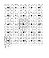
ブロック化回路11には、例えば、1フレーム単位で画像データが供給されるようになされており、ブロック化回路11では、ステップS1において、1フレームの画像が、クラス分類用ブロックにブロック化される。即ち、ブロック化回路11は、例えば、図6に四角形で囲んで示すように、画像データを、注目画素(図6の実施の形態では、同図に●印で示す横および縦に2個おきの画素が注目画素になり得る)を中心とした3×3(横×縦)の9画素でなるクラス分類用ブロックに分割し、ADRC処理回路12および遅延回路15に、順次供給する。 For example, image data is supplied to the
なお、この場合、クラス分類用ブロックは、3×3画素でなる正方形状のブロックで構成されることとなるが、クラス分類用ブロックの形状は、正方形である必要はなく、その他、例えば、長方形や、十文字形、その他の任意な形とすることが可能である。また、クラス分類用ブロックを構成する画素数も、3×3の9画素に限定されるものではない。さらに、クラス分類用ブロックは、隣接する画素どうしで構成するのではなく、離れた画素どうしで構成するようにすることも可能である。但し、その形状および画素数は、後述する学習(マッピング係数学習)時における場合のものと一致している必要がある。 In this case, the class classification block is configured by a square block of 3 × 3 pixels. However, the shape of the class classification block does not have to be a square, for example, a rectangle Or a cross-shaped or any other shape. Further, the number of pixels constituting the class classification block is not limited to 3 × 3 9 pixels. Furthermore, the class classification block may be configured not with adjacent pixels but with distant pixels. However, the shape and the number of pixels need to match those in the case of learning (mapping coefficient learning) described later.
ADRC処理回路12は、ブロック化回路11からクラス分類用ブロックを受信すると、ステップS2において、そのブロックに対して、例えば、1ビットのADRC処理を施し、これにより、1ビットで表現される画素で構成されるブロックとする。ADRC処理の施されたクラス分類用ブロックは、クラス分類回路13に供給される。 When the
クラス分類回路13では、ステップS3において、ADRC処理回路12からのクラス分類用ブロックがクラス分類され、その結果得られるクラス情報が、マッピング係数メモリ14に、アドレスとして供給される。これにより、マッピング係数メモリ14からは、クラス分類回路13より供給されたクラス情報に対応するマッピング係数が読み出され、演算回路16に供給される。 In step S3, the
一方、遅延回路15では、ブロック化回路11からのクラス分類用ブロックが遅延され、そのブロックのクラス情報に対応するマッピング係数が、マッピング係数メモリ14から読み出されるのを待って、演算器16に供給される。演算器16では、ステップS4において、遅延回路15からのクラス分類用ブロックを構成する各画素の画素値と、マッピング係数メモリ14からのマッピング係数を用いて、上述した関数値f(・)(この関数fのかっこ内の・は、画素値y1,y2,・・・と、マッピング係数k1,k2,・・・の集合を表すものとする)が演算されることにより、クラス分類用ブロックを構成する中心の画素(中心画素)の画素値を補正した補正データが算出される。この補正データは、画像を符号化した符号化データとして、送信機/記録装置17に供給される。On the other hand, in the
送信機/記録装置17では、ステップS5において、演算回路16からの符号化データが、記録媒体2に記録され、または伝送路3を介して伝送される。 In the transmitter /
そして、ステップS6に進み、1フレーム分の画像データについての処理が終了したかどうかが判定される。ステップS6において、1フレーム分の画像データについての処理が、まだ終了していないと判定された場合、ステップS2に戻り、次のクラス分類用ブロックを対象に、ステップS2以下の処理が繰り返される。また、ステップS6において、1フレーム分の画像データについての処理が終了したと判定された場合、ステップS1に戻り、次のフレームを対象に、ステップS1以下の処理が繰り返される。 In step S6, it is determined whether or not the processing for one frame of image data has been completed. If it is determined in step S6 that the processing for the image data for one frame has not been completed yet, the process returns to step S2, and the processes in and after step S2 are repeated for the next class classification block. If it is determined in step S6 that the processing for the image data for one frame has been completed, the process returns to step S1, and the processing in step S1 and subsequent steps is repeated for the next frame.
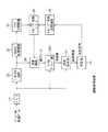
次に、図7は、図2のマッピング係数メモリ14に記憶されているマッピング係数を算出するための学習(マッピング係数学習)処理を行う画像処理装置の第1の構成例を示している。 Next, FIG. 7 shows a first configuration example of an image processing apparatus that performs learning (mapping coefficient learning) processing for calculating the mapping coefficient stored in the
メモリ21には、学習に適したディジタル画像データ(以下、適宜、学習用画像という)が1フレーム以上記憶されている。ブロック化回路22は、メモリ21に記憶されている画像データを読み出し、図2のブロック化回路11から出力されるクラス分類用ブロックと同一のブロックを構成して、ADRC処理回路23および演算回路26に供給するようになされている。 The
ADRC処理回路23またはクラス分類回路24は、図2のADRC処理回路12またはクラス分類回路13における場合とそれぞれ同様の処理を行うようになされている。従って、クラス分類回路24からは、ブロック化回路22が出力するブロックのクラス情報が出力されるようになされている。そして、このクラス情報は、マッピング係数メモリ31に、アドレスとして供給されるようになされている。 The
演算器26は、ブロック化回路22から供給されるブロックを構成する画素と、マッピング係数メモリ31から供給されるマッピング係数とを用いて、図2の演算回路16における場合と同一の演算を行い、その結果得られる補正データ(関数値f(・))を、ローカルデコード部27に供給するようになされている。 The
ローカルデコード部27は、演算回路26から供給される補正データに基づいて、元の学習用画像の予測値(ブロック化回路22が出力するブロックを構成する画素の画素値の予測値)を予測し(算出し)、誤差算出部28に供給するようになされている。誤差算出部28は、ローカルデコード部27から供給される予測値に対応する学習用画像の画素値(真値)をメモリ21から読み出し、その学習用画像の画素値に対する、予測値の予測誤差を算出(検出)し、その予測誤差を、誤差情報として、判定部29に供給するようになされている。 Based on the correction data supplied from the
判定部29は、誤差算出部28からの誤差情報と、所定の閾値ε1とを比較し、その比較結果に対応して、マッピング係数設定回路30を制御するようになされている。マッピング係数設定回路30は、判定部29の制御にしたがって、クラス分類回路24におけるクラス分類の結果得られるクラス数と同一の数のマッピング係数のセットを設定(変更)し、マッピング係数メモリ31に供給するようになされている。 The
マッピング係数メモリ31は、マッピング係数設定回路30から供給されるマッピング係数を一時記憶するようになされている。なお、マッピング係数メモリ31は、クラス分類回路24においてクラス分類されるクラスの数だけのマッピング係数(マッピング係数のセット)を記憶することのできる記憶領域を有しており、各記憶領域においては、マッピング係数設定回路30から、新たなマッピング係数が供給されると、既に記憶しているマッピング係数に代えて、その新たなマッピング係数が記憶されるようになされている。 The mapping coefficient memory 31 is configured to temporarily store the mapping coefficient supplied from the mapping
また、マッピング係数メモリ31は、クラス分類回路24から供給されるクラス情報に対応するアドレスに記憶されたマッピング係数を読み出し、演算回路26に供給するようにもなされている。 Further, the mapping coefficient memory 31 reads out the mapping coefficient stored at the address corresponding to the class information supplied from the
次に、図8のフローチャートを参照して、その動作について説明する。 Next, the operation will be described with reference to the flowchart of FIG.
まず最初に、マッピング係数設定回路30は、ステップS51においてマッピング係数の初期値のセットを、クラス分類回路24においてクラス分類されるクラスの数だけ設定し、マッピング係数メモリ31に供給する。マッピング係数メモリ31では、マッピング係数設定回路30からのマッピング係数(初期値)が、対応するクラスのアドレスに記憶される。 First, the mapping
そして、ブロック化回路22は、ステップS52において、メモリ21に記憶されている学習用画像すべてを、図2のブロック化回路11における場合と同様に、注目画素を中心に3×3画素のブロックにブロック化する。さらに、ブロック化回路21は、そのブロックを、メモリ21から読み出し、ADRC処理回路23および演算回路26に順次供給する。 Then, in step S52, the blocking
ADRC処理回路23では、ステップS53において、ブロック化回路22からのブロックに対して、図2のADRC処理回路12における場合と同様に、1ビットのADRC処理が施され、クラス分類回路24に供給される。クラス分類回路24では、ステップS54において、ADRC処理回路23から供給されたブロックのクラスが決定され、そのクラス情報が、アドレスとして、マッピング係数メモリ31に供給される。これにより、ステップS55において、マッピング係数メモリ31の、クラス分類回路24から供給されるクラス情報に対応するアドレスから、マッピング係数が読み出され、演算回路26に供給される。 In the
演算回路26は、ブロック化回路22からブロックを受信するとともに、マッピング係数メモリ31から、そのブロックのクラスに対応するマッピング係数を受信すると、ステップS56において、そのマッピング係数と、ブロック化回路22から供給されるブロックを構成する画素の画素値とを用いて、上述の関数値f(・)を演算する。この演算結果は、ブロック化回路22から供給されるブロックの中心画素の画素値を補正した補正データとして、ローカルデコード部27に供給される。 When the
即ち、例えば、上述の図6において、四角形で囲んで示すような3×3画素のブロックが、ブロック化回路22から出力されたものとすると、演算回路26では、同図において●印で示す画素の画素値を補正した補正データが求められ、ローカルデコード部27に出力される。 That is, for example, in FIG. 6, assuming that a block of 3 × 3 pixels as enclosed by a rectangle is output from the blocking
従って、演算回路26では、学習用画像を構成する画素数が、1/9に間引かれ、ローカルデコード部27に供給される。 Therefore, in the
ここで、図6において、上からi番目で、左からj番目の●印で示す画素に対応する補正データをXijと表すととともに、その補正データXijを中心とする、元の学習用画像(原画像)における3×3の9画素の画素値を、その最も左から右方向、かつ上から下方向に、Yij(1),Yij(2),Yij(3),Yij(4),Yij(5),Yij(6),Yij(7),Yij(8),Yij(9)と表すこととする。Here, in FIG. 6, the i-th from the top, the correction data corresponding to pixels indicated by the j-th mark ● left with expressed as Xij, centered on the correction data Xij, for the original training The pixel values of 3 × 3 9 pixels in the image (original image) areconverted into Yij (1), Yij (2), Yij (3), Y from the leftmost to the right and from the top to the bottom.ij (4), Yij (5), Yij (6), Yij (7), Yij (8), Yij (9).
図8に戻り、ステップS56で補正データが算出された後は、ステップS57に進み、メモリ21に記憶されたすべての学習用画像についての補正データが求められたかどうかが判定される。ステップS57において、すべての学習用画像についての補正データが、まだ求められていないと判定された場合、ステップS53に戻り、すべての学習用画像についての補正データが求められるまで、ステップS53乃至S57の処理を繰り返す。 Returning to FIG. 8, after the correction data is calculated in step S <b> 56, the process proceeds to step S <b> 57 and it is determined whether correction data for all the learning images stored in the
また、ステップS57において、すべての学習用画像についての補正データが求められたと判定された場合、即ち、メモリ21に記憶されたすべての学習用画像を、1/9に間引いた間引き画像が得られた場合(但し、この間引き画像は、学習用画像を、単純に1/9に間引いたものではなく、マッピング係数との演算により画素値が求められたものである)、ステップS58に進み、ローカルデコード部27において、その間引き画像がローカルデコードされることにより、元の学習用画像の予測値が算出される。この予測値は、誤差算出部28に供給される。 If it is determined in step S57 that correction data for all learning images has been obtained, that is, a thinned image obtained by thinning all the learning images stored in the
ここで、このローカルデコード部27において得られる予測値で構成される画像(但し、後述するように、誤差情報算出部28から出力される誤差情報が閾値ε1より小さくなったときにおけるもの)は、受信装置4(図1)側において得られる復号画像と同一のものである。 Here, an image composed of predicted values obtained by the local decoding unit 27 (however, as described later, when the error information output from the error
誤差算出部28では、ステップS59において、メモリ21から学習用画像が読み出され、その学習用画像に対する、ローカルデコード部27から供給される予測値の予測誤差が算出される。即ち、学習用画像の画素値をYijと表すとともに、ローカルデコード部27から出力される、その予測値をE[Yij]と表すとき、誤差算出部28では、次式で示される誤差分散(誤差の自乗和)Qが算出され、これが、誤差情報として、判定部29に供給される。In step S59, the
Q=Σ(Yij−E[Yij])2
但し、上式において、Σは、学習用画像の画素すべてについてのサメーションを表す。Q = Σ (Yij −E [Yij ])2
However, in the above equation, Σ represents summation for all the pixels of the learning image.
判定部29は、誤差算出部28から誤差情報を受信すると、その誤差情報と所定の閾値ε1とを比較し、ステップS60において、その大小関係を判定する。ステップS60において、誤差情報が閾値ε1以上であると判定された場合、即ち、ローカルデコード部27において得られる予測値で構成される画像が、元の学習用画像と同一であるとは認められない場合、判定部29は、マッピング係数設定回路30に制御信号を出力する。マッピング係数設定回路30は、ステップS61において、判定部29からの制御信号にしたがい、マッピング係数を変更し、その変更後のマッピング係数を、マッピング係数メモリ31に新たに記憶させる。 When receiving the error information from the
そして、ステップS53に戻り、マッピング係数メモリ31に記憶された、変更後のマッピング係数を用いて、再び、ステップS53以下の処理が繰り返される。 Then, the process returns to step S53, and the process after step S53 is repeated again using the changed mapping coefficient stored in the mapping coefficient memory 31.
ここで、マッピング係数設定回路30における、マッピング係数の変更は、ランダムに行っても良いし、また、今回の誤差情報が、前回の誤差情報より小さくなった場合には、前回と同様の傾向で変化させ、今回の誤差情報が、前回の誤差情報より大きくなった場合には、前回と逆の傾向で変化させるようにすることもできる。 Here, the mapping coefficient in the mapping
さらに、マッピング係数の変更は、すべてのクラスについて行うようにすることもできるし、その一部のクラスについてだけ行うようにすることもできる。一部のクラスについてのマッピング係数だけの変更を行う場合においては、例えば、誤差情報に対する影響の強いクラスを検出させ、そのようなクラスについてのマッピング係数だけを変更するようにすることができる。誤差情報に対する影響の強いクラスは、例えば、次のようにして検出することができる。即ち、まず最初に、マッピング係数の初期値を用いて処理を行うことにより、その誤差情報を得る。そして、マッピング係数を、1クラスごとに同一の量だけ変化させ、その結果得られる誤差情報を、初期値を用いた場合に得られた誤差情報と比較し、その差が、所定値以上となるクラスを、誤差情報に対する影響の強いクラスとして検出すれば良い。 Further, the mapping coefficient can be changed for all classes or only for some of the classes. In the case of changing only the mapping coefficients for some classes, for example, a class having a strong influence on error information can be detected, and only the mapping coefficients for such classes can be changed. The class having a strong influence on the error information can be detected as follows, for example. That is, first, the error information is obtained by performing processing using the initial value of the mapping coefficient. Then, the mapping coefficient is changed by the same amount for each class, and the error information obtained as a result is compared with the error information obtained when the initial value is used, and the difference becomes a predetermined value or more. The class may be detected as a class having a strong influence on the error information.
また、マッピング係数が、上述したk1,k2,・・・のように複数で1セットとされている場合には、その中の誤差情報に対する影響の強いものだけを変更させるようにすることもできる。 In addition, when there are a plurality of mapping coefficients such as k1, k2,... Described above, only the one having a strong influence on the error information can be changed. .
さらに、上述の場合においては、マッピング係数を、クラスごとに設定するようにしたが、マッピング係数は、その他、例えば、ブロックごとに独立して設定したり、また、近接するブロック単位などで設定したりするようにすることが可能である。 Furthermore, in the above-described case, the mapping coefficient is set for each class. However, the mapping coefficient is set separately for each block, for example, or in units of adjacent blocks. It is possible to make it.
但し、マッピング係数を、例えば、ブロックごとに独立して設定するようにした場合などにおいては、ある1つのクラスに対して、複数セットのマッピング係数が得られることがある(この逆に、マッピング係数が、1セットも得られないクラスが生じることもある)。マッピング係数は、最終的には、クラスごとに決める必要があるため、上述のように、あるクラスに対して、複数セットのマッピング係数が得られた場合には、複数セットのマッピング係数を対象に、何らかの処理を行うことで、1セットのマッピング係数を決める必要がある。 However, when mapping coefficients are set independently for each block, for example, multiple sets of mapping coefficients may be obtained for a certain class (conversely, mapping coefficients). However, there may be classes that cannot be obtained in one set). Since the mapping coefficients need to be finally determined for each class, as described above, when multiple sets of mapping coefficients are obtained for a certain class, multiple sets of mapping coefficients are targeted. It is necessary to determine one set of mapping coefficients by performing some processing.
一方、ステップS60において、誤差情報が閾値ε1より小さいと判定された場合、即ち、ローカルデコード部27において得られる予測値で構成される画像が、元の学習用画像と同一であると認められる場合、処理を終了する。 On the other hand, when it is determined in step S60 that the error information is smaller than the threshold ε1, that is, when the image composed of the prediction values obtained in the
この時点で、マッピング係数メモリ31に記憶されている、クラスごとのマッピング係数が、もとの画像と同一と認められる復号画像(予測値)を復元することができる補正データを得るために最適なものとして、図2のマッピング係数メモリ14にセットされている。 At this time, it is optimum to obtain correction data that can restore a decoded image (predicted value) in which the mapping coefficient for each class stored in the mapping coefficient memory 31 is recognized to be the same as the original image. As a thing, it is set in the
従って、このようなマッピング係数を用いて補正データを生成することで、受信装置4(図1)側においては、元の画像とほぼ同一の画像を得ることが可能となる。 Therefore, by generating correction data using such a mapping coefficient, it is possible to obtain an image that is substantially the same as the original image on the receiving device 4 (FIG. 1) side.
なお、図7の実施の形態においては、上述したように、ブロック化回路22において、画像が、注目画素を中心として3×3の9画素にブロック化され、また、ADRC処理回路23において、1ビットのADRC処理が行われるので、クラス分類回路24によるクラス分類により得られるクラス数は512(=(21)9)であり、従って、512セットのマッピング係数が得られる。In the embodiment of FIG. 7, as described above, in the blocking
次に、図9は、図7のローカルデコード部27の構成例を示している。 Next, FIG. 9 shows a configuration example of the
演算回路26からの補正データは、クラス分類用ブロック化回路41および予測値計算用ブロック化回路42に供給されるようになされている。クラス分類用ブロック化回路41は、補正データを、その性質に応じて所定のクラスに分類するための単位である、注目補正データを中心としたクラス分類用ブロックにブロック化するようになされている。 The correction data from the
即ち、上述したように、図6において、上からi番目で、左からj番目の補正データ(圧縮データ)(画素)(図中、●印で示す部分)をXijと表すとすると、クラス分類用ブロック化回路41は、例えば、注目補正データXijの左上、上、右上、左、右、左下、下、右下に隣接する8つの補正データX(i-1)(j-1),X(i-1)j,X(i-1)(j+1),Xi(j-1),Xi(j+1),X(i-1)(j-1),X(i-1)j,X(i+1)(j+1)に、自身を含め、合計9画素で構成されるクラス分類用ブロックを生成するようになされている。このクラス分類用ブロックは、ADRC処理回路43に供給されるようになされている。That is, as described above, in FIG. 6, if the i-th correction data (compressed data) (pixel) (pixel) in the figure from the top and the j-th from the left is represented as Xij , the class
なお、図9のクラス分類用ブロック化回路41において得られるクラス分類用ブロックは、予測値を求めるブロックのクラス(第2のクラス)を決定するために構成されるものであり、この点で、補正データを算出するブロックのクラス(第1のクラス)を決定するために、図2のブロック化回路11で生成されるものとは異なる。 Note that the class classification block obtained in the class
予測値計算用ブロック化回路42は、補正データを、元の画像(ここでは、学習用画像)の予測値を計算するための単位である、注目補正データを中心とした予測値計算用ブロックにブロック化するようになされている。即ち、本実施の形態においては、例えば、補正データXijを中心とする、元の画像(原画像)における3×3の9画素の画素値Yij(1),Yij(2),Yij(3),Yij(4),Yij(5),Yij(6),Yij(7),Yij(8),Yij(9)の予測値が、画素Xijを中心とする5×5の25画素X(i-2)(j-2),X(i-2)(j-1),X(i-2)j,X(i-2)(j+1),X(i-2)(j+2),X(i-1)(j-2),X(i-1)(j-1),X(i-1)j,X(i-1)(j+1),X(i-1)(j+2),Xi(j-2),Xi(j-1),Xij,Xi(j+1),Xi(j+2),X(i+1)(j-2),X(i+1)(j-1),X(i+1)j,X(i+1)(j+1),X(i+1)(j+2),X(i+2)(j-2),X(i+2)(j-1),X(i+2)j,X(i+2)(j+1),X(i+2)(j+2)から求められるようになされており、予測値計算用ブロック化回路42は、このような25画素で構成される正方形状の予測値計算用ブロックを生成するようになされている。The predicted value
具体的には、例えば、図6において四角形で囲む、元の画像における画素Y33(1)乃至Y33(9)の予測値の計算のためには、25の画素(補正データ)X11,X12,X13,X14,X15,X21,X22,X23,X24,X25,X31,X32,X33,X34,X35,X41,X42,X43,X44,X45,X51,X52,X53,X54,X55により、予測値計算用ブロックが構成される。Specifically, for example, in order to calculate predicted values of pixels Y33 (1) to Y33 (9) in the original image enclosed by a rectangle in FIG. 6, 25 pixels (correction data) X11 ,X 12, X 13, X 14 ,
予測値計算用ブロック化回路42において得られた予測値計算用ブロックは、予測回路46に供給されるようになされている。 The prediction value calculation block obtained in the prediction value calculation
なお、予測値計算用ブロックについても、クラス分類用ブロックにおける場合と同様に、その画素数および形状は、上述したものに限定されるものではない。但し、ローカルデコード部27において、予測値計算用ブロックを構成する画素数は、クラス分類用ブロックを構成する画素数よりも多くするのが望ましい。 Note that the number of pixels and the shape of the prediction value calculation block are not limited to those described above, as in the case of the class classification block. However, in the
また、上述のようなブロック化を行う場合において(ブロック化以外の処理についても同様)、画像の画枠付近では、対応する画素が存在しないことがあるが、この場合には、例えば、画枠を構成する画素と同一の画素が、その外側に存在するものとして処理を行う。 Further, when the above-described blocking is performed (the same applies to processes other than blocking), there may be no corresponding pixel near the image frame of the image. In this case, for example, the image frame The processing is performed on the assumption that the same pixel as that constituting the pixel exists outside.
ADRC処理回路43は、クラス分類用ブロック化回路41が出力するブロック(クラス分類用ブロック)に対して、例えば、1ビットのADRC処理を施し、クラス分類回路44に供給するようになされている。クラス分類回路44は、ADRC処理回路43からのブロックをクラス分類し、その分類結果としてのクラス情報を、予測係数ROM45に供給するようになされている。予測係数ROM45は、クラスごとの予測係数を記憶しており、クラス分類回路44からクラス情報を受信すると、そのクラス情報に対応するアドレスに記憶されている予測係数を読み出し、予測回路46に供給するようになされている。なお、予測係数ROM45に記憶されているクラスごとの予測係数は、後述する学習(予測係数学習)により得られたものである。 The
予測回路46は、予測値計算用ブロック化回路42からの予測値計算用ブロックと、予測係数ROM45からの予測係数とを用いて、元の画像(学習用画像)の予測値を算出(予測)するようになされている。 The
次に、図10のフローチャートを参照して、その動作について説明する。 Next, the operation will be described with reference to the flowchart of FIG.
ローカルデコード部27においては、まず最初に、ステップS21において、演算回路26からの補正データが順次受信されてブロック化される。即ち、クラス分類用ブロック化回路41において、補正データが、注目補正データを中心とする3×3画素のクラス分類用ブロックにブロック化され、ADRC処理回路43に供給されるとともに、予測値計算用ブロック化回路42において、補正データが、注目補正データを中心とする5×5画素の予測値計算用ブロックにブロック化され、予測回路46に供給される。 In the
なお、クラス分類用ブロック化回路41と予測値計算用ブロック化回路42では、対応するクラス分類用ブロックと予測値計算用ブロックが生成される。即ち、クラス分類用ブロック化回路41において、例えば図6の補正データX33を中心とする3×3画素のクラス分類用ブロックが生成されるとき、予測値計算用ブロックにおいては、同じく補正データX33を中心とする5×5画素の予測値計算用ブロックが生成される(補正データX33を注目補正データとしてクラス分類用ブロックが構成されるとき、予測値計算用ブロックも、補正データX33を注目補正データとして構成される)。The class
ADRC処理回路43は、クラス分類用ブロックを受信すると、ステップS22において、そのクラス分類用ブロックに対して、例えば、1ビットのADRC(1ビットで再量子化を行うADRC)処理を施し、これにより、クラス分類用ブロックを構成する補正データを、1ビットに変換(符号化)して、クラス分類回路44に出力する。クラス分類回路44は、ステップS23において、ADRC処理が施されたクラス分類用ブロックに対して、クラス分類処理を施す。即ち、クラス分類用ブロックを構成する各画素のレベル分布の状態を検出し、そのクラス分類用ブロックが属するクラス(そのクラス分類用ブロックを構成する注目画素(注目補正データ)のクラス)を判定する。このクラスの判定結果は、クラス情報として、予測係数ROM45に供給される。 Upon receiving the class classification block, the
なお、図10の実施の形態においては、1ビットのADRC処理が施された3×3の9画素で構成されるクラス分類用ブロックに対して、クラス分類処理が施されるので、各クラス分類用ブロックは、512(=(21)9)のクラスのうちのいずれかに分類されることになる。In the embodiment of FIG. 10, class classification processing is performed on a class classification block composed of 9 pixels of 3 × 3 subjected to 1-bit ADRC processing. The block for use is classified intoone of 512 (= (21 )9 ) classes.
そして、ステップS24に進み、予測係数ROM45の、クラス分類回路44からのクラス情報に対応するアドレスから予測係数が読み出され、ステップS25において、予測回路46は、その予測係数と、予測値計算用ブロック化回路42からの予測値計算用ブロックを構成する25の画素値とを用い、例えば、次のような線形1次式にしたがって、元の画像の画素値yの予測値E[y]を算出する。 In step S24, the prediction coefficient is read from the address of the
E[y]=w1x1+w2x2+・・・
但し、w1,w2,・・・は予測係数を表し、x1,x2,・・・は予測値計算用ブロックを構成する画素の画素値(補正データ)を表す。E [y] = w1 x1 + w2 x2 +...
However, w1, w2, ··· represents a prediction coefficient, x1, x2, ··· represent the pixel values of the pixels constituting the predicted values calculation block (correction data).
ここで、図9の実施の形態においては、上述したように、予測値計算用ブロックを構成する25画素から、9画素の予測値が算出されるようになされている。 Here, in the embodiment of FIG. 9, as described above, the predicted value of 9 pixels is calculated from the 25 pixels constituting the predicted value calculation block.
即ち、例えば、いま、図6に示した補正データX33を中心とする3×3の補正データX22乃至X24,X32乃至X34,X42乃至X44でなるクラス分類用ブロックについてのクラス情報Cが、クラス分類回路44から出力され、また、予測値計算用ブロックとして、補正データX33を中心とする5×5画素の補正データX11乃至X15,X21乃至X25,X31乃至,X35,X41乃至X45,X51乃至X55でなる予測値計算用ブロックが、予測値計算用ブロック化回路42から出力されたものとする。That is, for example, the class classification block including 3 × 3 correction data X22 to X24 , X32 to X34 , and X42 to X44 centering on the correction data X33 shown in FIG. Class information C is output from the
さらに、予測係数ROM45には、クラス情報Cに対応するアドレスに、予測係数のセットとして、w1(k)乃至w25(k)が記憶されているものとする。Furthermore, it is assumed that w1 (k) to w25 (k) are stored in the
この場合、補正データX33を中心とする、元の画像における3×3画素(図6において四角形で囲んである部分)の画素値Y33(1)乃至Y33(9)の予測値E[Y33(1)]乃至E[Y33(9)]は、次式にしたがって算出される。In this case, the predicted value E [3] of pixel values Y33 (1) to Y33 (9) of 3 × 3 pixels (portion surrounded by a rectangle in FIG. 6) in the original image with the correction data X33 as the center. Y33 (1)] to E [Y33 (9)] are calculated according to the following equations.
E[Y33(k)]=w1(k)X11+w2(k)X12+w3(k)X13
+w4(k)X14+w5(k)X15+w6(k)X21
+w7(k)X22+w8(k)X23+w9(k)X24
+w10(k)X25+w11(k)X31
+w12(k)X32+w13(k)X33
+w14(k)X34+w15(k)X35
+w16(k)X41+w17(k)X42
+w18(k)X43+w19(k)X44
+w20(k)X45+w21(k)X51
+w22(k)X52+w23(k)X53
+w24(k)X54+w25(k)X55E [Y33 (k)] = w1 (k) X11 + w2 (k) X12 + w3 (k) X13
+ W4 (k) X14 + w5 (k) X15 + w6 (k) X21
+ W7 (k) X22 + w8 (k) X23 + w9 (k) X24
+ W10 (k) X25 + w11 (k) X31
+ W12 (k) X32 + w13 (k) X33
+ W14 (k) X34 + w15 (k) X35
+ W16 (k) X41 + w17 (k) X42
+ W18 (k) X43 + w19 (k) X44
+ W20 (k) X45 + w21 (k) X51
+ W22 (k) X52 + w23 (k) X53
+ W24 (k) X54 + w25 (k) X55
ステップS25において、以上のようにして予測値が、9個単位で、例えば1フレーム分だけ求められると、ステップS26に進み、その1フレーム分の予測値が、誤差算出部28に供給される。そして、次の補正データが供給されるのを待って、ステップS21に戻り、以下、ステップS21乃至S26の処理が繰り返される。 In step S25, when predicted values are obtained in units of nine, for example, for one frame as described above, the process proceeds to step S26, and the predicted value for one frame is supplied to the
次に、図11は、図9の予測係数ROM45に記憶されている予測係数を得るための学習(予測係数学習)を行う画像処理装置の構成例を示している。 Next, FIG. 11 shows a configuration example of an image processing apparatus that performs learning (prediction coefficient learning) for obtaining a prediction coefficient stored in the
学習用ブロック化回路51および教師用ブロック化回路52には、あらゆる画像に適用可能な予測係数を得るための学習用の画像データ(学習用画像)が供給されるようになされている。 The
学習用ブロック化回路51は、入力される画像データから、注目画素を中心とした、図6に●印で示した位置関係の25画素(5×5画素)を抽出し、この25画素で構成されるブロックを、学習用ブロックとして、ADRC処理53および学習データメモリ56に供給する。 The learning
また、教師用ブロック化回路52では、入力される画像データから、例えば、注目画素を中心として3×3の9画素で構成されるブロックが生成され、教師用ブロックとして、教師データメモリ58に供給される。 Also, the teacher
なお、学習用ブロック化回路51において、例えば、図6に●印で示した位置関係の25画素で構成される学習用ブロックが生成されるとき、教師用ブロック化回路52では、周囲を四角形で囲んで示す3×3画素の教師用ブロックが生成されるようになされている。 In the learning
ADRC処理回路53は、学習用ブロックを構成する25画素から、その中心の9画素(3×3画素)を抽出し、これにより、図9のクラス分類用ブロック化回路41が出力するクラス分類用ブロックと同一のブロックを構成する。さらに、ADRC処理回路53は、その9画素でなるブロックに対して、図9のADRC処理回路43における場合と同様に、1ビットのADRC処理を施す。ADRC処理の施された、3×3画素のブロックは、クラス分類回路54に供給される。クラス分類回路54では、図9のクラス分類回路44における場合と同様にして、ADRC処理回路53からのブロックがクラス分類処理され、それにより得られるクラス情報が、スイッチ55の端子aを介して、学習データメモリ56および教師データメモリ58に供給される。 The
学習データメモリ56または教師データメモリ58では、そこに供給されるクラス情報に対応するアドレスに、学習用ブロック化回路51からの学習用ブロックまたは教師用ブロック化回路52からの教師用ブロックが、それぞれ記憶される。 In the learning
従って、学習データメモリ56において、例えば、図6に●印で示した5×5画素でなるブロックが学習用ブロックとして、あるアドレスに記憶されたとすると、教師データメモリ58においては、そのアドレスと同一のアドレスに、同図において、四角形で囲んで示す3×3画素のブロックが、教師用ブロックとして記憶される。 Accordingly, in the learning
以下、同様の処理が、あらかじめ用意されたすべての学習用の画像について繰り返され、これにより、学習用ブロックと、図9のローカルデコード部27において、その学習用ブロックを構成する25画素と同一の位置関係を有する補正データで構成される予測値計算用ブロックを用いて予測値が求められる9画素で構成される教師用ブロックとが、学習用データメモリ56と、教師用データメモリ58とにおいて、同一のアドレスに記憶される。 Thereafter, the same processing is repeated for all learning images prepared in advance, whereby the learning block and the
なお、学習用データメモリ56と教師用データメモリ58においては、同一アドレスに複数の情報を記憶することができるようになされており、これにより、同一アドレスには、複数の学習用ブロックと教師用ブロックのセットを記憶することができるようになされている。 Note that the learning
その後、端子aを選択していたスイッチ55が、端子bに切り替わり、これにより、カウンタ57の出力が、アドレスとして、学習データメモリ56および教師データメモリ58に供給される。カウンタ57は、所定のクロックをカウントし、そのカウント値を出力しており、学習データメモリ56または教師データメモリ58では、そのカウント値に対応するアドレスに記憶された学習用ブロックまたは教師用ブロックがそれぞれ読み出され、演算回路59に供給される。 Thereafter, the
従って、演算回路59には、カウンタ57のカウント値に対応するクラスの学習用ブロックのセットと、教師用ブロックのセットとが供給される。 Accordingly, the
演算回路59は、あるクラスについての学習用ブロックのセットと、教師用ブロックのセットとを受信すると、それらを用いて、最小自乗法により、誤差を最小とする予測係数を算出する。 When the
即ち、例えば、いま、学習用ブロックを構成する画素の画素値を、x1,x2,x3,・・・とし、求めるべき予測係数をw1,w2,w3,・・・とするとき、これらの線形1次結合により、教師用ブロックを構成する、ある画素の画素値yを求めるには、予測係数w1,w2,w3,・・・は、次式を満たす必要がある。That is, for example, the pixel values of the pixels constituting the learning block are now x1 , x2 , x3 ,... And the prediction coefficients to be obtained are w1 , w2 , w3 ,. Then, in order to obtain the pixel value y of a certain pixel constituting the teacher block by these linear linear combinations, the prediction coefficients w1 , w2 , w3 ,... There is.
y=w1x1+w2x2+w3x3+・・・y = w1 x1 + w2 x2 + w3 x3 +...
そこで、演算回路59では、同一クラスの学習用ブロックと、対応する教師用ブロックとから、真値yに対する、予測値w1x1+w2x2+w3x3+・・・の自乗誤差を最小とする予測係数w1,w2,w3,・・・が求められる。Therefore, the
以上の処理がクラスごとに行われ、各クラスごとに、25×9の予測係数が求められる。 The above processing is performed for each class, and a 25 × 9 prediction coefficient is obtained for each class.
ここで、演算回路59の処理について、さらに説明する。 Here, the processing of the
例えば、いま、元の画像の画素値yの予測値E[y]を、その周辺の幾つかの画素の画素値(以下、適宜、学習データという)x1,x2,・・・と、所定の予測係数w1,w2,・・・の線形結合により規定される線形1次結合モデルにより求めることを考えると、予測値E[y]は、次式で表すことができる。For example, now, the predicted value E [y] of the pixel value y of the original image is changed to pixel values (hereinafter referred to as learning data) x1 , x2 ,. In consideration of obtaining by a linear linear combination model defined by linear combination of predetermined prediction coefficients w1 , w2 ,..., The predicted value E [y] can be expressed by the following equation.
E[y]=w1x1+w2x2+・・・
・・・(1)E [y] = w1 x1 + w2 x2 +...
... (1)
そこで、予測係数wの集合でなる行列W、学習データxの集合でなる行列X、および予測値E[y]の集合でなる行列Y’を、
XW=Y’
・・・(2)XW = Y '
... (2)
そして、この観測方程式に最小自乗法を適用して、元の画像の画素値yに近い予測値E[y]を求めることを考える。この場合、元の画像の画素値(以下、適宜、教師データという)yの集合でなる行列Y、および元の画像の画素値yに対する予測値E[y]の残差eの集合でなる行列Eを、
XW=Y+E
・・・(3)XW = Y + E
... (3)
この場合、元の画像の画素値yに近い予測値E[y]を求めるための予測係数wiは、自乗誤差
従って、上述の自乗誤差を予測係数wiで微分したものが0になる場合、即ち、次式を満たす予測係数wiが、元の画像の画素値yに近い予測値E[y]を求めるため最適値ということになる。Accordingly, when the above-mentioned square error differentiated by the prediction coefficient wi becomes 0, that is, the prediction coefficient wi satisfying the following equation obtains the prediction value E [y] close to the pixel value y of the original image. Therefore, it is an optimum value.
そこで、まず、式(3)を、予測係数wiで微分することにより、次式が成立
する。Therefore, first, the following equation is established by differentiating the equation (3) by the prediction coefficient wi .
式(4)および(5)より、式(6)が得られる。 From equations (4) and (5), equation (6) is obtained.
さらに、式(3)の残差方程式における学習データx、予測係数w、教師データy、および残差eの関係を考慮すると、式(6)から、次のような正規方程式を得ることができる。 Further, considering the relationship among the learning data x, the prediction coefficient w, the teacher data y, and the residual e in the residual equation of Equation (3), the following normal equation can be obtained from Equation (6). .
式(7)の正規方程式は、求めるべき予測係数wの数と同じ数だけたてることができ、従って、式(7)を解くことで、最適な予測係数wを求めることができる。なお、式(7)を解くにあたっては、例えば、掃き出し法(Gauss-Jordanの消去法)などを適用することが可能である。 The normal equation of Expression (7) can be established by the same number as the number of prediction coefficients w to be obtained. Therefore, the optimal prediction coefficient w can be obtained by solving Expression (7). In solving equation (7), for example, a sweep-out method (Gauss-Jordan elimination method) or the like can be applied.
なお、以上のようにして、最適な予測係数wを求め、さらに、その予測係数wを用い、式(1)により、元の画像の画素値yに近い予測値E[y]を求める処理は、適応処理と呼ばれる。 As described above, the process of obtaining the optimum prediction coefficient w and further obtaining the prediction value E [y] close to the pixel value y of the original image by using the prediction coefficient w and the equation (1). , Called adaptive processing.
演算回路59では、学習用ブロックと教師用ブロックとを用いて、式(7)の正規方程式がクラスごとにたてられ、これを解くことで、クラスごとに予測係数が求められる。そして、そのクラスごとの予測係数は、メモリ60に供給される。メモリ60には、演算回路59からの予測係数の他、カウンタ57からカウント値が供給されており、これにより、メモリ60においては、演算回路59からの予測係数が、カウンタ57からのカウント値に対応するアドレスに記憶される。 In the
以上のようにして、メモリ60には、各クラスに対応するアドレスに、そのクラスのブロックの3×3画素を予測するのに最適な25×9の予測係数(誤差を最小にする予測係数)が記憶される。 As described above, the
図9の予測係数ROM45には、以上のようにしてメモリ60に書き込まれたクラスごとの予測係数が記憶されている。 The
なお、予測係数ROM45には、各クラスに対応するアドレスに、予測係数を記憶させるのではなく、教師用ブロックを構成する画素値の平均値などを記憶させるようにすることが可能である。この場合、クラス情報が与えられると、そのクラスに対応する画素値が出力されることになり、ローカルデコード部27において、予測値計算用ブロック化回路42および予測回路46を設けずに済むようになる。 Note that the
次に、図12は、マッピング係数を算出するためのマッピング係数学習処理を行う画像処理装置の第2の構成例を示している。なお、図中、図7における場合と対応する部分については、同一の符号を付してある。即ち、この画像処理装置は、ローカルデコード部27に代えてローカルデコード部1027が設けられている他は、図7における場合と基本的に同様に構成されている。 Next, FIG. 12 illustrates a second configuration example of an image processing apparatus that performs a mapping coefficient learning process for calculating a mapping coefficient. In the figure, portions corresponding to those in FIG. 7 are denoted by the same reference numerals. That is, this image processing apparatus is basically configured in the same manner as in FIG. 7 except that a
図7の実施の形態では、ローカルデコード部27において、あらかじめ上述したような学習(予測係数学習)により得られた予測係数を、予測係数ROM45に記憶させておき、その予測係数を用いて予測値を求めるようにしたが、ローカルデコード部1027では、そこに、演算回路26からの補正データの他、メモリ21から学習用画像の画素値(真値)も供給されるようになされており、その補正データおよび学習用画像(原画像)を用いて、予測係数を求める処理を行い、さらに、その予測係数に基づいて、予測値を求める適応処理が行われるようになされている。 In the embodiment of FIG. 7, in the
即ち、図13は、図12のローカルデコード部1027の構成例を示している。なお、図中、図9における場合と対応する部分については、同一の符号を付してある。即ち、ローカルデコード部1027は、予測係数ROM45および予測回路46に代えて、適応処理回路47が設けられている他は、図9のローカルデコード部27と基本的に同様に構成されている。 That is, FIG. 13 shows a configuration example of the
適応処理回路47は、クラス分類回路44からのクラス情報に対応して、補正データおよび原画像(学習用画像)を用い、クラスごとに最適な予測係数wを求め、さらに、その予測係数wを用いて、式(1)にしたがい、原画像の画素値yに近い予測値E[y]を求める適応処理を行うようになされている。 In response to the class information from the
ここで、適応処理(予測係数ROM45を用いる場合も、適応処理に含まれる)は、間引かれた画像には含まれていない、元の画像に含まれる成分が再現される点で、補間処理とは異なる。即ち、適応処理では、式(1)だけを見る限りは、いわゆる補間フィルタを用いての補間処理と同一であるが、その補間フィルタのタップ係数に相当する予測係数wが、教師データyを用いての、いわば学習(予測係数学習)により求められるため、元の画像に含まれる成分を再現することができる。このことから、適応処理は、いわば画像の創造作用がある処理ということができる。 Here, the adaptive processing (also included in the adaptive processing when the
次に、図14のフローチャートを参照して、ローカルデコード部1027の動作について説明する。 Next, the operation of the
ローカルデコード部1027においては、まず最初に、ステップS121乃至S123において、図10のステップS21乃至S23における場合とそれぞれ同様の処理が行われ、これにより、上述したように、予測値計算用ブロック化回路42から、5×5画素の予測値計算用ブロックが出力されるとともに、クラス分類回路44から、クラス情報が出力される。予測値計算用ブロックおよびクラス情報は、いずれも、適応処理回路47に供給される。 In the
そして、適応処理回路47には、その他、原画像(学習用画像)も供給されるようになされており、そこでは、ステップS124において、クラス分類回路44からのクラス情報に基づいて、各クラスごとに適応処理が施され、これにより、クラスごとの予測係数および1フレームの原画像の予測値が算出される。 In addition, the
即ち、本実施の形態においては、例えば、クラスごとの25×9個の予測係数が、1フレームごとに、原画像と予測値計算用ブロックを構成する補正データとから算出される。さらに、ある1つの補正データに注目した場合に、その注目補正データに対応する原画像の画素と、その画素の周りに隣接する8個の原画像の画素の、合計9個の画素についての予測値が、注目補正データのクラス情報に対応する25×9個の予測係数と、その注目補正データを中心とする5×5画素でなる予測値計算用ブロックとを用いて、適応処理が行われることにより算出される。 That is, in the present embodiment, for example, 25 × 9 prediction coefficients for each class are calculated from the original image and the correction data constituting the prediction value calculation block for each frame. Further, when attention is paid to a certain correction data, a prediction is made for a total of nine pixels, that is, a pixel of the original image corresponding to the correction data of interest and eight pixels of the original image adjacent to the pixel. An adaptive process is performed using 25 × 9 prediction coefficients whose values correspond to the class information of the target correction data and a prediction value calculation block having 5 × 5 pixels centered on the target correction data. Is calculated by
具体的には、例えば、いま、図6に示した注目補正データX33を中心とする3×3の補正データX22,X23,X24,X32,X33,X34,X42,X43,X44でなるクラス分類用ブロックについてのクラス情報Cが、クラス分類回路44から出力され、また、そのクラス分類用ブロックに対応する予測値計算用ブロックとして、注目補正データX33を中心とする5×5画素の補正データX11,X12,X13,X14,X15,X21,X22,X23,X24,X25,X31,X32,X33,X34,X35,X41,X42,X43,X44,X45,X51,X52,X53,X54,X55でなる予測値計算用ブロックが、予測値計算用ブロック化回路42から出力されたものとすると、まず、その予測値計算用ブロックを構成する補正データを、学習データとするとともに、元の画像における、補正データX33を中心とする3×3画素(図6において四角形で囲んである部分)の画素値Y33(1)乃至Y33(9)を、教師データとして、式(7)に示した正規方程式がたてられる。Specifically, for example, 3 × 3 correction data X22 , X23 , X24 , X32 , X33 , X34 , X42 , centering on the target correction data X33 shown in FIG. Class information C regarding the class classification block consisting of X43 and X44 is output from the
さらに、所定期間としての、例えば、1フレームの中で、同一のクラス情報Cにクラス分類されるクラス分類用ブロックに対応する、他の予測値計算用ブロックについても同様にして、正規方程式がたてられ、画素値Y33(k)(ここでは、k=1,2,・・・,9)の予測値E[Y33(k)]を求めるための予測係数w1(k)乃至w25(k)(本実施の形態では、1つの予測値を求めるのに学習データ(原画像の画素)が25個用いられるので、それに対応して、予測係数wも25個必要となる)を算出することができるだけの数の正規方程式が得られると(従って、そのような数の正規方程式が得られるまでは、ステップS124では、正規方程式をたてる処理までが行われる)、その正規方程式を解くことで、クラス情報Cについて、画素値Y33(k)の予測値E[Y33(k)]を求めるのに最適な予測係数w1(k)乃至w25(k)が算出される。この処理は、各クラスごとに行われ、これにより、各クラスごとに、25×9の予測係数が算出される。Further, for example, a normal equation is similarly calculated for other prediction value calculation blocks corresponding to class classification blocks classified into the same class information C in one frame as a predetermined period. Prediction coefficients w1 (k) to w for obtaining the predicted value E [Y33 (k)] of the pixel value Y33 (k) (here, k = 1, 2,..., 9).25 (k) (In this embodiment,25 learning data (pixels of the original image) are used to obtain one prediction value, and accordingly, 25 prediction coefficients w are also required.) When the number of normal equations that can be calculated is obtained (therefore, until such a number of normal equations is obtained, in step S124, the normal equation is processed), Solving the class information C , The optimum prediction coefficient w1 (k) to w25 (k) is calculated to obtain the pixel values Y33 predicted value E(k) [Y 33 (k )]. This process is performed for each class, whereby a 25 × 9 prediction coefficient is calculated for each class.
そして、クラス情報Cについての予測係数と予測値計算用ブロックとを用い、式(1)に対応する次式にしたがって、予測値E[Y33(k)]が求められる。Then, using the prediction coefficient for the class information C and the prediction value calculation block, the prediction value E [Y33 (k)] is obtained according to the following equation corresponding to Equation (1).
E[Y33(k)]=w1(k)X11+w2(k)X12+w3(k)X13
+w4(k)X14+w5(k)X15+w6(k)X21
+w7(k)X22+w8(k)X23+w9(k)X24
+w10(k)X25+w11(k)X31
+w12(k)X32+w13(k)X33
+w14(k)X34+w15(k)X35
+w16(k)X41+w17(k)X42
+w18(k)X43+w19(k)X44
+w20(k)X45+w21(k)X51
+w22(k)X52+w23(k)X53
+w24(k)X54+w25(k)X55
・・・(8)E [Y33 (k)] = w1 (k) X11 + w2 (k) X12 + w3 (k) X13
+ W4 (k) X14 + w5 (k) X15 + w6 (k) X21
+ W7 (k) X22 + w8 (k) X23 + w9 (k) X24
+ W10 (k) X25 + w11 (k) X31
+ W12 (k) X32 + w13 (k) X33
+ W14 (k) X34 + w15 (k) X35
+ W16 (k) X41 + w17 (k) X42
+ W18 (k) X43 + w19 (k) X44
+ W20 (k) X45 + w21 (k) X51
+ W22 (k) X52 + w23 (k) X53
+ W24 (k) X54 + w25 (k) X55
... (8)
ステップS124では、以上のようにして、25×9の予測係数が、クラスごとに求められ、そのクラスごとの予測係数を用いて、注目補正データを中心とする3×3の原画像の画素の予測値が求められる。 In step S124, the 25 × 9 prediction coefficient is obtained for each class as described above, and the 3 × 3 original image pixel centered on the target correction data is used by using the prediction coefficient for each class. A predicted value is obtained.
以上のようにして、1フレーム分の予測値が求められると、ステップS125に進み、その1フレーム分の予測値が、誤差算出部28に供給される。そして、ステップS121に戻り、以下同様の処理が、例えば、上述のように、1フレーム単位で繰り返される。 When the predicted value for one frame is obtained as described above, the process proceeds to step S125, and the predicted value for one frame is supplied to the error calculation unit. Then, the process returns to step S121, and the same processing is repeated for each frame, for example, as described above.
次に、図15は、マッピング係数を算出するためのマッピング係数学習処理を行う画像処理装置の第3の構成例を示している。 Next, FIG. 15 illustrates a third configuration example of an image processing apparatus that performs a mapping coefficient learning process for calculating a mapping coefficient.
なお、図7や図12の画像処理装置によれば、関数fが、例えば、線形1次式で表される場合の他、非線形な式や、2次以上の式で表される場合も、最適な予測係数を求めることができるが、図15の画像処理装置では、関数fが、線形1次式で表される場合にのみ、最適な予測係数を求めることができるようになされている。 In addition, according to the image processing apparatus of FIG.7 or FIG.12, when the function f is represented by a linear equation or a nonlinear equation or a quadratic or higher equation, for example, Although an optimal prediction coefficient can be obtained, the image processing apparatus in FIG. 15 can obtain an optimal prediction coefficient only when the function f is expressed by a linear linear expression.
即ち、図15の画像処理装置は、図2において、ブロック化回路11が出力する注目画素を中心とする3×3の9画素のブロックを構成する各画素の画素値をy1,y2,・・・,y9とするとともに、マッピング係数メモリ14が出力するマッピング係数をk1,k2,・・・,k9とする場合において、演算回路16が、次式にしたがって関数値f(y1,y2,・・・,k1,k2,・・・)を演算して補正データを求めるようになされているときに用いることができる。That is, the image processing apparatus of FIG. 15 uses the pixel values of each pixel constituting the 3 × 3 9-pixel block centered on the pixel of interest output from the blocking
f(・)=k1y1+k2y2+・・・+k9y9f (·) = k1 y1 + k2 y2 +... + k9 y9
最適補正データ算出部70には、学習に適した学習用画像が、例えば、1フレーム単位などで供給されるようになされている。最適補正データ算出部70は、圧縮部71、補正部72、ローカルデコード部73、誤差算出部74、および判定部75で構成され、そこに入力される学習用画像から、その画素数を少なくして圧縮した画像であって、元の画像を予測するのに最適な画像を構成する画素値(以下、適宜、最適補正データという)を算出し、ラッチ回路76に供給するようになされている。 The optimum correction data calculation unit 70 is supplied with learning images suitable for learning, for example, in units of one frame. The optimum correction data calculation unit 70 includes a compression unit 71, a
即ち、最適補正データ算出部70に供給された学習用画像は、圧縮部71および誤差算出部74に供給されるようになされている。圧縮部71は、図2の演算回路16が画素を間引く割合と同一の割合で、学習用画像を単純に間引き、即ち、本実施の形態においては、学習用画像を1/9に単純に間引き(3×3の9画素を1ブロックとするとき、そのブロックの中心の画素だけを抽出し)、これにより学習用画像を圧縮して補正部72に供給するようになされている。 That is, the learning image supplied to the optimum correction data calculation unit 70 is supplied to the compression unit 71 and the
補正部72は、圧縮部71から供給される、単純な間引きが行われて圧縮されたデータ(以下、適宜、圧縮データという)を、判定部75からの制御にしたがって補正するようになされている。補正部72における補正の結果得られるデータ(このデータも、図2の演算回路16の出力と同様に、3×3画素のブロックの中心画素の画素値を補正したものであるので、以下、適宜、補正データという)は、ローカルデコード部73に供給するようになされている。 The
ローカルデコード部73は、図7のローカルデコード部27または図12のローカルデコード部1027における場合と同様にして、補正部72からの補正データに基づいて、元の画像(学習用画像)を予測し、その予測値を、誤差算出部74に供給するようになされている。 The
誤差算出部74は、図7の誤差算出部28における場合と同様にして、そこに入力される、元の画像データに対する、ローカルデコード部73からの予測値の予測誤差を算出するようになされている。この予測誤差は、誤差情報として、判定部75に供給されるようになされている。 The
判定部75は、誤差算出部74からの誤差情報に基づいて、補正部72が出力した補正データを、元の画像の圧縮結果とすることの適正さを判定するようになされている。そして、判定部75は、補正部72が出力した補正データを、元の画像の圧縮結果とすることが適正でないと判定した場合には、補正部72を制御し、さらに、圧縮データを補正させ、その結果得られる新たな補正データを出力させるようになされている。また、判定部75は、補正部72が出力した補正データを、元の画像の圧縮結果とすることが適正であると判定した場合には、その補正データを、最適補正データとして、ラッチ回路76に供給させるようになされている。 Based on the error information from the
ラッチ回路76は、メモリ76Aを内蔵しており、そのメモリ76Aに、補正部72から供給される最適補正データを記憶させるようになされている。さらに、ラッチ回路76は、メモリ76Aに記憶された最適補正データのうち、ブロック化回路77のメモリ77Aから読み出されるブロックの中心画素に対応するものを読み出し、メモリ80に供給するようになされている。なお、ラッチ回路76は、メモリ76Aに、1フレーム分の補正データが記憶されると、その旨を示す制御信号を、ブロック化回路77に出力するようになされている。 The
ブロック化回路77には、最適補正データ算出部70と同様に、学習用画像が1フレーム単位で供給されるようになされている。ブロック化回路77は、メモリ77Aを内蔵しており、そのメモリ77Aに、そこに供給される学習用画像を記憶させるようになされている。また、ブロック化回路77は、ラッチ回路76から制御信号を受信すると、メモリ77Aに記憶された学習用画像を、図2のブロック化回路11における場合と同様に、注目画素を中心とする3×3画素で構成されるブロックに分割し、そのブロックを順次読み出して、ADRC処理回路78およびメモリ80に供給するようになされている。 Similar to the optimum correction data calculation unit 70, the blocking
なお、ブロック化回路77は、その内蔵するメモリ77Aからブロックを読み出すときに、そのブロックの位置を示す制御信号を、ラッチ回路76に供給するようになされている。ラッチ回路76では、この制御信号に基づいて、メモリ77Aから読み出される3×3画素のブロックが認識され、上述したように、そのブロックの中心画素に対応する最適補正データが、メモリ76Aから読み出されるようになされている。即ち、これにより、メモリ80に対しては、ある3×3画素のブロックと、そのブロックに対応する最適補正データとが同時に供給されるようになされている。 The
ADRC処理回路78またはクラス分類回路79は、図2のADRC処理回路12またはクラス分類回路13とそれぞれ同様に構成されている。そして、クラス分類回路79が出力する、ブロック化回路77からのブロックについてのクラス情報は、メモリ80に対して、アドレスとして供給されるようになされている。 The
メモリ80は、クラス分類回路79から供給されるクラス情報に対応するアドレスに、ラッチ回路76から供給される最適補正データと、ブロック化回路77から供給されるブロックとを対応付けて記憶するようになされている。なお、メモリ80は、1つのアドレスに複数の情報を記憶することができるようになされており、これにより、あるクラス情報に対応する最適補正データおよびブロックを、複数セット記憶することができるようになされている。 The
演算回路81は、メモリ80に記憶された、学習用画像の3×3のブロックを構成する9画素y1,y2,・・・,y9と、そのブロックに対応付けられている最適補正データy’とを読み出し、これらに最小自乗法を適用することで、クラスごとに、マッピング係数k1乃至k9を求め、メモリ82に供給するようになされている。メモリ82は、演算回路81から供給されるクラスごとのマッピング係数k1乃至k9を、そのクラスに対応したアドレスに記憶するようになされている。The
次に、図16のフローチャートを参照して、その動作について説明する。 Next, the operation will be described with reference to the flowchart of FIG.
学習用画像が入力されると、その学習用画像は、ブロック化回路77のメモリ77Aに記憶されるとともに、最適補正データ算出部70に供給される。最適補正データ算出部70は、学習用画像を受信すると、ステップS31において、その学習用画像についての最適補正データを算出する。 When the learning image is input, the learning image is stored in the
即ち、ステップS31では、図17のフローチャートに示すように、まず、圧縮部71が、ステップS41において、学習用画像を、1/9に間引くことにより圧縮データを生成し、補正部72を介して、即ち、最初は、補正を行わずに、ローカルデコード部73に出力する。ローカルデコード部73では、ステップS42において、補正部72からの補正データ(最初は、上述したように、画像データを、単純に間引いた圧縮データそのもの)に基づいて、元の画像の予測値が算出される(ローカルデコードが行われる)。この予測値は、誤差算出部74に供給される。 That is, in step S31, as shown in the flowchart of FIG. 17, first, in step S41, the compression unit 71 generates compressed data by thinning out the learning image to 1/9, and passes through the
誤差算出部74は、ローカルデコード部73から、元の画像の予測値を受信すると、ステップS43において、元の画像データに対する、ローカルデコード部73からの予測値の予測誤差を算出し、誤差情報として、判定部75に供給する。判定部75は、誤差算出部74から誤差情報を受信すると、ステップS44において、その誤差情報に基づいて、補正部72が出力した補正データを、元の画像の圧縮結果とすることの適正さを判定する。 When the
即ち、ステップS44においては、例えば、1フレーム分の誤差情報が所定の閾値ε以下であるかどうかが判定される。ステップS44において、誤差情報が所定の閾値ε以下でないと判定された場合、補正部72が出力した補正データを、元の画像の圧縮結果とするのは適正でないと認識され、ステップS45に進み、判定部75は、補正部72を制御し、これにより、圧縮部71から出力された圧縮データを補正させる。補正部72は、判定部75の制御にしたがって、補正量(補正値△)を変えて、圧縮データを補正し、その結果得られる補正データを、ローカルデコード部73に出力する。そして、ステップS42に戻り、以下、同様の処理が繰り返される。 That is, in step S44, for example, it is determined whether the error information for one frame is equal to or less than a predetermined threshold value ε. If it is determined in step S44 that the error information is not equal to or smaller than the predetermined threshold ε, it is recognized that the correction data output from the
なお、圧縮データの補正は、例えば、上述の図7で説明した、マッピング係数の変更と同様にして行うことが可能である。 The correction of the compressed data can be performed, for example, in the same manner as the mapping coefficient change described with reference to FIG.
一方、ステップS44において、誤差情報が所定の閾値ε以下であると判定された場合、補正部72が出力した補正データを、元の画像の圧縮結果とするのは適正であると認識され、ステップS46に進み、判定部75は、所定の閾値ε以下の誤差情報が得られたときの補正データを、最適補正データとして、補正部72からラッチ回路76に出力させ、その内蔵するメモリ76Aに記憶させて、リターンする。 On the other hand, if it is determined in step S44 that the error information is equal to or smaller than the predetermined threshold ε, it is recognized that it is appropriate to use the correction data output from the
以上のようにして、誤差情報が所定の閾値ε以下となったときにおける、圧縮データを補正した補正データが、最適補正データとして、メモリ76Aに記憶される。なお、この最適補正データは、誤差情報を所定の閾値ε以下とするものであるから、これを用いて、予測値を算出することにより、元の画像(原画像)とほぼ同一の画像を得ることができる。 As described above, the correction data obtained by correcting the compressed data when the error information is equal to or smaller than the predetermined threshold ε is stored in the
図16に戻り、ラッチ回路76は、そのメモリ76Aに、1フレーム分の最適補正データを記憶すると、制御信号を、ブロック化回路77に出力する。ブロック化回路77は、ラッチ回路76から制御信号を受信すると、ステップS32において、メモリ77Aに記憶された学習用画像を、3×3画素で構成されるブロックに分割する。そして、ブロック化回路77は、メモリ77Aに記憶された学習用画像のブロックを読み出して、ADRC処理回路78およびメモリ80に供給する。 Returning to FIG. 16, the
また、同時に、ブロック化回路77は、メモリ77Aからブロックを読み出すときに、そのブロックの位置を示す制御信号を、ラッチ回路76に供給し、ラッチ回路76は、その制御信号に対応して、メモリ77Aから読み出された3×3画素のブロックを認識し、そのブロックの中心画素に対応する最適補正データを読み出して、メモリ80に供給する。 At the same time, when reading the block from the memory 77A, the blocking
そして、ステップS33に進み、ADRC処理回路78において、ブロック化回路77からのブロックがADRC処理され、さらに、クラス分類回路79において、そのブロックがクラス分類される。このクラス分類結果は、アドレスとして、メモリ80に供給される。 In step S33, the
メモリ80では、ステップS34において、クラス分類回路79から供給されるクラス情報に対応するアドレスに、ラッチ回路76から供給される最適補正データと、ブロック化回路77から供給されるブロック(学習データ)とが対応付けられて記憶される。 In the
そして、ステップS35に進み、メモリ80に、1フレーム分のブロックおよび最適補正データが記憶されたかどうかが判定される。ステップS35において、メモリ80に、1フレーム分のブロックおよび最適補正データが、まだ記憶されていないと判定された場合、ブロック化回路77から次のブロックが読み出されるとともに、ラッチ回路76からそのブロックに対応する最適補正データが読み出され、ステップS33に戻り、以下、ステップS33以降の処理を繰り返す。 Then, the process proceeds to step S35, and it is determined whether or not the block and the optimum correction data for one frame are stored in the
また、ステップS35において、メモリ80に、1フレーム分のブロックおよび最適補正データが記憶されたと判定された場合、ステップS36に進み、学習用画像すべてについて処理が終了したかどうかが判定される。ステップS36において、学習用画像すべてについての処理が、まだ終了していないと判定された場合、ステップS31に戻り、次の学習用画像について、ステップS31からの処理が繰り返される。 If it is determined in step S35 that the
一方、ステップS36において、学習用画像すべてについての処理が終了したと判定された場合、ステップS37に進み、演算回路81は、メモリ80に記憶された最適補正データとブロックとを、クラスごとに読み出し、これらにより、式(7)に示したような正規方程式をたてる。さらに、演算回路81は、ステップS38において、その正規方程式を解くことで、誤差を最小にする、クラスごとのマッピング係数を算出する。このマッピング係数は、ステップS39において、メモリ82に供給されて、クラスごとに分けて記憶され、処理を終了する。 On the other hand, if it is determined in step S36 that the processing for all the learning images has been completed, the process proceeds to step S37, and the
関数fが、線形1次式で表される場合においては、以上のようにしてメモリ82に記憶されたマッピング係数を、図2のマッピング係数メモリ14に記憶させ、これを用いて画像の符号化を行うことができる。 When the function f is expressed by a linear linear expression, the mapping coefficient stored in the
なお、クラスによっては、マッピング係数を求めることができるだけの数の正規方程式が得られない場合がある。このような場合は、図2の演算回路16において、ブロック化回路11から出力される3×3画素のブロックを構成する9画素の、例えば平均値などが出力されるようなマッピング係数、即ち、k1乃至k9=1/9などが、デフォルトの値として設定される。Note that, depending on the class, there may be cases where the number of normal equations that can determine the mapping coefficient cannot be obtained. In such a case, in the
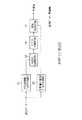
次に、図18は、図1の受信装置4の構成例を示している。 Next, FIG. 18 illustrates a configuration example of the receiving
受信機/再生装置91においては、記録媒体2に記録された符号化データが再生され、または伝送路3を介して伝送されてくる符号化データが受信され、デコード部92に供給される。 In the receiver / reproducing
デコード部92は、図9に示したローカルデコード部27におけるクラス分類用ブロック化回路41乃至予測回路46とそれぞれ同様に構成されるクラス分類用ブロック化回路93乃至予測回路98で構成されており、従って、デコード部92では、図9のローカルデコード部27における場合と同様にして、補正データから予測値が求められ、この予測値で構成される画像が復号画像として出力される。 The decoding unit 92 includes class
即ち、受信機/再生装置91から出力される符号化データとしての補正データは、クラス分類用ブロック化回路93または予測値計算用ブロック化回路94に順次供給され、図9のクラス分類用ブロック化回路41または予測値計算用ブロック化回路42における場合と同様にして、クラス分類用ブロックまたは予測値計算用ブロックに、それぞれブロック化される。そして、クラス分類用ブロックはADRC処理回路95に、予測値計算用ブロックは予測回路98に、それぞれ供給される。 That is, the correction data as the encoded data output from the receiver /
ADRC処理回路95は、クラス分類用ブロックを受信すると、そのクラス分類用ブロックに対して、図9のADRC処理回路43における場合と同様に、1ビットのADRC処理を施し、これにより、クラス分類用ブロックを構成する補正データを、1ビットに変換(符号化)して、クラス分類回路96に出力する。クラス分類回路96は、ADRC処理が施されたクラス分類用ブロックに対して、クラス分類処理を施し、クラス情報を、予測係数ROM97に出力する。 When the
予測係数ROM97は、図9の予測係数ROM45と同様に、例えば、図11の画像処理装置において求められた、クラスごとの予測係数を記憶しており、クラス分類回路96からクラス情報を受信すると、そのクラス情報に対応する予測係数を読み出し、予測回路98に供給する。予測回路98では、予測係数ROM97からの予測係数と、予測値計算用ブロック化回路94からの予測値計算用ブロックを構成する補正データとを用い、式(1)に対応する線形1次式にしたがって、元の画像の予測値が算出され、これにより、元の画像が復号される。 Like the
補正データは、上述したように、誤差情報を所定の閾値以下とするものであり、従って、受信装置4においては、元の画像とほぼ同一の復号画像を得ることができる。 As described above, the correction data has error information that is equal to or less than a predetermined threshold value. Therefore, the receiving
なお、受信側においては、図18に示すような受信装置4でなくても、間引きされた画像を補間により復号する装置により、通常の補間を行うことで復号画像を得ることができる。但し、この場合に得られる復号画像は、画質(解像度)の劣化したものとなる。 On the receiving side, a decoded image can be obtained by performing normal interpolation with a device that decodes the thinned image by interpolation, instead of the receiving
以上、本発明を適用した画像処理装置について説明したが、このような画像処理装置は、例えば、NTSC方式などの標準方式のテレビジョン信号を符号化する場合の他、データ量の多い、いわゆるハイビジョン方式のテレビジョン信号などを符号化する場合に、特に有効である。 The image processing apparatus to which the present invention is applied has been described above. Such an image processing apparatus, for example, encodes a standard system television signal such as the NTSC system, or so-called high vision with a large amount of data. This is particularly effective when encoding a television signal of a system.
なお、本実施の形態においては、1フレームの画像を対象にブロック化を行うようにしたが、ブロックは、その他、例えば、時系列に連続する複数フレームにおける、同一位置の画素などを集めて構成するようにすることも可能である。 In this embodiment, the block is formed on the image of one frame. However, the block is configured by collecting, for example, pixels at the same position in a plurality of frames that are continuous in time series. It is also possible to do so.
また、本実施の形態においては、誤差情報として、誤差の自乗和を用いるようにしたが、誤差情報としては、その他、例えば、誤差の絶対値和や、その3乗以上したものの和などを用いるようにすることが可能である。いずれを誤差情報として用いるかは、例えば、その収束性などに基づいて決定するようにすることが可能である。 In this embodiment, the error sum of squares is used as the error information. However, as the error information, for example, the sum of absolute values of errors or the sum of the third power or more is used. It is possible to do so. Which one is used as error information can be determined based on, for example, its convergence.
さらに、例えば、図13の実施の形態では、1フレーム単位で、正規方程式をたてて、クラスごとの予測係数を求めるようにしたが、予測係数の算出処理は、その他、例えば、1フィールド単位や複数フレーム単位で正規方程式をたてて行うようにすることも可能である。他の処理についても同様である。 Furthermore, for example, in the embodiment shown in FIG. 13, a normal equation is created in units of one frame and the prediction coefficient for each class is obtained. It is also possible to construct a normal equation in units of multiple frames. The same applies to other processes.
また、本発明は、ハードウェアによっても、あるいは、上述した処理を行うためのアプリケーションプログラムが記録されたハードディスク等の記録媒体から、そのアプリケーションプログラムを読み出して、コンピュータに実行させることによっても、実現可能である。 The present invention can also be realized by hardware or by reading the application program from a recording medium such as a hard disk in which the application program for performing the above-described processing is recorded and causing the computer to execute it. It is.
さらに、図2においては、ADRC処理回路12に供給するブロックと、遅延回路15を介して、演算回路16に供給するブロックとは同一のものとしたが、これらのブロックは同一である必要は必ずしもない。 Further, in FIG. 2, the block supplied to the
1 送信装置, 2 記録媒体, 3 伝送路, 4 受信装置, 11 ブロック化回路, 12 ADRC処理回路, 13 クラス分類回路, 14 マッピング係数メモリ, 15 遅延回路, 16 演算回路, 17 送信機/記録装置, 21 メモリ, 22 ブロック化回路, 23 ADRC処理回路, 24 クラス分類回路, 26 演算回路, 27 ローカルデコード部, 28 誤差算出部, 29 判定部, 30 マッピング係数設定回路, 31 マッピング係数メモリ, 41 クラス分類用ブロック化回路, 42 予測値計算用ブロック化回路, 43 ADRC処理回路, 44 クラス分類回路, 45 予測係数ROM, 46 予測回路, 47 適応処理回路, 51 学習用ブロック化回路, 52 教師用ブロック化回路, 53 ADRC処理回路, 54 クラス分類回路, 55 スイッチ, 56 学習データメモリ, 57 カウンタ, 58 教師データメモリ, 59 演算回路, 60 メモリ, 70 最適補正データ算出部, 71 圧縮部, 72 補正部, 73 ローカルデコード部, 74 誤差算出部, 75 判定部, 76 ラッチ回路, 76A メモリ, 77 ブロック化回路, 77A メモリ, 78 ADRC処理回路, 79 クラス分類回路, 80 メモリ, 81 演算回路, 82 メモリ, 91 受信機/再生装置, 92 デコード部, 93 クラス分類用ブロック化回路, 94 予測値計算用ブロック化回路, 95 ADRC処理回路, 96 クラス分類回路, 97 予測係数ROM, 98 予測回路, 1027 ローカルデコード部 DESCRIPTION OF SYMBOLS 1 Transmitter, 2 Recording medium, 3 Transmission path, 4 Receiver, 11 Blocking circuit, 12 ADRC processing circuit, 13 Class classification circuit, 14 Mapping coefficient memory, 15 Delay circuit, 16 Arithmetic circuit, 17 Transmitter / recording device , 21 memory, 22 blocking circuit, 23 ADRC processing circuit, 24 class classification circuit, 26 arithmetic circuit, 27 local decoding unit, 28 error calculation unit, 29 determination unit, 30 mapping coefficient setting circuit, 31 mapping coefficient memory, 41 class Classification block circuit, 42 Predictive value calculation block circuit, 43 ADRC processing circuit, 44 class classification circuit, 45 prediction coefficient ROM, 46 prediction circuit, 47 adaptive processing circuit, 51 learning block circuit, 52 teacher block Circuit, 53 ADRC processing circuit, 54 class classification circuit, 55 switch, 56 learning data memory, 57 counter, 58 teacher data memory, 59 arithmetic circuit, 60 memory, 70 optimum correction data calculation unit, 71 compression unit, 72 correction unit, 73 local Decoding unit, 74 error calculation unit, 75 determination unit, 76 latch circuit, 76A memory, 77 block circuit, 77A memory, 78 ADRC processing circuit, 79 class classification circuit, 80 memory, 81 arithmetic circuit, 82 memory, 91 receiver / Playback device, 92 decoding unit, 93 class classification blocking circuit, 94 prediction value calculation blocking circuit, 95 ADRC processing circuit, 96 class classification circuit, 97 prediction coefficient ROM, 98 prediction circuit, 1027 local Code section
Claims (3)
Translated fromJapanese前記画像符号化装置は、
前記画像を構成する画素から注目している注目画素周辺の複数の画素を抽出し、抽出された前記複数の画素の性質に応じて前記注目画素を第1のクラスに分類する分類手段と、
前記第1のクラスごとに、前記画像を符号化するための所定のマッピング係数を記憶しているマッピング係数記憶手段と、
前記画像の中の、注目している前記注目画素周辺の複数の画素と、前記注目画素の第1のクラスに対応する前記マッピング係数とを引数とする所定の関数の演算を行うことにより、符号化された前記注目画素を、前記注目画素周辺の複数の画素の符号化データとして出力する演算手段と
を備え、
前記画像復号化装置は、
前記画像符号化装置で符号化させた前記符号化データを受信する受信手段と、
前記符号化データを復号化する復号化手段と
を備え、
前記復号化手段は、
前記符号化データを、その性質に応じて第2のクラスのうちのいずれかに分類する分類手段と、
前記符号化データの前記第2のクラスに対応する、前記符号化データから予測される元の画像の予測値を算出するための予測係数と、前記符号化データとの線形結合により、前記予測値を求める予測値演算手段と
を有する
ことを特徴とする画像処理システム。An image processing system comprising an image encoding device for encoding an image and an image decoding device for decoding the encoded image,
The image encoding device includes:
Classifying means for extractinga plurality of pixels arounda target pixel of interest from pixels constituting the image, and classifying the target pixel into a first class according to properties of the extracted pixels;
Mapping coefficient storage means for storing a predetermined mapping coefficient for encoding the image for each of the first classes;
In said image, a plurality of pixelsaround the target pixel of interest, by performing the calculation of a predetermined function to the said mapping coefficients argument corresponding to the first class of the pixel of interest,code And calculating means for outputting theconverted targetpixel as encoded data ofa plurality of pixels around the targetpixel ,
The image decoding device includes:
Receiving means for receiving the encoded data encoded by the image encoding device;
Decoding means for decoding the encoded data,
The decoding means includes
Classification means for classifying the encoded data into any one of the second classes according to the property;
The predicted value by linear combination of a prediction coefficient corresponding to the second class of the encoded data and for calculating a predicted value of an original image predicted from the encoded data, and the encoded data Predicted value calculation means for obtaining
Have
An image processing system characterized by that.
ことを特徴とする請求項1に記載の画像処理システム。The arithmetic means calculatesthe number of pixels of the image by using the encoded pixel of interest as the encoded data ofa plurality of pixels aroundthe pixel of interest. Item 8. The image processing system according to Item 1.
前記予測係数を、前記第2のクラスごとに記憶している予測係数記憶手段をさらに備える
ことを特徴とする請求項2に記載の画像処理システム。The decoding means includes
The prediction coefficients,further comprising a prediction coefficient storage means for storing for each ofthe second class
The image processing system according to claim 2.
Priority Applications (1)
| Application Number | Priority Date | Filing Date | Title |
|---|---|---|---|
| JP2005309781AJP4487900B2 (en) | 1996-07-17 | 2005-10-25 | Image processing system |
Applications Claiming Priority (2)
| Application Number | Priority Date | Filing Date | Title |
|---|---|---|---|
| JP20655396 | 1996-07-17 | ||
| JP2005309781AJP4487900B2 (en) | 1996-07-17 | 2005-10-25 | Image processing system |
Related Parent Applications (1)
| Application Number | Title | Priority Date | Filing Date |
|---|---|---|---|
| JP20849897ADivisionJP3912558B2 (en) | 1996-07-17 | 1997-07-17 | Image encoding apparatus, image encoding method, and recording medium |
Publications (2)
| Publication Number | Publication Date |
|---|---|
| JP2006115526A JP2006115526A (en) | 2006-04-27 |
| JP4487900B2true JP4487900B2 (en) | 2010-06-23 |
Family
ID=36383554
Family Applications (1)
| Application Number | Title | Priority Date | Filing Date |
|---|---|---|---|
| JP2005309781AExpired - Fee RelatedJP4487900B2 (en) | 1996-07-17 | 2005-10-25 | Image processing system |
Country Status (1)
| Country | Link |
|---|---|
| JP (1) | JP4487900B2 (en) |
- 2005
- 2005-10-25JPJP2005309781Apatent/JP4487900B2/ennot_activeExpired - Fee Related
Also Published As
| Publication number | Publication date |
|---|---|
| JP2006115526A (en) | 2006-04-27 |
Similar Documents
| Publication | Publication Date | Title |
|---|---|---|
| US6266454B1 (en) | Device and method for processing, image and device and method for encoding image | |
| JP3912627B2 (en) | Image coding apparatus, image coding method, and transmission method | |
| JP4126709B2 (en) | Image processing apparatus and image processing method | |
| JP3915855B2 (en) | Image coding apparatus, image coding method, learning apparatus, and learning method | |
| AU714554B2 (en) | Image coding and decoding using mapping coefficients corresponding to class information of pixel blocks | |
| KR100574732B1 (en) | Image coding apparatus, image coding method, image decoding method, image decoding apparatus, image data transmitting method and recording medium | |
| KR100537123B1 (en) | Picture signal coding device, picture signal coding method, picture signal decoding device, picture signal decoding method, and recording medium | |
| JP3912558B2 (en) | Image encoding apparatus, image encoding method, and recording medium | |
| WO1998030028A1 (en) | Picture coding device, picture coding method, picture decoding device, picture decoding method, and recording medium | |
| JP3747970B2 (en) | Image encoding device, image encoding method, image decoding device, and image decoding method | |
| JP4487900B2 (en) | Image processing system | |
| JP3844031B2 (en) | Image coding apparatus and image coding method, and image decoding apparatus and image decoding method | |
| JP3912628B2 (en) | Image encoding device, image encoding method, image encoding and decoding system, image encoding and decoding method, and recording medium | |
| JP3912629B2 (en) | Image processing system, image encoding device, image encoding method, transmission method, and recording medium | |
| JP4534951B2 (en) | Image coding apparatus, image coding method, image processing system, image processing method, transmission method, and recording medium | |
| JPH10243405A (en) | Image signal coder, image signal coding method, image signal decoder, image signal decoding method and recording medium | |
| JP4582416B2 (en) | Image coding apparatus and image coding method | |
| KR100598754B1 (en) | Device for coding original image data, device for decoding coded image data, method for coding original image data, method for decoding coded image data, method for transmitting image data, computer-readable storing media | |
| JP3952326B2 (en) | Image coding apparatus, image coding method, image processing system, image processing method, transmission method, and recording medium | |
| JP4496494B2 (en) | Image coding apparatus and image coding method | |
| EP1298934A1 (en) | Apparatus and method for image coding and decoding | |
| JP4566877B2 (en) | Image processing apparatus and method | |
| JP4807349B2 (en) | Learning apparatus and method |
Legal Events
| Date | Code | Title | Description |
|---|---|---|---|
| A131 | Notification of reasons for refusal | Free format text:JAPANESE INTERMEDIATE CODE: A131 Effective date:20090217 | |
| A521 | Written amendment | Free format text:JAPANESE INTERMEDIATE CODE: A523 Effective date:20090420 | |
| TRDD | Decision of grant or rejection written | ||
| A01 | Written decision to grant a patent or to grant a registration (utility model) | Free format text:JAPANESE INTERMEDIATE CODE: A01 Effective date:20100309 | |
| A01 | Written decision to grant a patent or to grant a registration (utility model) | Free format text:JAPANESE INTERMEDIATE CODE: A01 | |
| A61 | First payment of annual fees (during grant procedure) | Free format text:JAPANESE INTERMEDIATE CODE: A61 Effective date:20100322 | |
| FPAY | Renewal fee payment (event date is renewal date of database) | Free format text:PAYMENT UNTIL: 20130409 Year of fee payment:3 | |
| FPAY | Renewal fee payment (event date is renewal date of database) | Free format text:PAYMENT UNTIL: 20130409 Year of fee payment:3 | |
| FPAY | Renewal fee payment (event date is renewal date of database) | Free format text:PAYMENT UNTIL: 20140409 Year of fee payment:4 | |
| R250 | Receipt of annual fees | Free format text:JAPANESE INTERMEDIATE CODE: R250 | |
| R250 | Receipt of annual fees | Free format text:JAPANESE INTERMEDIATE CODE: R250 | |
| LAPS | Cancellation because of no payment of annual fees |