JP4484345B2 - Semiconductor device and manufacturing method thereof - Google Patents
Semiconductor device and manufacturing method thereofDownload PDFInfo
- Publication number
- JP4484345B2 JP4484345B2JP2000274426AJP2000274426AJP4484345B2JP 4484345 B2JP4484345 B2JP 4484345B2JP 2000274426 AJP2000274426 AJP 2000274426AJP 2000274426 AJP2000274426 AJP 2000274426AJP 4484345 B2JP4484345 B2JP 4484345B2
- Authority
- JP
- Japan
- Prior art keywords
- film
- insulating layer
- semiconductor device
- layer
- atoms
- Prior art date
- Legal status (The legal status is an assumption and is not a legal conclusion. Google has not performed a legal analysis and makes no representation as to the accuracy of the status listed.)
- Expired - Fee Related
Links
- 239000004065semiconductorSubstances0.000titleclaimsdescription43
- 238000004519manufacturing processMethods0.000titleclaimsdescription20
- 238000005530etchingMethods0.000claimsdescription90
- 239000004020conductorSubstances0.000claimsdescription39
- 229910052710siliconInorganic materials0.000claimsdescription37
- 229910052799carbonInorganic materials0.000claimsdescription35
- 229910052751metalInorganic materials0.000claimsdescription35
- 239000002184metalSubstances0.000claimsdescription35
- 229910052757nitrogenInorganic materials0.000claimsdescription34
- 238000000034methodMethods0.000claimsdescription32
- 230000004888barrier functionEffects0.000claimsdescription16
- 125000004429atomChemical group0.000claimsdescription13
- 125000004433nitrogen atomChemical groupN*0.000claimsdescription12
- 125000004432carbon atomChemical groupC*0.000claimsdescription11
- ABTOQLMXBSRXSM-UHFFFAOYSA-Nsilicon tetrafluorideChemical compoundF[Si](F)(F)FABTOQLMXBSRXSM-UHFFFAOYSA-N0.000claimsdescription6
- TXEYQDLBPFQVAA-UHFFFAOYSA-NtetrafluoromethaneChemical compoundFC(F)(F)FTXEYQDLBPFQVAA-UHFFFAOYSA-N0.000claimsdescription6
- 238000005498polishingMethods0.000claimsdescription4
- 239000010410layerSubstances0.000description97
- 239000007789gasSubstances0.000description40
- 150000001875compoundsChemical class0.000description19
- 229910020177SiOFInorganic materials0.000description10
- 230000015572biosynthetic processEffects0.000description10
- 238000010586diagramMethods0.000description10
- 238000009792diffusion processMethods0.000description10
- 239000011229interlayerSubstances0.000description9
- 230000008569processEffects0.000description8
- 239000000758substrateSubstances0.000description8
- 229910052731fluorineInorganic materials0.000description7
- 239000011737fluorineSubstances0.000description7
- 238000005268plasma chemical vapour depositionMethods0.000description7
- 238000002156mixingMethods0.000description6
- 238000001020plasma etchingMethods0.000description6
- 239000000203mixtureSubstances0.000description5
- 238000002161passivationMethods0.000description5
- 238000001004secondary ion mass spectrometryMethods0.000description5
- YCKRFDGAMUMZLT-UHFFFAOYSA-NFluorine atomChemical compound[F]YCKRFDGAMUMZLT-UHFFFAOYSA-N0.000description4
- 239000002994raw materialSubstances0.000description4
- 229910004298SiO 2Inorganic materials0.000description3
- 239000000956alloySubstances0.000description3
- 229910045601alloyInorganic materials0.000description3
- 230000009977dual effectEffects0.000description3
- 230000004048modificationEffects0.000description3
- 238000012986modificationMethods0.000description3
- 238000004544sputter depositionMethods0.000description3
- 150000001343alkyl silanesChemical class0.000description2
- 238000005229chemical vapour depositionMethods0.000description2
- 230000007423decreaseEffects0.000description2
- FFUAGWLWBBFQJT-UHFFFAOYSA-NhexamethyldisilazaneChemical compoundC[Si](C)(C)N[Si](C)(C)CFFUAGWLWBBFQJT-UHFFFAOYSA-N0.000description2
- 239000012528membraneSubstances0.000description2
- 238000005001rutherford backscattering spectroscopyMethods0.000description2
- 150000004756silanesChemical class0.000description2
- 230000007480spreadingEffects0.000description2
- 238000003892spreadingMethods0.000description2
- 239000000126substanceSubstances0.000description2
- NMVVEFUHHZJTPM-UHFFFAOYSA-N2,2,4,4,6,6,8,8-octaethyl-1,3,5,7,2,4,6,8-tetrazatetrasilocaneChemical compoundCC[Si]1(CC)N[Si](CC)(CC)N[Si](CC)(CC)N[Si](CC)(CC)N1NMVVEFUHHZJTPM-UHFFFAOYSA-N0.000description1
- FIADVASZMLCQIF-UHFFFAOYSA-N2,2,4,4,6,6,8,8-octamethyl-1,3,5,7,2,4,6,8-tetrazatetrasilocaneChemical compoundC[Si]1(C)N[Si](C)(C)N[Si](C)(C)N[Si](C)(C)N1FIADVASZMLCQIF-UHFFFAOYSA-N0.000description1
- DFQSCSITPYBDDC-UHFFFAOYSA-N2,2,4,4,6,6-hexaethyl-1,3,5,2,4,6-triazatrisilinaneChemical compoundCC[Si]1(CC)N[Si](CC)(CC)N[Si](CC)(CC)N1DFQSCSITPYBDDC-UHFFFAOYSA-N0.000description1
- SHWQWXGIWFEYTA-UHFFFAOYSA-N2,2,4,4,6,6-hexakis-phenyl-1,3,5,2,4,6-triazatrisilinaneChemical compoundN1[Si](C=2C=CC=CC=2)(C=2C=CC=CC=2)N[Si](C=2C=CC=CC=2)(C=2C=CC=CC=2)N[Si]1(C=1C=CC=CC=1)C1=CC=CC=C1SHWQWXGIWFEYTA-UHFFFAOYSA-N0.000description1
- WGGNJZRNHUJNEM-UHFFFAOYSA-N2,2,4,4,6,6-hexamethyl-1,3,5,2,4,6-triazatrisilinaneChemical compoundC[Si]1(C)N[Si](C)(C)N[Si](C)(C)N1WGGNJZRNHUJNEM-UHFFFAOYSA-N0.000description1
- VXCKEYPCWKTAFO-UHFFFAOYSA-N2,4,6,8-tetraethyl-1,3,5,7-tetramethyl-1,3,5,7,2,4,6,8-tetrazatetrasilocaneChemical compoundCC[SiH]1N(C)[SiH](CC)N(C)[SiH](CC)N(C)[SiH](CC)N1CVXCKEYPCWKTAFO-UHFFFAOYSA-N0.000description1
- JGTIYBGFHLZUEU-UHFFFAOYSA-N2,4,6-triethyl-1,3,5-trimethyl-1,3,5,2,4,6-triazatrisilinaneChemical compoundCC[SiH]1N(C)[SiH](CC)N(C)[SiH](CC)N1CJGTIYBGFHLZUEU-UHFFFAOYSA-N0.000description1
- BSYNRYMUTXBXSQ-UHFFFAOYSA-NAspirinChemical compoundCC(=O)OC1=CC=CC=C1C(O)=OBSYNRYMUTXBXSQ-UHFFFAOYSA-N0.000description1
- AYDSPSJZGVYVNL-UHFFFAOYSA-NC=1C=CC=CC=1[SiH](N(C)[Si](C)(C)C)C1=CC=CC=C1Chemical compoundC=1C=CC=CC=1[SiH](N(C)[Si](C)(C)C)C1=CC=CC=C1AYDSPSJZGVYVNL-UHFFFAOYSA-N0.000description1
- OKTJSMMVPCPJKN-UHFFFAOYSA-NCarbonChemical compound[C]OKTJSMMVPCPJKN-UHFFFAOYSA-N0.000description1
- RMIMDWDBQJHCEV-UHFFFAOYSA-NN-dibutylsilyl-N-trimethylsilylmethanamineChemical compoundCCCC[SiH](N(C)[Si](C)(C)C)CCCCRMIMDWDBQJHCEV-UHFFFAOYSA-N0.000description1
- VJFUNCKASZQOPO-UHFFFAOYSA-NN-dioctylsilyl-N-trimethylsilylmethanamineChemical compoundCCCCCCCC[SiH](N(C)[Si](C)(C)C)CCCCCCCCVJFUNCKASZQOPO-UHFFFAOYSA-N0.000description1
- LCMQDEJHSONROR-UHFFFAOYSA-NN-dipropylsilyl-N-trimethylsilylmethanamineChemical compoundCCC[SiH](CCC)N(C)[Si](C)(C)CLCMQDEJHSONROR-UHFFFAOYSA-N0.000description1
- BLRPTPMANUNPDV-UHFFFAOYSA-NSilaneChemical compound[SiH4]BLRPTPMANUNPDV-UHFFFAOYSA-N0.000description1
- ATJFFYVFTNAWJD-UHFFFAOYSA-NTinChemical compound[Sn]ATJFFYVFTNAWJD-UHFFFAOYSA-N0.000description1
- GJWAPAVRQYYSTK-UHFFFAOYSA-N[(dimethyl-$l^{3}-silanyl)amino]-dimethylsiliconChemical compoundC[Si](C)N[Si](C)CGJWAPAVRQYYSTK-UHFFFAOYSA-N0.000description1
- APDDLLVYBXGBRF-UHFFFAOYSA-N[diethyl-(triethylsilylamino)silyl]ethaneChemical compoundCC[Si](CC)(CC)N[Si](CC)(CC)CCAPDDLLVYBXGBRF-UHFFFAOYSA-N0.000description1
- UDWMDYGDGBKDJC-UHFFFAOYSA-N[dimethyl-(triphenylsilylamino)silyl]benzeneChemical compoundC1(=CC=CC=C1)[Si](N[Si](C)(C)C1=CC=CC=C1)(C1=CC=CC=C1)C1=CC=CC=C1UDWMDYGDGBKDJC-UHFFFAOYSA-N0.000description1
- TWSOFXCPBRATKD-UHFFFAOYSA-N[diphenyl-(triphenylsilylamino)silyl]benzeneChemical compoundC=1C=CC=CC=1[Si](C=1C=CC=CC=1)(C=1C=CC=CC=1)N[Si](C=1C=CC=CC=1)(C=1C=CC=CC=1)C1=CC=CC=C1TWSOFXCPBRATKD-UHFFFAOYSA-N0.000description1
- 238000006243chemical reactionMethods0.000description1
- NEHMKBQYUWJMIP-UHFFFAOYSA-NchloromethaneChemical compoundClCNEHMKBQYUWJMIP-UHFFFAOYSA-N0.000description1
- 238000001514detection methodMethods0.000description1
- UBHZUDXTHNMNLD-UHFFFAOYSA-NdimethylsilaneChemical compoundC[SiH2]CUBHZUDXTHNMNLD-UHFFFAOYSA-N0.000description1
- 230000000694effectsEffects0.000description1
- 238000007772electroless platingMethods0.000description1
- 125000001495ethyl groupChemical group[H]C([H])([H])C([H])([H])*0.000description1
- 230000002349favourable effectEffects0.000description1
- 238000010438heat treatmentMethods0.000description1
- 230000001939inductive effectEffects0.000description1
- 238000011835investigationMethods0.000description1
- 238000001459lithographyMethods0.000description1
- 239000000463materialSubstances0.000description1
- 150000002739metalsChemical class0.000description1
- 125000002496methyl groupChemical group[H]C([H])([H])*0.000description1
- UIUXUFNYAYAMOE-UHFFFAOYSA-NmethylsilaneChemical compound[SiH3]CUIUXUFNYAYAMOE-UHFFFAOYSA-N0.000description1
- ZSMNRKGGHXLZEC-UHFFFAOYSA-Nn,n-bis(trimethylsilyl)methanamineChemical compoundC[Si](C)(C)N(C)[Si](C)(C)CZSMNRKGGHXLZEC-UHFFFAOYSA-N0.000description1
- WKWOFMSUGVVZIV-UHFFFAOYSA-Nn-bis(ethenyl)silyl-n-trimethylsilylmethanamineChemical compoundC[Si](C)(C)N(C)[SiH](C=C)C=CWKWOFMSUGVVZIV-UHFFFAOYSA-N0.000description1
- -1n-octyl groupChemical group0.000description1
- 239000011368organic materialSubstances0.000description1
- 238000000059patterningMethods0.000description1
- 125000001997phenyl groupChemical group[H]C1=C([H])C([H])=C(*)C([H])=C1[H]0.000description1
- 238000000206photolithographyMethods0.000description1
- 238000007747platingMethods0.000description1
- 238000003672processing methodMethods0.000description1
- 125000001436propyl groupChemical group[H]C([*])([H])C([H])([H])C([H])([H])[H]0.000description1
- 239000011241protective layerSubstances0.000description1
- 239000003870refractory metalSubstances0.000description1
- 229910000077silaneInorganic materials0.000description1
- LIVNPJMFVYWSIS-UHFFFAOYSA-Nsilicon monoxideChemical class[Si-]#[O+]LIVNPJMFVYWSIS-UHFFFAOYSA-N0.000description1
- 229910052814silicon oxideInorganic materials0.000description1
- 238000009751slip formingMethods0.000description1
- CZDYPVPMEAXLPK-UHFFFAOYSA-NtetramethylsilaneChemical compoundC[Si](C)(C)CCZDYPVPMEAXLPK-UHFFFAOYSA-N0.000description1
- 238000012719thermal polymerizationMethods0.000description1
- TUQLLQQWSNWKCF-UHFFFAOYSA-NtrimethoxymethylsilaneChemical compoundCOC([SiH3])(OC)OCTUQLLQQWSNWKCF-UHFFFAOYSA-N0.000description1
- PQDJYEQOELDLCP-UHFFFAOYSA-NtrimethylsilaneChemical compoundC[SiH](C)CPQDJYEQOELDLCP-UHFFFAOYSA-N0.000description1
Images


Landscapes
- Internal Circuitry In Semiconductor Integrated Circuit Devices (AREA)
- Formation Of Insulating Films (AREA)
Description
Translated fromJapanese【0001】
【発明の属する技術分野】
本発明は、半導体装置及び半導体装置の製造方法に関する。
【0002】
【従来の技術】
半導体集積回路の高性能化のために、配線の高速化が進められている。配線の高速化には、層間絶縁膜の低誘電率化及び配線抵抗の低減が有効な手段である。低誘電率の層間絶縁膜としては、SiOF膜(約3.5)等が従来のSiO2膜(約4.0)に代わって用いられている。また、配線抵抗の低減のため、従来のAl(抵抗率2.7μΩ・cm)を主成分とする合金よりも、エレクトロマイグレーション耐性に優れ、低抵抗な(1.9μΩ・cm)Cuを配線金属として用いることが多くなっている。
【0003】
Cu配線を使用する場合、従来のエッチングプロセスによる加工が困難であるため、CuをエッチングせずにCuの多層配線を実現する方法として、所謂ダマシン法が用いられている。以下、図11(a)〜(f)を参照して、ダマシン法を説明する。
【0004】
まず、基板又は下層配線層601上に、例えば、SiOFから構成される層間絶縁膜(下地膜)602、エッチングストッパ膜603を順に形成する(図11(a))。次いで、基板表面上に開口604aを有するレジストパターン604を設け(図11(b))、これをマスクとしてプラズマエッチング等により、エッチングストッパ膜603にスルーホール603aを形成する(図11(c))。さらに、スルーホール603aの形成されたエッチングストッパ膜603をマスクとしたパターニングにより配線溝605を形成する(図11(d))。続いて、金属膜606の密着層であるバリヤメタル膜606aをスパッタリング等によって形成した後、金属膜606をめっき等により形成する(図11(e))。その後、化学的機械的研磨(Chemical Mechanical Polishing:CMP)により、エッチングストッパ膜603をストッパとして不用なバリヤメタル膜及び金属膜の除去を行うとともに、表面を平坦化する(図11(f))。以上のような工程によって、配線層が形成され、この工程を繰り返して多層配線層が形成される。
【0005】
【発明が解決しようとする課題】
上記したダマシン法では、エッチングストッパ膜が用いられ、このエッチングストッパ膜は、下地膜のエッチングにおいてはマスクとして働く。従って、下地膜との高いエッチング選択比が求められる。また、エッチングストッパ膜は、半導体装置中で層間絶縁膜としての働きも有するので、低い比誘電率、そして、配線金属がCuである場合には特に、低い金属拡散性が求められる。
【0006】
このようなエッチングストッパ膜としては、SiとNを主要元素として構成されるもの(以下、SiN系膜)、SiとCを主要元素として構成されるもの(以下、SiC系膜)が知られている。しかしながら、SiN系膜の比誘電率は7〜8と高いものである。さらに、下地膜がSiOF等のフッ素含有膜であり、これをプラズマエッチングする場合には、エッチング時に発生したフッ素ラジカル等によってSiN系膜が損傷するなど、エッチング選択比が十分に取れず、加工精度が劣化する。また、SiC系膜(特に、CHn基を含む膜)は、エッチング選択比が良好であり、比誘電率が5付近のものもあるが、Cuの拡散性が高い。このように、従来のエッチングストッパ膜は、ダマシン法による配線構造の形成に必要な条件を十分に満たしてはいなかった。
【0007】
従って、本発明は、信頼性の高い半導体装置及びその製造方法の提供を目的とする。
【0008】
【課題を解決するための手段】
上記目的を達成するため、本発明の第1の観点に係る半導体装置は、複数の溝又は穴を有する低誘電率の第1の絶縁層と、前記第1の絶縁層上に形成され、前記複数の溝又は穴と重なる複数の開口を有し、SiとCとNとを主たる含有元素とする第2の絶縁層と、前記複数の溝又は穴と前記複数の開口とから形成される複数の配線溝又は穴に埋め込まれた導体層と、を備え、前記第1の絶縁層は、フッ化酸化ケイ素又はフッ化カーボンから構成される、ことを特徴とする。
【0009】
上記構成によれば、SiとCとNとから構成される第2の絶縁層は、従来の、SiとC又はSiとNとから構成されるエッチングストッパ膜と比べて同等又はそれ以下の誘電率を有するとともに、これらのエッチングストッパ膜に比べて、第1の絶縁膜との良好なエッチング選択比を有している。このため、信頼性の高い半導体装置が提供される。
【0010】
上記構成において、前記第2の絶縁層は、Si原子の数に対するC原子の数の比が0.2〜0.8であり、かつ、Si原子の数に対するN原子の数の比が0.15〜1.0であることが好ましい。SiCN系膜中のSi、C、Nの存在比が上記範囲にある場合、SiCN膜の前記第1の絶縁層に対するエッチング選択比は高く、かつ、Cu拡散性も低減される。
【0011】
上記構成において、前記第1の絶縁層は、フッ化酸化ケイ素又はフッ化カーボンから構成されている。これらのフッ素含有膜は、プラズマエッチングに際し、フッ素ラジカル等の発生を伴う。しかし、SiCN系の前記第2の絶縁層(エッチングストッパ膜)はこれらのラジカルに強く、前記第1の絶縁層に対してエッチング選択比を十分に取れる。
【0012】
上記構成において、前記導体層は、Cuから構成されていてもよい。すなわち、SiとCとNとから構成される第2の絶縁層はCu拡散性が低いので、Cuを用いた、信頼性の高い配線層が形成される。
【0013】
上記構成において、前記配線溝又は穴にはバリアメタル層が形成され、前記導体層は、前記バリアメタル層の上に形成されていることが好ましい。この構成により、導体層を構成する金属の拡散を抑止することができるだけでなく、導体層と層間絶縁層との密着性を高めることができ、半導体装置の信頼性を向上させることができる。
【0014】
上記構成において、さらに、前記第2の絶縁層及び前記導体層の上に形成され、SiとCとNとを主たる含有元素とする第3の絶縁層を備えることが好ましい。これにより、Cu等の導体層からの金属の拡散を抑えることができる。
【0015】
上記目的を達成するため、本発明の第2の観点に係る半導体装置の製造方法は、第1の絶縁層を形成する工程と、前記第1の絶縁層上に、SiとCとNとを主たる含有元素とする第2の絶縁層を形成する工程と、前記第1の絶縁層の表面が部分的に露出するよう、前記第2の絶縁層を選択的にエッチングして開口を形成する工程と、前記選択的にエッチングされた第2の絶縁層をマスクとして前記第1の絶縁層をエッチングして、配線溝又は穴を形成する工程と、前記開口及び前記配線溝又は穴を埋めて導体層を形成する工程と、前記導体層を、前記第2の絶縁層をストッパとして研磨する工程と、を備え、前記第1の絶縁層は、フッ化酸化ケイ素又はフッ化カーボンから構成される、ことを特徴とする。
【0016】
上記構成によれば、SiとCとNとから構成される第2の絶縁層は、従来の、SiとC又はSiとNとから構成されるエッチングストッパ膜と比べて同等又はそれ以下の誘電率を有するとともに、これらのエッチングストッパ膜に比べて、一般的な層間絶縁膜である第1の絶縁層との良好なエッチング選択比を有する。このため、信頼性の高い半導体装置の製造することができる。
【0017】
上記構成において、前記第2の絶縁層は、Si原子の数に対するC原子の数の比が0.2〜0.8であり、かつ、Si原子の数に対するN原子の数の比が0.15〜1.0であることが好ましい。SiCN系膜中のSi、C、Nの存在比が上記範囲にある場合、SiCN膜の下地膜に対するエッチング選択比は高く、かつ、Cu拡散性も低減される。
【0018】
上記構成において、前記第1の絶縁層は、フッ化酸化ケイ素又はフッ化カーボンから構成されている。これらのフッ素含有膜は、プラズマエッチングに際し、フッ素ラジカル等の発生を伴う。しかし、SiCN系の前記第2の絶縁層(エッチングストッパ膜)はこれらのラジカルに強く、前記第1の絶縁層に対してエッチング選択比を十分に取れる。
【0019】
上記構成において、前記導体層は、Cuから構成されていてもよい。すなわち、SiとCとNとから構成される第2の絶縁層はCu拡散性が低いので、Cuを用いた、信頼性の高い配線層が形成される。
【0020】
上記構成において、さらに、前記導体層と、前記開口及び前記配線溝又は穴との間にバリアメタル層を形成する工程を備えることが好ましい。この構成により、導体層を構成する金属の拡散を抑止することができるだけでなく、導体層と層間絶縁層との密着性を高めることができ、半導体装置の信頼性を向上させることができる。
【0021】
上記構成において、さらに、前記第2の絶縁層及び前記導体層の上に、SiとCとNとを主たる含有元素とする第3の絶縁層を形成する工程を備えることが好ましい。これにより、Cu等の導体層からの金属の拡散を抑えることができる。
【0022】
【発明の実施の形態】
本発明の実施の形態にかかる半導体装置について、以下図面を参照して説明する。
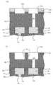
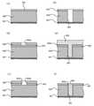
図1は、本実施の形態の半導体装置の構成を示す部分断面図である。この半導体装置は、Si等の基板上に形成されたMOSトランジスタ等の素子を覆う絶縁膜(図示せず)上に多層配線層を形成したものであり、図1は、基板表面に形成された配線層を示している。
【0023】
図1に示すように、最上層の配線層HLの下に、第1の下地膜(層間絶縁膜)101、第1の導体層102、第1のエッチングストッパ膜105、から構成される下層配線層LLが形成されている。
【0024】
第1の下地膜101は、フッ化酸化ケイ素(SiOF)膜、フッ素含有カーボン膜等から構成され、第1のエッチングストッパ膜105とともに、第1のトレンチホール103及び第1のビアホール104を形成している。形成された第1のトレンチホール103及び第1のビアホール104には第1の導体層102が形成されている。第1の導体層102は、Cu等の導体から構成される。第1の下地膜101と第1の導体層102との間には、第1のバリアメタル膜102aが形成される。第1のバリアメタル膜102aは、Ta/TaN、W/WN、Ti/TiN等の高融点金属又はその金属の合金の多層膜から構成され、Cu等の金属の拡散を防ぐとともに、下地膜101と導体層102との密着性を高める機能を持つ。第1の導体層102は、さらに下の配線層(図示せず)又はSi基板に接続されている。
【0025】
第1のエッチングストッパ膜105は、SiとCとNとを主要元素として構成されたSiCN系の絶縁膜である。このSiCN系膜は、C原子の数のSi原子の数に対する比(C/Si)が0.2〜0.8、かつ、N原子の数のSi原子の数に対する比(N/Si)が0.15〜1.0であるように組成されている。また、このSiCN系膜の比誘電率は5〜5.5であり、エッチングストッパ膜として知られているSiN系(SiとNを主要元素とする)膜(7付近)よりも低く、SiC系(SiとCを主要元素とする)膜(5付近)と同程度に低い。
【0026】
上述の下層配線層LLの上には、第2の下地膜106及び第2のエッチングストッパ膜110が形成されている。下層配線層LLと同様に、第2の下地膜106及び第2のエッチングストッパ膜110は、第2のトレンチホール108及び第2のビアホール109を形成し、これらの内部には、第2のバリアメタル膜107aを介して、第2の導体層107が埋め込まれている。
【0027】
最上層の配線層HLの上には、第3のエッチングストッパ膜111が形成され、これは、SiとCとNとを主要元素として構成された上記第1及び第2のエッチングストッパ膜と同じ構成を有し、Cu等からなる導体層からの金属の拡散を抑える機能を有する。さらに第3のエッチングストッパ膜111の上には、第3の下地膜112及びパッシベーション膜113(例えば、SiO2膜、SiON膜)が順に形成されている。これらは、酸化等されやすい基板表面の保護層である。
【0028】
次に、上述した半導体装置の製造方法を説明する。本実施の形態では、半導体装置を、ダマシン法の変形である、トレンチホールとビアホールを形成する、デュアルダマシン法を用いて製造する。
【0029】
図2〜図6は、デュアルダマシン法によるCu配線の形成工程を順に示す図である。以下、図を参照して順次説明を行う。
【0030】
まず、図2(a)に示すように、第1の下地膜101、第1の導体層102、第1のエッチングストッパ膜105等から構成される下層配線層LL上に、第2の下地膜106、第2のエッチングストッパ膜110を順次成膜する。第2の下地膜106は、SiOF膜であり、電子サイクロトロン共鳴(Electron Cyclotron Resonance:ECR)プラズマを用いる化学的気相成長法(Chemical Vapor Deposition:CVD)により、例えば、SiH4/SiF4/O2(流量比:50/50/200)という条件で、0.8μm(8000Å)程度に形成する。
【0031】
第2のエッチングストッパ膜110は、SiCN系膜であり、ECRプラズマCVD法により0.05μm程度に成膜する。成膜には、例えば、SiH4/C2H4/N2(流量比:10/15/15)の混合ガスが用いられる。
【0032】
次に、図2(b)に示すように、有機材料等から構成される第1のレジスト膜201を第2のエッチングストッパ膜110上に形成し、フォトリソグラフィ技術によりビアホールのパターン201aを形成する。
【0033】
続いて、図3(a)に示すように、ビアホールパターン201aがパターニングされた第1のレジスト膜201をマスクとして、例えば、CF4のプラズマガスで第2のエッチングストッパ膜110をエッチングし、ビアホール形成用の開口部110aを形成する。
【0034】
次に、図3(a)に示すように、第2のエッチングストッパ膜110をマスクとした異方性エッチングを行い、第2の下地膜106にホール106aを形成する。ここで、第2の下地膜(SiOF膜)106のエッチングは、例えば、O2/CF4プラズマガスを用いた反応性イオンエッチング(Reactive Ion Etching:RIE)により行えばよい。また、O2プラズマガスが添加されているので、第1のレジスト膜201も同時に除去することができる。
【0035】
続いて、図4(a)に示すように、第2のレジスト膜202を第2のエッチングストッパ膜110上に塗布し、公知のリソグラフィ技術によりトレンチホールのパターン202aを形成する。この第2のレジスト膜202をマスクとして第2のエッチングストッパ膜110を異方性エッチングして、トレンチホール形成用の開口部110bを形成する。
【0036】
次に、図4(b)に示すように、トレンチホール形成用の開口部110bが形成された第2のエッチングストッパ膜110をマスクとして第2の下地膜106をエッチングする。このとき、エッチング条件を適当に調節することにより、第2の下地膜106の表面から所定の深さまでエッチングする。これにより、第2の下地膜106に、第2のトレンチホール108、第2のビアホール109が形成される。ここで、第2のトレンチホール108及び第2のビアホール109の形成は、上述したホール106aの形成と同様に、例えば、O2/CF4プラズマガスを用いたRIEにより行われ、このとき、第2のレジスト膜202も同時にエッチングすることができる。
【0037】
続いて、図5(a)に示すように、基板表面全体に、第2のバリアメタル膜107a及び第2の導体層107を順に形成する。第2のバリアメタル膜107aは、例えば、TaN層とTa層から構成される膜(Ta/TaN)であり、例えば、スパッタリングにより形成される。また、第2の導体層107は、例えば、Cu膜であり、スパッタリングによりCuシード層を形成した後、無電解めっき法等により形成される。その後、図5(b)に示すように、化学的機械的研磨(Chemical Mechanical Polishing:CMP)により、余分なバリアメタル及びCuを研磨して除去する。
【0038】
最後に、図6に示すように、基板表面上に第3のエッチングストッパ膜111を0.05μm、上記第2のエッチングストッパ膜110と同一の成膜条件で成膜する。さらに、第3の下地膜112を0.05μm、そして、パッシベーション膜(SiO2膜)113を0.8μmで順に形成する。ここで、この3層の膜の形成はECRプラズマCVD法で、同一のチャンバ内で連続的に行われる。このように、デュアルダマシン法を用いて、本実施の形態の半導体装置を製造することができる。
【0039】
ここで、上述した半導体装置の製造工程で、第2の下地膜106のエッチングのマスクとして用いたSiCN系膜について説明する。
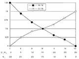
図7は、上述したECRプラズマCVD法によるSiCN系エッチングストッパ膜の成膜において、原料ガスであるC2H4ガス及びN2ガスの混合比を変化させて成膜し、各成膜条件(I〜VII)で形成されたSiCN系膜中のSi原子数に対するC原子数とN原子数の比を調べた結果を示す。ここで、SiCN系膜の形成は、SiH4ガスとC2H4ガスとN2ガスとの混合ガスを用い、流量比をSiH4ガス/(C2H4ガス+N2ガス)=10/30に固定して、C2H4ガスとN2ガスの混合比を変化させて行った。また、膜中のSi、C、Nの各原子数の比は、ラザフォード後方拡散法(Rutherford Backscattering Spectroscopy:RBS)により算出した。
【0040】
図7よりわかるように、形成される膜中のCとNの存在比は、必ずしも用いられるC含有ガスとN含有ガスの混合比とは一致しないが、混合比に従って変化していることがわかる。すなわち、C2H4ガスの混合比を上げれば(N2ガスの混合比を下げれば)、形成される膜中のC原子の存在比が上がり(N原子の存在比が下がり)、この逆とすれば、C原子の存在比は下がる(N原子の存在比は上がる)。ここで、条件Iでは、C2H4ガスを使用しないので、C原子を含まないSiN系膜が形成される。また、条件VIIでは、N2ガスを使用しないので、N原子を含まないSiC系膜が形成される。
【0041】
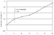
以下では、上記成膜条件(I〜VII)で形成された膜について、エッチング選択比及び金属の拡散性について説明する。
図8は、SiCN系膜のエッチング選択性に関して調べた結果であり、SiN系膜(条件I)のエッチングレートを1としたときの、他の条件下で形成されたSiCN系膜のエッチングレート比を示す。ここで、エッチングは、O2/CF4プラズマガスを用い、下地膜はSiOF膜である。
【0042】
図8よりわかるように、膜中のC含有率が上昇するにつれ、エッチングレート比は増大し、条件VII(SiC系膜)では、条件I(SiN系膜)の2倍弱の値を示している。つまり、膜中のC含有率が高い程選択比が取れ、従って、エッチング形状は良好になる。このように、C原子の数のSi原子の数に対する比(C/Si)が少なくとも0.2以上であれば、良好なエッチング形状が得られる。
【0043】
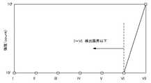
図9は、SiCN系膜の金属拡散性、特に、Cuの拡散性について調べた結果である。Cuは、従来配線として用いられる金属の内で、最も拡散性の高い金属である。具体的には、Si層上に、上記条件(I〜VII)下で成膜された膜500Å(0.05μm)の上にCu層2000Å(0.2μm)を形成し、450℃で7時間熱処理を施した後に、Si/SiCN界面でのCuのSIMS(Secondary Ion Mass Spectroscopy)強度を調べた。一般に、上記条件下で、SIMSによりCuのSi層への拡散が検出されなければデバイス使用上は問題ないとされる。
【0044】
図9よりわかるように、条件I〜VIでは、Si層へのCuの拡散量はSIMSの検出限界以下であり、成膜条件VIIでの膜(SiC系膜)のみにCuの拡散が検出された。このように、膜中にN原子が、少なくともN原子の数のSi原子の数に対する比(N/Si)が0.15以上であるように存在していればCuの拡散が抑えられることがわかる。
【0045】
よって、図7〜図9に示されるように、C/Siが0.2〜0.8であり、かつ、N/Siが0.15〜1.0の組成を有する本実施の形態のSiCN系膜は、低比誘電率(5〜5.5)であるとともに、良好なエッチング選択性及び金属拡散性を備えたエッチングストッパ膜であることがわかる。
【0046】
以上説明したように、本発明によれば、SiとCとNとを主要元素として含有し、信頼性の高い半導体装置及びその製造方法が提供される。詳細には、低誘電率性、下地膜との高いエッチング選択比、及び、低いCu拡散性を有する、ダマシン法に適したエッチングストッパ膜を備えた半導体装置及びその製造方法が提供される。
【0047】
本発明は、上記の実施の形態に限られず、種々の変形、応用が可能である。以下、本発明に適用可能な上記の実施の形態の変形態様について、説明する。
【0048】
上記実施の形態では、エッチングストッパ膜であるSiCN系膜は、ECRプラズマCVDにより成膜した。が、成膜方法はこれに限られず、誘導結合型(Inductive Coupled Plasma:ICP)、ヘリコン(Helicon)型、平行平板型等のプラズマCVDであってもよい。
【0049】
上記実施の形態では、配線を構成する導体層はCuから構成されるとしたが、Cuに限らず、Al或いはAl含有合金等であってもよい。
【0050】
上記実施の形態では、下地膜のエッチングガスとしてO2/CF4ガスを用いるものとした。しかしながら、O2/CF4ガスの代わりにH2ガスとArガスとN2ガスとの混合ガスなどのプラズマを用いることも可能である。また、CF4ガスは、CmFn(m、nは0以上の整数)のクロロカーボン系のガスを使用することができる。
【0051】
上記実施の形態では、エッチングストッパ膜111、SiOF膜112、パッシベーション膜113の、ECRプラズマCVD法による成膜は同一のチャンバ内で行った。しかし、これに限られず、エッチングストッパ膜111を1つのチャンバ内で形成し、SiOF膜112とパッシベーション膜113を別のチャンバ内で形成する、或いは、全ての成膜を個別のチャンバで行い、さらに、別々のプラズマ処理方法を用いるものとしてもよい。しかし、一般に、半導体材料は酸化又は水分吸着し易いので、高真空かつ清浄空気条件下の同一のチャンバ内で全ての処理を行うことが好ましい。
【0052】
上記実施の形態では、SiCN系膜は、SiH4とC2H4とN2を原料ガス化合物として形成した。しかし、原料化合物としては、Si、C、Nを含む化合物であって、単体で、又は、これらを適当に組み合わせた反応によりSiCN系膜が形成されるものならいかなるものでもよい。
【0053】
例えば、本実施の形態のように、Si、C、Nをそれぞれ含む3種の原料ガス化合物を用いる場合には、Si含有化合物としてSiH4を、C含有化合物としてC2H4、CH4、C2H6、C3H8、C2H2等を、N含有化合物としてN2、NF3、N2O、N2O4、NO、N3H8等を適当に組み合わせればよい。
【0054】
また、Si及びCを含む原料化合物と、Nを含む原料化合物の2種のガスを混合して成膜してもよい。この場合、N含有化合物としては上記したものを用い、Si及びCを含む化合物としてアルキルシラン、アルコキシシラン等の有機シランを用いて、これらを適当に組み合わせればよい。アルキルシランとしては、例えば、メチルシラン(SiH3(CH3))、ジメチルシラン(SiH2(CH3)2)、トリメチルシラン(SiH(CH3)3)、テトラメチルシラン(Si(CH3)4)といったメチル化シランが挙げられ、アルコキシシランとしては、例えば、トリメトキシメチルシラン(Si(CH3)(OCH3)3)といったメトキシ化シランが挙げられる。また、これとは逆に、Si及びNを含む原料ガスとCを含む原料ガスを混合するようしてもよい。この場合、C含有化合物としては、上記のものから選択し、Si及びNを含む化合物としては、例えば、ジシラザン(SiH3−NH−SiH3)を用いて、これらを適当に組み合わせればよい。
【0055】
さらには、Si、C、Nを全て含む化合物を原料ガスとして用いることも可能である。このような化合物としては、シラザン結合(−Si−N−)を有する有機シラザン化合物を用いることができる。有機シラザン化合物を用いる場合、例えば、プラズマCVD法により熱重合させて成膜することができる。使用可能な有機シラザン化合物としては、例えば、トリエチルシラザン(SiEt3NH2)、トリプロピルシラザン(SiPr3NH2)、トリフェニルシラザン(SiPh3NH2)、テトラメチルジシラザン(SiMe2H−NH−SiMe2H)、ヘキサメチルジシラザン(SiMe3−NH−SiMe3)、ヘキサエチルジシラザン(SiEt3−NH−SiEt3)、ヘキサフェニルジシラザン(SiPh3−NH−SiPh3)、ヘプタメチルジシラザン(SiMe3−NMe−SiMe3)、ジプロピル−テトラメチルジシラザン(SiPrMe2−NH−SiPrMe2)、ジ−n−ブチル−テトラメチルジシラザン(SiBuMe2−NH−SiBuMe2)、ジ−n−オクチル−テトラメチルジシラザン(SiOcMe2−NH−SiOcMe2)、トリエチル−トリメチルシクロトリシラザン((SiEtH−NMe)3)、ヘキサメチルシクロトリシラザン((SiMe2−NH)3)、ヘキサエチルシクロトリシラザン((SiEt2−NH)3)、ヘキサフェニルシクロトリシラザン((SiPh2−NH)3)、オクタメチルシクロテトラシラザン((SiMe2−NH)4)、オクタエチルシクロテトラシラザン((SiEt2−NH)4)、テトラエチル−テトラメチルシクロテトラシラザン((SiHEt−NMe)4)、シアノプロピルメチルシクロシラザン(SiMeNC(CH2)3−NH)、テトラフェニルジメチルジシラザン(SiMePh2−NH−SiMePh2)、ジフェニル−テトラメチルジシラザン((SiMe2Ph)2−NH)、トリビニル−トリメチルシクロトリシラザン((CH2=CH−SiMe−NH)3)、テトラビニル−テトラメチルシクロテトラシラザン(CH2=CH−SiMe−NH)4、ジビニル−テトラメチルジシラザン(CH2=CH−SiMe2−NH−SiMe2−CH=CH2)が挙げられる。上記式中、Meはメチル基(CH3)、Etはエチル基(C2H5)、Prはプロピル基(C3H7)、Ocはn−オクチル基(n−C8H17)、Phはフェニル基(C6H5)を示す。
【0056】
また、上記の例では、Si、C、Nを含む原料ガスが各1種類あればよいものとしたが、これに限らず、例えば、有機シランとN2の他にC2H2を加えたガスや、有機シラザンの他にN2を加えたガスを用いてもよい。
【0057】
上記実施の形態では、SiOF等からなる1層の層間絶縁膜上にSi、C、Nからなるエッチングストッパ膜を形成し、このエッチングストッパ膜をマスクとしてビアホール及びトレンチホールを形成した。しかし、本実施の形態のエッチングストッパ膜を用いた配線層の形成工程は上記工程に限られない。例えば、ダマシン法の、図11(a)〜(d)に示す工程を2回用いて、ビアホール、トレンチホールを順に形成して、図10に示す構成としてもよい。この場合、まず、上述したSi、C、Nを主要元素として含むビアホール形成用エッチングストッパ膜502をマスクとして用い、下層絶縁層501を選択的にエッチングしてビアホール504を形成する。続いて、上層絶縁層503を形成し、レジスト膜等をマスクとしたエッチングによりトレンチホール505を形成する。
【0058】
上記したような、絶縁層501、503の間にエッチングストッパ膜502を挟み込むような構成として配線層を形成することにより、トレンチホールを所定の深さにエッチングする際に問題となる、トレンチホール505の底部が平坦とならない、或いは、被処理ウェハの中心部と端部に形成されるトレンチホール505の深さが異なる、等のエッチング形状のばらつきを抑えることができる。また、図10に示す構成においても、上記実施の形態に示したように、Si、C、Nを主要元素として含むエッチングストッパ膜は、低い比誘電率を有するので絶縁膜として十分に機能する。
【0059】
【発明の効果】
以上説明したように、本発明によれば、信頼性の高い半導体装置及び半導体装置の製造方法が提供される。より詳細には、低誘電率性、下地膜との高いエッチング選択比、及び、低金属拡散性を有するエッチングストッパ膜を備えた半導体装置及びその製造方法が提供される。
【図面の簡単な説明】
【図1】本発明の実施の形態にかかる半導体装置の部分断面図である。
【図2】本発明の実施の形態にかかる半導体装置の製造工程を順に示す図である。
【図3】本発明の実施の形態にかかる半導体装置の製造工程を順に示す図である。
【図4】本発明の実施の形態にかかる半導体装置の製造工程を順に示す図である。
【図5】本発明の実施の形態にかかる半導体装置の製造工程を順に示す図である。
【図6】本発明の実施の形態にかかる半導体装置の製造工程を順に示す図である。
【図7】C、Nの含有比を変えて形成したSiCN系膜の組成を示す図である。
【図8】図7に示すCN組成を有するSiCN系膜の、SiN系膜のエッチングレートを1とした場合のエッチングレート比を示す図である。
【図9】図7に示すCN組成を有するSiCN系膜のCu拡散性について、SIMS強度について調べた結果を示す図である。
【図10】本発明の他の実施の形態にかかる半導体装置の部分断面図である。
【図11】ダマシン法による配線層の形成工程を順に示す図である。
【符号の説明】
101 第1の下地膜
102 第1の導体層
102a 第1のバリアメタル膜
103 第1のトレンチホール
104 第1のビアホール
105 第1のエッチングストッパ膜
106 第2の下地膜
107 第2の導体層
107a 第2のバリアメタル膜
108 第2のトレンチホール
109 第2のビアホール
110 第2のエッチングストッパ膜
111 第3のエッチングストッパ膜
112 第3の下地膜
113 パッシベーション膜
201 第1のレジスト膜
202 第2のレジスト膜[0001]
BACKGROUND OF THE INVENTION
The present invention relates to a semiconductor device and a method for manufacturing the semiconductor device.
[0002]
[Prior art]
In order to improve the performance of semiconductor integrated circuits, the speed of wiring has been increased. In order to increase the wiring speed, it is effective to reduce the dielectric constant of the interlayer insulating film and reduce the wiring resistance. As an interlayer insulating film having a low dielectric constant, a SiOF film (about 3.5) is used as a
[0003]
When Cu wiring is used, processing by a conventional etching process is difficult, and so-called damascene method is used as a method for realizing Cu multilayer wiring without etching Cu. Hereinafter, the damascene method will be described with reference to FIGS.
[0004]
First, an interlayer insulating film (base film) 602 made of, for example, SiOF and an
[0005]
[Problems to be solved by the invention]
In the above-described damascene method, an etching stopper film is used, and this etching stopper film functions as a mask in etching the base film. Accordingly, a high etching selectivity with respect to the base film is required. In addition, since the etching stopper film also functions as an interlayer insulating film in the semiconductor device, a low relative dielectric constant and a low metal diffusibility are required particularly when the wiring metal is Cu.
[0006]
As such an etching stopper film, a film composed of Si and N as main elements (hereinafter referred to as SiN film) and a film composed of Si and C as main elements (hereinafter referred to as SiC film) are known. Yes. However, the relative dielectric constant of the SiN film is as high as 7-8. In addition, when the underlying film is a fluorine-containing film such as SiOF, and this is plasma etched, the SiN-based film is damaged by fluorine radicals generated during etching, and the etching selectivity cannot be sufficiently obtained, and the processing accuracy Deteriorates. Also, SiC-based films (especially CHn The film containing a group has a good etching selectivity and a relative dielectric constant of around 5 but has a high Cu diffusibility. As described above, the conventional etching stopper film does not sufficiently satisfy the conditions necessary for forming the wiring structure by the damascene method.
[0007]
Accordingly, an object of the present invention is to provide a highly reliable semiconductor device and a manufacturing method thereof.
[0008]
[Means for Solving the Problems]
In order to achieve the above object, a semiconductor device according to a first aspect of the present invention is formed on a first dielectric layer having a low dielectric constant having a plurality of grooves or holes, and the first dielectric layer, A plurality of openings formed to have a plurality of openings that overlap with the plurality of grooves or holes, the second insulating layer containing Si, C, and N as main elements, and the plurality of grooves or holes and the plurality of openings. A conductor layer embedded in a wiring groove or hole ofThe first insulating layer is made of silicon fluoride oxide or carbon fluoride, It is characterized by that.
[0009]
According to the above configuration, the second insulating layer made of Si, C, and N has a dielectric equivalent to or lower than that of a conventional etching stopper film made of Si and C or Si and N. And a good etching selectivity with respect to the first insulating film as compared with these etching stopper films. For this reason, a highly reliable semiconductor device is provided.
[0010]
In the above configuration, in the second insulating layer, the ratio of the number of C atoms to the number of Si atoms is 0.2 to 0.8, and the ratio of the number of N atoms to the number of Si atoms is 0.00. It is preferable that it is 15-1.0. When the abundance ratio of Si, C, and N in the SiCN-based film is in the above range, the etching selectivity of the SiCN film to the first insulating layer is high, and the Cu diffusibility is also reduced.
[0011]
In the above structure, the first insulating layer is made of silicon fluoride oxide or carbon fluoride.Ru . These fluorine-containing films are accompanied by generation of fluorine radicals and the like during plasma etching. However, the SiCN-based second insulating layer (etching stopper film) is resistant to these radicals and has a sufficient etching selectivity with respect to the first insulating layer.
[0012]
The said structure WHEREIN: The said conductor layer may be comprised from Cu. That is, since the second insulating layer composed of Si, C, and N has low Cu diffusibility, a highly reliable wiring layer using Cu is formed.
[0013]
In the above configuration, it is preferable that a barrier metal layer is formed in the wiring groove or hole, and the conductor layer is formed on the barrier metal layer. With this configuration, not only the diffusion of the metal constituting the conductor layer can be suppressed, but also the adhesion between the conductor layer and the interlayer insulating layer can be improved, and the reliability of the semiconductor device can be improved.
[0014]
In the above-described configuration, it is further formed on the second insulating layer and the conductor layer.Si, C, and N are the main elements contained A third insulating layer is preferably provided. Thereby, the spreading | diffusion of the metal from conductor layers, such as Cu, can be suppressed.
[0015]
In order to achieve the above object, a method of manufacturing a semiconductor device according to a second aspect of the present invention includes a step of forming a first insulating layer, and Si, C, and N on the first insulating layer. A step of forming a second insulating layer as a main contained element, and a step of selectively etching the second insulating layer so as to partially expose the surface of the first insulating layer to form an opening. Etching the first insulating layer using the selectively etched second insulating layer as a mask to form a wiring groove or hole, and filling the opening and the wiring groove or hole with a conductor. Forming a layer, and polishing the conductor layer using the second insulating layer as a stopper.The first insulating layer is made of silicon fluoride oxide or carbon fluoride, It is characterized by that.
[0016]
According to the above configuration, the second insulating layer made of Si, C, and N has a dielectric equivalent to or lower than that of a conventional etching stopper film made of Si and C or Si and N. And a favorable etching selectivity with respect to the first insulating layer which is a general interlayer insulating film as compared with these etching stopper films. For this reason, a highly reliable semiconductor device can be manufactured.
[0017]
In the above configuration, in the second insulating layer, the ratio of the number of C atoms to the number of Si atoms is 0.2 to 0.8, and the ratio of the number of N atoms to the number of Si atoms is 0.00. It is preferable that it is 15-1.0. When the abundance ratio of Si, C, and N in the SiCN-based film is in the above range, the etching selectivity of the SiCN film to the base film is high, and the Cu diffusibility is also reduced.
[0018]
In the above structure, the first insulating layer is made of silicon fluoride oxide or carbon fluoride.Ru . These fluorine-containing films are accompanied by generation of fluorine radicals and the like during plasma etching. However, the SiCN-based second insulating layer (etching stopper film) is resistant to these radicals and has a sufficient etching selectivity with respect to the first insulating layer.
[0019]
The said structure WHEREIN: The said conductor layer may be comprised from Cu. That is, since the second insulating layer composed of Si, C, and N has low Cu diffusibility, a highly reliable wiring layer using Cu is formed.
[0020]
The said structure WHEREIN: It is preferable to further provide the process of forming a barrier metal layer between the said conductor layer, the said opening, and the said wiring groove | channel or a hole. With this configuration, not only the diffusion of the metal constituting the conductor layer can be suppressed, but also the adhesion between the conductor layer and the interlayer insulating layer can be improved, and the reliability of the semiconductor device can be improved.
[0021]
In the above configuration, further, on the second insulating layer and the conductor layer,Si, C, and N are the main contained elements It is preferable to include a step of forming a third insulating layer. Thereby, the spreading | diffusion of the metal from conductor layers, such as Cu, can be suppressed.
[0022]
DETAILED DESCRIPTION OF THE INVENTION
A semiconductor device according to an embodiment of the present invention will be described below with reference to the drawings.
FIG. 1 is a partial cross-sectional view showing the configuration of the semiconductor device of the present embodiment. In this semiconductor device, a multilayer wiring layer is formed on an insulating film (not shown) covering an element such as a MOS transistor formed on a substrate such as Si. FIG. 1 is formed on the surface of the substrate. The wiring layer is shown.
[0023]
As shown in FIG. 1, a lower layer wiring composed of a first base film (interlayer insulating film) 101, a
[0024]
The
[0025]
The first
[0026]
A
[0027]
A third etching stopper film 111 is formed on the uppermost wiring layer HL, which is the same as the first and second etching stopper films configured with Si, C, and N as main elements. It has a structure and has a function of suppressing diffusion of metal from a conductor layer made of Cu or the like. Further, on the third etching stopper film 111, a
[0028]
Next, a method for manufacturing the semiconductor device described above will be described. In the present embodiment, a semiconductor device is manufactured using a dual damascene method that forms a trench hole and a via hole, which is a modification of the damascene method.
[0029]
2 to 6 are diagrams sequentially illustrating a Cu wiring forming process by a dual damascene method. Hereinafter, description will be made sequentially with reference to the drawings.
[0030]
First, as shown in FIG. 2A, a second base film is formed on a lower wiring layer LL including a
[0031]
The second
[0032]
Next, as shown in FIG. 2B, a first resist
[0033]
Subsequently, as shown in FIG. 3A, for example, CF is used with the first resist
[0034]
Next, as shown in FIG. 3A, anisotropic etching is performed using the second
[0035]
Subsequently, as shown in FIG. 4A, a second resist
[0036]
Next, as shown in FIG. 4B, the
[0037]
Subsequently, as shown in FIG. 5A, a second
[0038]
Finally, as shown in FIG. 6, a third etching stopper film 111 is formed on the substrate surface under the same film formation conditions as the second
[0039]
Here, the SiCN-based film used as the etching mask for the
FIG. 7 shows the source gas C in the formation of the SiCN-based etching stopper film by the ECR plasma CVD method described above.2 H4 Gas and N2 The result of examining the ratio of the number of C atoms and the number of N atoms with respect to the number of Si atoms in the SiCN-based film formed under various film formation conditions (I to VII) is shown. Here, the formation of the SiCN film is SiH.4 Gas and C2 H4 Gas and N2 Using a mixed gas with the gas, the flow rate ratio is SiH4 Gas / (C2 H4 Gas + N2 Gas) = 10/30, C2 H4 Gas and N2 This was done by changing the gas mixing ratio. The ratio of the number of Si, C, and N atoms in the film was calculated by Rutherford Backscattering Spectroscopy (RBS).
[0040]
As can be seen from FIG. 7, the abundance ratio of C and N in the formed film does not necessarily match the mixing ratio of the C-containing gas and N-containing gas used, but changes according to the mixing ratio. . That is, C2 H4 If the gas mixing ratio is increased (N2 If the gas mixing ratio is lowered), the abundance ratio of C atoms in the formed film increases (the abundance ratio of N atoms decreases), and vice versa, the abundance ratio of C atoms decreases (the presence of N atoms). Ratio goes up). Here, in condition I, C2 H4 Since no gas is used, a SiN-based film containing no C atoms is formed. In condition VII, N2 Since no gas is used, an SiC-based film containing no N atoms is formed.
[0041]
Hereinafter, the etching selectivity and the metal diffusibility of the film formed under the film forming conditions (I to VII) will be described.
FIG. 8 shows the results of investigation on the etching selectivity of the SiCN-based film. When the etching rate of the SiN-based film (condition I) is 1, the etching rate ratio of the SiCN-based film formed under other conditions is shown. Indicates. Here, the etching is O2 / CF4 A plasma gas is used, and the base film is a SiOF film.
[0042]
As can be seen from FIG. 8, as the C content in the film increases, the etching rate ratio increases. Under the condition VII (SiC film), the value is slightly less than twice that of the condition I (SiN film). Yes. That is, the higher the C content in the film, the higher the selectivity, and the better the etching shape. Thus, if the ratio of the number of C atoms to the number of Si atoms (C / Si) is at least 0.2 or more, a good etching shape can be obtained.
[0043]
FIG. 9 shows the results of examining the metal diffusibility of the SiCN-based film, particularly the Cu diffusivity. Cu is a metal having the highest diffusibility among metals conventionally used as wiring. Specifically, on the Si layer, a Cu layer 2000 mm (0.2 μm) is formed on a film 500 mm (0.05 μm) formed under the above conditions (I to VII), and the temperature is 450 ° C. for 7 hours. After the heat treatment, the SIMS (Secondary Ion Mass Spectroscopy) strength of Cu at the Si / SiCN interface was examined. In general, if diffusion of Cu into the Si layer is not detected by SIMS under the above conditions, there is no problem in using the device.
[0044]
As can be seen from FIG. 9, under conditions I to VI, the amount of Cu diffusion into the Si layer is below the SIMS detection limit, and Cu diffusion is detected only in the film (SiC film) under the film formation condition VII. It was. Thus, if N atoms exist in the film so that at least the ratio of N atoms to the number of Si atoms (N / Si) is 0.15 or more, the diffusion of Cu can be suppressed. Recognize.
[0045]
Accordingly, as shown in FIGS. 7 to 9, the SiCN of the present embodiment having a composition in which C / Si is 0.2 to 0.8 and N / Si is 0.15 to 1.0. It can be seen that the system film is an etching stopper film having a low relative dielectric constant (5 to 5.5) and good etching selectivity and metal diffusibility.
[0046]
As described above, according to the present invention, a highly reliable semiconductor device containing Si, C, and N as main elements and a method for manufacturing the same are provided. Specifically, there are provided a semiconductor device having an etching stopper film suitable for the damascene method, having a low dielectric constant, a high etching selectivity with a base film, and a low Cu diffusivity, and a method for manufacturing the same.
[0047]
The present invention is not limited to the above-described embodiment, and various modifications and applications are possible. Hereinafter, modifications of the above-described embodiment applicable to the present invention will be described.
[0048]
In the above embodiment, the SiCN-based film that is the etching stopper film is formed by ECR plasma CVD. However, the film forming method is not limited to this, and plasma CVD such as inductive coupled plasma (ICP), helicon type, and parallel plate type may be used.
[0049]
In the above embodiment, the conductor layer constituting the wiring is made of Cu. However, the conductor layer is not limited to Cu, and may be Al or an Al-containing alloy.
[0050]
In the above embodiment,
[0051]
In the above embodiment, the etching stopper film 111, the
[0052]
In the above embodiment, the SiCN-based film is SiH.4 And C2 H4 And N2 Was formed as a raw material gas compound. However, the raw material compound may be any compound containing Si, C, and N as long as the SiCN-based film can be formed by itself or by a reaction in which these are appropriately combined.
[0053]
For example, as in the present embodiment, when three source gas compounds each containing Si, C, and N are used, SiH is used as the Si-containing compound.4 C as a C-containing compound2 H4 , CH4 , C2 H6 , C3 H8 , C2 H2 Etc. as N-containing compounds2 , NF3 , N2 O, N2 O4 , NO, N3 H8 Etc. may be combined appropriately.
[0054]
Alternatively, a film may be formed by mixing two kinds of gases, a raw material compound containing Si and C, and a raw material compound containing N. In this case, the above-described compounds may be used as the N-containing compound, and organic silanes such as alkylsilanes and alkoxysilanes may be used as the compounds containing Si and C, and these may be combined appropriately. Examples of the alkyl silane include methyl silane (SiH3 (CH3 )), Dimethylsilane (SiH)2 (CH3 )2 ), Trimethylsilane (SiH (CH3 )3 ), Tetramethylsilane (Si (CH3 )4 ), And as the alkoxysilane, for example, trimethoxymethylsilane (Si (CH3 ) (OCH3 )3 And methoxylated silanes. On the contrary, a source gas containing Si and N and a source gas containing C may be mixed. In this case, the C-containing compound is selected from the above, and the compound containing Si and N is, for example, disilazane (SiH3 -NH-SiH3 ) To combine these appropriately.
[0055]
Furthermore, a compound containing all of Si, C, and N can be used as a source gas. As such a compound, an organic silazane compound having a silazane bond (—Si—N—) can be used. In the case of using an organic silazane compound, for example, the film can be formed by thermal polymerization by a plasma CVD method. Examples of usable organic silazane compounds include triethylsilazane (SiEt).3 NH2 ), Tripropylsilazane (SiPr)3 NH2 ), Triphenylsilazane (SiPh)3 NH2 ), Tetramethyldisilazane (SiMe)2 H-NH-SiMe2 H), hexamethyldisilazane (SiMe)3 -NH-SiMe3 ), Hexaethyldisilazane (SiEt)3 -NH-SiEt3 ), Hexaphenyldisilazane (SiPh)3 -NH-SiPh3 ), Heptamethyldisilazane (SiMe)3 -NMe-SiMe3 ), Dipropyl-tetramethyldisilazane (SiPrMe)2 -NH-SiPrMe2 ), Di-n-butyl-tetramethyldisilazane (SiBuMe)2 -NH-SiBuMe2 ), Di-n-octyl-tetramethyldisilazane (SiOcMe)2 -NH-SiOcMe2 ), Triethyl-trimethylcyclotrisilazane ((SiEtH-NMe))3 ), Hexamethylcyclotrisilazane ((SiMe2 -NH)3 ), Hexaethylcyclotrisilazane ((SiEt2 -NH)3 ), Hexaphenylcyclotrisilazane ((SiPh2 -NH)3 ), Octamethylcyclotetrasilazane ((SiMe2 -NH)4 ), Octaethylcyclotetrasilazane ((SiEt2 -NH)4 ), Tetraethyl-tetramethylcyclotetrasilazane ((SiHEt-NMe))4 ), Cyanopropylmethylcyclosilazane (SiMeNC (CH2 )3 -NH), tetraphenyldimethyldisilazane (SiMePh)2 -NH-SiMePh2 ), Diphenyl-tetramethyldisilazane ((SiMe2 Ph)2 -NH), trivinyl-trimethylcyclotrisilazane ((CH2 = CH-SiMe-NH)3 ), Tetravinyl-tetramethylcyclotetrasilazane (CH2 = CH-SiMe-NH)4 , Divinyl-tetramethyldisilazane (CH2 = CH-SiMe2 -NH-SiMe2 -CH = CH2 ). In the above formula, Me represents a methyl group (CH3 ), Et is an ethyl group (C2 H5 ), Pr is a propyl group (C3 H7 ), Oc is an n-octyl group (n-C8 H17 ), Ph is a phenyl group (C6 H5 ).
[0056]
In the above example, only one source gas containing Si, C, and N is required. However, the present invention is not limited to this. For example, organic silane and N2 In addition to C2 H2 N in addition to the gas added with organic silazane2 A gas added with may be used.
[0057]
In the above embodiment, an etching stopper film made of Si, C, and N is formed on a single interlayer insulating film made of SiOF or the like, and a via hole and a trench hole are formed using this etching stopper film as a mask. However, the formation process of the wiring layer using the etching stopper film of the present embodiment is not limited to the above process. For example, by using the damascene method shown in FIGS. 11A to 11D twice, a via hole and a trench hole may be formed in order, and the configuration shown in FIG. In this case, first, the via
[0058]
By forming the wiring layer in such a structure that the
[0059]
【The invention's effect】
As described above, according to the present invention, a highly reliable semiconductor device and a method for manufacturing the semiconductor device are provided. More specifically, a semiconductor device including an etching stopper film having low dielectric constant, high etching selectivity with a base film, and low metal diffusibility, and a method for manufacturing the same are provided.
[Brief description of the drawings]
FIG. 1 is a partial cross-sectional view of a semiconductor device according to an embodiment of the present invention.
FIG. 2 is a diagram sequentially illustrating a manufacturing process of the semiconductor device according to the embodiment of the present invention.
FIGS. 3A and 3B are diagrams sequentially illustrating a manufacturing process of the semiconductor device according to the embodiment of the invention. FIGS.
FIGS. 4A and 4B are diagrams sequentially illustrating a manufacturing process of the semiconductor device according to the embodiment of the invention. FIGS.
FIGS. 5A and 5B are diagrams sequentially illustrating a manufacturing process of the semiconductor device according to the embodiment of the invention. FIGS.
FIGS. 6A and 6B are diagrams sequentially illustrating a manufacturing process of the semiconductor device according to the embodiment of the invention. FIGS.
FIG. 7 is a diagram showing the composition of a SiCN-based film formed by changing the content ratio of C and N.
8 is a diagram showing an etching rate ratio of the SiCN-based film having the CN composition shown in FIG. 7 when the SiN-based film has an etching rate of 1. FIG.
9 is a diagram showing the results of investigating SIMS intensity for Cu diffusivity of the SiCN-based film having the CN composition shown in FIG. 7; FIG.
FIG. 10 is a partial cross-sectional view of a semiconductor device according to another embodiment of the present invention.
FIGS. 11A and 11B are diagrams sequentially illustrating a wiring layer forming process by a damascene method. FIGS.
[Explanation of symbols]
101 First undercoat film
102 1st conductor layer
102a First barrier metal film
103 First trench hole
104 First via hole
105 First etching stopper film
106 Second underlayer
107 second conductor layer
107a Second barrier metal film
108 Second trench hole
109 Second via hole
110 Second etching stopper film
111 Third etching stopper film
112 Third underlayer
113 Passivation film
201 First resist film
202 Second resist film
Claims (10)
Translated fromJapanese前記第1の絶縁層上に形成され、前記複数の溝又は穴と重なる複数の開口を有し、SiとCとNとを主たる含有元素とする第2の絶縁層と、
前記複数の溝又は穴と前記複数の開口とから形成される複数の配線溝又は穴に埋め込まれた導体層と、
を備え、
前記第1の絶縁層は、フッ化酸化ケイ素又はフッ化カーボンから構成される、
ことを特徴とする半導体装置。A low dielectric constant first insulating layer having a plurality of grooves or holes;
A second insulating layer formed on the first insulating layer, having a plurality of openings overlapping the plurality of grooves or holes, and containing Si, C, and N as main elements;
A conductor layer embedded in a plurality of wiring grooves or holes formed from the plurality of grooves or holes and the plurality of openings;
Equipped witha,
The first insulating layer is composed of silicon fluoride oxide or carbon fluoride,
A semiconductor device.
前記第1の絶縁層上に、SiとCとNとを主たる含有元素とする第2の絶縁層を形成する工程と、
前記第1の絶縁層の表面が部分的に露出するよう、前記第2の絶縁層を選択的にエッチングして開口を形成する工程と、
前記選択的にエッチングされた第2の絶縁層をマスクとして前記第1の絶縁層をエッチングして、配線溝又は穴を形成する工程と、
前記開口及び前記配線溝又は穴を埋めて導体層を形成する工程と、
前記導体層を、前記第2の絶縁層をストッパとして研磨する工程と、
を備え、
前記第1の絶縁層は、フッ化酸化ケイ素又はフッ化カーボンから構成される、
ことを特徴とする半導体装置の製造方法。Forming a first insulating layer;
Forming a second insulating layer containing Si, C, and N as main elements on the first insulating layer;
Selectively etching the second insulating layer to form an opening so that the surface of the first insulating layer is partially exposed;
Etching the first insulating layer using the selectively etched second insulating layer as a mask to form a wiring groove or hole;
Forming a conductor layer by filling the opening and the wiring groove or hole;
Polishing the conductor layer using the second insulating layer as a stopper;
Equipped witha,
The first insulating layer is composed of silicon fluoride oxide or carbon fluoride,
A method for manufacturing a semiconductor device.
Priority Applications (7)
| Application Number | Priority Date | Filing Date | Title |
|---|---|---|---|
| JP2000274426AJP4484345B2 (en) | 2000-09-11 | 2000-09-11 | Semiconductor device and manufacturing method thereof |
| EP01965571AEP1320884A2 (en) | 2000-09-11 | 2001-09-11 | Semiconductor device and fabrication method therefor |
| PCT/JP2001/007880WO2002023625A2 (en) | 2000-09-11 | 2001-09-11 | Semiconductor device and fabrication method therefor |
| TW090122485ATW530380B (en) | 2000-09-11 | 2001-09-11 | Semiconductor device and fabrication method therefor |
| KR10-2003-7003543AKR100479796B1 (en) | 2000-09-11 | 2001-09-11 | Semiconductor device and fabrication method therefor |
| US10/380,038US6949829B2 (en) | 2000-09-11 | 2001-09-11 | Semiconductor device and fabrication method therefor |
| EP07001638AEP1777739A3 (en) | 2000-09-11 | 2001-09-11 | Semiconductor device and fabrication method therefor |
Applications Claiming Priority (1)
| Application Number | Priority Date | Filing Date | Title |
|---|---|---|---|
| JP2000274426AJP4484345B2 (en) | 2000-09-11 | 2000-09-11 | Semiconductor device and manufacturing method thereof |
Publications (2)
| Publication Number | Publication Date |
|---|---|
| JP2002083869A JP2002083869A (en) | 2002-03-22 |
| JP4484345B2true JP4484345B2 (en) | 2010-06-16 |
Family
ID=18760186
Family Applications (1)
| Application Number | Title | Priority Date | Filing Date |
|---|---|---|---|
| JP2000274426AExpired - Fee RelatedJP4484345B2 (en) | 2000-09-11 | 2000-09-11 | Semiconductor device and manufacturing method thereof |
Country Status (1)
| Country | Link |
|---|---|
| JP (1) | JP4484345B2 (en) |
Families Citing this family (92)
| Publication number | Priority date | Publication date | Assignee | Title |
|---|---|---|---|---|
| JP4086673B2 (en) | 2003-02-04 | 2008-05-14 | Necエレクトロニクス株式会社 | Semiconductor device and manufacturing method thereof |
| US7803705B2 (en)* | 2004-01-13 | 2010-09-28 | Tokyo Electron Limited | Manufacturing method of semiconductor device and film deposition system |
| JP4202951B2 (en) | 2004-03-08 | 2008-12-24 | 東京エレクトロン株式会社 | Wiring formation method for semiconductor device |
| JP5019741B2 (en) | 2005-11-30 | 2012-09-05 | 東京エレクトロン株式会社 | Semiconductor device manufacturing method and substrate processing system |
| JP5261291B2 (en) | 2009-06-01 | 2013-08-14 | 東京エレクトロン株式会社 | Processing method and storage medium |
| US10283321B2 (en) | 2011-01-18 | 2019-05-07 | Applied Materials, Inc. | Semiconductor processing system and methods using capacitively coupled plasma |
| US9064815B2 (en) | 2011-03-14 | 2015-06-23 | Applied Materials, Inc. | Methods for etch of metal and metal-oxide films |
| JP5941623B2 (en) | 2011-03-25 | 2016-06-29 | 東京エレクトロン株式会社 | Processing method and storage medium |
| US9267739B2 (en) | 2012-07-18 | 2016-02-23 | Applied Materials, Inc. | Pedestal with multi-zone temperature control and multiple purge capabilities |
| US9373517B2 (en) | 2012-08-02 | 2016-06-21 | Applied Materials, Inc. | Semiconductor processing with DC assisted RF power for improved control |
| US9390937B2 (en)* | 2012-09-20 | 2016-07-12 | Applied Materials, Inc. | Silicon-carbon-nitride selective etch |
| US9132436B2 (en) | 2012-09-21 | 2015-09-15 | Applied Materials, Inc. | Chemical control features in wafer process equipment |
| US10256079B2 (en) | 2013-02-08 | 2019-04-09 | Applied Materials, Inc. | Semiconductor processing systems having multiple plasma configurations |
| US9362130B2 (en) | 2013-03-01 | 2016-06-07 | Applied Materials, Inc. | Enhanced etching processes using remote plasma sources |
| US9418889B2 (en)* | 2014-06-30 | 2016-08-16 | Lam Research Corporation | Selective formation of dielectric barriers for metal interconnects in semiconductor devices |
| JP6315694B2 (en) | 2014-09-19 | 2018-04-25 | 東京エレクトロン株式会社 | Semiconductor device manufacturing method, and film forming method and forming apparatus |
| US9355922B2 (en) | 2014-10-14 | 2016-05-31 | Applied Materials, Inc. | Systems and methods for internal surface conditioning in plasma processing equipment |
| US9966240B2 (en) | 2014-10-14 | 2018-05-08 | Applied Materials, Inc. | Systems and methods for internal surface conditioning assessment in plasma processing equipment |
| US11637002B2 (en) | 2014-11-26 | 2023-04-25 | Applied Materials, Inc. | Methods and systems to enhance process uniformity |
| US10573496B2 (en) | 2014-12-09 | 2020-02-25 | Applied Materials, Inc. | Direct outlet toroidal plasma source |
| US10224210B2 (en) | 2014-12-09 | 2019-03-05 | Applied Materials, Inc. | Plasma processing system with direct outlet toroidal plasma source |
| US11257693B2 (en) | 2015-01-09 | 2022-02-22 | Applied Materials, Inc. | Methods and systems to improve pedestal temperature control |
| US20160225652A1 (en) | 2015-02-03 | 2016-08-04 | Applied Materials, Inc. | Low temperature chuck for plasma processing systems |
| US9728437B2 (en) | 2015-02-03 | 2017-08-08 | Applied Materials, Inc. | High temperature chuck for plasma processing systems |
| US9881805B2 (en) | 2015-03-02 | 2018-01-30 | Applied Materials, Inc. | Silicon selective removal |
| US9691645B2 (en) | 2015-08-06 | 2017-06-27 | Applied Materials, Inc. | Bolted wafer chuck thermal management systems and methods for wafer processing systems |
| US9741593B2 (en) | 2015-08-06 | 2017-08-22 | Applied Materials, Inc. | Thermal management systems and methods for wafer processing systems |
| US9349605B1 (en) | 2015-08-07 | 2016-05-24 | Applied Materials, Inc. | Oxide etch selectivity systems and methods |
| US10504700B2 (en) | 2015-08-27 | 2019-12-10 | Applied Materials, Inc. | Plasma etching systems and methods with secondary plasma injection |
| US10522371B2 (en) | 2016-05-19 | 2019-12-31 | Applied Materials, Inc. | Systems and methods for improved semiconductor etching and component protection |
| US10504754B2 (en) | 2016-05-19 | 2019-12-10 | Applied Materials, Inc. | Systems and methods for improved semiconductor etching and component protection |
| US9865484B1 (en) | 2016-06-29 | 2018-01-09 | Applied Materials, Inc. | Selective etch using material modification and RF pulsing |
| US10629473B2 (en) | 2016-09-09 | 2020-04-21 | Applied Materials, Inc. | Footing removal for nitride spacer |
| US10062575B2 (en) | 2016-09-09 | 2018-08-28 | Applied Materials, Inc. | Poly directional etch by oxidation |
| US10546729B2 (en) | 2016-10-04 | 2020-01-28 | Applied Materials, Inc. | Dual-channel showerhead with improved profile |
| US10062585B2 (en) | 2016-10-04 | 2018-08-28 | Applied Materials, Inc. | Oxygen compatible plasma source |
| US9934942B1 (en) | 2016-10-04 | 2018-04-03 | Applied Materials, Inc. | Chamber with flow-through source |
| US10062579B2 (en) | 2016-10-07 | 2018-08-28 | Applied Materials, Inc. | Selective SiN lateral recess |
| US9947549B1 (en) | 2016-10-10 | 2018-04-17 | Applied Materials, Inc. | Cobalt-containing material removal |
| US9768034B1 (en) | 2016-11-11 | 2017-09-19 | Applied Materials, Inc. | Removal methods for high aspect ratio structures |
| US10163696B2 (en) | 2016-11-11 | 2018-12-25 | Applied Materials, Inc. | Selective cobalt removal for bottom up gapfill |
| US10242908B2 (en) | 2016-11-14 | 2019-03-26 | Applied Materials, Inc. | Airgap formation with damage-free copper |
| US10026621B2 (en) | 2016-11-14 | 2018-07-17 | Applied Materials, Inc. | SiN spacer profile patterning |
| US10566206B2 (en) | 2016-12-27 | 2020-02-18 | Applied Materials, Inc. | Systems and methods for anisotropic material breakthrough |
| US10431429B2 (en) | 2017-02-03 | 2019-10-01 | Applied Materials, Inc. | Systems and methods for radial and azimuthal control of plasma uniformity |
| US10403507B2 (en) | 2017-02-03 | 2019-09-03 | Applied Materials, Inc. | Shaped etch profile with oxidation |
| US10043684B1 (en) | 2017-02-06 | 2018-08-07 | Applied Materials, Inc. | Self-limiting atomic thermal etching systems and methods |
| US10319739B2 (en) | 2017-02-08 | 2019-06-11 | Applied Materials, Inc. | Accommodating imperfectly aligned memory holes |
| US10943834B2 (en) | 2017-03-13 | 2021-03-09 | Applied Materials, Inc. | Replacement contact process |
| US10319649B2 (en) | 2017-04-11 | 2019-06-11 | Applied Materials, Inc. | Optical emission spectroscopy (OES) for remote plasma monitoring |
| US11276590B2 (en) | 2017-05-17 | 2022-03-15 | Applied Materials, Inc. | Multi-zone semiconductor substrate supports |
| US11276559B2 (en) | 2017-05-17 | 2022-03-15 | Applied Materials, Inc. | Semiconductor processing chamber for multiple precursor flow |
| JP7176860B6 (en) | 2017-05-17 | 2022-12-16 | アプライド マテリアルズ インコーポレイテッド | Semiconductor processing chamber to improve precursor flow |
| US10497579B2 (en) | 2017-05-31 | 2019-12-03 | Applied Materials, Inc. | Water-free etching methods |
| US10049891B1 (en) | 2017-05-31 | 2018-08-14 | Applied Materials, Inc. | Selective in situ cobalt residue removal |
| US10920320B2 (en) | 2017-06-16 | 2021-02-16 | Applied Materials, Inc. | Plasma health determination in semiconductor substrate processing reactors |
| US10541246B2 (en) | 2017-06-26 | 2020-01-21 | Applied Materials, Inc. | 3D flash memory cells which discourage cross-cell electrical tunneling |
| US10727080B2 (en) | 2017-07-07 | 2020-07-28 | Applied Materials, Inc. | Tantalum-containing material removal |
| US10541184B2 (en) | 2017-07-11 | 2020-01-21 | Applied Materials, Inc. | Optical emission spectroscopic techniques for monitoring etching |
| US10354889B2 (en) | 2017-07-17 | 2019-07-16 | Applied Materials, Inc. | Non-halogen etching of silicon-containing materials |
| US10043674B1 (en) | 2017-08-04 | 2018-08-07 | Applied Materials, Inc. | Germanium etching systems and methods |
| US10170336B1 (en) | 2017-08-04 | 2019-01-01 | Applied Materials, Inc. | Methods for anisotropic control of selective silicon removal |
| US10297458B2 (en) | 2017-08-07 | 2019-05-21 | Applied Materials, Inc. | Process window widening using coated parts in plasma etch processes |
| JP2019062142A (en) | 2017-09-28 | 2019-04-18 | 東京エレクトロン株式会社 | Selective film formation method and semiconductor device manufacturing method |
| US10128086B1 (en) | 2017-10-24 | 2018-11-13 | Applied Materials, Inc. | Silicon pretreatment for nitride removal |
| US10283324B1 (en) | 2017-10-24 | 2019-05-07 | Applied Materials, Inc. | Oxygen treatment for nitride etching |
| US10256112B1 (en) | 2017-12-08 | 2019-04-09 | Applied Materials, Inc. | Selective tungsten removal |
| US10903054B2 (en) | 2017-12-19 | 2021-01-26 | Applied Materials, Inc. | Multi-zone gas distribution systems and methods |
| US11328909B2 (en) | 2017-12-22 | 2022-05-10 | Applied Materials, Inc. | Chamber conditioning and removal processes |
| US10854426B2 (en) | 2018-01-08 | 2020-12-01 | Applied Materials, Inc. | Metal recess for semiconductor structures |
| US10964512B2 (en) | 2018-02-15 | 2021-03-30 | Applied Materials, Inc. | Semiconductor processing chamber multistage mixing apparatus and methods |
| US10679870B2 (en) | 2018-02-15 | 2020-06-09 | Applied Materials, Inc. | Semiconductor processing chamber multistage mixing apparatus |
| TWI766433B (en) | 2018-02-28 | 2022-06-01 | 美商應用材料股份有限公司 | Systems and methods to form airgaps |
| US10593560B2 (en) | 2018-03-01 | 2020-03-17 | Applied Materials, Inc. | Magnetic induction plasma source for semiconductor processes and equipment |
| US10319600B1 (en) | 2018-03-12 | 2019-06-11 | Applied Materials, Inc. | Thermal silicon etch |
| US10497573B2 (en) | 2018-03-13 | 2019-12-03 | Applied Materials, Inc. | Selective atomic layer etching of semiconductor materials |
| US10573527B2 (en) | 2018-04-06 | 2020-02-25 | Applied Materials, Inc. | Gas-phase selective etching systems and methods |
| US10490406B2 (en) | 2018-04-10 | 2019-11-26 | Appled Materials, Inc. | Systems and methods for material breakthrough |
| US10699879B2 (en) | 2018-04-17 | 2020-06-30 | Applied Materials, Inc. | Two piece electrode assembly with gap for plasma control |
| US10886137B2 (en) | 2018-04-30 | 2021-01-05 | Applied Materials, Inc. | Selective nitride removal |
| US10872778B2 (en) | 2018-07-06 | 2020-12-22 | Applied Materials, Inc. | Systems and methods utilizing solid-phase etchants |
| US10755941B2 (en) | 2018-07-06 | 2020-08-25 | Applied Materials, Inc. | Self-limiting selective etching systems and methods |
| US10672642B2 (en) | 2018-07-24 | 2020-06-02 | Applied Materials, Inc. | Systems and methods for pedestal configuration |
| US10892198B2 (en) | 2018-09-14 | 2021-01-12 | Applied Materials, Inc. | Systems and methods for improved performance in semiconductor processing |
| US11049755B2 (en) | 2018-09-14 | 2021-06-29 | Applied Materials, Inc. | Semiconductor substrate supports with embedded RF shield |
| US11062887B2 (en) | 2018-09-17 | 2021-07-13 | Applied Materials, Inc. | High temperature RF heater pedestals |
| US11417534B2 (en) | 2018-09-21 | 2022-08-16 | Applied Materials, Inc. | Selective material removal |
| US11682560B2 (en) | 2018-10-11 | 2023-06-20 | Applied Materials, Inc. | Systems and methods for hafnium-containing film removal |
| US11121002B2 (en) | 2018-10-24 | 2021-09-14 | Applied Materials, Inc. | Systems and methods for etching metals and metal derivatives |
| US11437242B2 (en) | 2018-11-27 | 2022-09-06 | Applied Materials, Inc. | Selective removal of silicon-containing materials |
| US11721527B2 (en) | 2019-01-07 | 2023-08-08 | Applied Materials, Inc. | Processing chamber mixing systems |
| US10920319B2 (en) | 2019-01-11 | 2021-02-16 | Applied Materials, Inc. | Ceramic showerheads with conductive electrodes |
- 2000
- 2000-09-11JPJP2000274426Apatent/JP4484345B2/ennot_activeExpired - Fee Related
Also Published As
| Publication number | Publication date |
|---|---|
| JP2002083869A (en) | 2002-03-22 |
Similar Documents
| Publication | Publication Date | Title |
|---|---|---|
| JP4484345B2 (en) | Semiconductor device and manufacturing method thereof | |
| US6949829B2 (en) | Semiconductor device and fabrication method therefor | |
| US7088003B2 (en) | Structures and methods for integration of ultralow-k dielectrics with improved reliability | |
| JP3927771B2 (en) | Method for forming a microelectronic structure | |
| CN101506955B (en) | Dielectric spacers for metal interconnects and methods of forming same | |
| KR102263321B1 (en) | Low-k dielectric and processes for forming same | |
| TW516108B (en) | Dual damascene process using oxide liner as dielectric barrier layer | |
| US7830010B2 (en) | Surface treatment for selective metal cap applications | |
| US7795740B2 (en) | Adhesion enhancement for metal/dielectric interface | |
| US8927442B1 (en) | SiCOH hardmask with graded transition layers | |
| KR100227287B1 (en) | A buried conductive layer and its formation method | |
| JP2000174123A (en) | Semiconductor device and manufacturing method thereof | |
| US20030001282A1 (en) | Metal barrier behavior by sic:h deposition on porous materials | |
| JP5119832B2 (en) | Interface roughness reducing film, wiring layer, semiconductor device, and method of manufacturing semiconductor device | |
| TW200414283A (en) | Semiconductor device and the manufacturing method thereof | |
| CN101017808B (en) | Semiconductor device and manufacturing method thereof | |
| TWI588935B (en) | Method for forming semiconductor device structure | |
| JP2003017496A (en) | Semiconductor device and manufacturing method thereof | |
| JP2002526649A (en) | Method of depositing silicon carbide and use as barrier and passivation layers | |
| JP2003152076A (en) | Semiconductor device and method of manufacturing the same | |
| US9087877B2 (en) | Low-k interconnect structures with reduced RC delay | |
| US20070222076A1 (en) | Single or dual damascene structure reducing or eliminating the formation of micro-trenches arising from lithographic misalignment | |
| JP2002083870A (en) | Semiconductor device and production method therefor | |
| CN1497700A (en) | Semiconductor device and manufacturing method thereof | |
| US6657284B1 (en) | Graded dielectric layer and method for fabrication thereof |
Legal Events
| Date | Code | Title | Description |
|---|---|---|---|
| A621 | Written request for application examination | Free format text:JAPANESE INTERMEDIATE CODE: A621 Effective date:20060301 | |
| A131 | Notification of reasons for refusal | Free format text:JAPANESE INTERMEDIATE CODE: A131 Effective date:20091110 | |
| A521 | Written amendment | Free format text:JAPANESE INTERMEDIATE CODE: A523 Effective date:20100105 | |
| TRDD | Decision of grant or rejection written | ||
| A01 | Written decision to grant a patent or to grant a registration (utility model) | Free format text:JAPANESE INTERMEDIATE CODE: A01 Effective date:20100309 | |
| A01 | Written decision to grant a patent or to grant a registration (utility model) | Free format text:JAPANESE INTERMEDIATE CODE: A01 | |
| A61 | First payment of annual fees (during grant procedure) | Free format text:JAPANESE INTERMEDIATE CODE: A61 Effective date:20100323 | |
| R150 | Certificate of patent or registration of utility model | Ref document number:4484345 Country of ref document:JP Free format text:JAPANESE INTERMEDIATE CODE: R150 Free format text:JAPANESE INTERMEDIATE CODE: R150 | |
| FPAY | Renewal fee payment (event date is renewal date of database) | Free format text:PAYMENT UNTIL: 20130402 Year of fee payment:3 | |
| FPAY | Renewal fee payment (event date is renewal date of database) | Free format text:PAYMENT UNTIL: 20160402 Year of fee payment:6 | |
| R250 | Receipt of annual fees | Free format text:JAPANESE INTERMEDIATE CODE: R250 | |
| R250 | Receipt of annual fees | Free format text:JAPANESE INTERMEDIATE CODE: R250 | |
| LAPS | Cancellation because of no payment of annual fees |