JP4478859B2 - Polishing pad - Google Patents
Polishing padDownload PDFInfo
- Publication number
- JP4478859B2 JP4478859B2JP2003117776AJP2003117776AJP4478859B2JP 4478859 B2JP4478859 B2JP 4478859B2JP 2003117776 AJP2003117776 AJP 2003117776AJP 2003117776 AJP2003117776 AJP 2003117776AJP 4478859 B2JP4478859 B2JP 4478859B2
- Authority
- JP
- Japan
- Prior art keywords
- region
- groove
- polishing pad
- polished
- polishing
- Prior art date
- Legal status (The legal status is an assumption and is not a legal conclusion. Google has not performed a legal analysis and makes no representation as to the accuracy of the status listed.)
- Expired - Lifetime
Links
- 238000005498polishingMethods0.000titleclaimsdescription93
- 239000004065semiconductorSubstances0.000description40
- 230000002093peripheral effectEffects0.000description24
- 239000002002slurrySubstances0.000description19
- 239000000126substanceSubstances0.000description7
- 238000010586diagramMethods0.000description5
- 230000000694effectsEffects0.000description2
- 238000004519manufacturing processMethods0.000description2
- 229920002635polyurethanePolymers0.000description1
- 239000004814polyurethaneSubstances0.000description1
- 239000011347resinSubstances0.000description1
- 229920005989resinPolymers0.000description1
Images


Landscapes
- Finish Polishing, Edge Sharpening, And Grinding By Specific Grinding Devices (AREA)
- Mechanical Treatment Of Semiconductor (AREA)
Description
Translated fromJapanese【0001】
【発明の属する技術分野】
本発明は、例えば、半導体製造装置の製造プロセスにおいて、半導体ウェハなどの被研磨物の平坦化処理などを行うときに用いられる化学機械研磨(chemical mechanical polishing:CMP)に好適な研磨パッドに関する。
【0002】
【従来の技術】
従来から種々のCMP装置が提案されている(例えば、特許文献1参照)。
【0003】
図9は、従来のCMP装置の概略構成図である。定盤1の表面に取付けられた研磨パッド2には、研磨用のスラリー3がスラリー供給装置4から連続的に供給される。被研磨物としての例えば、半導体ウェハ5は、研磨ヘッド6に、バッキングフィルム7を介して保持される。研磨ヘッド6に荷重が加えられることによって、半導体ウェハ5は、研磨パッド2に押し付けられる。
【0004】
研磨パッド2上に供給されるスラリー3は、研磨パッド2上を広がって半導体ウェハ5に到達する。定盤1と研磨ヘッド6とは、矢符Aで示されるように同方向に回転して相対的に移動し、研磨パッド2と半導体ウェハ5との間にスラリー3が侵入して研磨が行われる。なお、8は研磨パッド2の表面を目立てするためのドレッサーである。
【0005】
【特許文献1】
特開2000−334655号公報
【0006】
【発明が解決しようとする課題】
このようなCMP装置では、上述のように半導体ウェハなどの被研磨物は、研磨パッドに押し付けられて圧接されており、このため、被研磨物と研磨パッドとの間へのスラリーの流れが妨げられることになり、特に、被研磨物の中心部分へのスラリーの侵入が阻害されることになる。その結果、被研磨物の中心部分の研磨量が、周辺部分に比べて少なくなり、特に面積が大きい半導体ウェハでは、その傾向が顕著となる。
【0007】
本発明は、上述の点に鑑みて為されたものであって、被研磨物を均一に研磨して平坦性を向上させることを目的とする。
【0008】
【課題を解決するための手段】
本発明では、上述の目的を達成するために、次のように構成している。
【0009】
すなわち、本発明の研磨パッドは、被研磨物の研磨に用いられるとともに、表面に複数の窪みが加工された研磨パッドであって、前記被研磨物の中心部分が圧接される第1の領域と、前記第1の領域以外の第2の領域とを備え、前記第1の領域が、円板状の当該研磨パッドの半径方向の略中央付近の環状の領域であり、前記第2の領域が、前記第1の領域の両側の領域であり、前記被研磨物が圧接される前記第1の領域における単位面積当たりの前記被研磨物との接触面積が、前記被研磨物が圧接される前記第2の領域における前記単位面積当たりの前記被研磨物との接触面積に比べて大きくなるように、前記第1の領域における前記窪みの加工形態と、前記第2の領域における前記窪みの加工形態とを異ならせると共に、前記窪みを溝としている。
【0011】
また、窪みの加工形態とは、加工によって形として現れた窪みの姿をいい、例えば、同心円状、格子状や螺旋状といった窪みの加工パターン、あるいは、窪みのピッチ、窪みの平面形状や断面形状などを含むものである。
【0012】
また、被研磨物の中心部分が圧接される第1の領域とは、回転する当該研磨パッドに対して、半導体ウェハなどの被研磨物の中心部分が圧接される領域をいい、少なくとも中心部分が圧接されればよく、中心部分以外の部分が圧接されてもよい。
【0013】
第2の領域とは、第1の領域以外の領域をいい、好ましくは、回転する当該研磨パッドに対して、半導体ウェハなどの被研磨物の中心部分以外の部分が圧接される領域をいう。
【0014】
本発明によると、被研磨物の中心部分が圧接される第1の領域における窪みの加工形態と、被研磨物の周辺部分が圧接される第2の領域における窪みの加工形態とを異ならせて、第1の領域における被研磨物との接触面積を、第2の領域における被研磨物との接触面積に比べて大きくしているので、被研磨物の中心部分では、周辺部分に比べて、機械的な研磨作用を強くすることができ、これによって、被研磨物の中心部分と周辺部分とで研磨量の均一化を図り、研磨面の平坦性を向上させることができる。
【0017】
好ましい実施態様においては、前記第1の領域における前記溝の前記半径方向に沿う断面形状を、前記第2の領域における前記溝の前記半径方向に沿う断面形状と異ならせている。
【0018】
この実施態様によると、溝の断面形状を異ならせることによって、被研磨物の中心部分と周辺部分とで、当該研磨パッドとの接触面積を異ならせることができる。したがって、被研磨物の中心部分では、周辺部分に比べて、当該研磨パッドとの接触面積を増やして機械的な研磨作用を強くすることによって、被研磨物の中心部分と周辺部分とで研磨量の均一化を図って研磨面の平坦性を向上させることができる。
【0019】
他の実施態様においては、前記複数の溝は、同心円状に形成されるとともに、前記断面形状が矩形であり、前記第1の領域における前記溝の幅を、前記第2の領域における前記溝の幅よりも狭くしている。
【0020】
この実施態様によると、同心円状の矩形断面の溝の幅を異ならせることによって、被研磨物の中心部分と周辺部分とで、当該研磨パッドとの接触面積を異ならせ、これによって、被研磨物の中心部分と周辺部分とで研磨量の均一化を図って研磨面の平坦性を向上させることができる。
【0021】
更に他の実施態様においては、前記第1,第2の領域の内の一方の領域における前記溝を、同心円状の溝とし、他方の領域における溝を、格子状の溝としている。
【0022】
この実施態様によると、溝の加工パターンを異ならせることによって、被研磨物の中心部分と周辺部分とで、当該研磨パッドとの接触面積を異ならせ、これによって、被研磨物の中心部分と周辺部分とで研磨量の均一化を図って研磨面の平坦性を向上させることができる。
【0023】
【発明の実施の形態】
以下、図面によって本発明の実施の形態について詳細に説明する。
【0024】
ここで、本発明の実施の形態の説明に先立って参考例について説明する。
【0025】
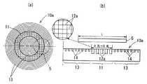
(参考例1)
図1は、本発明の参考例の研磨パッド10を示す図であり、同図(a)は平面図であり、同図(b)は、その半径方向に沿う拡大した断面図である。
【0026】
この参考例の研磨パッド10は、上述の図9に示されるCMP(化学機械研磨)装置の定盤1の表面に取付けられて被研磨物、例えば、半導体ウェハ5の化学機械研磨に用いられるものである。
【0027】
この研磨パッド10は、円板状であって、その表面に同心円状の複数の溝が加工されており、例えば、ポリウレタン等の樹脂からなる。
【0028】
この参考例では、半導体ウェハ5の研磨面の中心部分と周辺部分との研磨量の均一化を図って平坦性を向上させるために、次のように構成している。
【0029】
すなわち、この研磨パッド10は、半導体ウェハ5の研磨の際に、半導体ウェハ5の少なくとも中心部分が圧接される第1の領域11における第1の溝12の加工形態と、前記第1の領域11以外の第2の領域13における第2の溝14の加工形態とを異ならせている。
【0030】
半導体ウェハ5の中心部分が、圧接される第1の領域11は、同図(a)に示されるように、円板状の研磨パッド10の半径方向の中央部付近の環状の領域となっており、第2の領域13は、第1の領域11に囲まれた研磨パッド10の中心部を含む円形の領域および第1の領域11の外周の環状の領域となっている。
【0031】
ここで、同図(b)に示されるように、被研磨物である半導体ウェハ5の直径をLとすると、第1の領域11の幅は、例えば、被研磨物の中心部の0.2L〜0.4Lの範囲であるのが好ましい。
【0032】
従来では、上述のように、半導体ウェハの中心部分にスラリーが侵入するのが阻害されて、中心部分の研磨量が、周辺部分に比べて少なくなって研磨面が不均一になるという課題があった。
【0033】
そこで、この参考例では、研磨の際に、半導体ウェハ5の中心部分が圧接される第1の領域11では、第2の領域13に比べて溝内のスラリーの流量を増加させて半導体ウェハ5を均一に研磨できるように次のように構成している。
【0034】
すなわち、第1の領域11に形成されている同心円状の複数の第1の溝12は、半径方向に沿う断面形状が矩形であって、第2の領域13に形成されている同心円状の複数の第2の溝14に比べて、同図(b)に示されるように、溝深さを深くするとともに、幅を広くしており、溝12内を流動するスラリーの流量を増加させるように構成している。
【0035】
この参考例では、第1の溝12は、その深さが、例えば、0.2mm〜3mm、好ましくは、0.4mm〜2mmであり、溝幅は、0.2mm〜3mm、好ましくは、0.2mm〜1.5mmである。
【0036】
一方、第2の溝14は、第1の溝12よりも深さおよび幅が小さく、その深さが、例えば、0.1mm〜1.5mm、好ましくは、0.2mm〜1.0mmである。また、溝幅は、0.1mm〜1.5mm、好ましくは、0.2mm〜1.5mmである。
【0037】
以上の構成を有する研磨パッド10を、上述の図9に示されるCMP(化学機械研磨)装置の定盤1の表面に取付けて被研磨物、例えば、半導体ウェハ5の研磨を行なうものである。
【0038】
この研磨の際に、半導体ウェハ5の中心部分が圧接される第1の領域11の第1の溝12内を流動するスラリーの流量を、第2の領域の第2の溝14内を流動するスラリーの流量に比べて増加させることができる。したがって、半導体ウェハ5の中心部分では、周辺部分に比べて、化学的な研磨作用を強くすることができ、半導体ウェハ5の中心部分と周辺部分とで研磨量の均一化を図って研磨面の平坦性を向上させることができる。
【0039】
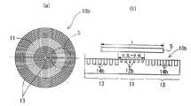
(参考例2)
図2は、本発明の他の参考例の研磨パッド10aを示す図であり、同図(a)は平面図であり、同図(b)は、その半径方向に沿う拡大した断面図であり、また、第1の領域11の一部を拡大した平面図を併せて示している。
【0040】
上述の参考例では、第1の領域11には、同心円状の複数の第1の溝12が形成されたのに対して、この参考例では、第1の領域11には、同心円状に代えて格子状の複数の第1の溝12aを形成している。
【0041】
この第1の領域11における格子状の第1の溝12aは、同図(b)に示されるように、第2の領域13の第2の溝14に比べて、溝の深さを深くするとともに、幅を広くし、溝12a内を流動するスラリーの流量を増加させるように構成している。
【0042】
その他の構成は、上述の参考例1と同様である。
【0043】
この参考例においても、半導体ウェハ5の中心部分が圧接される第1の領域11の第1の溝12a内のスラリーの流量を、第2の領域13の第2の溝14内のスラリーの流量に比べて増加させることによって、半導体ウェハ5の中心部分では、周辺部分に比べて、化学的な研磨作用を強くすることができ、これによって、半導体ウェハ5の中心部分と周辺部分とで研磨量の均一化を図って研磨面の平坦性を向上させることができる。
【0044】
(実施の形態1)
図3は、本発明の実施の形態に係る研磨パッド10bを示す図であり、同図(a)は平面図であり、同図(b)は、その半径方向に沿う拡大した断面図である。
【0045】
上述の各参考例では、半導体ウェハ5の中心部分が圧接される第1の領域11の溝12,12aを流動するスラリーの流量を、第2の領域13に比べて増加させることによって、半導体ウェハ5の中心部分では、周辺部分に比べて、化学的な研磨作用を強くするものであったのに対して、この実施の形態では、半導体ウェハ5の中心部分が圧接される第1の領域11では、第2の領域13に比べて、半導体ウェハ5との接触面積を増加させて機械的な研磨作用を強くするものである。
【0046】
ここで、接触面積とは、半導体ウェハ5が圧接される研磨パッドの領域における一定面積(単位面積)当たりについて、半導体ウェハ5と接触する面積をいう。
【0047】
この実施の形態では、第1の領域11の同心円状の複数の第1の溝12bは、第2の領域13の同心円状の複数の第2の溝14bに比べて、溝の幅を狭くするとともに、深さを浅くし、半導体ウェハ5との接触面積を増加させるように構成している。
【0048】
この実施の形態では、第1の溝12bは、その深さが、例えば、0.2mm〜3mm、好ましくは、0.4mm〜2mmであり、溝幅は、0.2mm〜3mm、好ましくは、0.2mm〜1.5mmである。
【0049】
一方、第2の溝14bは、第1の溝12bよりも深さおよび幅が大きく、その深さが、例えば、0.1mm〜1.5mm、好ましくは、0.2mm〜1.0mmである。また、溝幅は、0.1mm〜1.5mm、好ましくは、0.2mm〜1.5mmである。
【0050】
その他の構成は、上述の参考例1と同様である。
【0051】
この実施の形態では、半導体ウェハ5の中心部分が圧接される第1の領域11の接触面積を、第2の領域の接触面積に比べて増加させることによって、半導体ウェハ5の中心部分では、周辺部分に比べて、機械的な研磨作用を強くすることができ、これによって、半導体ウェハ5の中心部分と周辺部分とで研磨量の均一化を図って研磨面の平坦性を向上させることができる。
【0052】
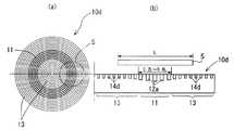
(実施の形態2)
図4は、本発明の他の実施の形態に係る研磨パッド10cを示す図であり、同図(a)は平面図であり、同図(b)は、その半径方向に沿う拡大した断面図であり、また、第2の領域13の一部を拡大した平面図を併せて示している。
【0053】
この実施の形態では、第1の領域11には、同心円状の複数の第1の溝12bを形成し、第2の領域13には、格子状の第2の溝14cを形成している。
【0054】
第1の溝12bは、同図(b)に示されるように、第2の溝14cに比べて、溝の幅が狭く形成されているとともに、浅く形成されており、これによって、第1の領域11では、半導体ウェハ5との接触面積を、第2の領域13に比べて増加させている。
【0055】
この実施の形態では、半導体ウェハ5の中心部分が圧接される第1の領域11の接触面積を、第2の領域13の接触面積に比べて増加させることによって、半導体ウェハ5の中心部分では、周辺部分に比べて、機械的な研磨作用を強くすることができ、これによって、半導体ウェハ5の中心部分と周辺部分とで研磨量の均一化を図って研磨面の平坦性を向上させることができる。
【0056】
【実施例】
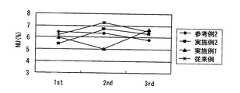
以下、上述の参考例2および実施の形態1,2にそれぞれ対応する参考例2,実施例1,2と従来例とについて、ヘッドの回転数を41rpm、プラテンの回転数を60rpm、面圧を7psiという研磨条件で、12インチの半導体ウェハの研磨を3回それぞれ行なって研磨レート(RR:Removal Rate)と、研磨面の面内不均一性(NU:Non Uniformity)とを計測した。なお、面内不均一性は、エリプソメータを用いて49点を計測し、NUを次式で算出した。
NU=(標準偏差/平均値)×100
その結果を、図5および図6に示す。
【0057】
従来例は、第1,第2の領域の区別なく、研磨パッドの略全面に同心円状の溝が形成されているものを用いた。
【0058】
ここで、参考例2、実施例1,2および従来例の各領域および溝サイズについて、説明する。
【0059】
研磨パッドの直径は、200mmであり、第1の領域は、12インチのウェハの中心部の60mmの領域、すなわち、被研磨物の直径Lの内の0.3Lの領域であった、
参考例2の第1の溝12aの深さは、1mm、幅は、1mmであり、第2の溝14の深さは、0.5mm、幅は、0.5mmである。
【0060】
実施例1の第1の溝12bの深さは、0.5mm、幅は、0.5mmであり、第2の溝14bの深さは、1mm、幅は、1mmである。
【0061】
実施例2の第1の溝12bの深さは、0.5mm、幅は、0.5mmであり、第2の溝14cの深さは、1mm、幅は、1mmである。
【0062】
従来例の溝深さは、0.5mm、幅は0.5mmである。
【0063】
図5に示されるように、研磨レートは、いずれの実施例も従来例と同等あるいはそれよりも良好であった。
【0064】
また、図6に示されるように、面内不均一性も従来例に比べて低く、平坦性が向上した。
【0065】
(その他の実施の形態)
上述の各実施の形態では、第1の領域11と第2の領域13との境界を境にして溝の加工形態を急激に異ならせけれども、本発明の他の実施の形態として、例えば、図7(b)に示されるように、溝の深さなどを徐々に異ならせるようにしてもよい。
【0066】
上述の実施の形態1,2では、第2の領域13の第2の溝14b,14cは、第1の領域11の第1の溝12bに比べて、溝の深さが大きく、スラリーの流量が増加することになるが、本発明の他の実施の形態として、例えば、図8(b)に示されるように、第2の領域13の第2の溝14eを、浅くしてスラリーの流量が、第1の領域11に比べて増加しないようにしてもよい。
【0067】
上述の各実施の形態では、溝の断面形状は、矩形であったけれども、V字状、U字状、台形状、その他の形状であってもよい。
【0068】
なお、研磨パッドの表面には、第1の領域11、第2の領域13以外の領域を設けてもよい。
【0069】
【発明の効果】
以上のように本発明よれば、被研磨物の中心部分と周辺部分とでスラリーの流量や当該研磨パッドとの接触面積を異ならせることが可能となり、被研磨物の中心部分と周辺部分とで、機械的な研磨作用を調節して研磨量の均一化を図り、研磨面の平坦性を向上させることができる。
【図面の簡単な説明】
【図1】本発明の参考例の研磨パッドを示す図
【図2】本発明の他の参考例の研磨パッドを示す図
【図3】本発明の実施の形態の研磨パッドを示す図
【図4】本発明の他の実施の形態の研磨パッドを示す図
【図5】本発明の実施例、参考例および従来例の研磨レートを示す図
【図6】本発明の実施例、参考例および従来例の面内不均一性を示す図
【図7】本発明の他の実施の形態の研磨パッドを示す図
【図8】本発明の更に他の実施の形態の研磨パッドを示す図
【図9】CMP装置の概略構成図
【符号の説明】
3 スラリー 5 半導体ウェハ
10,10a〜10e 研磨パッド 11 第1の領域
13 第2の領域 12,12a,12b,12d 第1の溝
14,14b〜14e 第2の溝[0001]
BACKGROUND OF THE INVENTION
The present invention relates to a polishing pad suitable for chemical mechanical polishing (CMP) used, for example, when performing planarization processing of an object to be polished such as a semiconductor wafer in a manufacturing process of a semiconductor manufacturing apparatus.
[0002]
[Prior art]
Conventionally, various CMP apparatuses have been proposed (see, for example, Patent Document 1).
[0003]
FIG. 9 is a schematic configuration diagram of a conventional CMP apparatus. A
[0004]
The
[0005]
[Patent Document 1]
Japanese Patent Laid-Open No. 2000-334655 [0006]
[Problems to be solved by the invention]
In such a CMP apparatus, as described above, an object to be polished such as a semiconductor wafer is pressed against and in pressure contact with the polishing pad. Therefore, the flow of slurry between the object to be polished and the polishing pad is hindered. In particular, the entry of the slurry into the central portion of the object to be polished is hindered. As a result, the polishing amount of the central portion of the object to be polished is smaller than that of the peripheral portion, and the tendency becomes remarkable particularly in a semiconductor wafer having a large area.
[0007]
The present invention has been made in view of the above points, and an object thereof is to improve the flatness by uniformly polishing an object to be polished.
[0008]
[Means for Solving the Problems]
The present invention is configured as follows in order to achieve the above-described object.
[0009]
That is, the polishing pad of the present invention is a polishing pad that is used for polishing an object to be polished and has a plurality of recesses formed on the surface thereof, and a first region in which a central portion of the object to be polished is press-contacted. And a second region other than the first region,wherein the first region is an annular region near the center of the disk-shaped polishing pad in the radial direction, and the second region is The contact area with the object to be polished per unit area in the firstarea, which is the area on both sides of the first area, and the object to be polished is pressed, A processing mode of the recess in the first region and a processing mode of the recess in the second region so as to be larger than a contact area with the object to be polished per unit area in the second region.Rutotomoni with differentbets, and the recess grooves There.
[0011]
In addition, the processing pattern of the recess means the shape of the recess that appears as a shape by processing, for example, a processing pattern of the recess such as concentric circles, a lattice shape, or a spiral, or the pitch of the recess, the planar shape or the cross-sectional shape of the recess Etc.
[0012]
In addition, the first region where the central portion of the object to be polished is pressed is a region where the central portion of the object to be polished such as a semiconductor wafer is pressed against the rotating polishing pad, and at least the central portion is What is necessary is just to press-contact, and parts other than a center part may be press-contacted.
[0013]
The second region refers to a region other than the first region, and preferably refers to a region in which a portion other than the central portion of an object to be polished such as a semiconductor wafer is pressed against the rotating polishing pad.
[0014]
According to the present invention,by varying the processing form of depression in the first region where the central portion of the workpiece is pressed against, and processed forms of recesses in the second region where the peripheral portion of the workpiece is pressed againstSince the contact area with the object to be polished in the first region is larger than the contact area with the object to be polished in the second region , the central partof the object to be polished iscompared with the peripheral part. The mechanical polishing action can bestrengthened, whereby the amount of polishing can be made uniformbetween the central portion and the peripheral portion of the object to be polished, and the flatness of the polished surface can be improved.
[0017]
In a preferred embodiment, the cross-sectional shape along the radial direction of the groove in the first region is different from the cross-sectional shape along the radial direction of the groove in the second region.
[0018]
According to this embodiment, by varying the groove cross-sectional shape, it may bein the central portion and the peripheral portion of the object to bepolished, different contact area betweenthose the polishing pad.Therefore, in the central part of theobject to be polished,as compared with the peripheralportion, by strong mechanical polishing action to increase the contact area betweenthose the polishing pad, with the central portion and the peripheral portion of the workpiece The flatness of the polished surface can be improved by making the polishing amount uniform.
[0019]
In another embodiment, the plurality of grooves is formed in concentric circles, the cross-sectional shape is rectangular,the width of the groove in said firstregion,said groove in said second regionIt is narrower than the width.
[0020]
According to this embodiment, by varying thewidth of the groove concentric rectangular cross-section,with a central portion and a peripheral portion of the object to bepolished, with different contact area betweenthose the polishing pad, thereby, be polished The flatness of the polished surface can be improved by making the polishing amount uniform between the central portion and the peripheral portion of the object.
[0021]
In still another embodiment, the groove in one of the first and second regions is a concentric groove, and the groove in the other region is a lattice-like groove.
[0022]
According to this embodiment, by varying the processing pattern of groovesin the central portion and the peripheral portion of the object to bepolished, with different contact area betweenthose the polishing pad, whereby the central portion of the workpiece The flatness of the polished surface can be improved by making the polishing amount uniform between the peripheral portion and the peripheral portion.
[0023]
DETAILED DESCRIPTION OF THE INVENTION
Hereinafter, embodiments of the present invention will be described in detail with reference to the drawings.
[0024]
Here, a reference example will be described prior to the description of the embodiment of the present invention.
[0025]
(Reference Example 1)
FIG. 1 is a view showinga
[0026]
The
[0027]
The
[0028]
In thisreference example , in order to improve the flatness by making the polishing amount uniform between the central portion and the peripheral portion of the polishing surface of the
[0029]
That is, the
[0030]
The
[0031]
Here, as shown in FIG. 4B, when the diameter of the
[0032]
Conventionally, as described above, the entry of slurry into the central portion of the semiconductor wafer is hindered, and the amount of polishing in the central portion becomes smaller than that in the peripheral portion, resulting in a non-uniform polishing surface. It was.
[0033]
Therefore, in thisreference example , the flow rate of the slurry in the groove is increased in the
[0034]
That is, the plurality of concentric
[0035]
In thisreference example , the
[0036]
On the other hand, the
[0037]
The
[0038]
At the time of this polishing, the flow rate of the slurry flowing in the
[0039]
(Reference Example 2)
FIG. 2 is a view showinga
[0040]
In the above-describedreference example , a plurality of concentric
[0041]
The lattice-shaped
[0042]
Other configurations are the same as those inReference Example 1 described above.
[0043]
Also in thisreference example , the flow rate of the slurry in the
[0044]
(Embodiment1 )
Figure 3 is a view showing a
[0045]
In each of thereference examples described above, by increasing the flow rate of the slurry flowing through the
[0046]
Here, the contact area refers to an area in contact with the
[0047]
In this embodiment, the plurality of concentric
[0048]
In this embodiment, the
[0049]
On the other hand, the
[0050]
Other configurations are the same as those inReference Example 1 described above.
[0051]
In this embodiment, by increasing the contact area of the
[0052]
(Embodiment2 )
FIG. 4 is a view showing a
[0053]
In this embodiment, a plurality of concentric
[0054]
As shown in FIG. 2B, the
[0055]
In this embodiment, by increasing the contact area of the
[0056]
【Example】
Hereinafter,Reference Example 2 respectively inReference Example 2 and thefirst and second embodiments described abovecorresponds, for the conventional example as in Example1, 41Rpm the rotational speed of the head, the rotational speed of the platen 60 rpm, the surface pressure Under a polishing condition of 7 psi, a 12-inch semiconductor wafer was polished three times, and the polishing rate (RR: Removal Rate) and in-plane non-uniformity (NU: Non Uniformity) were measured. The in-plane non-uniformity was obtained by measuring 49 points using an ellipsometer and calculating NU by the following equation.
NU = (standard deviation / average value) × 100
The results are shown in FIG. 5 and FIG.
[0057]
In the conventional example, a concentric groove formed on substantially the entire surface of the polishing pad is used without distinguishing between the first and second regions.
[0058]
Here, each region and groove size inReference Example 2, Examples1 and2 and the conventional example will be described.
[0059]
The diameter of the polishing pad was 200 mm, and the first area was a 60 mm area in the center of a 12-inch wafer, that is, a 0.3 L area within the diameter L of the object to be polished.
The
[0060]
The
[0061]
The
[0062]
The groove depth of the conventional example is 0.5 mm, and the width is 0.5 mm.
[0063]
As shown in FIG. 5, the polishing rate in each example was equal to or better than that in the conventional example.
[0064]
Further, as shown in FIG. 6, the in-plane non-uniformity is lower than that of the conventional example, and the flatness is improved.
[0065]
(Other embodiments)
In each of the above-described embodiments, although the processing form of the groove is abruptly changed at the boundary between the
[0066]
In thefirst and second embodiments described above, the
[0067]
In each of the above-described embodiments, the cross-sectional shape of the groove is rectangular, but it may be V-shaped, U-shaped, trapezoidal, or other shapes.
[0068]
An area other than the
[0069]
【The invention's effect】
According the present invention as described above, betweenthe center portion and the at it is possible to vary the contact area between the slurry flow rate and the polishing pad peripheral portion, the central portion and the peripheral portion of the object to be polished of the object to be polished, achieving uniformity of polishing amount by adjusting themachine械的polishing action, it is possible to improve the flatness of the polished surface.
[Brief description of the drawings]
It shows a polishing pad in the form ofimplementation of the other figures showing a polishing pad ofExample 3 shows the present invention in FIG. 2 shows the present invention showing a polishing pad of thereference example of the invention, FIG [ 4] example of the figure showing a polishing pad of another embodiment of the invention the present invention;FIG, reference examples and the embodiment of FIG. 6 present invention showing the polishing rate of the priorart, reference example FIG. 7 is a diagram showing in-plane non-uniformity of a conventional example. FIG. 7 is a diagram showing a polishing pad according to another embodiment of the present invention. FIG. 8 is a diagram showing a polishing pad according to still another embodiment of the present invention. FIG. 9 is a schematic configuration diagram of a CMP apparatus.
3
Claims (4)
Translated fromJapanese前記被研磨物の中心部分が圧接される第1の領域と、前記第1の領域以外の第2の領域とを備え、前記第1の領域が、円板状の当該研磨パッドの半径方向の略中央付近の環状の領域であり、前記第2の領域が、前記第1の領域の両側の領域であり、
前記被研磨物が圧接される前記第1の領域における単位面積当たりの前記被研磨物との接触面積が、前記被研磨物が圧接される前記第2の領域における前記単位面積当たりの前記被研磨物との接触面積に比べて大きくなるように、前記第1の領域における前記窪みの加工形態と、前記第2の領域における前記窪みの加工形態とを異ならせると共に、前記窪みを溝としたことを特徴とする研磨パッド。A polishing pad used for polishing an object to be polished and having a plurality of depressions processed on the surface,
A first region in which a central portion of the object to be polished is pressed, and a second region other than the first region,wherein the first region is in a radial direction of the disk-shaped polishing pad. An annular region near the center, and the second region is a region on both sides of the first region,
The contact area with the object to be polished per unit area in the first region to which the object to be polished is pressed is equal to the object to be polished per unit area in the second area to which the object to be polished is pressed. to be larger than the contact area between the object and the processed forms of said recess in said first region, said secondRutotomoni made different from the processed forms of the recess in theregion, and with the recess grooves A polishing pad characterized by that.
前記第1の領域における前記溝の前記半径方向に沿う断面形状を、前記第2の領域における前記溝の前記半径方向に沿う断面形状と異ならせた研磨パッド。The polishing pad according to claim1 , wherein
A polishing pad, wherein a cross-sectional shape of the groove in the first region along the radial direction is different from a cross-sectional shape of the groove in the second region along the radial direction.
前記複数の溝は、同心円状に形成されるとともに、前記断面形状が矩形であり、前記第1の領域における前記溝の幅を、前記第2の領域における前記溝の幅よりも狭くした研磨パッド。The polishing pad according to claim2 , wherein
The plurality of grooves are formed concentrically, the cross-sectional shape is rectangular, and the width of the grooves in the first region is smaller than the width of the grooves in the second region .
前記第1,第2の領域の内の一方の領域における前記溝を、同心円状の溝とし、他方の領域における溝を、格子状の溝とした研磨パッド。The polishing pad according to claim1 or2 ,
A polishing pad, wherein the groove in one of the first and second regions is a concentric groove, and the groove in the other region is a lattice-like groove.
Priority Applications (1)
| Application Number | Priority Date | Filing Date | Title |
|---|---|---|---|
| JP2003117776AJP4478859B2 (en) | 2003-04-23 | 2003-04-23 | Polishing pad |
Applications Claiming Priority (1)
| Application Number | Priority Date | Filing Date | Title |
|---|---|---|---|
| JP2003117776AJP4478859B2 (en) | 2003-04-23 | 2003-04-23 | Polishing pad |
Publications (2)
| Publication Number | Publication Date |
|---|---|
| JP2004327567A JP2004327567A (en) | 2004-11-18 |
| JP4478859B2true JP4478859B2 (en) | 2010-06-09 |
Family
ID=33497525
Family Applications (1)
| Application Number | Title | Priority Date | Filing Date |
|---|---|---|---|
| JP2003117776AExpired - LifetimeJP4478859B2 (en) | 2003-04-23 | 2003-04-23 | Polishing pad |
Country Status (1)
| Country | Link |
|---|---|
| JP (1) | JP4478859B2 (en) |
Families Citing this family (14)
| Publication number | Priority date | Publication date | Assignee | Title |
|---|---|---|---|---|
| KR100818523B1 (en)* | 2006-08-17 | 2008-03-31 | 동부일렉트로닉스 주식회사 | Polishing pad |
| JP2008258574A (en)* | 2007-03-14 | 2008-10-23 | Jsr Corp | Chemical mechanical polishing pad and chemical mechanical polishing method |
| JP5284610B2 (en)* | 2007-08-20 | 2013-09-11 | 八千代マイクロサイエンス株式会社 | Rotating surface plate for double-sided lapping machine |
| JP5585081B2 (en)* | 2008-05-16 | 2014-09-10 | 東レ株式会社 | Polishing pad |
| JP5222320B2 (en)* | 2010-05-25 | 2013-06-26 | 東洋ゴム工業株式会社 | Polishing pad and semiconductor device manufacturing method |
| KR101232787B1 (en) | 2010-08-18 | 2013-02-13 | 주식회사 엘지화학 | Polishing-Pad for polishing system |
| JP5635957B2 (en) | 2010-09-09 | 2014-12-03 | 日本碍子株式会社 | Polishing method of polishing object and polishing pad |
| TWI532565B (en)* | 2011-03-21 | 2016-05-11 | 智勝科技股份有限公司 | Polishing method and polishing system |
| US10864612B2 (en)* | 2016-12-14 | 2020-12-15 | Taiwan Semiconductor Manufacturing Company, Ltd. | Polishing pad and method of using |
| CN114473855A (en)* | 2020-10-28 | 2022-05-13 | 中国科学院微电子研究所 | A kind of grinding pad and chemical mechanical polishing equipment |
| JP7570903B2 (en) | 2020-12-01 | 2024-10-22 | 富士紡ホールディングス株式会社 | Polishing Pad |
| CN113878491A (en)* | 2021-10-20 | 2022-01-04 | 北京烁科精微电子装备有限公司 | Grinding pad and grinding device with densely distributed branches and leaves and grooves |
| CN114310627A (en)* | 2021-12-30 | 2022-04-12 | 西安奕斯伟材料科技有限公司 | Polishing pad and polishing equipment for polishing silicon wafer |
| CN115070606B (en)* | 2022-06-30 | 2023-11-14 | 西安奕斯伟材料科技股份有限公司 | Polishing pad and polishing equipment for polishing silicon wafer |
- 2003
- 2003-04-23JPJP2003117776Apatent/JP4478859B2/ennot_activeExpired - Lifetime
Also Published As
| Publication number | Publication date |
|---|---|
| JP2004327567A (en) | 2004-11-18 |
Similar Documents
| Publication | Publication Date | Title |
|---|---|---|
| JP4478859B2 (en) | Polishing pad | |
| JP5208467B2 (en) | CMP pad with unevenly spaced grooves | |
| TW567109B (en) | Method and apparatus for polishing outer peripheral chamfered part of wafer | |
| JP3075510B2 (en) | Substrate polishing method and apparatus | |
| KR100818523B1 (en) | Polishing pad | |
| US6458023B1 (en) | Multi characterized chemical mechanical polishing pad and method for fabricating the same | |
| CN112959212B (en) | Chemical mechanical polishing pad with optimized grooves and application thereof | |
| US6544107B2 (en) | Composite polishing pads for chemical-mechanical polishing | |
| KR20010089245A (en) | Manufacturing process for semiconductor wafer | |
| US6620035B2 (en) | Grooved rollers for a linear chemical mechanical planarization system | |
| US8662961B2 (en) | Polishing pad seasoning method, seasoning plate, and semiconductor polishing device | |
| JP3502550B2 (en) | Polishing equipment | |
| KR100506814B1 (en) | Apparatus for polishing a wafer | |
| CN114378715B (en) | Chemical mechanical polishing pad and polishing method | |
| US6592429B1 (en) | Method and apparatus for controlling wafer uniformity in a chemical mechanical polishing tool using carrier head signatures | |
| KR100886603B1 (en) | Apparatus for polishing wafer and process for polishing wafer | |
| JP3937294B2 (en) | Polishing equipment | |
| JP3019849B1 (en) | Chemical mechanical polishing equipment | |
| JP4449905B2 (en) | Polishing cloth, polishing cloth processing method, and substrate manufacturing method using the same | |
| KR102685134B1 (en) | Polishing pad having improved polishing speed and chemical mechanical polishing apparatus including the same | |
| JP2004047801A (en) | Polishing process of semiconductor wafer | |
| TWI276509B (en) | Sandpaper for polishing carrier film | |
| JP3992307B2 (en) | Plate for polishing thin plate and method for manufacturing the same | |
| JP2002208575A (en) | Semiconductor grinding device | |
| JP2002124492A (en) | Semiconductor manufacturing equipment |
Legal Events
| Date | Code | Title | Description |
|---|---|---|---|
| A621 | Written request for application examination | Free format text:JAPANESE INTERMEDIATE CODE: A621 Effective date:20060404 | |
| A977 | Report on retrieval | Free format text:JAPANESE INTERMEDIATE CODE: A971007 Effective date:20080922 | |
| A131 | Notification of reasons for refusal | Free format text:JAPANESE INTERMEDIATE CODE: A131 Effective date:20080930 | |
| A521 | Request for written amendment filed | Free format text:JAPANESE INTERMEDIATE CODE: A523 Effective date:20081126 | |
| A02 | Decision of refusal | Free format text:JAPANESE INTERMEDIATE CODE: A02 Effective date:20090818 | |
| A521 | Request for written amendment filed | Free format text:JAPANESE INTERMEDIATE CODE: A523 Effective date:20091112 | |
| A521 | Request for written amendment filed | Free format text:JAPANESE INTERMEDIATE CODE: A523 Effective date:20091202 | |
| A911 | Transfer to examiner for re-examination before appeal (zenchi) | Free format text:JAPANESE INTERMEDIATE CODE: A911 Effective date:20091207 | |
| TRDD | Decision of grant or rejection written | ||
| A01 | Written decision to grant a patent or to grant a registration (utility model) | Free format text:JAPANESE INTERMEDIATE CODE: A01 Effective date:20100216 | |
| A01 | Written decision to grant a patent or to grant a registration (utility model) | Free format text:JAPANESE INTERMEDIATE CODE: A01 | |
| A61 | First payment of annual fees (during grant procedure) | Free format text:JAPANESE INTERMEDIATE CODE: A61 Effective date:20100303 | |
| FPAY | Renewal fee payment (event date is renewal date of database) | Free format text:PAYMENT UNTIL: 20130326 Year of fee payment:3 | |
| R150 | Certificate of patent or registration of utility model | Ref document number:4478859 Country of ref document:JP Free format text:JAPANESE INTERMEDIATE CODE: R150 Free format text:JAPANESE INTERMEDIATE CODE: R150 | |
| FPAY | Renewal fee payment (event date is renewal date of database) | Free format text:PAYMENT UNTIL: 20140326 Year of fee payment:4 | |
| S533 | Written request for registration of change of name | Free format text:JAPANESE INTERMEDIATE CODE: R313533 | |
| R350 | Written notification of registration of transfer | Free format text:JAPANESE INTERMEDIATE CODE: R350 | |
| EXPY | Cancellation because of completion of term |