JP4474532B2 - Signal generation system - Google Patents
Signal generation systemDownload PDFInfo
- Publication number
- JP4474532B2 JP4474532B2JP2007337324AJP2007337324AJP4474532B2JP 4474532 B2JP4474532 B2JP 4474532B2JP 2007337324 AJP2007337324 AJP 2007337324AJP 2007337324 AJP2007337324 AJP 2007337324AJP 4474532 B2JP4474532 B2JP 4474532B2
- Authority
- JP
- Japan
- Prior art keywords
- signal generator
- signal
- clock
- sampling clock
- phase
- Prior art date
- Legal status (The legal status is an assumption and is not a legal conclusion. Google has not performed a legal analysis and makes no representation as to the accuracy of the status listed.)
- Expired - Fee Related
Links
Images


Classifications
- G—PHYSICS
- G06—COMPUTING OR CALCULATING; COUNTING
- G06F—ELECTRIC DIGITAL DATA PROCESSING
- G06F1/00—Details not covered by groups G06F3/00 - G06F13/00 and G06F21/00
- G06F1/02—Digital function generators
- G06F1/03—Digital function generators working, at least partly, by table look-up
- G06F1/0321—Waveform generators, i.e. devices for generating periodical functions of time, e.g. direct digital synthesizers
- G—PHYSICS
- G01—MEASURING; TESTING
- G01R—MEASURING ELECTRIC VARIABLES; MEASURING MAGNETIC VARIABLES
- G01R31/00—Arrangements for testing electric properties; Arrangements for locating electric faults; Arrangements for electrical testing characterised by what is being tested not provided for elsewhere
- G01R31/28—Testing of electronic circuits, e.g. by signal tracer
- G01R31/317—Testing of digital circuits
- G01R31/3181—Functional testing
- G01R31/319—Tester hardware, i.e. output processing circuits
- G01R31/31917—Stimuli generation or application of test patterns to the device under test [DUT]
- G01R31/31922—Timing generation or clock distribution
Landscapes
- Engineering & Computer Science (AREA)
- Physics & Mathematics (AREA)
- General Engineering & Computer Science (AREA)
- General Physics & Mathematics (AREA)
- Theoretical Computer Science (AREA)
- Tests Of Electronic Circuits (AREA)
- Stabilization Of Oscillater, Synchronisation, Frequency Synthesizers (AREA)
Description
Translated fromJapanese複数の信号発生装置をケーブルで接続して構成される信号発生システムに関し、特にサンプリング・クロックの周波数を変更したときに、複数の信号発生装置からの出力信号間の位相を自動的に合わせることができる信号発生システムに関する。 For signal generation systems configured by connecting multiple signal generators with cables, especially when the sampling clock frequency is changed, the phases between the output signals from the multiple signal generators can be automatically adjusted. It is related with the signal generation system which can be performed.
信号発生装置は、ユーザが任意の波形データを設定することで、その波形データに対応する電気信号を出力できる装置である。こうした信号発生装置としては、例えば、米国テクロニクス社製AWG7000シリーズ任意波形ゼネレータが知られている。これは、例えば、被測定回路の動作に必要な信号を信号発生装置から供給し、被測定回路から出力される信号をオシロスコープなどで測定することで、被測定回路が正常に動作しているか否か確認するために使用される。 The signal generator is an apparatus that can output an electrical signal corresponding to the waveform data when the user sets arbitrary waveform data. As such a signal generator, for example, an AWG7000 series arbitrary waveform generator manufactured by Tecronics, Inc. is known. For example, whether or not the circuit under test is operating normally by supplying a signal necessary for the operation of the circuit under test from a signal generator and measuring the signal output from the circuit under test with an oscilloscope or the like. Used to check if.
信号発生装置は、1台で2又は4チャンネルの信号を一度に出力できるものが多い。もしこれ以上のチャンネル数の信号を出力したければ、複数の信号発生装置を用いる方法が考えられるが、この場合、異なる信号発生装置から出力される出力信号間の位相をどのように合わせるかが課題となる。 Many signal generators can output 2 or 4 channel signals at one time. If you want to output a signal with more channels than this, you can use a method that uses multiple signal generators. In this case, how to adjust the phase between the output signals output from different signal generators It becomes a problem.
従来、複数の信号発生装置の内の1つをマスタとして、その基準発振信号を外部の分配増幅器に供給し、分配増幅器がマスタの基準発振信号を増幅して他の信号発生装置(スレーブ)に供給することで、複数の信号発生器から位相差が固定され、共通の単一周波数の信号を出力する方法が知られている。これについては、例えば、非特許文献1として示す米国アジレント・テクノロジー社の「PSG Signal Generators Brochure」第20頁に、Z5623AK05型分配増幅器(Distribution Amplifier)を用いて、最大8台の米国アジレント・テクノロジー社製E8267D型PSGベクトル信号発生器から位相同期信号を発生させることが開示されている。 Conventionally, one of a plurality of signal generators is used as a master, the reference oscillation signal is supplied to an external distribution amplifier, and the distribution amplifier amplifies the master reference oscillation signal to another signal generation device (slave). A method is known in which a phase difference is fixed from a plurality of signal generators and a common single frequency signal is output by supplying the signals. For example, a
ところで、信号発生装置には、装置の外部に設けた回路等から出力される特定の信号や、ユーザの操作パネルの操作に応じて信号の出力を開始するトリガ機能がある。また、装置の外部に設けた回路から出力される特定の信号や、ユーザの操作パネルの操作に応じて出力信号の種類を変更するイベント機能がある。こうしたトリガ/イベントに応じた信号の出力開始/出力信号の変更時においても、複数の信号発生装置の出力信号間の位相関係を適切に維持できる必要がある。 By the way, the signal generation device has a trigger function for starting output of a specific signal output from a circuit or the like provided outside the device, or in response to a user operation on the operation panel. In addition, there is an event function for changing the type of an output signal in accordance with a specific signal output from a circuit provided outside the apparatus or a user operation on an operation panel. Even at the start of output of a signal according to such a trigger / event / change of the output signal, it is necessary to appropriately maintain the phase relationship between the output signals of the plurality of signal generators.
本発明による信号発生システムは、複数の信号発生装置からタイミング(トリガ/イベント)信号に応じてデータ(信号)を出力する場合にあっても、複数の信号発生装置の出力データ間の位相関係を自動的に調整するものである。各信号発生装置は、周波数可変なサンプリング・クロックを供給するサンプリング・クロック供給手段と、サンプリング・クロックを分周して分周クロックを供給する分周手段と、データの供給順序を制御するシーケンス制御手段と、データを分周クロックに従って供給する波形記憶手段と、データの供給タイミングを制御するタイミング信号をシーケンス制御手段に供給するタイミング制御手段と、データをサンプリング・クロック単位で遅延できる遅延手段と、遅延手段から受けたデータを並直列変換して高速データとしてサンプリング・クロックに従って出力する並直列変換手段と、各手段の制御を行う中央制御手段とを夫々有する。これらの信号発生装置間は、専用の同軸ケーブルなどで接続され、こうした同軸ケーブルとその周辺回路を含む通信手段により、第1信号発生装置のサンプリング・クロック及びタイミング信号を第2信号発生装置に供給すると共に、第1及び第2信号発生装置夫々の中央制御手段間で情報を通信する。このとき、第2信号発生装置は、第2信号発生装置のサンプリング・クロック供給手段が供給するサンプリング・クロックの代わりとして、第1信号発生装置が供給するサンプリング・クロックを使用する。また、第2信号発生装置のタイミング制御手段は、第1信号発生装置が供給するタイミング信号を受け、このタイミング信号を第2信号発生装置のシーケンス制御手段に供給する。通信手段における信号の遅延量は、専用の同軸ケーブル等を使用するので、既知とする。しかしながら、第1信号発生装置から供給されるサンプリング・クロック等に従って第2信号発生装置が動作するので、通信手段における信号の遅延量が固定であっても、もしサンプリング・クロックの周波数が変更されると、通信手段の遅延量に相当するサンプリング・クロックのクロック数は変化する。そこで、本発明では、第1信号発生装置のサンプリング・クロックの周波数が変更されたときに、第1又は第2信号発生装置の中央制御手段は、通信手段における遅延量を周波数の変更後のサンプリング・クロックのクロック数で表した値を計算し、クロック数に応じて第1信号発生装置の遅延手段がデータを遅延することにより、第1及び第2信号発生装置で生成する高速データの位相関係を調整することを特徴とする。The signal generation system according to the present invention has a phase relationship between output data of a plurality of signal generators even when data (signals) are output from a plurality of signal generators according to timing (trigger / event) signals. It adjusts automatically. Each signal generator includes a sampling clock supply means for supplying a sampling clock having a variable frequency, a frequency dividing means for dividing the sampling clock to supply a divided clock, and a sequence control for controlling the data supply sequence Means, waveform storage means for supplying data according to the divided clock, timing control means for supplying a timing signal for controlling the data supply timing to the sequence control means, delay means for delaying the data in units of sampling clocks, Parallel-serial conversion means for parallel-serial conversion of data received from the delay means and outputting as high-speed data according to a sampling clock, and central control means for controlling each means are provided. Betweenthese signals generating device is connected, such as by a dedicated coaxial cable, by this coaxial cable and communication means including a peripheral circuit, a sampling clock and timing signals of the first signal generating device to a second signal generator In addition, the information is communicated between the central control means of the first and second signal generators. At this time,the second signal generator uses the sampling clock supplied by the first signal generator instead of the sampling clock supplied by the sampling clock supply means of the second signal generator. The timing control means of the second signal generator receives the timing signal supplied from the first signal generator and supplies this timing signal to the sequence control means of the second signal generator. The amount of signal delay in the communication means is known because a dedicated coaxial cable or the like is used. However, since the second signal generator operates in accordance with the sampling clock supplied from the first signal generator, the frequency of the sampling clock is changed even if the signal delay amount in the communication means is fixed. Then, the number of sampling clocks corresponding to the delay amount of the communication means changes. Therefore, in the present invention, when the frequency of the sampling clock of the first signal generator is changed, the central control means of the first or second signal generator changes the delay amount in the communication means to the sampling after the frequency change. A phase relationship between high-speed data generated by the first and second signal generators by calculating a value represented by the number of clocks and delaying the data by the delay means of the first signal generator according to the number of clocks. It is characterized by adjusting.
また、更に精密に複数信号発生装置からの出力データの位相関係を調整するため、通信手段の遅延量に相当するサンプリング・クロックのクロック数に加えて、1クロックに満たないサンプリング・クロックの位相分も併せて計算し、位相調整するようにしても良い。このため、第1及び第2信号発生装置が、分周手段に供給するサンプリング・クロックの位相を調整する第1サンプリング・クロック位相調整手段と、並直列変換手段に供給するサンプリング・クロックの位相を調整する第2サンプリング・クロック位相調整手段とを更に有するようにすると良い。その上で、第1信号発生装置のサンプリング・クロックの周波数が変更されたときに、第1又は第2信号発生装置の中央制御手段は、通信手段における遅延量を周波数の変更後のサンプリング・クロックのクロック数及びクロック位相で表した値を計算し、クロック数で表した値に応じて第1信号発生装置の遅延手段がデータを遅延すると共に、クロック位相で表した値に応じて第1又は第2信号発生装置の第1及び第2サンプリング・クロック位相調整手段が供給するサンプリング・クロックの位相を調整することにより、第1及び第2信号発生装置で生成する高速データの位相関係を調整するにすると良い。In addition, in order to adjust the phase relationship of the output data from the multiple signal generators more precisely, in addition to the number of sampling clocks corresponding to the delay amount of the communication means, the phase of the sampling clock that is less than one clock. May also be calculated and the phase adjusted. Therefore, the first and second signal generators adjust the phase of the sampling clock supplied to the frequency dividing means, and the phase of the sampling clock supplied to the parallel-serial conversion means. It is preferable to further include second sampling clock phase adjusting means for adjusting. In addition, when the frequency of the sampling clock of the first signal generator is changed, the central control means of the first or second signal generator changes the delay amount in the communication means to the sampling clock after the frequency change. And the delay means of the first signal generator delays the data according to thevalue represented by the clock number, and the first or the second according to thevalue represented by the clock phase. The phase relationship of the high-speed data generated by the first and second signal generators is adjusted by adjusting the phase of the sampling clock supplied by the first and second sampling clock phase adjusting means of the second signal generator. It is good to make it.
また、位相関係の計算を容易にするため、第1及び第2信号発生装置を通信手段で接続した際に、通信手段が第1信号発生装置の分周クロックも第2信号発生装置に供給し、初期設定として、第1信号発生装置からの分周クロックと第2信号発生装置の分周クロックの位相を合わせるようにすると良い。その後のサンプリング・クロックの周波数変更によって両分周クロックの位相はずれていくが、このように最初に合わせておくことで、位相調整用のクロック数の計算を担当する第1又は第2信号発生装置の中央演算装置は、第1及び第2信号発生装置から出力される信号の位相関係を確実の把握できる。この位相比較のために、第2信号発生装置が分周クロック位相比較手段を更に有すると良い。そして、分周クロック位相比較手段を用いて第1及び第2信号発生装置の分周クロックの位相を一致させた後に、第1又は第2信号発生装置の中央制御手段が、通信手段における遅延量を周波数の変更後のサンプリング・クロックのクロック数で表した値を計算するようにする。 In order to facilitate the calculation of the phase relationship, when the first and second signal generators are connected by the communication means, the communication means also supplies the divided clock of the first signal generator to the second signal generator. As an initial setting, the phase of the frequency-divided clock from the first signal generator and the frequency-divided clock of the second signal generator may be matched. The phase of both frequency-divided clocks is shifted by the subsequent change in the frequency of the sampling clock, but the first or second signal generator in charge of calculating the number of clocks for phase adjustment can be obtained by matching them first in this way. The central processing unit can reliably grasp the phase relationship between the signals output from the first and second signal generators. For this phase comparison, it is preferable that the second signal generator further includes a divided clock phase comparison means. Then, after using the divided clock phase comparison means to match the phases of the divided clocks of the first and second signal generating devices, the central control means of the first or second signal generating device determines the delay amount in the communication means. Is calculated by the number of sampling clocks after the frequency change.
第2信号発生装置では、分周クロックで第1信号発生装置から供給されるタイミング(トリガ/イベント)信号を検出するので、サンプリング・クロックの周波数変更によって第1信号発生装置の分周クロックに比較して第2信号発生装置の分周クロックの位相が遅れると、第1信号発生装置とは異なるタイミングでトリガ又はイベントを検出する恐れがある。そこで、第1信号発生装置のサンプリング・クロックの周波数が変更されたときに、第1又は第2信号発生装置の中央制御手段は、通信手段における遅延量を周波数の変更後のサンプリング・クロックのクロック数で表した値を計算し、このクロック数で表した値から第1信号発生装置の分周クロックに対する第2信号発生装置の分周クロックの位相遅延量を計算する。このとき、分周クロックが位相遅延量ゼロから丁度1周期遅れたら位相遅延はゼロに戻るので、周波数変更前の通信手段における遅延量に相当するクロック数に対し、周波数変更後の通信手段における遅延量に相当するクロック数について、分周クロック(例えば、分周クロック=サンプリング・クロックの16クロック)で割り算した余りが分周クロックの位相遅延量となる。そして、クロック数で表した値から求まる第2信号発生装置における分周クロックの位相遅延量に応じて、第1信号発生装置が第2信号発生装置に供給するタイミング信号の位相を遅延させるようにしても良い。In the second signal generator, the timing (trigger / event) signal supplied from the first signal generator is detected by the divided clock, so that it is compared with the divided clock of the first signal generator by changing the frequency of the sampling clock. If the phase of the frequency-divided clock of the second signal generator is delayed, a trigger or event may be detected at a timing different from that of the first signal generator. Therefore,when the frequency of the sampling clock of the first signal generator is changed, the central control means of the first or second signal generator changes the delay amount in the communication means to the clock of the sampling clock after the frequency change. A value expressed by a number is calculated, and a phase delay amount of the divided clock of the second signal generator with respect to the divided clock of the first signal generator is calculated from the value expressed by the number of clocks. At this time, if the frequency-divided clock is exactly one period behind the phase delay amount zero, the phase delay returns to zero. Therefore, the delay in the communication means after the frequency change with respect to the number of clocks corresponding to the delay amount in the communication means before the frequency change. The remainder obtained by dividing the number of clocks corresponding to the amount by a divided clock (for example, divided clock = 16 clocks of sampling clock) is the phase delay amount of the divided clock. Then, the phase of the timing signal supplied to the second signal generator by the first signal generator is delayed according to the phase delay amount of the divided clock in the second signal generator determined fromthe value represented by the numberof clocks. May be.
図1は、本発明による信号発生システムを構成する複数の信号発生装置の1つとして利用可能な信号発生装置の機能ブロック図である。CPU(中央演算装置)10は、ハードディスク・ドライブ装置(HDD)14に記憶されたプログラムに従って装置全体の動作を制御する。また、HDD14は、常時には使用しないデータを大量に保存するためにも利用される。RAMなどが用いられるメモリ12は、HDD14からのプログラムを読み込み、CPU10との間でデータ交換しながら一時的な作業の処理をするのに利用される。ユーザは、キー、ノブ等で構成される操作手段24を用いて、信号発生装置に必要な設定を行う。表示装置22は、信号パターンに関する情報やユーザが設定に必要となる情報を提供する。外部表示出力回路20は、ビデオ出力を供給する回路で、これに必要に応じて外部表示装置32を接続すれば、本体の表示装置22とあわせて、広い表示領域を提供できる。 FIG. 1 is a functional block diagram of a signal generating device that can be used as one of a plurality of signal generating devices constituting a signal generating system according to the present invention. A CPU (Central Processing Unit) 10 controls the operation of the entire apparatus according to a program stored in a hard disk drive (HDD) 14. The HDD 14 is also used for storing a large amount of data that is not used at all times. A
波形発生回路16は、ユーザが所望するパターンの信号を発生させる回路である。この例では、4チャンネルの出力端子がある。また、トリガ信号、イベント信号の外部入力端子を有し、外部の装置又は回路からこれら信号を受けると条件付動作が可能となっている。外部クロック入出力端子15は、サンプリング・クロックの入出力用端子である。リンク入出力端子17は、専用リンク・ケーブルを介して、シーケンス・クロック(分周クロック)と、トリガ信号及びイベント信号を他の信号発生装置と入出力するための端子である。また、本発明では、後述のように、CPU10が算出した数値などの情報を、他の信号発生装置のCPUと交換するためにも使用される。外部クロック入出力端子15とリンク入出力端子17を1つにして、1つのケーブルでこれら信号を他の信号発生装置と通信できるようにしても良い。入力と出力の切換えは、ユーザの設定に応じて行われる。 The
入出力ポート28は、例えば、外付けキーボード29やマウス30等のポインティング・デバイスの接続に利用される。これら外付けキーボード29やマウス30も、信号発生装置の操作手段として機能する。これらの回路は、バス18によって相互に接続される。LAN(ローカルエリアネットワーク)インターフェース26は、ネットワーク経由で、外部のパソコンから信号発生装置を制御したり、データ授受などの行うために利用される。 The input /
信号発生装置は、複数の信号パターンをユーザが設定したシーケンスに従って出力する。ユーザは、表示画面上で表形式で示される1から2、3・・・と順番に数字が増加するインデックス(Index)に所望の信号パターンを割り当てる。図2に、簡単のため、2チャンネルだけを用いてシーケンス設定した例を示す。信号発生装置は、このインデックスの順番に従って信号パターンを出力し、最後のインデックスの信号パターンの出力が終わると、信号出力を終了する。シーケンスの各インデックスに、トリガ待ち(Trigger Wait)、ループ(Loop)、条件付ジャンプ(Event Jump To)、無条件ジャンプ(Go To)といったシーケンス制御パラメータをユーザが設定すれば、より複雑な出力信号も生成できる。図2の例では、インデックス3に、出力を一時停止し、トリガが来ると出力を開始する設定がされている。インデックス5には、その信号パターンの出力を100回ループし、その間にイベント信号を受けると、インデックス15にジャンプするシ―ケンスが設定されている。インデックス6には、その信号パターンの出力終了後、インデックス20にジャンプする設定がされている。トリガやイベントは、外部の回路等からトリガ信号又はイベント信号として受ける場合と、ユーザが操作パネル24等を操作して生じさせる場合とがある。 The signal generator outputs a plurality of signal patterns according to a sequence set by the user. A user assigns a desired signal pattern to an index (Index) in which numbers increase in order from 1 to 2, 3. FIG. 2 shows an example of sequence setting using only two channels for simplicity. The signal generator outputs the signal pattern according to the order of the indexes, and when the output of the signal pattern of the last index is finished, the signal generation is finished. More complex output signals if sequence control parameters such as Trigger Wait, Loop, Conditional Jump (Event Jump To), and Unconditional Jump (Go To) are set for each index in the sequence. Can also be generated. In the example of FIG. 2, the
図3は、複数の信号発生装置から構成した本発明による信号発生システムの一例のブロック図である。ここでは、第1信号発生装置100をマスタとし、第2信号発生装置200をスレーブとする。各信号発生装置は、4チャンネルの出力端子を持つが、第1チャンネルに関係するブロックのみ示し、他のチャンネルについては同様なので省略している。また、第1及び第2信号発生装置は構成が同じなので、以下の説明では主に第1信号発生装置100の各ブロックについて説明し、必要に応じて第2信号発生装置200の各ブロックを説明する。 FIG. 3 is a block diagram of an example of a signal generation system according to the present invention configured from a plurality of signal generators. Here, the
サンプリング・クロック発振回路110は、サンプリング・クロックを生成し、これに従って出力信号に対応する波形データの各サンプル・データがデジタル・アナログ変換回路134でアナログ信号に変換される。サンプリング・クロック発振回路の発振周波数、即ち、サンプリング・クロック周波数(サンプル・レート)は、ユーザの設定に応じて変更できる。サンプリング・クロックは、外部クロック入力との切換えスイッチ112を介して、サンプリング・クロック分配回路114に供給される。サンプリング・クロック分配回路114は、第1信号発生装置100内の4チャンネルの信号発生ブロックにサンプリング・クロックを分配すると共に、外部へサンプリング・クロックを出力する。この実施例では、第2信号発生装置200に供給している。The sampling
第1サンプリング・クロック位相調整回路116は、分周回路120にサンプリング・クロックを供給し、このとき必要に応じてその位相を調整する。第2サンプリング・クロック位相調整回路118は、並直列変換回路132及びデジタル・アナログ変換回路134にサンプリング・クロックを供給し、このとき必要に応じてその位相を調整する。また、これらは、第1信号発生装置の電源投入時などの初期設定時に、第1信号発生装置100内の4チャンネル間の位相調整にも利用される。図4は、これら位相調整回路の一実施例を示すブロック図である。ここでは、IQモジュレータを用いて実現する例が示され、CPUからの制御コードをデジタル・アナログ変換するデジタル・アナログ変換回路(DAC)41及び43の出力信号と、クロックの同相(I)及び直交(Q)成分とを乗算器40及び44で夫々乗算し、加算器46で加算するアナログ演算により、CPUの制御に応じてクロックの位相に所望の遅延を加えることができる。The first sampling clock phase adjusting circuit 116 supplies the sampling clock to the
分周回路120は、サンプリング・クロックを分周し、その分周クロックをシーケンス・クロックとしてシーケンサ124、波形メモリ128、遅延回路及び並直列変換回路132に供給する。ここでは分周比16の例を示す。トリガ/イベント信号処理・位相遅延及びクロック位相検出回路122は、トリガ信号又はイベント信号を受けてシーケンサ124に供給すると共に、後述の如く、必要に応じてこれらの位相を遅延して第2信号発生装置200に供給する。回路122は、シーケンス・クロック位相検出機能も有するが、この例ではマスタ側である第1信号発生装置100では利用しない。しかし、スレーブである第2信号発生装置200の対応する回路222では、この機能により、電源投入時などにおいて、第1信号発生装置100から供給されるシーケンス・クロックと、自身のシーケンス・クロックと位相比較し、第2信号発生装置内の第1サンプリング・クロック位相調整回路216を制御することによって位相を合わせる。シーケンサ124は、アドレスを供給して波形メモリ128から波形データを出力させる。このとき、図2を用いて説明したように、トリガ又はイベント信号に応じた波形データ出力の制御が行われる。 The
スイッチ126は、外部又は内部からのトリガ/イベント信号と、他の信号発生装置からのトリガ/イベント信号及びシーケンス・クロックとを選択的に回路122に供給する。スイッチ127は、トリガ/イベント信号及びシーケンス・クロックを他の信号発生装置に供給するか、他の信号発生装置から供給を受けるかの入出力切換えスイッチである。図3の例では、第1信号発生装置100のトリガ/イベント信号及びシーケンス・クロックを第2信号発生装置に供給する設定を示している。 The
同軸ケーブル90は、第1信号発生装置から第2信号発生装置へサンプリング・クロックを供給する。リンク・ケーブル92は、第1信号発生装置から第2信号発生装置へとトリガ/イベント信号及びシーケンス・クロックを供給する。また、両装置のCPU間の情報通信にも利用され、後述するサンプリング周波数変更時の装置間通信遅延量に相当するクロック数の情報などが交換される。リンク・ケーブル92は、信号発生装置専用のものを使用することとし、このため信号遅延量は既知であるとする。なお、同軸ケーブル90によるサンプリング・クロックの供給は、本願発明前の信号発生装置でも行われていた。そして本願発明のために別途リンク・ケーブル92が設けられた経緯上、図3の実施例では同軸ケーブル90とリンク・ケーブル92を別々に描いているが、これらで伝送する信号を1つのケーブルで伝送するようにしても良い。 The coaxial cable 90 supplies a sampling clock from the first signal generator to the second signal generator. The link cable 92 provides a trigger / event signal and a sequence clock from the first signal generator to the second signal generator. Further, it is also used for information communication between CPUs of both devices, and information on the number of clocks corresponding to the communication delay amount between devices when changing the sampling frequency described later is exchanged. It is assumed that the link cable 92 is used exclusively for the signal generator, and therefore the signal delay amount is known. The sampling clock is supplied by the coaxial cable 90 even in the signal generator prior to the present invention. Since the link cable 92 is separately provided for the present invention, the coaxial cable 90 and the link cable 92 are drawn separately in the embodiment of FIG. It may be transmitted.
遅延回路130は、サンプリング・クロック単位で波形データを遅延させることができる。図5は、遅延回路の一例のブロック図である。この例では、シーケンス・クロック(分周クロック)単位で遅延する第1遅延ブロック50と、サンプリング・クロック単位で波形データを遅延させる第2遅延ブロック55とから構成される。第1遅延ブロック50では、波形データをシフト・レジスタ52aが受けて、5個のシフト・レジスタ52a〜52eが夫々シーケンス・クロックD_CLK単位で順次遅延した波形データを出力する。マルチプレクサ54は、遅延ゼロの波形データから最大5個のシーケンス・クロック分遅延した波形データを入力端子D0〜D5に受けて、後述するCPUの制御に応じて選択して出力することで、遅延量を調整する。 The
第2遅延ブロック55では、マルチプレクサ58がI1端子でマルチプレクサ54から波形データを直接受けると共に、I2端子にラッチ56を介して1分周クロック遅延した波形データを受け、CPUの制御に応じて順序を組み替えた波形データを出力する。図6は、サンプリング・クロック5個分の遅延を行う例を示し、I2端子に入力された波形データから5個のデータを選択し、I1端子に入力された波形データから11個のデータを選択することで、データを組み替えた並列波形データを生成する。In the
図6では、簡単のため、1組の16ビット並列波形データを遅延する例を示すが、遅延回路130では、図6に示す回路を並列に複数設け、複数の16ビット並列波形データを並行して遅延しても良い。例えば、並直列変換回路132が10ビット並列波形データを出力するのであれば、遅延回路130で10組の16ビット並列波形データを同様に遅延し、並行して並直列変換回路132に供給しても良い。なお、これと同じ原理による遅延方法は、例えば、特開2007−295132号公報に詳しい。 FIG. 6 shows an example in which a set of 16-bit parallel waveform data is delayed for the sake of simplicity. In the
なお、図6中、同じアルファベットを持つデータは、波形メモリ128から並列に読み出された16ビット並列波形データを示す。また、アルファベット順で数字の小さいデータほど順番が早いデータである。この例では、C15のデータまでは、例えば、電圧0Vに対応するデータであって、データが出力されていても、実質的には出力信号が出力されないアイドリング状態にある。そして、D0のデータから実質的な信号出力が開始される。この点については、後述する。 In FIG. 6, data having the same alphabet indicates 16-bit parallel waveform data read from the
並直列変換回路132は、遅延回路130から例えば10組の16ビット並列波形データを分周クロックに従って受けて並直列変換を行い、サンプリング・クロックに同期した10ビット並列波形データを生成する。これにより、波形メモリ128から波形データ読み出しに使用した分周クロックより、16倍高速なサンプリング・クロックに同期した波形データが得られる。この処理を行うのは、メモリのデータ読み出し速度が遅いのを補うためである。 The parallel-
デジタル・アナログ変換回路134は、サンプリング・クロックに従って、例えば10ビット並列波形データをデジタル・アナログ変換し、アナログ信号を生成する。しかし、アナログ信号でなく、波形データをデジタルのパターン・データとして出力したければ、デジタル・アナログ変換回路134を使用せず、並直列変換回路132の出力をそのまま出力しても良い。なお、この場合は、1チャンネルにつき波形メモリ128から1組の16ビット並列波形データを読み出して並直列変換により1ビットの波形データを生成し、これをデジタル・パターン・データとして出力するようにしても良い。The digital /
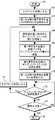
図7は、本発明による複数信号発生装置間における位相調整処理の流れを示すフローチャートである。この位相調整で問題となる点は、リンク・ケーブル92及びその周辺回路を含めた装置間通信の遅延量は既知で一定であるものの、サンプリング・クロックの周波数(サンプリング周波数)が変更されると、この一定の遅延量に相当するサンプリング・クロックのクロック数が変化することである。よって、サンプリング周波数変更時に複数の信号発生装置間の位相調整を行わないと、夫々から出力される信号の位相が変更前のサンプリング周波数では合っていても、変更後にずれるという現象が生じる。そこで、本発明では、サンプリング周波数変更時(ステップ72)には、第1又は第2信号発生装置のCPUが装置間通信の遅延量に相当するサンプリング・クロックのクロック数と位相を計算し(ステップ64)、この計算値に基いて装置間の位相調整を行う。この計算は、第1又は第2信号発生装置の一方のCPUが行うが、リンク・ケーブルを介して、この計算値の情報は両CPUで共有される。よって、サンプリング周波数変更の度に、装置間の出力信号の位相を検出して位相調整することはない。 FIG. 7 is a flowchart showing the flow of the phase adjustment process between the multiple signal generators according to the present invention. The problem with this phase adjustment is that although the delay amount of communication between devices including the link cable 92 and its peripheral circuits is known and constant, if the frequency of the sampling clock (sampling frequency) is changed, That is, the number of sampling clocks corresponding to this fixed delay amount changes. Therefore, if phase adjustment between a plurality of signal generators is not performed at the time of changing the sampling frequency, there occurs a phenomenon that even if the phase of the signal output from each is matched at the sampling frequency before the change, it is shifted after the change. Therefore, in the present invention, when the sampling frequency is changed (step 72), the CPU of the first or second signal generating device calculates the number of clocks and the phase of the sampling clock corresponding to the delay amount of the inter-device communication (step 72). 64), phase adjustment between apparatuses is performed based on the calculated value. This calculation is performed by one of the CPUs of the first or second signal generator, and information on the calculated value is shared by both CPUs via the link cable. Therefore, every time the sampling frequency is changed, the phase of the output signal between the devices is not detected and the phase is not adjusted.
上述のように、通常は信号発生装置間の位相調整を計算値に基いて行うにしても、装置の電源投入時など適当なタイミングで、回路222が実際にクロックの位相を検出して装置間の位相調整をしても良い(ステップ62)。これによって、計算値だけで位相調整し続けた場合に累積する誤差を相殺できる。この位相調整は、上述のように、第2信号発生装置内の第1サンプリング・クロック位相調整回路216がCPU236の制御に従って行う。 As described above, even if the phase adjustment between the signal generators is usually performed based on the calculated value, the circuit 222 actually detects the clock phase at an appropriate timing such as when the device is turned on. May be adjusted (step 62). As a result, errors accumulated when the phase adjustment is continued only by the calculated value can be canceled. As described above, this phase adjustment is performed by the first sampling clock phase adjustment circuit 216 in the second signal generator according to the control of the
ここで、信号発生装置の動作開始からステップ70で信号が実質的に出力されるまでは、アイドリング状態にして行うと良い。電源投入後であれば(ステップ61)、例えば電圧0Vに対応する波形データを波形メモリ128から読み出し続けるようにシーケンサが波形メモリにアドレスを供給する。また、既に動作を開始した後で、サンプリング周波数を変更した後(ステップ73)であれば、直前に出力していた電圧、例えば、0.8Vなどを維持するようにシーケンサが波形メモリにアドレスを供給する。なお、ステップ73については、サンプリング周波数変更時の出力波形の多少の乱れなどを許容できれば、サンプリング周波数変更後にアイドリング状態に入らなくても良い。 Here, from the start of the operation of the signal generator until the signal is substantially output in
ステップ66では、CPU136が第1信号発生装置の遅延回路130を制御し、ステップ64で計算した通信遅延量に相当するサンプリング・クロック数に応じて、波形データを遅延させる。上述の如く、並列波形データの組み替えにより、サンプリング・クロック単位で遅延量を調整できる。このとき遅延回路130では、通信遅延量に相当するサンプリング・クロック数の内、16で割り切れる分については、第1遅延ブロック50で遅延し、端数分について、第2遅延ブロック55で遅延する。ステップ68では、第2信号発生装置の第1及び第2シーケンス・クロック位相調整回路216及び218を用いて、サンプリング・クロックの1周期に満たない位相分について、第2信号発生装置側の波形データの位相を調整する。なお、これに代わって、第1信号発生装置の第1及び第2シーケンス・クロック位相調整回路116及び118で、第1信号発生装置側の波形データの位相を調整するようにしても良い。 In
位相調整が終わると、アイドリング状態から抜けて第1及び第2信号発生装置から実質的な信号出力を開始又は再開する(ステップ70)。予め設定したシーケンスの終了やユーザの操作により、信号出力は終了する(ステップ74)。 When the phase adjustment is completed, the system exits the idling state and starts or restarts substantial signal output from the first and second signal generators (step 70). The signal output is ended by the end of the preset sequence or the user's operation (step 74).
次に、サンプリング周波数変更に伴うもう1つの問題について説明する。第2信号発生装置200では、第1信号発生装置100から供給されたトリガ信号及びイベント信号を、回路222がシーケンス・クロック(分周クロック)に従って検出し、トリガ/イベント機能を実行する。しかし、第2信号発生装置のシーケンス・クロックの位相は、最初こそ第1信号発生装置のものと合わせるが、サンプリング周波数の変更があると、第1信号発生装置のシーケンス・クロックの位相と異なってくるので、トリガ信号とイベント信号を検出するタイミングが第1及び第2信号発生装置のシーケンス・クロック間で異なってしまう。そこで、サンプリング周波数の変更ごとに算出する通信遅延量に相当するサンプリング・クロックのクロック数から、第1信号発生装置のシーケンス・クロックに対する第2信号発生装置のシーケンス・クロックの位相遅延量を算出し、それに応じて第1信号発生装置から第2信号発生装置に供給するトリガ信号及びイベント信号(これらをタイミング信号と呼ぶ)の位相を調整する。なお、ここではシーケンス・クロックが位相遅延量ゼロから丁度1周期遅れたら、位相遅延はゼロに戻るとする。 Next, another problem associated with changing the sampling frequency will be described. In the second signal generator 200, the circuit 222 detects the trigger signal and event signal supplied from the
図8は、第2信号発生装置のシーケンス・クロックの位相遅延量と、タイミング信号の遅延量の関係を示すタイミング図である。このとき、図8(1)は第2信号発生装置のシーケンス・クロックの位相遅延量を示し、図8(2)はタイミング信号の遅延量を示す。もしシーケンス・クロックの遅延量が0度から90度の範囲(範囲A)であれば、第1信号発生装置の回路122は、タイミング信号を遅延せずに供給する。もしシーケンス・クロックの遅延量が90度から180度の範囲(範囲B)であれば、第1信号発生装置の回路122は、タイミング信号を90度遅延して供給する。もしシーケンス・クロックの遅延量が180度から270度の範囲(範囲C)であれば、第1信号発生装置の回路122は、タイミング信号を180度遅延して供給する。もしシーケンス・クロックの遅延量が270度から360度の範囲(範囲D)であれば、第1信号発生装置の回路122は、タイミング信号を270度遅延して供給する。もちろん、回路が複雑になってもよければ、第2信号発生装置のシーケンス・クロックの位相遅延量と同じだけ遅延するようにしても良い。逆に、タイミング信号検出の時間的マージンが小さくなるため、場合によるが、回路を簡単にするため、シーケンス・クロックの遅延量が0度から180度の範囲(範囲A及びB)のとき、第1信号発生装置の回路122がタイミング信号を遅延せずに供給し、シーケンス・クロックの遅延量が180度から360度の範囲(範囲C及びD)のとき、第1信号発生装置の回路122がタイミング信号を180度遅延して供給するようにしても良い。 FIG. 8 is a timing chart showing the relationship between the phase delay amount of the sequence clock of the second signal generator and the delay amount of the timing signal. At this time, FIG. 8A shows the phase delay amount of the sequence clock of the second signal generator, and FIG. 8B shows the delay amount of the timing signal. If the delay amount of the sequence clock is in the range of 0 to 90 degrees (range A), the
以上、好適な実施形態に基づき説明してきたが、当業者であれば、本発明の趣旨を沿って種々の変更が可能であろう。 Although the description has been given based on the preferred embodiments, various modifications may be made by those skilled in the art along the spirit of the present invention.
90 同軸ケーブル
92 リンク・ケーブル
100 第1信号発生装置
200 第2信号発生装置
110、210 サンプリング・クロック発振回路
114、214 サンプリング・クロック分配回路
116、216 第1サンプリング・クロック位相調整回路
118、218 第2サンプリング・クロック位相調整回路
120、220 分周回路
124、224 シーケンサ
128、228 波形メモリ
130、230 遅延回路
132、232 並直列変換回路
134、234デジタル・アナログ変換回路
122、222 トリガ/イベント信号処理・位相遅延及びクロック位相検出回路
136、236 CPU90 Coaxial cable 92
Claims (4)
Translated fromJapanese上記第1信号発生装置の上記サンプリング・クロック及び上記タイミング信号を上記第2信号発生装置に供給すると共に、上記第1及び第2信号発生装置夫々の上記中央制御手段間で情報を通信するための通信手段とを具える信号発生システムにおいて、
上記第2信号発生装置は、上記第2信号発生装置の上記サンプリング・クロック供給手段が供給する上記サンプリング・クロックの代わりとして、上記第1信号発生装置が供給する上記サンプリング・クロックを使用すると共に、上記第2信号発生装置の上記タイミング制御手段は、上記第1信号発生装置が供給する上記タイミング信号を受け、該タイミング信号を上記第2信号発生装置の上記シーケンス制御手段に供給し、
上記第1信号発生装置の上記サンプリング・クロックの周波数が変更されたときに、上記第1又は第2信号発生装置の上記中央制御手段は、上記通信手段における遅延量を上記周波数の変更後の上記サンプリング・クロックのクロック数で表した値を計算し、該クロック数で表した値に応じて上記第1信号発生装置の上記遅延手段が上記データを遅延することにより、上記第1及び第2信号発生装置で生成する上記高速データの位相関係を調整することを特徴とする信号発生システム。Sampling clock supply means for supplying a frequency-variable sampling clock, frequency dividing means for dividing the sampling clock to supply a divided clock, sequence control means for controlling the data supply sequence, and the data Waveform storage means for supplying the data in accordance with the divided clock, timing control means for supplying a timing signal for controlling the data supply timing to the sequence control means, and delay means for delaying the data in units of the sampling clock. , First and second respectively having parallel-serial conversion means for parallel-serial conversion of the data received from the delay means and outputting as high-speed data in accordance with the sampling clock, and central control means for controlling the respective means. A signal generator;
Supplying the sampling clock and timing signal of the first signal generator to the second signal generator and communicating information between the central control means of each of the first and second signal generators In a signal generation system comprising a communication means,
The second signal generator uses the sampling clock supplied by the first signal generator instead of the sampling clock supplied by the sampling clock supply means of the second signal generator, The timing control means of the second signal generator receives the timing signal supplied by the first signal generator, supplies the timing signal to the sequence control means of the second signal generator,
When the frequency of the sampling clock of the first signal generator is changed, the central control unit of the first or second signal generator changes the delay amount in the communication unit after the change of the frequency. A value represented by the number of clocks of the sampling clock is calculated,and the delay means of the first signal generator delays the data according tothe value represented by the numberof clocks,whereby the first and second signals A signal generation system characterized by adjusting a phase relationship of the high-speed data generated by the generator.
上記第1信号発生装置の上記サンプリング・クロックの周波数が変更されたときに、上記第1又は第2信号発生装置の上記中央制御手段は、上記通信手段における上記遅延量を上記周波数の変更後の上記サンプリング・クロックのクロック数及びクロック位相で表した値を計算し、上記クロック数で表した値に応じて上記第1信号発生装置の上記遅延手段が上記データを遅延すると共に、上記クロック位相で表した値に応じて上記第1又は第2信号発生装置の第1及び第2サンプリング・クロック位相調整手段が供給する上記サンプリング・クロックの位相を調整することにより、上記第1及び第2信号発生装置で生成する上記高速データの位相関係を調整することを特徴とする請求項1記載の信号発生システム。The first and second signal generators adjust the sampling clock phase adjusting means for adjusting the phase of the sampling clock supplied to the frequency dividing means, and the sampling clock supplied to the parallel-serial conversion means. A second sampling clock phase adjusting means for adjusting the phase;
When the frequency of the sampling clock of the first signal generator is changed, the central control means of the first or second signal generator changes the delay amount in the communication means after the change of the frequency. A value represented by the clock number and clock phase of the sampling clock is calculated, and the delay means of the first signal generator delays the data according tothe value represented by the clock number, andat the clock phase. The first and second signal generators are adjusted by adjusting the phase of the sampling clock supplied by the first and second sampling clock phase adjusting means of the first or second signal generator according to therepresented value. 2. The signal generation system according to claim 1, wherein the phase relationship of the high-speed data generated by the apparatus is adjusted.
上記分周クロック位相比較手段を用いて上記第1信号発生装置からの上記分周クロックと上記第2信号発生装置の上記分周クロックの位相を一致させた後に、上記第1又は第2信号発生装置の上記中央制御手段が、上記通信手段における遅延量を上記周波数の変更後の上記サンプリング・クロックの上記クロック数で表した値を計算することを特徴とする請求項1又は2記載の信号発生システム。The second signal generator further includes a divided clock phase comparing means, and the communication means supplies the divided clock of the first signal generator to the second signal generator;
The first or second signal is generated after the phase of the frequency-divided clock from the first signal generator and the frequency-divided clock of the second signal generator are matched by using the frequency-divided clock phase comparison means. 3. The signal generation according to claim 1, wherein the central control means of the apparatus calculates a value representing the delay amount in the communication means by the number of clocks of the sampling clock after the change of the frequency. system.
Priority Applications (2)
| Application Number | Priority Date | Filing Date | Title |
|---|---|---|---|
| JP2007337324AJP4474532B2 (en) | 2007-12-27 | 2007-12-27 | Signal generation system |
| US12/340,639US8483341B2 (en) | 2007-12-27 | 2008-12-19 | Signal generation system |
Applications Claiming Priority (1)
| Application Number | Priority Date | Filing Date | Title |
|---|---|---|---|
| JP2007337324AJP4474532B2 (en) | 2007-12-27 | 2007-12-27 | Signal generation system |
Publications (2)
| Publication Number | Publication Date |
|---|---|
| JP2009159468A JP2009159468A (en) | 2009-07-16 |
| JP4474532B2true JP4474532B2 (en) | 2010-06-09 |
Family
ID=40797434
Family Applications (1)
| Application Number | Title | Priority Date | Filing Date |
|---|---|---|---|
| JP2007337324AExpired - Fee RelatedJP4474532B2 (en) | 2007-12-27 | 2007-12-27 | Signal generation system |
Country Status (2)
| Country | Link |
|---|---|
| US (1) | US8483341B2 (en) |
| JP (1) | JP4474532B2 (en) |
Families Citing this family (11)
| Publication number | Priority date | Publication date | Assignee | Title |
|---|---|---|---|---|
| US8878620B2 (en)* | 2012-08-24 | 2014-11-04 | Tektronix, Inc. | Phase coherent playback in and arbitrary waveform generator |
| DE102015202505A1 (en)* | 2014-12-04 | 2016-06-09 | Rohde & Schwarz Gmbh & Co. Kg | Function generator for providing electrical signals |
| DE102015212243A1 (en)* | 2015-06-30 | 2017-01-05 | TRUMPF Hüttinger GmbH + Co. KG | Device for generating a plurality of clock or high-frequency signals |
| CN108732422B (en)* | 2017-04-14 | 2020-09-29 | 奇景光电股份有限公司 | Abnormal frequency detection method and circuit thereof |
| CN110989766A (en)* | 2018-11-16 | 2020-04-10 | 苏州普源精电科技有限公司 | A method and apparatus for constructing an arbitrary wave function |
| CN110166046B (en)* | 2019-05-20 | 2021-08-17 | 电子科技大学 | Sequential Equivalent Sampling System Based on Phase Delay |
| US11042500B1 (en)* | 2019-12-19 | 2021-06-22 | Cadence Design Systems, Inc. | Systems and methods for high-speed data transfer over a communication interface |
| US20230280780A1 (en)* | 2020-07-01 | 2023-09-07 | Zurich Instruments Ag | An arbitrary waveform generator with advanced command control |
| US12437223B2 (en) | 2021-12-15 | 2025-10-07 | Zurich Instruments Ag | Phase-accurate generation of quantum-computing control signals |
| US12000889B2 (en)* | 2022-07-05 | 2024-06-04 | Rohde & Schwarz Gmbh Co. Kg | Signal generation device, measurement device, and method |
| CN117311300B (en)* | 2023-11-29 | 2024-02-13 | 西安热工研究院有限公司 | Methods, devices and electronic equipment for dynamically adjusting sampling frequency in decentralized control systems |
Family Cites Families (8)
| Publication number | Priority date | Publication date | Assignee | Title |
|---|---|---|---|---|
| US5521949A (en)* | 1992-05-29 | 1996-05-28 | At&T Corp. | Synchronization scheme for digital communications systems transporting data at a customer-controlled rate |
| US6807509B2 (en)* | 2001-12-11 | 2004-10-19 | International Business Machines Corporation | Method and systems to measure propagation delay in semiconductor chips |
| US7533285B2 (en)* | 2004-04-22 | 2009-05-12 | Hewlett-Packard Development Company, L.P. | Synchronizing link delay measurement over serial links |
| US7289587B2 (en)* | 2004-04-22 | 2007-10-30 | Hewlett-Packard Development Company, L.P. | Repeatability over communication links |
| US20060222125A1 (en)* | 2005-03-31 | 2006-10-05 | Edwards John W Jr | Systems and methods for maintaining synchronicity during signal transmission |
| US7477712B2 (en)* | 2005-04-29 | 2009-01-13 | Hewlett-Packard Development Company, L.P. | Adaptable data path for synchronous data transfer between clock domains |
| JP4192229B2 (en) | 2006-04-21 | 2008-12-10 | テクトロニクス・インターナショナル・セールス・ゲーエムベーハー | Data generator |
| US7890684B2 (en)* | 2006-08-31 | 2011-02-15 | Standard Microsystems Corporation | Two-cycle return path clocking |
- 2007
- 2007-12-27JPJP2007337324Apatent/JP4474532B2/ennot_activeExpired - Fee Related
- 2008
- 2008-12-19USUS12/340,639patent/US8483341B2/enactiveActive
Also Published As
| Publication number | Publication date |
|---|---|
| US20090167375A1 (en) | 2009-07-02 |
| JP2009159468A (en) | 2009-07-16 |
| US8483341B2 (en) | 2013-07-09 |
Similar Documents
| Publication | Publication Date | Title |
|---|---|---|
| JP4474532B2 (en) | Signal generation system | |
| JP4893052B2 (en) | Receiver circuit and receiver circuit test method | |
| JP2008011189A (en) | Time interleave a/d conversion apparatus | |
| KR100533915B1 (en) | Clock signal selecting device and method for guaranting its clock continuity | |
| US11349491B2 (en) | Time-interleaved sampling circuits with randomized skipping | |
| CN105144587A (en) | Efficient time-interleaved analog-to-digital converter | |
| JP4279489B2 (en) | Timing generator and test apparatus | |
| JP2016052125A (en) | System for synchronizing arbitrary waveform generators, multiple awg system synchronizing method, and method for synchronizing multiple devices | |
| JP2001148690A (en) | Clock generator | |
| CN115932351B (en) | Oscilloscope cascade delay correction method, oscilloscope, terminal and medium | |
| EP3751382B1 (en) | Sequence signal generator and sequence signal generation method | |
| TWI473432B (en) | Multiphase clock divider | |
| CN117353748B (en) | Delay correction method and related equipment | |
| CN116032252B (en) | Digital-analog interface time sequence control circuit | |
| JP4192229B2 (en) | Data generator | |
| US20050248380A1 (en) | System and method for generating multiple clock signals | |
| JP4198068B2 (en) | Method and apparatus for digital frequency conversion | |
| JPH10240375A (en) | Clock non-stop switching device | |
| JP5338185B2 (en) | Acoustic signal processing device | |
| JP2008067352A (en) | Variable delay device | |
| JP6888210B2 (en) | Pulse pattern generator, error rate measurement system using it, and pulse pattern generation method | |
| JP2008147922A (en) | A/d converting device | |
| Xing et al. | Synchronization method of multiple multiplexed DACs | |
| CN116506059B (en) | Clock synchronization method and clock synchronization circuit | |
| JP2011217102A (en) | Receiver |
Legal Events
| Date | Code | Title | Description |
|---|---|---|---|
| A625 | Written request for application examination (by other person) | Free format text:JAPANESE INTERMEDIATE CODE: A625 Effective date:20090717 | |
| A977 | Report on retrieval | Free format text:JAPANESE INTERMEDIATE CODE: A971007 Effective date:20091106 | |
| A131 | Notification of reasons for refusal | Free format text:JAPANESE INTERMEDIATE CODE: A131 Effective date:20091110 | |
| A521 | Request for written amendment filed | Free format text:JAPANESE INTERMEDIATE CODE: A523 Effective date:20091130 | |
| TRDD | Decision of grant or rejection written | ||
| A01 | Written decision to grant a patent or to grant a registration (utility model) | Free format text:JAPANESE INTERMEDIATE CODE: A01 Effective date:20100209 | |
| A01 | Written decision to grant a patent or to grant a registration (utility model) | Free format text:JAPANESE INTERMEDIATE CODE: A01 | |
| A61 | First payment of annual fees (during grant procedure) | Free format text:JAPANESE INTERMEDIATE CODE: A61 Effective date:20100209 | |
| R150 | Certificate of patent or registration of utility model | Free format text:JAPANESE INTERMEDIATE CODE: R150 Ref document number:4474532 Country of ref document:JP Free format text:JAPANESE INTERMEDIATE CODE: R150 | |
| FPAY | Renewal fee payment (event date is renewal date of database) | Free format text:PAYMENT UNTIL: 20130319 Year of fee payment:3 | |
| R250 | Receipt of annual fees | Free format text:JAPANESE INTERMEDIATE CODE: R250 | |
| R250 | Receipt of annual fees | Free format text:JAPANESE INTERMEDIATE CODE: R250 | |
| R250 | Receipt of annual fees | Free format text:JAPANESE INTERMEDIATE CODE: R250 | |
| R250 | Receipt of annual fees | Free format text:JAPANESE INTERMEDIATE CODE: R250 | |
| R250 | Receipt of annual fees | Free format text:JAPANESE INTERMEDIATE CODE: R250 | |
| R250 | Receipt of annual fees | Free format text:JAPANESE INTERMEDIATE CODE: R250 | |
| LAPS | Cancellation because of no payment of annual fees |