JP4469677B2 - Semiconductor device and manufacturing method thereof - Google Patents
Semiconductor device and manufacturing method thereofDownload PDFInfo
- Publication number
- JP4469677B2 JP4469677B2JP2004227688AJP2004227688AJP4469677B2JP 4469677 B2JP4469677 B2JP 4469677B2JP 2004227688 AJP2004227688 AJP 2004227688AJP 2004227688 AJP2004227688 AJP 2004227688AJP 4469677 B2JP4469677 B2JP 4469677B2
- Authority
- JP
- Japan
- Prior art keywords
- peak
- impurity
- region
- impurity concentration
- impurity layer
- Prior art date
- Legal status (The legal status is an assumption and is not a legal conclusion. Google has not performed a legal analysis and makes no representation as to the accuracy of the status listed.)
- Expired - Lifetime
Links
Images


Classifications
- H—ELECTRICITY
- H10—SEMICONDUCTOR DEVICES; ELECTRIC SOLID-STATE DEVICES NOT OTHERWISE PROVIDED FOR
- H10D—INORGANIC ELECTRIC SEMICONDUCTOR DEVICES
- H10D62/00—Semiconductor bodies, or regions thereof, of devices having potential barriers
- H10D62/10—Shapes, relative sizes or dispositions of the regions of the semiconductor bodies; Shapes of the semiconductor bodies
- H10D62/13—Semiconductor regions connected to electrodes carrying current to be rectified, amplified or switched, e.g. source or drain regions
- H10D62/149—Source or drain regions of field-effect devices
- H10D62/151—Source or drain regions of field-effect devices of IGFETs
- H—ELECTRICITY
- H10—SEMICONDUCTOR DEVICES; ELECTRIC SOLID-STATE DEVICES NOT OTHERWISE PROVIDED FOR
- H10D—INORGANIC ELECTRIC SEMICONDUCTOR DEVICES
- H10D30/00—Field-effect transistors [FET]
- H10D30/60—Insulated-gate field-effect transistors [IGFET]
- H10D30/601—Insulated-gate field-effect transistors [IGFET] having lightly-doped drain or source extensions, e.g. LDD IGFETs or DDD IGFETs
- H—ELECTRICITY
- H10—SEMICONDUCTOR DEVICES; ELECTRIC SOLID-STATE DEVICES NOT OTHERWISE PROVIDED FOR
- H10D—INORGANIC ELECTRIC SEMICONDUCTOR DEVICES
- H10D62/00—Semiconductor bodies, or regions thereof, of devices having potential barriers
- H10D62/10—Shapes, relative sizes or dispositions of the regions of the semiconductor bodies; Shapes of the semiconductor bodies
- H10D62/17—Semiconductor regions connected to electrodes not carrying current to be rectified, amplified or switched, e.g. channel regions
- H10D62/213—Channel regions of field-effect devices
- H10D62/221—Channel regions of field-effect devices of FETs
- H10D62/235—Channel regions of field-effect devices of FETs of IGFETs
- H10D62/314—Channel regions of field-effect devices of FETs of IGFETs having vertical doping variations
- H—ELECTRICITY
- H10—SEMICONDUCTOR DEVICES; ELECTRIC SOLID-STATE DEVICES NOT OTHERWISE PROVIDED FOR
- H10D—INORGANIC ELECTRIC SEMICONDUCTOR DEVICES
- H10D30/00—Field-effect transistors [FET]
- H10D30/01—Manufacture or treatment
- H10D30/021—Manufacture or treatment of FETs having insulated gates [IGFET]
- H10D30/0223—Manufacture or treatment of FETs having insulated gates [IGFET] having source and drain regions or source and drain extensions self-aligned to sides of the gate
- H10D30/0227—Manufacture or treatment of FETs having insulated gates [IGFET] having source and drain regions or source and drain extensions self-aligned to sides of the gate having both lightly-doped source and drain extensions and source and drain regions self-aligned to the sides of the gate, e.g. lightly-doped drain [LDD] MOSFET or double-diffused drain [DDD] MOSFET
- H—ELECTRICITY
- H10—SEMICONDUCTOR DEVICES; ELECTRIC SOLID-STATE DEVICES NOT OTHERWISE PROVIDED FOR
- H10D—INORGANIC ELECTRIC SEMICONDUCTOR DEVICES
- H10D64/00—Electrodes of devices having potential barriers
- H10D64/01—Manufacture or treatment
- H10D64/021—Manufacture or treatment using multiple gate spacer layers, e.g. bilayered sidewall spacers
Landscapes
- Insulated Gate Type Field-Effect Transistor (AREA)
- Metal-Oxide And Bipolar Metal-Oxide Semiconductor Integrated Circuits (AREA)
Description
Translated fromJapanese本発明は、半導体装置の製造技術に関し、特に、ゲート長が0.1μm以下の世代のMISFET(metal insulator semiconductor field effect transistor )を有する半導体装置に適用した場合に有効な技術に関する。 The present invention relates to a manufacturing technique of a semiconductor device, and more particularly to a technique effective when applied to a semiconductor device having a generation MISFET (metal insulator semiconductor field effect transistor) having a gate length of 0.1 μm or less.
短チャネル効果を抑制するMISFETとして、例えば特許文献1には、ゲート電極下の基板不純物濃度分布に2つのピークを有するMISFETが記載されている。 As a MISFET that suppresses the short channel effect, for example,
図8は、従来のMISFET、具体的には0.1μm以下のゲート長を有する従来のpチャネル型MISFETの断面図である。図8に示す従来のMISFETの形成方法は次の通りである。 FIG. 8 is a cross-sectional view of a conventional MISFET, specifically, a conventional p-channel MISFET having a gate length of 0.1 μm or less. A method of forming the conventional MISFET shown in FIG. 8 is as follows.
まず、半導体基板1にn型ウェル2を形成した後、n型ウェル2の表面部に第1のn型不純物層9を形成すると共にn型ウェル2における第1のn型不純物層9の下側に第2のn型不純物層10を形成する。ここで、第1のn型不純物層9の深さ方向の不純物濃度分布は第1のピークを有し、第2のn型不純物層10の深さ方向の不純物濃度分布は第2のピークを有する。 First, after forming the n-
次に、半導体基板1上にゲート絶縁膜3を介してゲート電極4を形成した後、半導体基板1におけるゲート電極4の両側にp型のソース・ドレイン拡張領域(エクステンション領域)7を形成する。 Next, after forming the gate electrode 4 on the
次に、ゲート電極4の側壁上に、酸化シリコン膜5と窒化シリコン膜6との積層構造を持つ絶縁性のサイドウォールスペーサを形成した後、半導体基板1におけるゲート電極4の両側にp型のソース・ドレイン拡散領域8を形成する。 Next, an insulating sidewall spacer having a laminated structure of a
尚、第1のn型不純物層9及び第2のn型不純物層10は、ソース・ドレイン拡散領域8の接合深さよりも浅い領域に形成されている。また、第1のn型不純物層9の深さ方向の不純物濃度分布における第1のピークは、半導体基板1におけるチャネルが形成される領域(チャネル領域)よりも深くに位置する。さらに、第2のn型不純物層10の不純物濃度分布における第2のピークの不純物濃度は、第1のn型不純物層9の不純物濃度分布における第1のピークの不純物濃度よりも大きい。 The first n-
以上に述べた従来のMISFET構造、つまり、第1のn型不純物層9の不純物濃度分布における第1のピーク及び第2のn型不純物層10の不純物濃度分布における第2のピークの2つのピークを有し且つ第2のピークの不純物濃度が第1のピークの不純物濃度よりも大きいMISFET構造によると、制御可能な空乏層の幅が大きくなるので、サブスレッショルド係数を小さくすることができる。これにより、しきい値電圧の低下を防止できるため、MISFETのスイッチング速度を向上させることができる。また、以上の説明においては、pチャネル型MISFETを対象としたが、nチャネル型MISFETの場合も同様である。
しかしながら、前述の従来のMISFETにおいては、pチャネル型MISFET及びnチャネル型MISFETのいずれの場合であっても、オフリーク電流の増加に起因して半導体装置の低消費電力化を実現できないという問題がある。 However, the above-described conventional MISFET has a problem that the power consumption of the semiconductor device cannot be reduced due to an increase in off-leakage current in both cases of the p-channel MISFET and the n-channel MISFET. .
当該問題に対して、本発明は、MISFET、特に0.1μm程度以下のゲート長を有する短チャネルMISFETにおいて低消費電力化を確実に図ることを目的とする。 In order to solve this problem, an object of the present invention is to reliably reduce power consumption in a MISFET, particularly a short channel MISFET having a gate length of about 0.1 μm or less.
前記の目的を達成するために、本願発明者らが、ゲート電極下の不純物層における不純物濃度分布に第1のピーク(浅い位置)及び第2のピーク(深い位置)の2つのピークを有し且つ第2のピークの不純物濃度が第1のピークの不純物濃度よりも大きい従来のMISFETにおいてオフリーク電流が増加する原因について検討したところ、以下のような知見を得た。 In order to achieve the above object, the inventors of the present invention have two peaks of a first peak (shallow position) and a second peak (deep position) in the impurity concentration distribution in the impurity layer under the gate electrode. Further, when the cause of the increase in off-leakage current in the conventional MISFET in which the impurity concentration of the second peak is larger than the impurity concentration of the first peak was obtained, the following knowledge was obtained.
一般に、半導体装置の低消費電力化を図るためには、ゲート電極下の基板不純物濃度を上昇させてオフリーク電流を小さくすることが必要とされている。しかし、pチャネル型MISFETの場合を例として述べると、上層である第1のn型不純物層9における不純物濃度分布の第1のピーク及び下層である第2のn型不純物層10における不純物濃度分布の第2のピークの2つのピークを有し且つ第2のピークの不純物濃度が第1のピークの不純物濃度よりも大きい従来のMISFETにおいて、オフリーク電流を小さくするために、不純物濃度分布に第1のピークを有する第1のn型不純物層9の不純物濃度を上昇させると、第2のピークの不純物濃度を第1のピークの不純物濃度よりも大きくする必要があるため、不純物濃度分布に第2のピークを有する第2のn型不純物層10の不純物濃度も上昇させる必要がある。このため、第2のn型不純物層10とp型のソース・ドレイン拡散領域8との接合位置付近の不純物濃度も高くなり、その結果、動作電圧印加時に発生する電界が大きくなるので、オフリーク電流が増加して半導体装置の低消費電力化を実現することができない。nチャネル型MISFETの場合も同様である。尚、本願におけるオフリーク電流とは、ソース・ドレイン間に動作電圧が印加され且つゲート電極に電圧が印加されていないときにソース・ドレイン間に流れる電流を意味する。 In general, in order to reduce the power consumption of a semiconductor device, it is necessary to increase the substrate impurity concentration under the gate electrode to reduce the off-leak current. However, taking the case of a p-channel type MISFET as an example, the first peak of the impurity concentration distribution in the first n-
本発明は、以上の知見に基づきなされたものであって、具体的には、本発明に係る半導体装置は、半導体基板上に形成されたゲート電極と、半導体基板におけるゲート電極の両側に形成されたソース・ドレイン領域と、半導体基板におけるゲート電極の下側に形成され、ソース・ドレイン領域と異なる導電型を持つ第1の不純物層と、半導体基板における第1の不純物層の下側に形成され、ソース・ドレイン領域と異なる導電型を持つ第2の不純物層とを備え、第1の不純物層は深さ方向の不純物濃度分布に第1のピークを持つと共に、第1のピークはソース・ドレイン領域の接合深さよりも浅い領域に位置しており、第2の不純物層は深さ方向の不純物濃度分布に第2のピークを持つと共に、第2のピークは第1のピークよりも深く且つソース・ドレイン領域の接合深さよりも浅い領域に位置しており、第1のピークの不純物濃度は第2のピークの不純物濃度よりも高い。ここで、不純物濃度分布に第1のピークを持つ第1の不純物層は、エクステンション領域間のパンチスルーを防止する機能を有し、不純物濃度分布に第2のピークを持つ第2の不純物層は、ソース・ドレイン領域間のパンチスルーを防止する機能を有する。 The present invention has been made based on the above knowledge. Specifically, a semiconductor device according to the present invention is formed on a gate electrode formed on a semiconductor substrate and on both sides of the gate electrode in the semiconductor substrate. Formed on the lower side of the gate electrode in the semiconductor substrate, formed on the lower side of the first impurity layer in the semiconductor substrate, and formed on the lower side of the first impurity layer in the semiconductor substrate. And a second impurity layer having a conductivity type different from that of the source / drain region, the first impurity layer has a first peak in the impurity concentration distribution in the depth direction, and the first peak is the source / drain region. The second impurity layer has a second peak in the impurity concentration distribution in the depth direction, and the second peak is deeper than the first peak and is located in a region shallower than the junction depth of the region. Located in a region shallower than the junction depth of the scan and drain regions, the impurity concentration of the first peak is higher than the impurity concentration of the second peak. Here, the first impurity layer having the first peak in the impurity concentration distribution has a function of preventing punch-through between the extension regions, and the second impurity layer having the second peak in the impurity concentration distribution is And has a function of preventing punch-through between the source and drain regions.
本発明の半導体装置によると、ゲート電極下側の半導体基板に形成された第1の不純物層の不純物濃度分布における第1のピークの不純物濃度を、第1の不純物層の下側に形成された第2の不純物層の不純物濃度分布における第2のピークの不純物濃度よりも高くするため、次のような効果が得られる。すなわち、オフリーク電流を小さくするために、不純物濃度分布に第1のピークを有する第1の不純物層の不純物濃度を上昇させた場合にも、従来の半導体装置と異なり第2のピークの不純物濃度を第1のピークの不純物濃度よりも大きくする必要がないため、不純物濃度分布に第2のピークを有する第2の不純物層の不純物濃度を上昇させる必要がない。このため、第2の不純物層の不純物濃度を低く保つことができるので、閾値電圧が同等で且つ第2のピークの不純物濃度が第1のピークの不純物濃度よりも高い従来の半導体装置と比較して、ソース・ドレイン領域と該ソース・ドレイン領域の反対導電型を持つ第2の不純物層との接合位置付近の不純物濃度が小さくなる。その結果、動作電圧印加時に発生する電界が小さくなるので、オフリーク電流が減少し、それにより半導体装置の低消費電力化を実現することができる。 According to the semiconductor device of the present invention, the first peak impurity concentration in the impurity concentration distribution of the first impurity layer formed in the semiconductor substrate below the gate electrode is formed below the first impurity layer. In order to make the concentration higher than the impurity concentration of the second peak in the impurity concentration distribution of the second impurity layer, the following effects can be obtained. That is, even when the impurity concentration of the first impurity layer having the first peak in the impurity concentration distribution is increased in order to reduce the off-leakage current, the impurity concentration of the second peak is different from the conventional semiconductor device. Since it is not necessary to increase the impurity concentration of the first peak, it is not necessary to increase the impurity concentration of the second impurity layer having the second peak in the impurity concentration distribution. For this reason, since the impurity concentration of the second impurity layer can be kept low, the threshold voltage is equivalent and the impurity concentration of the second peak is higher than the impurity concentration of the first peak compared to the conventional semiconductor device. Thus, the impurity concentration in the vicinity of the junction position between the source / drain region and the second impurity layer having the opposite conductivity type of the source / drain region is reduced. As a result, the electric field generated when the operating voltage is applied is reduced, so that the off-leakage current is reduced, whereby the power consumption of the semiconductor device can be reduced.
本発明の半導体装置において、第1のピークが、半導体基板におけるチャネルが形成される領域よりも深くに位置すると、前述の効果を確実に得ることができる。 In the semiconductor device of the present invention, when the first peak is located deeper than the region where the channel is formed in the semiconductor substrate, the above-described effect can be reliably obtained.
本発明に係る第1の半導体装置の製造方法は、半導体基板の表面部に第1導電型の第1の不純物層を形成する第1の工程と、第1の工程よりも後に、半導体基板上にゲート電極を形成する第2の工程と、ゲート電極をマスクとして半導体基板に第2導電型の不純物を導入することにより、エクステンション領域を形成する第3の工程と、第3の工程よりも後に、ゲート電極をマスクとして半導体基板に第1導電型の不純物を導入することにより、半導体基板におけるエクステンション領域及び第1の不純物層の下側に第2の不純物層を形成する第4の工程と、第4の工程よりも後に、ゲート電極の側壁上に絶縁性サイドウォールを形成する第5の工程と、ゲート電極及び絶縁性サイドウォールをマスクとして半導体基板に第2導電型の不純物を導入することにより、ソース・ドレイン領域を形成する第6の工程とを備え、第1の不純物層は深さ方向の不純物濃度分布に第1のピークを持つと共に、第1のピークはソース・ドレイン領域の接合深さよりも浅い領域に位置しており、第2の不純物層は深さ方向の不純物濃度分布に第2のピークを持つと共に、第2のピークは第1のピークよりも深く且つソース・ドレイン領域の接合深さよりも浅い領域に位置しており、第1のピークの不純物濃度は第2のピークの不純物濃度よりも高い。 A first method for manufacturing a semiconductor device according to the present invention includes a first step of forming a first impurity layer of a first conductivity type on a surface portion of a semiconductor substrate, and a semiconductor substrate after the first step. A second step of forming a gate electrode on the substrate, a third step of forming an extension region by introducing a second conductivity type impurity into the semiconductor substrate using the gate electrode as a mask, and a step after the third step. A fourth step of forming a second impurity layer below the extension region and the first impurity layer in the semiconductor substrate by introducing a first conductivity type impurity into the semiconductor substrate using the gate electrode as a mask; After the fourth step, a fifth step of forming an insulating sidewall on the side wall of the gate electrode, and a second conductivity type impurity in the semiconductor substrate using the gate electrode and the insulating sidewall as a mask The first impurity layer has a first peak in the impurity concentration distribution in the depth direction, and the first peak is the source / drain region. The second impurity layer has a second peak in the impurity concentration distribution in the depth direction, the second peak is deeper than the first peak, and is located in a region shallower than the junction depth of the region. It is located in a region shallower than the junction depth of the drain region, and the impurity concentration of the first peak is higher than the impurity concentration of the second peak.
本発明に係る第2の半導体装置の製造方法は、半導体基板の表面部に第1導電型の第1の不純物層を形成すると共に半導体基板における第1の不純物層の下側に第2の不純物層を形成する第1の工程と、第1の工程よりも後に、半導体基板上にゲート電極を形成する第2の工程と、ゲート電極をマスクとして半導体基板に第2導電型の不純物を導入することにより、エクステンション領域を形成する第3の工程と、第3の工程よりも後に、ゲート電極の側壁上に絶縁性サイドウォールを形成する第4の工程と、ゲート電極及び絶縁性サイドウォールをマスクとして半導体基板に第2導電型の不純物を導入することにより、ソース・ドレイン領域を形成する第5の工程とを備え、第1の不純物層は深さ方向の不純物濃度分布に第1のピークを持つと共に、第1のピークはソース・ドレイン領域の接合深さよりも浅い領域に位置しており、第2の不純物層は深さ方向の不純物濃度分布に第2のピークを持つと共に、第2のピークは第1のピークよりも深く且つソース・ドレイン領域の接合深さよりも浅い領域に位置しており、第1のピークの不純物濃度は第2のピークの不純物濃度よりも高い。尚、第2の半導体装置の製造方法において、第1の不純物層を形成した後に第2の不純物層を形成してもよいし、又は第1の不純物層を形成する前に第2の不純物層を形成してもよい。 According to the second method of manufacturing the semiconductor device of the present invention, the first impurity layer of the first conductivity type is formed on the surface portion of the semiconductor substrate, and the second impurity is formed below the first impurity layer in the semiconductor substrate. A first step of forming a layer; a second step of forming a gate electrode on the semiconductor substrate after the first step; and introducing a second conductivity type impurity into the semiconductor substrate using the gate electrode as a mask. Accordingly, the third step of forming the extension region, the fourth step of forming the insulating sidewall on the side wall of the gate electrode after the third step, and masking the gate electrode and the insulating sidewall And a fifth step of forming source / drain regions by introducing a second conductivity type impurity into the semiconductor substrate, wherein the first impurity layer has a first peak in the impurity concentration distribution in the depth direction. Holding In addition, the first peak is located in a region shallower than the junction depth of the source / drain region, the second impurity layer has the second peak in the impurity concentration distribution in the depth direction, and the second peak. Is located in a region deeper than the first peak and shallower than the junction depth of the source / drain region, and the impurity concentration of the first peak is higher than the impurity concentration of the second peak. In the second semiconductor device manufacturing method, the second impurity layer may be formed after the first impurity layer is formed, or the second impurity layer may be formed before the first impurity layer is formed. May be formed.
すなわち、第1及び第2の半導体装置の製造方法はいずれも前述の本発明の半導体装置を製造するための方法であるので、前述の本発明の半導体装置と同様の効果が得られる。 That is, since both the first and second semiconductor device manufacturing methods are methods for manufacturing the above-described semiconductor device of the present invention, the same effects as those of the above-described semiconductor device of the present invention can be obtained.
本発明によると、従来の半導体装置と異なりゲート電極下側の半導体基板に形成された第1の不純物層の不純物濃度分布における第1のピークの不純物濃度を、第1の不純物層の下側に形成された第2の不純物層の不純物濃度分布における第2のピークの不純物濃度よりも高く設定している。このため、オフリーク電流を小さくするために、第1の不純物層の不純物濃度を上昇させた場合にも第2の不純物層を上昇させる必要がないので、第2の不純物層の不純物濃度を低く保つことができる。従って、ソース・ドレイン領域と該ソース・ドレイン領域の反対導電型を持つ第2の不純物層との接合位置付近の不純物濃度が小さくなる結果、動作電圧印加時に発生する電界が小さくなるので、オフリーク電流が減少し、それにより半導体装置の低消費電力化を実現することができる。特に、0.1μm程度以下のゲート長を有するMISFETつまり短チャネルMISFETにおいて従来技術と比べてさらなる消費電力の低下を図ることができる。 According to the present invention, unlike the conventional semiconductor device, the first peak impurity concentration in the impurity concentration distribution of the first impurity layer formed on the semiconductor substrate below the gate electrode is set below the first impurity layer. It is set higher than the impurity concentration of the second peak in the impurity concentration distribution of the formed second impurity layer. For this reason, since it is not necessary to raise the second impurity layer even when the impurity concentration of the first impurity layer is increased in order to reduce the off-leakage current, the impurity concentration of the second impurity layer is kept low. be able to. Therefore, the impurity concentration in the vicinity of the junction position between the source / drain region and the second impurity layer having the opposite conductivity type of the source / drain region is reduced, so that the electric field generated when the operating voltage is applied is reduced. As a result, the power consumption of the semiconductor device can be reduced. In particular, in a MISFET having a gate length of about 0.1 μm or less, that is, a short channel MISFET, the power consumption can be further reduced as compared with the prior art.
(第1の実施形態)
以下、本発明の第1の実施形態に係る半導体装置及びその製造方法について図面を参照しながら説明する。(First embodiment)
Hereinafter, a semiconductor device and a manufacturing method thereof according to a first embodiment of the present invention will be described with reference to the drawings.
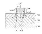
図1は、第1の実施形態に係る半導体装置、具体的には0.1μm以下のゲート長を有するpチャネル型MOS(metal oxide semiconductor )デバイスの断面図である。 FIG. 1 is a cross-sectional view of the semiconductor device according to the first embodiment, specifically, a p-channel MOS (metal oxide semiconductor) device having a gate length of 0.1 μm or less.
図1に示すように、例えばp型の単結晶シリコンからなる基板101におけるpチャネル型MISFET形成領域にn型のウェル102が形成されている。また、基板101におけるpチャネル型MISFET形成領域の上にはゲート絶縁膜103を介して例えばp型の多結晶シリコン膜からなるゲート電極104が形成されている。ゲート電極104の側壁上には、例えば酸化シリコン膜105と窒化シリコン膜106との積層構造を持つ絶縁性のサイドウォールスペーサが形成されている。ウェル102の表面部におけるゲート電極104の側部の下側にはp型のソース・ドレイン拡張領域(エクステンション領域)107が形成されている。また、ウェル102におけるゲート電極104から見てエクステンション領域107の外側には、エクステンション領域107の接合深さ(例えば基板表面から0.04μm程度の深さ)よりも深い位置に接合深さ(例えば基板表面から0.11μm程度の深さ)を有するソース・ドレイン拡散領域108が形成されている。また、ウェル102の表面部におけるゲート電極104の下側には、例えばn型の第1の不純物層109がエクステンション領域107に挟まれるように形成されている。さらに、ウェル102におけるエクステンション領域107及び第1の不純物層109の下側には、ポケット領域となるn型の第2の不純物層110がソース・ドレイン拡散領域108と接するように形成されている。尚、本実施形態においては、第1の不純物層109及び第2の不純物層110はいずれも、ソース・ドレイン拡散領域108の接合深さよりも浅い領域に形成されている。 As shown in FIG. 1, an n-
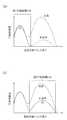
以下、図1に示す本実施形態のpチャネル型MISFETの諸特性について図2(a)及び(b)を参照しながら説明する。図2(a)は、図1のa−a’線における不純物濃度分布を示し、図2(b)は、図1のb−b’線における不純物濃度分布を示している。尚、図2(a)及び(b)においては、比較のため、従来のpチャネル型MISFETの不純物濃度分布も合わせて示している。 Hereinafter, various characteristics of the p-channel MISFET of this embodiment shown in FIG. 1 will be described with reference to FIGS. 2 (a) and 2 (b). 2A shows the impurity concentration distribution along the line a-a ′ in FIG. 1, and FIG. 2B shows the impurity concentration distribution along the line b-b ′ in FIG. 1. 2A and 2B also show the impurity concentration distribution of a conventional p-channel MISFET for comparison.
図2(a)に示すように、第1の不純物層109は、深さ方向の不純物濃度分布に第1のピークP1(不純物濃度は例えば5×10¹⁸(ions/cm3)以上で且つ8×1018(ions/cm3)以下)を有している。ここで、第1のピークP1は、基板表面からの深さが5nm以上で且つ15nm以下の領域に位置している。すなわち、第1のピークP1は、基板101におけるチャネルが形成される領域(基板表面からの深さが例えば2nm程度以下の領域)よりも深く且つソース・ドレイン拡散領域108の接合深さ(例えば基板表面から0.1μm程度の深さ)よりも浅い領域に位置する。As shown in FIG. 2A, the
また、図2(b)に示すように、第2の不純物層110は、深さ方向の不純物濃度分布に第2のピークP2(不純物濃度は例えば1×10¹⁸(ions/cm3)以上で且つ5×1018(ions/cm3)未満)を有している。ここで、第2のピークP2は、基板表面からの深さが20nm以上で且つ90nm以下の領域に位置している。すなわち、第2のピークP2は、第1のピークP1よりも深く且つソース・ドレイン拡散領域108の接合深さ(例えば基板表面から0.1μm程度の深さ)よりも浅い領域に位置する。Further, as shown in FIG. 2B, the
また、図2(a)及び(b)に示すように、本実施形態のpチャネル型MISFETにおいては、第1のピークP1の不純物濃度は第2のピークP2の不純物濃度よりも高いのに対して、従来のpチャネル型MISFETにおいては、浅い位置のピーク(本実施形態の第1のピークP1に相当する)の不純物濃度は、深い位置のピーク(本実施形態の第2のピークP2に相当する)の不純物濃度よりも低い。 As shown in FIGS. 2A and 2B, in the p-channel MISFET of this embodiment, the impurity concentration of the first peak P1 is higher than the impurity concentration of the second peak P2. In the conventional p-channel MISFET, the impurity concentration at the shallow peak (corresponding to the first peak P1 in the present embodiment) is equivalent to the deep peak (corresponding to the second peak P2 in the present embodiment). Lower) than the impurity concentration.
以上のような特徴を有する本実施形態の半導体装置によると、従来の半導体装置と異なりゲート電極104の下側の基板101に形成された第1の不純物層109の不純物濃度分布における第1のピークP1の不純物濃度を、第1の不純物層109の下側に形成された第2の不純物層110の不純物濃度分布における第2のピークP2の不純物濃度よりも高く設定している。このため、オフリーク電流を小さくするために、第1の不純物層109の不純物濃度を上昇させた場合にも、従来の半導体装置と異なり第2のピークP2の不純物濃度を第1のピークP1の不純物濃度よりも大きくする必要がないため、第2の不純物層110の不純物濃度を上昇させる必要がない。従って、第2の不純物層110の不純物濃度を低く保つことができるので、閾値電圧が同等で且つ第2のピークの不純物濃度が第1のピークの不純物濃度よりも高い従来の半導体装置と比較して、ソース・ドレイン領域108と該ソース・ドレイン領域108の反対導電型を持つ第2の不純物層110との接合位置付近の不純物濃度が小さくなる。その結果、動作電圧印加時に発生する電界が小さくなるので、オフリーク電流が減少し、それにより半導体装置の低消費電力化を実現することができる。 According to the semiconductor device of this embodiment having the above-described features, unlike the conventional semiconductor device, the first peak in the impurity concentration distribution of the
図3は、本実施形態のpチャネル型MISFETにおけるオフリーク電流と閾値電圧との関係を、従来のpチャネル型MISFETにおけるオフリーク電流と閾値電圧との関係と比較して示している。 FIG. 3 shows the relationship between the off-leakage current and the threshold voltage in the p-channel type MISFET of this embodiment in comparison with the relationship between the off-leakage current and the threshold voltage in the conventional p-channel type MISFET.
図3に示すように、本実施形態によると、従来の半導体装置と比較して、オフリーク電流を減少させて半導体装置の消費電力を低減させることができる。 As shown in FIG. 3, according to the present embodiment, the power consumption of the semiconductor device can be reduced by reducing the off-leak current as compared with the conventional semiconductor device.
以下、図1に示す本実施形態のpチャネル型MISFETの製造方法について図面を参照しながら説明する。 A method for manufacturing the p-channel MISFET of this embodiment shown in FIG. 1 will be described below with reference to the drawings.
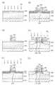
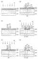
図4(a)〜(f)は、第1の実施形態に係る半導体装置の製造方法の各工程を示す断面図である。 4A to 4F are cross-sectional views illustrating respective steps of the method for manufacturing the semiconductor device according to the first embodiment.
まず、図4(a)に示すように、例えばp型の単結晶シリコンからなる基板101を用意して、基板101のpチャネル型MISFET形成領域に例えばn型のウェル102を形成するために、n型不純物、例えばリン(P)を複数回に亘って異なる注入エネルギーで基板101にイオン注入する。ここで、Pのイオン注入条件は、注入エネルギーが例えば500keV及び200keVであり、ドーズ量が例えば1×1013cm-2(一定)である。First, as shown in FIG. 4A, a
続いて、基板101のpチャネル型MISFET形成領域にn型不純物、例えばヒ素(As)をイオン注入し、それによって、深さ方向の不純物濃度分布に第1のピークP1を有する例えばn型の第1の不純物層109を形成する。ここで、Asのイオン注入条件は、注入エネルギーが例えば50eVであり、ドーズ量が例えば5×1012cm-2である。第1の不純物層109は、ソースドレイン拡張領域(エクステンション領域)107(図4(c)参照)間のパンチスルーを防止する機能を有する。また、第1のピークP1は、基板表面からの深さが例えば5nm以上で且つ15nm以下の領域に位置し、第1のピークP1の不純物濃度は例えば5×10¹⁸(ions/cm3)以上で且つ8×1018(ions/cm3)以下である。Subsequently, an n-type impurity, for example, arsenic (As) is ion-implanted into the p-channel MISFET formation region of the
次に、図4(b)に示すように、基板101に対して熱酸化を行なって、基板101の表面上に例えば厚さ2nm程度のゲート絶縁膜103を形成した後、例えば厚さ200nm程度のp型の多結晶シリコン膜を例えばCVD(chemical vapor deposition )法により基板101上に堆積する。次に、ゲート電極形成領域を覆うレジストパターン(図示省略)をマスクとして、前記の多結晶シリコン膜に対してエッチングを行なって、基板101のpチャネル型MISFET形成領域の上にゲート絶縁膜103を介して、p型多結晶シリコン膜から構成され且つ0.1μm程度のゲート長を有するゲート電極104を形成する。 Next, as shown in FIG. 4B, the
次に、図4(c)に示すように、pチャネル型MISFETのゲート電極104をマスクとして、n型のウェル102にp型不純物、例えばフッ化ボロン(BF2)をイオン注入し、それによってpチャネル型MISFETのソース・ドレイン拡張領域(エクステンション領域)107を形成する。ここで、BF2のイオン注入条件は、注入エネルギーが例えば3keVであり、ドーズ量が例えば1×1015cm-2である。また、エクステンション領域107の接合深さは例えば0.04μm程度である。Next, as shown in FIG. 4C, a p-type impurity, for example, boron fluoride (BF2 ) is ion-implanted into the n-type well 102 using the
続いて、pチャネル型MISFETのゲート電極104をマスクとして、n型ウェル102にn型不純物、例えばヒ素(As)を基板表面の法線方向に対して例えば10〜25°程度の角度でイオン注入し、それによって、n型ウェル102におけるエクステンション領域107及び第1の不純物層109の下側に、pチャネル型MISFETのポケット領域となる第2の不純物層110を形成する。ここで、Asのイオン注入条件は、注入エネルギーが例えば80keVであり、ドーズ量が例えば1×1013cm-2である。第2の不純物層110は、ソース・ドレイン拡散領域108(図4(e)参照)間のパンチスルーを防止する機能を有する。また、第2のピークP2は、基板表面からの深さが例えば20nm以上で且つ90nm以下の領域に位置し、第2のピークP2の不純物濃度は例えば1×10¹⁸(ions/cm3)以上で且つ5×1018(ions/cm3)未満である。すなわち、第2の不純物層110の第2のピークP2の基板101の表面からの深さは、第1のn型不純物層109の第1のピークP1の基板101の表面からの深さよりも相対的に大きく、第2の不純物層110の第2のピークP2の不純物濃度は、第1のn型不純物層109の第1のピークP1の不純物濃度よりも低い。尚、本実施形態では、エクステンション領域107の接合深さと、第1のn型不純物層109と第2の不純物層110との境界の深さとはほぼ同程度である。Subsequently, using the
次に、図4(d)に示すように、基板101上に例えば酸化シリコン膜105及び窒化シリコン膜106をCVD法によって順次堆積した後、窒化シリコン膜106に対して例えばRIE(reactive ion etching)法によって異方性エッチングを行ない、その後、酸化シリコン膜105に対してエッチングを行なう。これにより、pチャネル型MISFETのゲート電極104の各側壁上に、酸化シリコン膜105及び窒化シリコン膜106からなるサイドウォールスペーサが形成される。 Next, as illustrated in FIG. 4D, for example, a
次に、図4(e)に示すように、pチャネル型MISFETのゲート電極104及びサイドウォールスペーサ(酸化シリコン膜105及び窒化シリコン膜106)をマスクとして、n型のウェル102にp型不純物、例えばBF2をイオン注入し、それによって、接合深さが第2の不純物層110の第2のピークP2よりも深くに位置するソース・ドレイン拡散領域108を形成する。ここで、BF2のイオン注入条件は、注入エネルギーが例えば25keVであり、ドーズ量が例えば2×1015cm-2である。また、ソース・ドレイン拡散領域108の接合深さは例えば0.1μm程度である。Next, as shown in FIG. 4E, a p-type impurity is added to the n-type well 102 using the
以上のような工程によって、図4(f)に示すように、pチャネル型MISFETが形成される。 Through the above process, a p-channel MISFET is formed as shown in FIG.
尚、第1の実施形態において、pチャネル型MISFETを例として説明したが、nチャネル型MISFETについても同様である。 In the first embodiment, the p-channel type MISFET has been described as an example, but the same applies to the n-channel type MISFET.
また、第1の実施形態において、第1の不純物層109の深さ方向の不純物濃度分布における第1のピークP1は、基板101におけるチャネルが形成される領域よりも深くに位置することが好ましい。このようにすると、前述のオフリーク電流の低減による半導体装置の低消費電力化の効果が確実に得られる。 In the first embodiment, the first peak P1 in the impurity concentration distribution in the depth direction of the
また、第1の実施形態において、0.1μm程度以下のゲート長を有するMISFET、つまり短チャネルMISFETであると、従来技術と比べて消費電力の低減を顕著に図ることができる。 Further, in the first embodiment, a MISFET having a gate length of about 0.1 μm or less, that is, a short channel MISFET, can significantly reduce power consumption as compared with the prior art.
(第2の実施形態)
以下、本発明の第2の実施形態に係る半導体装置及びその製造方法について図面を参照しながら説明する。(Second Embodiment)
Hereinafter, a semiconductor device and a manufacturing method thereof according to the second embodiment of the present invention will be described with reference to the drawings.
図5は、第2の実施形態に係る半導体装置、具体的には0.1μm以下のゲート長を有するpチャネル型MOSデバイスの断面図である。 FIG. 5 is a cross-sectional view of the semiconductor device according to the second embodiment, specifically, a p-channel MOS device having a gate length of 0.1 μm or less.
図5に示すように、例えばp型の単結晶シリコンからなる基板201におけるpチャネル型MISFET形成領域に例えばn型のウェル202が形成されている。また、基板201におけるpチャネル型MISFET形成領域の上にはゲート絶縁膜203を介して例えばp型の多結晶シリコン膜からなるゲート電極204が形成されている。ゲート電極204の側壁上には、例えば酸化シリコン膜205と窒化シリコン膜206との積層構造を持つ絶縁性のサイドウォールスペーサが形成されている。ウェル202の表面部におけるゲート電極204の側部の下側には例えばp型のソース・ドレイン拡張領域(エクステンション領域)207が形成されている。また、ウェル202におけるゲート電極204から見てエクステンション領域207の外側には、エクステンション領域207の接合深さ(例えば基板表面から0.04μm程度の深さ)よりも深い位置に接合深さ(例えば基板表面から0.1μm程度の深さ)を有するソース・ドレイン拡散領域208が形成されている。また、ウェル202の表面部におけるゲート電極204の下側には、例えばn型の第1の不純物層209がエクステンション領域207に挟まれるように形成されている。さらに、ウェル202におけるエクステンション領域207及び第1の不純物層209の下側には、例えばn型の第2の不純物層210がソース・ドレイン拡散領域208に挟まれるように形成されている。尚、本実施形態においては、第1の不純物層209及び第2の不純物層210はいずれも、ソース・ドレイン拡散領域208の接合深さよりも浅い領域に形成されている。 As shown in FIG. 5, for example, an n-
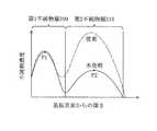
以下、図5に示す本実施形態のpチャネル型MISFETの諸特性について図6を参照しながら説明する。図6は、図5のc−c’線における不純物濃度分布を示している。尚、図6においては、比較のため、従来のpチャネル型MISFETの不純物濃度分布も合わせて示している。 Hereinafter, various characteristics of the p-channel type MISFET of this embodiment shown in FIG. 5 will be described with reference to FIG. FIG. 6 shows an impurity concentration distribution along the c-c ′ line in FIG. 5. For comparison, FIG. 6 also shows the impurity concentration distribution of a conventional p-channel MISFET.
図6に示すように、第1の不純物層209は、深さ方向の不純物濃度分布に第1のピークP1(不純物濃度は例えば5×10¹⁸(ions/cm3)以上で且つ8×1018(ions/cm3)以下)を有している。ここで、第1のピークP1は、基板表面からの深さが5nm以上で且つ15nm以下の領域に位置している。すなわち、第1のピークP1は、基板201におけるチャネルが形成される領域(基板表面からの深さが例えば2nm程度以下の領域)よりも深く且つソース・ドレイン拡散領域208の接合深さ(例えば基板表面から0.1μm程度の深さ)よりも浅い領域に位置する。As shown in FIG. 6, the
また、図6に示すように、第2の不純物層210は、深さ方向の不純物濃度分布に第2のピークP2(不純物濃度は例えば1×10¹⁸(ions/cm3)以上で且つ5×1018(ions/cm3)未満)を有している。ここで、第2のピークP2は、基板表面からの深さが20nm以上で且つ90nm以下の領域に位置している。すなわち、第2のピークP2は、第1のピークP1よりも深く且つソース・ドレイン拡散領域208の接合深さ(例えば基板表面から0.1μm程度の深さ)よりも浅い領域に位置する。As shown in FIG. 6, the
また、図6に示すように、本実施形態のpチャネル型MISFETにおいては、第1のピークP1の不純物濃度は第2のピークP2の不純物濃度よりも高いのに対して、従来のpチャネル型MISFETにおいては、浅い位置のピーク(本実施形態の第1のピークP1に相当する)の不純物濃度は、深い位置のピーク(本実施形態の第2のピークP2に相当する)の不純物濃度よりも低い。 Further, as shown in FIG. 6, in the p-channel type MISFET of this embodiment, the impurity concentration of the first peak P1 is higher than the impurity concentration of the second peak P2, whereas the conventional p-channel type MISFET. In the MISFET, the impurity concentration at the shallow peak (corresponding to the first peak P1 in the present embodiment) is higher than the impurity concentration at the deep peak (corresponding to the second peak P2 in the present embodiment). Low.
以上のような特徴を有する本実施形態の半導体装置によると、従来の半導体装置と異なりゲート電極204の下側の基板201に形成された第1の不純物層209の不純物濃度分布における第1のピークP1の不純物濃度を、第1の不純物層209の下側に形成された第2の不純物層210の不純物濃度分布における第2のピークP2の不純物濃度よりも高く設定している。このため、オフリーク電流を小さくするために、第1の不純物層209の不純物濃度を上昇させた場合にも、従来の半導体装置と異なり第2のピークP2の不純物濃度を第1のピークP1の不純物濃度よりも大きくする必要がないため、第2の不純物層210の不純物濃度を上昇させる必要がない。従って、第2の不純物層210の不純物濃度を低く保つことができるので、閾値電圧が同等で且つ第2のピークの不純物濃度が第1のピークの不純物濃度よりも高い従来の半導体装置と比較して、ソース・ドレイン領域208と該ソース・ドレイン領域208の反対導電型を持つ第2の不純物層210との接合位置付近の不純物濃度が小さくなる。その結果、動作電圧印加時に発生する電界が小さくなるので、オフリーク電流が減少し、それにより半導体装置の低消費電力化を実現することができる。 According to the semiconductor device of this embodiment having the above-described features, unlike the conventional semiconductor device, the first peak in the impurity concentration distribution of the
以下、図5に示す本実施形態のpチャネル型MISFETの製造方法について図面を参照しながら説明する。 Hereinafter, a method of manufacturing the p-channel MISFET of this embodiment shown in FIG. 5 will be described with reference to the drawings.
図7(a)〜(f)は、第2の実施形態に係る半導体装置の製造方法の各工程を示す断面図である。 7A to 7F are cross-sectional views illustrating respective steps of the method for manufacturing the semiconductor device according to the second embodiment.
まず、図7(a)に示すように、例えばp型の単結晶シリコンからなる基板201を用意して、基板201のpチャネル型MISFET形成領域に例えばn型のウェル202を形成するために、n型不純物、例えばリン(P)を複数回に亘って異なる注入エネルギーで基板201にイオン注入する。ここで、Pのイオン注入条件は、注入エネルギーが例えば500keV及び200keVであり、ドーズ量が例えば1×1013cm-2(一定)である。First, as shown in FIG. 7A, a
続いて、基板201のpチャネル型MISFET形成領域にn型不純物、例えばヒ素(As)をイオン注入し、それによって、深さ方向の不純物濃度分布に第1のピークP1を有する例えばn型の第1の不純物層209を形成する。ここで、Asのイオン注入条件は、注入エネルギーが例えば50eVであり、ドーズ量が例えば5×1012cm-2である。第1の不純物層209は、ソースドレイン拡張領域(エクステンション領域)207(図7(c)参照)間のパンチスルーを防止する機能を有する。また、第1のピークP1は、基板表面からの深さが例えば5nm以上で且つ15nm以下の領域に位置し、第1のピークP1の不純物濃度は例えば5×10¹⁸(ions/cm3)以上で且つ8×1018(ions/cm3)以下である。Subsequently, an n-type impurity, such as arsenic (As), is ion-implanted into the p-channel MISFET formation region of the
続いて、n型ウェル202にn型不純物、例えばヒ素(As)をイオン注入し、それによって、n型ウェル202における第1の不純物層209の下側に第2の不純物層210を形成する。ここで、Asのイオン注入条件は、注入エネルギーが例えば80keVであり、ドーズ量が例えば1×1013cm-2である。第2の不純物層210は、ソース・ドレイン拡散領域208(図7(e)参照)間のパンチスルーを防止する機能を有する。また、第2のピークP2は、基板表面からの深さが例えば20nm以上で且つ90nm以下の領域に位置し、第2のピークP2の不純物濃度は例えば1×10¹⁸(ions/cm3)以上で且つ5×1018(ions/cm3)未満である。すなわち、第2の不純物層210の第2のピークP2の基板201の表面からの深さは、第1のn型不純物層209の第1のピークP1の基板201の表面からの深さよりも相対的に大きく、第2の不純物層210の第2のピークP2の不純物濃度は、第1のn型不純物層209の第1のピークP1の不純物濃度よりも低い。Subsequently, an n-type impurity such as arsenic (As) is ion-implanted into the n-
尚、本実施形態において、第1の不純物層209を形成する前に第2の不純物層210を形成してもよい。 In the present embodiment, the
次に、図7(b)に示すように、基板201に対して熱酸化を行なって、基板201の表面上に例えば厚さ2nm程度のゲート絶縁膜203を形成した後、例えば厚さ200nm程度のp型の多結晶シリコン膜を例えばCVD法により基板201上に堆積する。次に、ゲート電極形成領域を覆うレジストパターン(図示省略)をマスクとして、前記の多結晶シリコン膜に対してエッチングを行なって、基板201のpチャネル型MISFET形成領域の上にゲート絶縁膜203を介して、p型多結晶シリコン膜から構成され且つ0.1μm程度のゲート長を有するゲート電極204を形成する。 Next, as shown in FIG. 7B, the
次に、図7(c)に示すように、pチャネル型MISFETのゲート電極204をマスクとして、n型のウェル202にp型不純物、例えばフッ化ボロン(BF2)をイオン注入し、それによってpチャネル型MISFETのソース・ドレイン拡張領域(エクステンション領域)207を形成する。ここで、BF2のイオン注入条件は、注入エネルギーが例えば3keVであり、ドーズ量が例えば1×1015cm-2である。また、エクステンション領域207の接合深さは例えば0.04μm程度である。尚、本実施形態では、エクステンション領域207の接合深さと、第1のn型不純物層209と第2の不純物層210との境界の深さとはほぼ同程度である。Next, as shown in FIG. 7C, a p-type impurity, for example, boron fluoride (BF2 ) is ion-implanted into the n-type well 202 using the
次に、図7(d)に示すように、基板201上に例えば酸化シリコン膜205及び窒化シリコン膜206をCVD法によって順次堆積した後、窒化シリコン膜206に対して例えばRIE法によって異方性エッチングを行ない、その後、酸化シリコン膜205に対してエッチングを行なう。これにより、pチャネル型MISFETのゲート電極204の各側壁上に、酸化シリコン膜205及び窒化シリコン膜206からなるサイドウォールスペーサが形成される。 Next, as shown in FIG. 7D, for example, a
次に、図7(e)に示すように、pチャネル型MISFETのゲート電極204及びサイドウォールスペーサ(酸化シリコン膜205及び窒化シリコン膜206)をマスクとして、n型のウェル202にp型不純物、例えばBF2をイオン注入し、それによって、接合深さが第2の不純物層210の第2のピークP2よりも深くに位置するソース・ドレイン拡散領域208を形成する。ここで、BF2のイオン注入条件は、注入エネルギーが例えば25keVであり、ドーズ量が例えば2×1015cm-2である。また、ソース・ドレイン拡散領域208の接合深さは例えば0.1μm程度である。Next, as shown in FIG. 7E, a p-type impurity is added to the n-type well 202 using the
以上のような工程によって、図7(f)に示すように、pチャネル型MISFETが形成される。 Through the steps as described above, a p-channel MISFET is formed as shown in FIG.
尚、第2の実施形態において、pチャネル型MISFETを例として説明したが、nチャネル型MISFETについても同様である。 In the second embodiment, the p-channel type MISFET has been described as an example, but the same applies to the n-channel type MISFET.
また、第2の実施形態において、第1の不純物層209の深さ方向の不純物濃度分布における第1のピークP1は、基板201におけるチャネルが形成される領域よりも深くに位置することが好ましい。このようにすると、前述のオフリーク電流の低減による半導体装置の低消費電力化の効果が確実に得られる。 In the second embodiment, the first peak P1 in the impurity concentration distribution in the depth direction of the
また、第2の実施形態の半導体装置が、0.1μm程度以下のゲート長を有するMISFET、つまり短チャネルMISFETであると、従来技術と比べて消費電力の低減を顕著に図ることができる。 Further, when the semiconductor device of the second embodiment is a MISFET having a gate length of about 0.1 μm or less, that is, a short channel MISFET, the power consumption can be remarkably reduced as compared with the prior art.
本発明は、半導体装置の製造技術に関し、特に、ゲート長が0.1μm以下の世代のMISFETを有する半導体装置に適用した場合にオフリーク電流の低減による半導体装置の低消費電力化の効果が確実に得られ有用である。 The present invention relates to a manufacturing technique of a semiconductor device, and in particular, when applied to a semiconductor device having a generation of MISFETs having a gate length of 0.1 μm or less, the effect of reducing the power consumption of the semiconductor device by reducing the off-leakage current is ensured. Obtained and useful.
101、201 基板
102、202 ウェル
103、203 ゲート絶縁膜
104、204 ゲート電極
105、205 酸化シリコン膜
106、206 窒化シリコン膜
107、207 エクステンション領域
108、208 ソース・ドレイン拡散領域
109、209 第1の不純物層
110、210 第2の不純物層101, 201
Claims (5)
Translated fromJapanese前記半導体基板上に形成された第2導電型のゲート電極と、
前記ゲート電極の側壁上に形成された絶縁性サイドウォールスペーサと、
前記ウェルの表面部における前記ゲート電極の両側に形成された第2導電型のソース・ドレイン領域と、
前記ウェルの表面部における前記ゲート電極の下側に形成された前記第1導電型の第1の不純物層と、
前記ウェルにおける前記第1の不純物層の下側に形成された前記第1導電型の第2の不純物層と、
前記ウェルの表面部における前記ゲート電極の両側部のそれぞれの下側に形成された前記第2導電型のエクステンション領域とを備え、
前記第1の不純物層は深さ方向の不純物濃度分布に第1のピークを持つと共に、前記第1のピークは前記ソース・ドレイン領域の接合深さよりも浅い領域に位置しており、
前記第2の不純物層は深さ方向の不純物濃度分布に第2のピークを持つと共に、前記第2のピークは前記第1のピークよりも深く且つ前記ソース・ドレイン領域の接合深さよりも浅い領域に位置しており、
前記第1のピークの不純物濃度は前記第2のピークの不純物濃度よりも高く、
前記第1のピークは、前記半導体基板表面からの深さが5nm以上で且つ15nm以下の領域に位置しており、
前記第2のピークは、前記半導体基板表面からの深さが20nm以上で且つ90nm以下の領域に位置しており、
前記第1のピークの不純物濃度は、5×10¹⁸ions/cm3以上で且つ8×1018ions/cm3以下であり、
前記第2のピークの不純物濃度は、1×10¹⁸ions/cm3以上で且つ5×1018ions/cm3未満であり、
前記ソース・ドレイン領域は、前記ゲート電極から見て前記エクステンション領域の外側に形成されていると共に前記エクステンション領域の接合深さよりも深い位置に接合深さを有しており、
前記エクステンション領域の接合深さは、前記第1の不純物層と前記第2の不純物層との境界の深さと同程度であることを特徴とする半導体装置。A first conductivity type well formed in a semiconductor substrate;
A second conductivity type gate electrode formed on the semiconductor substrate;
An insulating sidewall spacer formed on the sidewall of the gate electrode;
A source / drain region of a second conductivity type formed on both sides of the gate electrode on the surface of the well;
A first impurity layer of the first conductivity type formed under the gate electrode in the surface portion of the well;
A second impurity layer of the first conductivity type formed below the first impurity layer in thewell;
An extension region of the second conductivity type formed below each of both sides of the gate electrode in the surface portion of the well ,
The first impurity layer has a first peak in the impurity concentration distribution in the depth direction, and the first peak is located in a region shallower than the junction depth of the source / drain region,
The second impurity layer has a second peak in the impurity concentration distribution in the depth direction, and the second peak is deeper than the first peak and shallower than the junction depth of the source / drain regions. Located in the
The impurity concentration of the first peak is higher than the impurity concentration of the second peak,
The first peak is located in a region having a depth of 5 nm or more and 15 nm or less from the semiconductor substrate surface;
The second peak is located in a region having a depth of 20 nm or more and 90 nm or less from the semiconductor substrate surface;
The impurity concentration of the first peak is 5 × 10¹⁸ ions / cm3 or more and 8 × 10¹⁸ ions / cm3 or less,
The impurity concentration of the second peak,Ri 1 × 10¹⁸ ions / cm3 or more and 5 × 10¹⁸ ions / cm3 less thander,
The source / drain regions are formed outside the extension region when viewed from the gate electrode and have a junction depth at a position deeper than the junction depth of the extension region,
The extension depth of the extension region is approximately the same as the depth of the boundary between the first impurity layer and the second impurity layer .
前記第2の不純物層は、前記エクステンション領域のそれぞれの下側に分離して形成され且つ前記ソース・ドレイン領域と接するポケット領域であることを特徴とする半導体装置。The semiconductor device according to claim1 ,
2. The semiconductor device according to claim 1, wherein the second impurity layer is a pocket region that is formed separately below each of the extension regions and is in contact with the source / drain regions.
前記第2の不純物層は、前記エクステンション領域及び前記第1の不純物層の下側に前記ソース・ドレイン領域に挟まれるように形成されていることを特徴とする半導体装置。The semiconductor device according to claim1 ,
The semiconductor device, wherein the second impurity layer is formed below the extension region and the first impurity layer so as to be sandwiched between the source / drain regions.
前記ウェルの表面部に前記第1導電型の第1の不純物層を形成する第2の工程と、
前記第2の工程よりも後に、前記半導体基板上に第2導電型のゲート電極を形成する第3の工程と、
前記ゲート電極をマスクとして前記ウェルに第2導電型の不純物を導入することにより、エクステンション領域を形成する第4の工程と、
前記第4の工程よりも後に、前記ゲート電極をマスクとして前記ウェルに前記第1導電型の不純物を導入することにより、前記ウェルにおける前記エクステンション領域及び前記第1の不純物層の下側に前記第1導電型の第2の不純物層を形成する第5の工程と、
前記第5の工程よりも後に、前記ゲート電極の側壁上に絶縁性サイドウォールを形成する第6の工程と、
前記ゲート電極及び前記絶縁性サイドウォールをマスクとして前記ウェルに前記第2導電型の不純物を導入することにより、ソース・ドレイン領域を形成する第7の工程とを備え、
前記第1の不純物層は深さ方向の不純物濃度分布に第1のピークを持つと共に、前記第1のピークは前記ソース・ドレイン領域の接合深さよりも浅い領域に位置しており、
前記第2の不純物層は深さ方向の不純物濃度分布に第2のピークを持つと共に、前記第2のピークは前記第1のピークよりも深く且つ前記ソース・ドレイン領域の接合深さよりも浅い領域に位置しており、
前記第1のピークの不純物濃度は前記第2のピークの不純物濃度よりも高く、
前記第1のピークは、前記半導体基板表面からの深さが5nm以上で且つ15nm以下の領域に位置しており、
前記第2のピークは、前記半導体基板表面からの深さが20nm以上で且つ90nm以下の領域に位置しており、
前記第1のピークの不純物濃度は、5×10¹⁸ions/cm3以上で且つ8×1018ions/cm3以下であり、
前記第2のピークの不純物濃度は、1×10¹⁸ions/cm3以上で且つ5×1018ions/cm3未満であることを特徴とする半導体装置の製造方法。A first step of forming a first conductivity type well in a semiconductor substrate;
A second step of forming a first impurity layer of the first conductivity type on the surface of the well;
A third step of forming a gate electrode of a second conductivity type on the semiconductor substrate after the second step;
A fourth step of forming an extension region by introducing a second conductivity type impurity into the well using the gate electrode as a mask;
After the fourth step, by introducing the first conductivity type impurity into the well using the gate electrode as a mask, the first impurity layer is formed below the extension region and the first impurity layer in the well. A fifth step of forming a second impurity layerof one conductivity type ;
A sixth step of forming an insulating sidewall on the side wall of the gate electrode after the fifth step;
A seventh step of forming source / drain regions by introducing impurities of the second conductivity type into the well using the gate electrode and the insulating sidewall as a mask;
The first impurity layer has a first peak in an impurity concentration distribution in a depth direction, and the first peak is located in a region shallower than a junction depth of the source / drain region,
The second impurity layer has a second peak in the impurity concentration distribution in the depth direction, and the second peak is deeper than the first peak and shallower than the junction depth of the source / drain regions. Located in the
The impurity concentration of the first peak is higher than the impurity concentration of the second peak,
The first peak is located in a region having a depth of 5 nm or more and 15 nm or less from the semiconductor substrate surface;
The second peak is located in a region having a depth of 20 nm or more and 90 nm or less from the semiconductor substrate surface;
The impurity concentration of the first peak is 5 × 10¹⁸ ions / cm3 or more and 8 × 10¹⁸ ions / cm3 or less,
The method of manufacturing a semiconductor device, wherein the impurity concentration of the second peak is 1 × 10¹⁸ ions / cm3 or more and less than 5 × 10¹⁸ ions / cm3 .
前記ウェルの表面部に前記第1導電型の第1の不純物層を形成すると共に前記ウェルにおける前記第1の不純物層の下側に前記第1導電型の第2の不純物層を形成する第2の工程と、
前記第2の工程よりも後に、前記半導体基板上に第2導電型のゲート電極を形成する第3の工程と、
前記ゲート電極をマスクとして前記ウェルに第2導電型の不純物を導入することにより、エクステンション領域を形成する第4の工程と、
前記第4の工程よりも後に、前記ゲート電極の側壁上に絶縁性サイドウォールを形成する第5の工程と、
前記ゲート電極及び前記絶縁性サイドウォールをマスクとして前記ウェルに前記第2導電型の不純物を導入することにより、ソース・ドレイン領域を形成する第6の工程とを備え、
前記第1の不純物層は深さ方向の不純物濃度分布に第1のピークを持つと共に、前記第1のピークは前記ソース・ドレイン領域の接合深さよりも浅い領域に位置しており、
前記第2の不純物層は深さ方向の不純物濃度分布に第2のピークを持つと共に、前記第2のピークは前記第1のピークよりも深く且つ前記ソース・ドレイン領域の接合深さよりも浅い領域に位置しており、
前記第1のピークの不純物濃度は前記第2のピークの不純物濃度よりも高く、
前記第1のピークは、前記半導体基板表面からの深さが5nm以上で且つ15nm以下の領域に位置しており、
前記第2のピークは、前記半導体基板表面からの深さが20nm以上で且つ90nm以下の領域に位置しており、
前記第1のピークの不純物濃度は、5×10¹⁸ions/cm3以上で且つ8×1018ions/cm3以下であり、
前記第2のピークの不純物濃度は、1×10¹⁸ions/cm3以上で且つ5×1018ions/cm3未満であり、
前記第2の不純物層は、前記エクステンション領域の下側に形成されていることを特徴とする半導体装置の製造方法。A first step of forming a first conductivity type well in a semiconductor substrate;
Forming a first impurity layer of the first conductivity type on a surface portion of the well and forming a second impurity layer ofthe first conductivity type below the first impurity layer in the well; And the process of
A third step of forming a gate electrode of a second conductivity type on the semiconductor substrate after the second step;
A fourth step of forming an extension region by introducing a second conductivity type impurity into the well using the gate electrode as a mask;
A fifth step of forming an insulating sidewall on the side wall of the gate electrode after the fourth step;
A sixth step of forming source / drain regions by introducing the second conductivity type impurity into the well using the gate electrode and the insulating sidewall as a mask,
The first impurity layer has a first peak in the impurity concentration distribution in the depth direction, and the first peak is located in a region shallower than the junction depth of the source / drain region,
The second impurity layer has a second peak in the impurity concentration distribution in the depth direction, and the second peak is deeper than the first peak and shallower than the junction depth of the source / drain regions. Located in the
The impurity concentration of the first peak is higher than the impurity concentration of the second peak,
The first peak is located in a region having a depth of 5 nm or more and 15 nm or less from the semiconductor substrate surface;
The second peak is located in a region having a depth of 20 nm or more and 90 nm or less from the semiconductor substrate surface;
The impurity concentration of the first peak is 5 × 10¹⁸ ions / cm3 or more and 8 × 10¹⁸ ions / cm3 or less,
The impurity concentration of the second peak,Ri 1 × 10¹⁸ ions / cm3 or more and 5 × 10¹⁸ ions / cm3 less thander,
The method of manufacturing a semiconductor device,wherein the second impurity layer is formed below the extension region .
Priority Applications (3)
| Application Number | Priority Date | Filing Date | Title |
|---|---|---|---|
| JP2004227688AJP4469677B2 (en) | 2004-08-04 | 2004-08-04 | Semiconductor device and manufacturing method thereof |
| CNB2005100676710ACN100495725C (en) | 2004-08-04 | 2005-04-25 | Semiconductor device and manufacturing method thereof |
| US11/118,389US7301208B2 (en) | 2004-08-04 | 2005-05-02 | Semiconductor device and method for fabricating the same |
Applications Claiming Priority (1)
| Application Number | Priority Date | Filing Date | Title |
|---|---|---|---|
| JP2004227688AJP4469677B2 (en) | 2004-08-04 | 2004-08-04 | Semiconductor device and manufacturing method thereof |
Publications (2)
| Publication Number | Publication Date |
|---|---|
| JP2006049543A JP2006049543A (en) | 2006-02-16 |
| JP4469677B2true JP4469677B2 (en) | 2010-05-26 |
Family
ID=35756591
Family Applications (1)
| Application Number | Title | Priority Date | Filing Date |
|---|---|---|---|
| JP2004227688AExpired - LifetimeJP4469677B2 (en) | 2004-08-04 | 2004-08-04 | Semiconductor device and manufacturing method thereof |
Country Status (3)
| Country | Link |
|---|---|
| US (1) | US7301208B2 (en) |
| JP (1) | JP4469677B2 (en) |
| CN (1) | CN100495725C (en) |
Families Citing this family (56)
| Publication number | Priority date | Publication date | Assignee | Title |
|---|---|---|---|---|
| US8273617B2 (en) | 2009-09-30 | 2012-09-25 | Suvolta, Inc. | Electronic devices and systems, and methods for making and using the same |
| US8421162B2 (en) | 2009-09-30 | 2013-04-16 | Suvolta, Inc. | Advanced transistors with punch through suppression |
| US8530286B2 (en) | 2010-04-12 | 2013-09-10 | Suvolta, Inc. | Low power semiconductor transistor structure and method of fabrication thereof |
| US8569128B2 (en) | 2010-06-21 | 2013-10-29 | Suvolta, Inc. | Semiconductor structure and method of fabrication thereof with mixed metal types |
| US8759872B2 (en) | 2010-06-22 | 2014-06-24 | Suvolta, Inc. | Transistor with threshold voltage set notch and method of fabrication thereof |
| US8377783B2 (en) | 2010-09-30 | 2013-02-19 | Suvolta, Inc. | Method for reducing punch-through in a transistor device |
| JP2012099517A (en) | 2010-10-29 | 2012-05-24 | Sony Corp | Semiconductor device and method of manufacturing the same |
| US8404551B2 (en) | 2010-12-03 | 2013-03-26 | Suvolta, Inc. | Source/drain extension control for advanced transistors |
| CN102543747B (en)* | 2010-12-31 | 2015-04-29 | 中芯国际集成电路制造(北京)有限公司 | Manufacturing method of MOS (Metal Oxide Semiconductor) transistor |
| US8461875B1 (en) | 2011-02-18 | 2013-06-11 | Suvolta, Inc. | Digital circuits having improved transistors, and methods therefor |
| US8525271B2 (en) | 2011-03-03 | 2013-09-03 | Suvolta, Inc. | Semiconductor structure with improved channel stack and method for fabrication thereof |
| US8400219B2 (en) | 2011-03-24 | 2013-03-19 | Suvolta, Inc. | Analog circuits having improved transistors, and methods therefor |
| US8748270B1 (en) | 2011-03-30 | 2014-06-10 | Suvolta, Inc. | Process for manufacturing an improved analog transistor |
| US8999861B1 (en) | 2011-05-11 | 2015-04-07 | Suvolta, Inc. | Semiconductor structure with substitutional boron and method for fabrication thereof |
| US8796048B1 (en) | 2011-05-11 | 2014-08-05 | Suvolta, Inc. | Monitoring and measurement of thin film layers |
| US8811068B1 (en) | 2011-05-13 | 2014-08-19 | Suvolta, Inc. | Integrated circuit devices and methods |
| US8569156B1 (en) | 2011-05-16 | 2013-10-29 | Suvolta, Inc. | Reducing or eliminating pre-amorphization in transistor manufacture |
| US8735987B1 (en) | 2011-06-06 | 2014-05-27 | Suvolta, Inc. | CMOS gate stack structures and processes |
| US8995204B2 (en) | 2011-06-23 | 2015-03-31 | Suvolta, Inc. | Circuit devices and methods having adjustable transistor body bias |
| US8629016B1 (en) | 2011-07-26 | 2014-01-14 | Suvolta, Inc. | Multiple transistor types formed in a common epitaxial layer by differential out-diffusion from a doped underlayer |
| US8748986B1 (en) | 2011-08-05 | 2014-06-10 | Suvolta, Inc. | Electronic device with controlled threshold voltage |
| KR101891373B1 (en) | 2011-08-05 | 2018-08-24 | 엠아이이 후지쯔 세미컨덕터 리미티드 | Semiconductor devices having fin structures and fabrication methods thereof |
| US8645878B1 (en) | 2011-08-23 | 2014-02-04 | Suvolta, Inc. | Porting a circuit design from a first semiconductor process to a second semiconductor process |
| US8614128B1 (en) | 2011-08-23 | 2013-12-24 | Suvolta, Inc. | CMOS structures and processes based on selective thinning |
| US8713511B1 (en) | 2011-09-16 | 2014-04-29 | Suvolta, Inc. | Tools and methods for yield-aware semiconductor manufacturing process target generation |
| US9236466B1 (en) | 2011-10-07 | 2016-01-12 | Mie Fujitsu Semiconductor Limited | Analog circuits having improved insulated gate transistors, and methods therefor |
| US8895327B1 (en) | 2011-12-09 | 2014-11-25 | Suvolta, Inc. | Tipless transistors, short-tip transistors, and methods and circuits therefor |
| US8819603B1 (en) | 2011-12-15 | 2014-08-26 | Suvolta, Inc. | Memory circuits and methods of making and designing the same |
| US8883600B1 (en) | 2011-12-22 | 2014-11-11 | Suvolta, Inc. | Transistor having reduced junction leakage and methods of forming thereof |
| US8599623B1 (en) | 2011-12-23 | 2013-12-03 | Suvolta, Inc. | Circuits and methods for measuring circuit elements in an integrated circuit device |
| US8970289B1 (en) | 2012-01-23 | 2015-03-03 | Suvolta, Inc. | Circuits and devices for generating bi-directional body bias voltages, and methods therefor |
| US8877619B1 (en) | 2012-01-23 | 2014-11-04 | Suvolta, Inc. | Process for manufacture of integrated circuits with different channel doping transistor architectures and devices therefrom |
| US9093550B1 (en) | 2012-01-31 | 2015-07-28 | Mie Fujitsu Semiconductor Limited | Integrated circuits having a plurality of high-K metal gate FETs with various combinations of channel foundation structure and gate stack structure and methods of making same |
| US9406567B1 (en) | 2012-02-28 | 2016-08-02 | Mie Fujitsu Semiconductor Limited | Method for fabricating multiple transistor devices on a substrate with varying threshold voltages |
| US8863064B1 (en) | 2012-03-23 | 2014-10-14 | Suvolta, Inc. | SRAM cell layout structure and devices therefrom |
| US9299698B2 (en) | 2012-06-27 | 2016-03-29 | Mie Fujitsu Semiconductor Limited | Semiconductor structure with multiple transistors having various threshold voltages |
| US8637955B1 (en) | 2012-08-31 | 2014-01-28 | Suvolta, Inc. | Semiconductor structure with reduced junction leakage and method of fabrication thereof |
| US9112057B1 (en) | 2012-09-18 | 2015-08-18 | Mie Fujitsu Semiconductor Limited | Semiconductor devices with dopant migration suppression and method of fabrication thereof |
| US9041126B2 (en) | 2012-09-21 | 2015-05-26 | Mie Fujitsu Semiconductor Limited | Deeply depleted MOS transistors having a screening layer and methods thereof |
| US9431068B2 (en) | 2012-10-31 | 2016-08-30 | Mie Fujitsu Semiconductor Limited | Dynamic random access memory (DRAM) with low variation transistor peripheral circuits |
| US8816754B1 (en) | 2012-11-02 | 2014-08-26 | Suvolta, Inc. | Body bias circuits and methods |
| US9093997B1 (en) | 2012-11-15 | 2015-07-28 | Mie Fujitsu Semiconductor Limited | Slew based process and bias monitors and related methods |
| US9070477B1 (en) | 2012-12-12 | 2015-06-30 | Mie Fujitsu Semiconductor Limited | Bit interleaved low voltage static random access memory (SRAM) and related methods |
| US9112484B1 (en) | 2012-12-20 | 2015-08-18 | Mie Fujitsu Semiconductor Limited | Integrated circuit process and bias monitors and related methods |
| US9268885B1 (en) | 2013-02-28 | 2016-02-23 | Mie Fujitsu Semiconductor Limited | Integrated circuit device methods and models with predicted device metric variations |
| US8994415B1 (en) | 2013-03-01 | 2015-03-31 | Suvolta, Inc. | Multiple VDD clock buffer |
| US8988153B1 (en) | 2013-03-09 | 2015-03-24 | Suvolta, Inc. | Ring oscillator with NMOS or PMOS variation insensitivity |
| US9299801B1 (en) | 2013-03-14 | 2016-03-29 | Mie Fujitsu Semiconductor Limited | Method for fabricating a transistor device with a tuned dopant profile |
| US9112495B1 (en) | 2013-03-15 | 2015-08-18 | Mie Fujitsu Semiconductor Limited | Integrated circuit device body bias circuits and methods |
| US9449967B1 (en) | 2013-03-15 | 2016-09-20 | Fujitsu Semiconductor Limited | Transistor array structure |
| US9478571B1 (en) | 2013-05-24 | 2016-10-25 | Mie Fujitsu Semiconductor Limited | Buried channel deeply depleted channel transistor |
| US8976575B1 (en) | 2013-08-29 | 2015-03-10 | Suvolta, Inc. | SRAM performance monitor |
| US9710006B2 (en) | 2014-07-25 | 2017-07-18 | Mie Fujitsu Semiconductor Limited | Power up body bias circuits and methods |
| US9319013B2 (en) | 2014-08-19 | 2016-04-19 | Mie Fujitsu Semiconductor Limited | Operational amplifier input offset correction with transistor threshold voltage adjustment |
| US10312334B2 (en)* | 2016-04-29 | 2019-06-04 | Taiwan Semiconductor Manufacturing Co., Ltd. | Hybrid doping profile |
| JP2025049727A (en)* | 2023-09-22 | 2025-04-04 | 株式会社東芝 | Semiconductor Device |
Family Cites Families (1)
| Publication number | Priority date | Publication date | Assignee | Title |
|---|---|---|---|---|
| JP2002198529A (en) | 2000-10-18 | 2002-07-12 | Hitachi Ltd | Semiconductor device and method of manufacturing the same |
- 2004
- 2004-08-04JPJP2004227688Apatent/JP4469677B2/ennot_activeExpired - Lifetime
- 2005
- 2005-04-25CNCNB2005100676710Apatent/CN100495725C/ennot_activeExpired - Lifetime
- 2005-05-02USUS11/118,389patent/US7301208B2/ennot_activeExpired - Lifetime
Also Published As
| Publication number | Publication date |
|---|---|
| CN1731588A (en) | 2006-02-08 |
| CN100495725C (en) | 2009-06-03 |
| US20060027865A1 (en) | 2006-02-09 |
| US7301208B2 (en) | 2007-11-27 |
| JP2006049543A (en) | 2006-02-16 |
Similar Documents
| Publication | Publication Date | Title |
|---|---|---|
| JP4469677B2 (en) | Semiconductor device and manufacturing method thereof | |
| CN101997032B (en) | Semiconductor device and manufacturing method thereof | |
| JP4970185B2 (en) | Semiconductor device and manufacturing method thereof | |
| US20150076553A1 (en) | Semiconductor device | |
| JP4308096B2 (en) | Semiconductor device and manufacturing method thereof | |
| JP4440188B2 (en) | Manufacturing method of semiconductor device | |
| JP2007073942A (en) | Semiconductor device | |
| JPH07122657A (en) | Semiconductor memory and fabrication thereof | |
| CN101521230B (en) | Semiconductor device and manufacturing method thereof | |
| JP2005136258A (en) | Semiconductor device and manufacturing method thereof | |
| JP5060002B2 (en) | Manufacturing method of semiconductor device | |
| US6350641B1 (en) | Method of increasing the depth of lightly doping in a high voltage device | |
| JP2005260055A (en) | Semiconductor device and manufacturing method thereof | |
| JP5390760B2 (en) | Semiconductor device manufacturing method and semiconductor device | |
| JPH09135029A (en) | MIS type semiconductor device and manufacturing method thereof | |
| JP2010056216A (en) | Semiconductor device, and method of manufacturing the same | |
| JP2008193013A (en) | Semiconductor device and manufacturing method thereof | |
| JP2012256668A (en) | Semiconductor device and manufacturing method of the same | |
| JP3714396B2 (en) | Manufacturing method of semiconductor device | |
| JP2008098205A (en) | Semiconductor device and manufacturing method of semiconductor device | |
| JP2003163220A (en) | Method for manufacturing semiconductor device | |
| US20030216005A1 (en) | Method for forming transistor of semiconductor device | |
| KR101231229B1 (en) | Method for manufacturing transistor in semiconductor device | |
| US20070200151A1 (en) | Semiconductor device and method of fabricating the same | |
| JP2023024184A (en) | Semiconductor device |
Legal Events
| Date | Code | Title | Description |
|---|---|---|---|
| A977 | Report on retrieval | Free format text:JAPANESE INTERMEDIATE CODE: A971007 Effective date:20070903 | |
| A131 | Notification of reasons for refusal | Free format text:JAPANESE INTERMEDIATE CODE: A131 Effective date:20090210 | |
| A521 | Request for written amendment filed | Free format text:JAPANESE INTERMEDIATE CODE: A523 Effective date:20090410 | |
| A131 | Notification of reasons for refusal | Free format text:JAPANESE INTERMEDIATE CODE: A131 Effective date:20090519 | |
| A521 | Request for written amendment filed | Free format text:JAPANESE INTERMEDIATE CODE: A523 Effective date:20090710 | |
| A131 | Notification of reasons for refusal | Free format text:JAPANESE INTERMEDIATE CODE: A131 Effective date:20091110 | |
| A521 | Request for written amendment filed | Free format text:JAPANESE INTERMEDIATE CODE: A523 Effective date:20091124 | |
| TRDD | Decision of grant or rejection written | ||
| A01 | Written decision to grant a patent or to grant a registration (utility model) | Free format text:JAPANESE INTERMEDIATE CODE: A01 Effective date:20100202 | |
| A01 | Written decision to grant a patent or to grant a registration (utility model) | Free format text:JAPANESE INTERMEDIATE CODE: A01 | |
| A61 | First payment of annual fees (during grant procedure) | Free format text:JAPANESE INTERMEDIATE CODE: A61 Effective date:20100301 | |
| R150 | Certificate of patent or registration of utility model | Ref document number:4469677 Country of ref document:JP Free format text:JAPANESE INTERMEDIATE CODE: R150 Free format text:JAPANESE INTERMEDIATE CODE: R150 | |
| FPAY | Renewal fee payment (event date is renewal date of database) | Free format text:PAYMENT UNTIL: 20130305 Year of fee payment:3 | |
| FPAY | Renewal fee payment (event date is renewal date of database) | Free format text:PAYMENT UNTIL: 20130305 Year of fee payment:3 | |
| FPAY | Renewal fee payment (event date is renewal date of database) | Free format text:PAYMENT UNTIL: 20140305 Year of fee payment:4 | |
| S111 | Request for change of ownership or part of ownership | Free format text:JAPANESE INTERMEDIATE CODE: R313113 | |
| R350 | Written notification of registration of transfer | Free format text:JAPANESE INTERMEDIATE CODE: R350 | |
| R250 | Receipt of annual fees | Free format text:JAPANESE INTERMEDIATE CODE: R250 | |
| R250 | Receipt of annual fees | Free format text:JAPANESE INTERMEDIATE CODE: R250 | |
| S131 | Request for trust registration of transfer of right | Free format text:JAPANESE INTERMEDIATE CODE: R313135 | |
| SZ02 | Written request for trust registration | Free format text:JAPANESE INTERMEDIATE CODE: R313Z02 | |
| S131 | Request for trust registration of transfer of right | Free format text:JAPANESE INTERMEDIATE CODE: R313135 | |
| SZ02 | Written request for trust registration | Free format text:JAPANESE INTERMEDIATE CODE: R313Z02 | |
| R350 | Written notification of registration of transfer | Free format text:JAPANESE INTERMEDIATE CODE: R350 | |
| R250 | Receipt of annual fees | Free format text:JAPANESE INTERMEDIATE CODE: R250 | |
| R250 | Receipt of annual fees | Free format text:JAPANESE INTERMEDIATE CODE: R250 | |
| R250 | Receipt of annual fees | Free format text:JAPANESE INTERMEDIATE CODE: R250 | |
| R250 | Receipt of annual fees | Free format text:JAPANESE INTERMEDIATE CODE: R250 | |
| S131 | Request for trust registration of transfer of right | Free format text:JAPANESE INTERMEDIATE CODE: R313135 | |
| S531 | Written request for registration of change of domicile | Free format text:JAPANESE INTERMEDIATE CODE: R313531 | |
| R250 | Receipt of annual fees | Free format text:JAPANESE INTERMEDIATE CODE: R250 | |
| R350 | Written notification of registration of transfer | Free format text:JAPANESE INTERMEDIATE CODE: R350 | |
| R250 | Receipt of annual fees | Free format text:JAPANESE INTERMEDIATE CODE: R250 | |
| R250 | Receipt of annual fees | Free format text:JAPANESE INTERMEDIATE CODE: R250 | |
| R250 | Receipt of annual fees | Free format text:JAPANESE INTERMEDIATE CODE: R250 | |
| EXPY | Cancellation because of completion of term |