JP4468210B2 - LSI package interface module and LSI package - Google Patents
LSI package interface module and LSI packageDownload PDFInfo
- Publication number
- JP4468210B2 JP4468210B2JP2005052709AJP2005052709AJP4468210B2JP 4468210 B2JP4468210 B2JP 4468210B2JP 2005052709 AJP2005052709 AJP 2005052709AJP 2005052709 AJP2005052709 AJP 2005052709AJP 4468210 B2JP4468210 B2JP 4468210B2
- Authority
- JP
- Japan
- Prior art keywords
- lsi
- connection body
- optical
- photoelectric conversion
- interface module
- Prior art date
- Legal status (The legal status is an assumption and is not a legal conclusion. Google has not performed a legal analysis and makes no representation as to the accuracy of the status listed.)
- Expired - Lifetime
Links
Images


Classifications
- G—PHYSICS
- G02—OPTICS
- G02B—OPTICAL ELEMENTS, SYSTEMS OR APPARATUS
- G02B6/00—Light guides; Structural details of arrangements comprising light guides and other optical elements, e.g. couplings
- G02B6/24—Coupling light guides
- G02B6/42—Coupling light guides with opto-electronic elements
- G02B6/43—Arrangements comprising a plurality of opto-electronic elements and associated optical interconnections
- H—ELECTRICITY
- H01—ELECTRIC ELEMENTS
- H01L—SEMICONDUCTOR DEVICES NOT COVERED BY CLASS H10
- H01L2924/00—Indexing scheme for arrangements or methods for connecting or disconnecting semiconductor or solid-state bodies as covered by H01L24/00
- H01L2924/0001—Technical content checked by a classifier
- H01L2924/0002—Not covered by any one of groups H01L24/00, H01L24/00 and H01L2224/00
Landscapes
- Physics & Mathematics (AREA)
- General Physics & Mathematics (AREA)
- Optics & Photonics (AREA)
- Optical Couplings Of Light Guides (AREA)
- Led Device Packages (AREA)
- Photo Coupler, Interrupter, Optical-To-Optical Conversion Devices (AREA)
Description
Translated fromJapanese本発明は、複数の高速信号処理LSI間を接続するLSIパッケージ用インターフェイスモジュール及びそれを用いたLSI実装体に関する。 The present invention relates to an LSI package interface module for connecting a plurality of high-speed signal processing LSIs and an LSI package using the same.
バイポーラトランジスタや電界効果トランジスタ等の電子デバイスの性能向上により、大規模集積回路(LSI)の内部動作は益々高速化されている。しかし、LSIを実装するプリント基板レベルの動作速度はLSIの内部動作速度より低く抑えられ、そのプリント基板を装着したラックレベルでは更に動作速度が低く抑えられている。これらは、動作周波数の上昇に伴う電気配線の伝送損失や雑音、電磁障害の増大に起因するものであり、信号品質を劣化させないため長い配線ほど動作速度を下げる必要がでてくるためである。 Due to the improved performance of electronic devices such as bipolar transistors and field effect transistors, the internal operation of large scale integrated circuits (LSIs) has become increasingly faster. However, the operation speed at the printed circuit board level on which the LSI is mounted is suppressed lower than the internal operation speed of the LSI, and the operation speed is further suppressed at the rack level where the printed circuit board is mounted. These are due to an increase in transmission loss, noise, and electromagnetic interference in the electrical wiring accompanying an increase in the operating frequency, and it is necessary to lower the operating speed for longer wiring in order not to deteriorate the signal quality.
即ち、電気配線においては、能動素子であるLSIの動作速度が向上しても、その実装において装置速度の低下を余儀なくされるという問題がある。そこで、LSIの動作速度よりも実装技術がシステムの動作速度を支配する傾向が、近年益々強まってきている。 That is, in the electrical wiring, there is a problem that even if the operation speed of the LSI, which is an active element, is improved, the apparatus speed is inevitably lowered in the mounting. Therefore, in recent years, the tendency for the mounting technology to dominate the operating speed of the system rather than the operating speed of the LSI has increased more and more.
このような電気配線装置の問題を鑑み、LSI間を光で接続する光配線装置が幾つか提案されている。光配線の特徴は、直流から100GHz以上の周波数領域で損失等の周波数依存性が殆ど無く、また、配線路の電磁障害や接地電位変動雑音が無いため数十Gbpsの配線が容易に実現できることにある。このため、光配線装置ではプリント基板やラックレベルでも非常に高速の動作が期待でき、活発な研究開発が進められている。 In view of such problems of the electrical wiring device, several optical wiring devices for connecting LSIs with light have been proposed. The characteristics of optical wiring are that there is almost no frequency dependence such as loss in the frequency range from DC to 100 GHz or more, and there is no electromagnetic interference in the wiring path or ground potential fluctuation noise, so that wiring of several tens of Gbps can be easily realized. is there. For this reason, an optical wiring device can be expected to operate at a very high speed even on a printed circuit board or rack level, and active research and development is underway.
従来のLSI間光配線では、LSIパッケージに光コネクタ型光モジュールを搭載して光配線路を着脱可能としたもの(非特許文献1)、LSIパッケージとインターフェイスモジュールを分離可能且つ電気的に接続可能とし、インターフェイスモジュールに光配線路(光ファイバなど)を直付けしたもの(特許文献1)、などがある。
しかしながら、非特許文献1では、LSIパッケージのプリント基板への搭載を一般のLSIパッケージと同等に行うことが困難であった。即ち、光モジュール部分の耐熱性や熱履歴による光軸変動、更にはLSIパッケージ基板と光モジュールとの熱膨張特性差などを考慮した特殊工程で行う必要があり、独自の半田材料や温度条件を用いることが多く、一般的なプリント基板実装の量産ラインに組み込むことが難しかった。また、この例では、プリント基板上で半永久的な固定接続を行う場合にも光配線路を着脱可能にするための光コネクタが用いられることになり、光コネクタ化するための部材費や工程費相当のコストが効果的に投入されているとは言い難いものであった。 However, in
一方、特許文献1では、上記の光コネクタ型光モジュールを搭載した例のような過剰コストはないものの、光配線路がインターフェイスモジュールの重量を必ずしも支えきれず、インターフェイスモジュールの取り扱い方によっては光配線路を破損してしまうという問題があった。また、必ずしも光接続する必要のない配線、例えば制御信号などの低速信号はプリント基板を通じて電気配線するが、プリント基板上の配線長ばらつきによる制御タイミングの誤差や、プリント基板上の他の部品から伝播してくる雑音(電源ノイズ、スイッチングノイズ等)を引き込むことによる誤動作を生じるといった問題があった。 On the other hand, in
本発明は、上記事情を考慮して成されたものであり、その目的とするところは、LSIパッケージのプリント基板などへの搭載を一般的LSIパッケージと同等且つ同時に行うことができ、光配線路の破損防止及び製造コストの低減をはかり得るLSIパッケージ用インターフェイスモジュール及びLSI実装体を提供することにある。 The present invention has been made in consideration of the above circumstances, and the object of the present invention is to allow an LSI package to be mounted on a printed circuit board or the like at the same time and at the same time as a general LSI package. It is an object of the present invention to provide an LSI package interface module and an LSI packaged body that can prevent breakage and reduce manufacturing costs.
上記課題を解決するために本発明は、次のような構成を採用している。 In order to solve the above problems, the present invention adopts the following configuration.
即ち、本発明の一態様は、LSIチップを搭載したLSIパッケージに装着されるLSIパッケージ用インターフェイスモジュールであって、前記LSIパッケージに装着され、該パッケージの電極と電気的に接続される配線を有する板状の接続体と、前記接続体の一主面上に搭載され、前記配線に電気的に接続され、光−電気変換若しくは電気−光変換を行う光電変換部と、一方の光入出力端が前記光電変換部に光学的に接続された光伝送路と、前記光伝送路の少なくとも一側面を覆って該光伝送路に接着されると共に、一端側が前記接続体の一主面に固定された補強フィルムと、を具備したことを特徴とする。That is, one embodiment of the present invention is an LSI package interface module mounted on an LSI package on which an LSI chip is mounted, and includes a wiring mounted on the LSI package and electrically connected to an electrode of the package. A plate-like connection body, a photoelectric conversion unit that is mountedon one main surface of the connection body and is electrically connected to the wiring and performs optical-electrical conversion or electrical-optical conversion, and one optical input / output terminal Is optically connected to the photoelectric conversion unit, and covers at least one side surface of the optical transmission path and is bonded to the optical transmission path, and oneend is fixed toone main surface of the connection body. And a reinforced film.
また、本発明の別の一態様は、複数のLSIパッケージを光学的に接続するためのLSIパッケージ用インターフェイスモジュールであって、第1のLSIパッケージに装着され、該パッケージの電極と電気的に接続される配線を有する板状の第1の接続体と、第2のLSIパッケージに装着され、該パッケージの電極と電気的に接続される配線を有する第2の接続体と、前記第1及び第2の接続体の一主面上にそれぞれ搭載され、それぞれの前記配線に電気的に接続され、光−電気変換若しくは電気−光変換を行う光電変換部と、一方の光入出力端が前記第1の接続体に搭載された光電変換部に光学的に接続され、他方の光入出力端が前記第2の接続体に搭載された光電変換部に光学的に接続された光伝送路と、前記光伝送路の少なくとも一側面を覆って該光伝送路に接着されると共に、一端側が前記第1の接続体の一主面に固定され、他端側が前記第2の接続体の一主面に固定された補強フィルムと、を具備したことを特徴とする。Another aspect of the present invention is an LSI package interface module for optically connecting a plurality of LSI packages, which is mounted on the first LSI package and electrically connected to the electrodes of the package. A plate-like first connection body having a wiring to be connected; a second connection body mounted on the second LSI package and having a wiring electrically connected to an electrode of the package; A photoelectric conversion unit mountedon one main surface of eachof the two connection bodies and electrically connected to each of the wirings, and performing optical-electrical conversion or electrical-optical conversion; An optical transmission line optically connected to the photoelectric conversion unit mounted on the one connection body, and the other light input / output end optically connected to the photoelectric conversion unit mounted on the second connection body; At least of the optical transmission line Covering the side surface while being bonded to the optical transmission line, is fixed toone main surface of the one endside a first connecting body, the otherend is fixed toone main surface of the second connecting member reinforcement And a film.
また、本発明の別の一態様は、複数のLSIパッケージを搭載したLSI実装体であって、実装基板と、LSIチップを搭載し、前記実装基板上にそれぞれ搭載された第1及び第2のLSIパッケージと、前記第1及び第2のLSIパッケージにそれぞれ装着され、該LSIパッケージ間を光学的に接続するLSIパッケージ用インターフェイスモジュールと、を具備し、前記LSIパッケージ用インターフェイスモジュールは、第1のLSIパッケージに装着され、該パッケージの電極と電気的に接続される配線を有する第1の接続体と、第2のLSIパッケージに装着され、該パッケージの電極と電気的に接続される配線を有する第2の接続体と、前記第1及び第2の接続体の一主面上にそれぞれ搭載され、前記配線に電気的に接続され、光−電気変換若しくは電気−光変換を行う光電変換部と、一方の光入出力端が前記第1の接続体に搭載された光電変換部に光学的に接続され、他方の光入出力端が前記第2の接続体に搭載された光電変換部に光学的に接続された光伝送路と、前記光伝送路の少なくとも一側面を覆って該光伝送路に接着されると共に、一端側が前記第1の接続体の一主面に固定され、他端側が前記第2の接続体の一主面に固定された補強フィルムと、を有することを特徴とする。According to another aspect of the present invention, there is provided an LSI mounting body on which a plurality of LSI packages are mounted. The mounting board and the LSI chip are mounted on the mounting board, respectively. An LSI package, and an LSI package interface module that is mounted on each of the first and second LSI packages and optically connects the LSI packages. The LSI package interface module includes: A first connection body having wiring that is mounted on the LSI package and electrically connected to the electrode of the package; and a wiring that is mounted on the second LSI package and electrically connected to the electrode of the package a second connecting member, said first and second being respectively mountedon one principal surface of the connection member is electrically connected to the wiring A photoelectric conversion unit that performs photoelectric conversion or photoelectric conversion, and one light input / output end is optically connected to the photoelectric conversion unit mounted on the first connection body, and the other light input / output end is An optical transmission line optically connected to the photoelectric conversion unit mounted on the second connection body, and at least one side surface of the optical transmission path is bonded to the optical transmission path, and one endside is It is fixed toone surface of the first connecting member, and having a reinforcing film fixed toone main surface of the other endside second connection member.
本発明によれば、光配線路の破損防止及び製造コストの低減をはかることができる。 According to the present invention, it is possible to prevent damage to the optical wiring path and reduce manufacturing costs.
まず、LSIパッケージとインターフェイスモジュールとを分離可能とし、インターフェイスモジュールに光配線路(光ファイバ等)を直付けしたLSI間光配線において、光配線路が破損しやすい状況を説明する。 First, a description will be given of a situation in which an optical wiring path is easily damaged in an inter-LSI optical wiring in which an LSI package and an interface module can be separated and an optical wiring path (such as an optical fiber) is directly attached to the interface module.
図10は、2つのLSIパッケージ間を光配線するためのインターフェイスモジュールである。図中の1,1’はインターフェイスモジュールのLSIパッケージへの接続体、2,2’は光−電気変換若しくは電気−光変換のための光電変換部、4は光配線路としてのリボン光ファイバである。 FIG. 10 shows an interface module for optical wiring between two LSI packages. In the figure,
LSIパッケージ(図示せず)とインターフェイスモジュールとは、パッケージに設けた電極(図示せず)と接続体1に設けた配線(図示せず)を通じて電気の信号授受が行われ、接続体1に設けた配線により光電変換部2が駆動される。そして、光電変換部2において光−電気変換若しくは電気−光変換を行い、光ファイバ4により対向するLSIパッケージ(図示せず)部分の接続体1’に設けられた光電変換部2’への光配線を行う。その後、光電変換部2’において光電変換を行い、接続体1’に設けた配線(図示せず)を通じて対向するLSIパッケージ(図示せず)への電気の信号授受が行われる。 The LSI package (not shown) and the interface module are provided on the
リボン光ファイバ4は、図11に示すような断面構造を持つものが一般的である。図11において、4aは光ファイバ素線であり、詳細は図示していないが光導波部であるコアと光閉じ込めのためのクラッドからなる同軸構造になっている。また、4bは光ファイバ素線4aを束ねるための樹脂被覆であり、図11のような単純被覆のほか、各光ファイバ素線を被覆する個別の被覆と、それを更に束ねる全体被覆の二重構造になっているものも多い。 The ribbon
このような構成のインターフェイスモジュールを用いて2つのLSIパッケージの間を直接高速配線することが可能になるが、インターフェイスモジュールの取り扱いにおいて片側の接続体のみを持ち上げるような扱い方をすると、もう一方の接続体の重み、或いはもう一方の接続体が何かに引っかかること等により光ファイバ4が引っ張られてしまう。その際、接続体1と光ファイバ4が図10のように同一平面に沿う方向を向いていれば比較的問題ないが、接続体1と光ファイバ4が直交する方向を向いている場合などには、接続体1の端部において光ファイバ4が鋭角に曲げられるため、光ファイバ4が破損してしまうことが多い。 It becomes possible to directly wire between two LSI packages using the interface module having such a configuration. However, when the interface module is handled by lifting only the connection on one side, the other The
このため、接続体1はなるべく軽くなるように材料及び構成を決めることが望ましいが、上述のようにもう一方の接続体が固定されていたり、何かに引っかかっていたりする場合にその効果がなくなってしまう。また、上記説明では光配線路が光ファイバの場合を示したが、他の光線路、例えば光導波路フィルム等でも同様な問題が生じる。本発明は、このような光配線路の破損を防止可能にするものであり、以下実施形態を示していく。 For this reason, it is desirable to determine the material and the configuration so that the
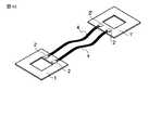
(第1の実施形態)
図1は、本発明の第1の実施形態に係わるLSIパッケージ接続用インターフェイスモジュールの概略構成を示す斜視図である。(First embodiment)
FIG. 1 is a perspective view showing a schematic configuration of an LSI package connection interface module according to the first embodiment of the present invention.
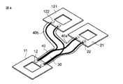
図中の11,21はLSIパッケージ(図示せず)と接続される平板状の接続体、12,22は光電変換部、30は補強フィルム、40はリボン光ファイバ(光伝送路)である。第1の接続体11の一辺側に偏って光電変換部12が設けられ、第2の接続体21の一辺側に偏って光電変換部22が設けられ、第1の接続体11と第2の接続体21は光電変換部12,22を設けた側の辺を対向させて離間配置されている。 In the figure,
接続体11,21は、例えばガラスエポキシ基板(UL規格のFR−4など)に所定の電気配線を設けたものであり、その中央にLSIパッケージのLSIが挿入される開口部が設けられている。光電変換部12,22は、例えばVCSEL(Vertical Cavity Surface Emitting Laser diode)やPIN−PD(P-I-N Photo-Diode)等の面入出力型の光素子と光ファイバを直接対向接続(バットジョイント)させ、光素子を駆動用のICに接続したものである。接続体11,12の電気配線(図示せず)はLSIパッケージに設けられた電極と光電変換部12,22を接続する。なお、光電変換部12,22は上記のような面入出力型光素子を複数個設けたものでも良いし、入力型光素子と出力型光素子とを別々に設けたものであっても良い。 The
リボン光ファイバ40は、例えばコア径50μm、クラッド径125μmのGI(Graded Index)型マルチモード光ファイバ素線を、250μmピッチで1次元アレイ化したものである。補強フィルム30としては、例えば2枚のポリイミドフィルム(例えば、厚さ100μm)を用い、これらのポリイミドフィルムでリボン光ファイバ40を上下から挟み込んで、接続体11,21にその端部を固定したものとする。 The ribbon
補強フィルム30とリボン光ファイバ40の構成例は、例えば図2のようにする。図2において、41は光ファイバ素線であり、詳細は図示していないが光導波部であるコアと光閉じ込めのためのクラッドからなる同軸構造になっている。また、42は光ファイバ素線41を束ねるための樹脂被覆であり、図2のような単純被覆のほか、各光ファイバ素線を被覆する個別の被覆と、それを更に束ねる全体被覆の二重構造としても構わない。 A configuration example of the reinforcing
図2の30a,30bは前述した補強フィルム30であり、例えばそれぞれ100μm厚のポリイミドフィルムとする。また、50(50a,50b)は補強フィルム貼り付けのための粘着剤であり、例えばシリコーン系又はアクリル系で厚さ50μmの粘着フィルムを用いる。補強フィルム30と粘着剤50は独立なシートとしても良いし、予め30aと50a、30bと50bがそれぞれ貼り付けられた粘着シートとしても構わない。補強フィルム30の端部は、接続体11,21に貼り付けても、接続体内に埋め込んでも良く、接続体11,21に例えば25N以上の引っ張り強度を持つように把持させる。
図3は、接続体11の構造を示す断面図であり、(a)は接続体11の一主面に補強フィルム30を貼り付けた例、(b)は接続体11に補強フィルム30を挟み込んだ例を示している。 3A and 3B are cross-sectional views illustrating the structure of the
図3(a)のように、接続体11の一主面に補強フィルム30を貼り付ける場合、接続体11の光電変換部12を搭載した面に配線13を形成し、配線13の一部にLSIパッケージの電極と接続するための電極パッド14を設けるようにすればよい。また、図3(b)のように、2枚の構成材11a,11bからなる接続体11に補強フィルム30を挟み込む場合、接続体11の内部に配線13を設け、接続体11の下面側にビアプラグ等を介して配線13を引き出し、この引き出し部分にLSIパッケージの電極と接続するための電極パッド14を設けるようにすればよい。As shown in FIG. 3A, when the reinforcing
このように本実施形態によれば、LSIパッケージとインターフェイスモジュールを分離可能とし、インターフェイスモジュールに光伝送路としてのリボン光ファイバ40を直付けしたLSI間光配線において、光配線路を補強するための補強フィルム30を設け、その補強フィルム30をインターフェイスモジュール本体に把持させることでインターフェイスモジュールとリボン光ファイバ40との境界部でのファイバ破損(鋭角曲げによる破断など)を防止することができる。 As described above, according to the present embodiment, the LSI package and the interface module can be separated, and the optical wiring path is reinforced in the inter-LSI optical wiring in which the ribbon
上記の破損防止効果に関する本発明者らの実験結果の一例を、以下に示す。 An example of the results of experiments by the inventors regarding the above-described damage prevention effect is shown below.
コア径50μm、クラッド径125μmのGI(Graded Index)型マルチモード光ファイバ素線を、250μmピッチで12本1次元アレイ化したリボン光ファイバ(被覆樹脂を含むリボンの厚さ270μm)において、角部の曲率半径0.1mmのアルミブロックによりリボン光ファイバを直角方向に曲げる引っ張り破断試験を行った。従来のように、何もカバーしてないリボン光ファイバの破断引張り力が約20Nであったのに対し、本実施形態のように、粘着剤を含むテープ厚さが70μmのポリイミドテープによりラミネートしたリボン光ファイバの破断引張り力は50N以上に強化された。 In a ribbon optical fiber (thickness of a ribbon including a coating resin: 270 μm) in which a GI (Graded Index) type multimode optical fiber having a core diameter of 50 μm and a cladding diameter of 125 μm is arranged in a one-dimensional array at a pitch of 250 μm, A tensile fracture test was conducted in which the ribbon optical fiber was bent in a right angle direction with an aluminum block having a curvature radius of 0.1 mm. The ribbon optical fiber that does not cover anything has a breaking tensile force of about 20 N as in the prior art, but is laminated with a polyimide tape having a thickness of 70 μm including an adhesive as in this embodiment. The breaking tensile force of the ribbon optical fiber was strengthened to 50 N or more.
また、同じリボン光ファイバを平行平板に挟んで折り返し、リボン光ファイバが破断する平行平板のギャップを測定したところ、補強フィルムの有無に拘わらず破断ギャップは2.5mm前後であった。そこで、破断ギャップより曲率がきつくなる直径1.6mmの丸棒でリボンファイバを折り返して引っ張り、180度折り返し曲げでリボン光ファイバが破断する引っ張り力を調べてみたところ、何もカバーしてないリボン光ファイバの破断引張り力が約5Nであったのに対し、粘着剤を含むテープ厚さが70μmのポリイミドテープによりラミネートしたリボン光ファイバの破断引張り力は約18Nと3倍以上の強度に向上することが分かった。 Further, when the same ribbon optical fiber was folded between parallel flat plates and the gap of the parallel flat plate where the ribbon optical fiber was broken was measured, the break gap was about 2.5 mm regardless of the presence or absence of the reinforcing film. Therefore, when the ribbon fiber was folded and pulled with a round bar with a diameter of 1.6 mm whose curvature was tighter than the breaking gap, and the tensile force at which the ribbon optical fiber was broken by folding back 180 degrees was examined, a ribbon that did not cover anything The breaking tensile force of the optical fiber was about 5 N, whereas the breaking tensile force of the ribbon optical fiber laminated with a polyimide tape having a thickness of 70 μm including the adhesive was about 18 N, which is three times higher than the strength. I understood that.
このように、リボン光ファイバ40に補強フィルム30を設けることで曲げの破断強度を向上可能であり、リボン光ファイバ40の取り付け部での破断を起き難くすることができる。また、補強フィルム30は、リボン光ファイバ40の片側に設けることでも効果を持つが、リボンファイバ40を上下いずれの方向にも破断し難くするため、リボンファイバ40の両側に設けることが望ましい。 As described above, by providing the reinforcing
以上のインターフェイスモジュールは、まず対向する2つの光電変換部12,22にリボン光ファイバ40を取り付け、その後、2つの接続体11,21にそれぞれの光電変換部12,22を搭載、さらに補強フィルム30を貼り付けるといった工程で作製可能である。また、プリント基板の製造工程を利用し、光ファイバ等による光配線部を予め切り抜いた形の多数個取り基板を積層張り合わせしていく製法を用いることもできる。例えば、下側基板(接続体11、21となるもの)、下側補強フィルム、光電変換部及び光配線路組立て品、上側補強フィルム、上側基板(接続体11、21となるもの)というように積層していくことで、一括して多数個のインターフェイスモジュールを連続的に生産することも可能である。 In the above interface module, the ribbon
これは、所謂リジッドフレックス基板の製造方法を取り入れることが可能ということを意味している。即ち、光配線の高速大容量配線特性はそのままに、光配線のコストと量産性を大幅に高めることが可能となり、これにより情報通信機器等の高度化に大きく貢献することができる。 This means that a so-called rigid flex substrate manufacturing method can be adopted. That is, it is possible to greatly increase the cost and mass productivity of the optical wiring while maintaining the high-speed and large-capacity wiring characteristics of the optical wiring, which can greatly contribute to the advancement of information communication equipment and the like.
(第2の実施形態)
図4は、本発明の第2の実施形態に係わるLSIパッケージ接続用インターフェイスモジュールの概略構成を示す斜視図である。なお、図1と同一部分には同一符号を付して、その詳しい説明は省略する。(Second Embodiment)
FIG. 4 is a perspective view showing a schematic configuration of an LSI package connection interface module according to the second embodiment of the present invention. In addition, the same code | symbol is attached | subjected to FIG. 1 and an identical part, and the detailed description is abbreviate | omitted.
本実施形態は、リボン光ファイバ40を途中で分岐し、分岐したそれぞれに接続体を設けるようにしたものである。即ち、接続体11からのリボン光ファイバ40は途中で40a,40bの2つに分岐され、各々の分岐ファイバ40a,40bに異なる接続体が接続されている。 In the present embodiment, the ribbon
具体的には、分岐ファイバ40aは第2の接続体21の光電変換部22に接続され、分岐ファイバ40bは第3の接続体121の光電変換部122に接続されている。分岐ファイバ40a,40bもリボン光ファイバ40と同様に、補強フィルム30により挟み込まれている。 Specifically, the
このような構成であっても、先の第1の実施形態と同様の効果が得られる。これに加えて本実施形態では、2つに限らず3つのLSIパッケージを接続することができる。また、ファイバ40の分岐数を増やすことにより、更に多くのLSIパッケージを接続することも可能である。 Even if it is such a structure, the effect similar to previous 1st Embodiment is acquired. In addition to this, in the present embodiment, not only two but also three LSI packages can be connected. Further, by increasing the number of branches of the
(第3の実施形態)
図5は、本発明の第3の実施形態に係わるLSIパッケージ接続用インターフェイスモジュールの概略構成を示す斜視図である。なお、図1と同一部分には同一符号を付して、その詳しい説明は省略する。(Third embodiment)
FIG. 5 is a perspective view showing a schematic configuration of an LSI package connection interface module according to the third embodiment of the present invention. In addition, the same code | symbol is attached | subjected to FIG. 1 and an identical part, and the detailed description is abbreviate | omitted.
本実施形態は、接続体11において、1つの辺に沿ってのみに光電変換部12を設けるのではなく、矩形状の接続体11の4つの辺のそれぞれに沿って光電変換部12を設けるようにしたものである。そして、接続体11には、4つの辺に対し直交する方向からそれぞれ補強フィルム30及びリボンファイバ40が接続されている。 In the present embodiment, in the
本実施形態のLSIパッケージ接続用インターフェイスモジュールを用いることによって、1つのLSIパッケージに対して複数のLSIパッケージを接続することが可能となる。 By using the LSI package connection interface module of the present embodiment, a plurality of LSI packages can be connected to one LSI package.
(第4の実施形態)
図6は、本発明の第4の実施形態に係わるLSIパッケージ用インターフェイスモジュールの概略構成を示す斜視図である。なお、図1と同一部分には同一符号を付して、その詳しい説明は省略する。(Fourth embodiment)
FIG. 6 is a perspective view showing a schematic configuration of an LSI package interface module according to the fourth embodiment of the present invention. In addition, the same code | symbol is attached | subjected to FIG. 1 and an identical part, and the detailed description is abbreviate | omitted.
本実施形態は、2つの接続体11,21間を光伝送路で接続するのではなく、1つの接続体11に対して光伝送路を接続したものである。即ち、第1の実施形態と同様に、接続体11には光電変換部12が設けられている。この光電変換部12に光学的に接続するようにリボンファイバ40が接続され、更にリボンファイバ40を覆うように補強フィルム30が設けられている。ここで、リボンファイバ30の他方の端部は、図6(a)に示すように単に開放としても良いし、図6(b)に示すように光コネクタ15に接続するようにしても良い。 In the present embodiment, the two
本実施形態のLSIパッケージ用インターフェイスモジュールを用いることにより、2つのLSIパッケージの接続に限らず、1つのLSIパッケージに対して各種のデバイスを接続することが可能となる。また、図6(a)(b)のペアを用いることにより、第1の実施形態と同様に、2つのLSIパッケージの接続も可能である。 By using the LSI package interface module of this embodiment, it is possible to connect various devices to one LSI package as well as two LSI packages. Further, by using the pair of FIGS. 6A and 6B, it is possible to connect two LSI packages as in the first embodiment.
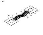
(第5の実施形態)
図7は、本発明の第5の実施形態に係わるLSIパッケージ接続用インターフェイスモジュールの概略構成を示す斜視図である。なお、図1と同一部分には同一符号を付して、その詳しい説明は省略する。(Fifth embodiment)
FIG. 7 is a perspective view showing a schematic configuration of an LSI package connection interface module according to the fifth embodiment of the present invention. In addition, the same code | symbol is attached | subjected to FIG. 1 and an identical part, and the detailed description is abbreviate | omitted.
本実施形態は、第1の実施形態の構成に加え、2つの接続体11,21間を電気的に接続するための配線を設けたものである。即ち、リボンファイバ40と並んで電気配線路としての配線60が配置され、配線60はリボンファイバ40と共に補強フィルム30に上下から挟み込まれている。配線60は、例えば50μm厚のポリイミドフィルムコアに200μm幅で18μm厚の銅メッキ配線を設けたものである。 In the present embodiment, in addition to the configuration of the first embodiment, wiring for electrically connecting the two connecting
配線60の一端は接続体11に設けた配線に接続され、他端は接続体21に設けた配線に接続されている。補強フィルム30は、例えば2枚のポリイミドフィルム(例えば、厚さ100μm)でリボン光ファイバ40及び配線60を上下からラミネートし、一端が接続体11に固定され、他端が接続体21に固定されている。 One end of the
補強フィルム30とリボン光ファイバ40及び配線60の構成例は、例えば図8のようにする。図8において、41は光ファイバ素線であり、詳細は図示していないが光導波部であるコアと光閉じ込めのためのクラッドからなる同軸構造になっている。また、42は光ファイバ素線41を束ねるための樹脂被覆であり、図8のような単純被覆のほか、各光ファイバ素線を被覆する個別の被覆と、それを更に束ねる全体被覆の二重構造としても構わない。 A configuration example of the reinforcing
図8の30a,30bは前述した補強フィルム30であり、例えばそれぞれ100μm厚のポリイミドフィルムとする。また、50(50a,50b)は補強フィルム貼り付けのための粘着剤であり、例えばシリコーン系又はアクリル系で厚さ50μmのものを用いる。補強フィルム30と粘着剤50は独立なシートとしても、予め30aと50a、30bと50bがそれぞれ貼り付けられた粘着シートとしても構わない。
図8の30cは電気配線基材(コア)であり、例えば50μm厚のポリイミドフィルムを用いる。電気配線基材30cの両面には配線60(60a,60b)が設けられ、LSIパッケージ間の専用電気配線とする。配線60a,60bは、例えば18μm厚で200μm幅の銅パターンとする。補強フィルム30の端部は、接続体11,21に貼り付けても、接続体内に埋め込んでも良く、接続体11,21に例えば25N以上の引っ張り強度を持つように把持させる。
このように構成することにより、インターフェイスモジュールと光配線路の境界部での光配線路破損(鋭角曲げによる破断など)を防止することが可能なほか、LSIパッケージ間の専用電気配線が確保でき、制御信号などの低速信号を他の部品からのノイズを受け難い状態で配線することが可能になる。 By configuring in this way, it is possible to prevent optical wiring path breakage (breakage due to acute angle bending, etc.) at the interface module and optical wiring path boundary, as well as secure dedicated electrical wiring between LSI packages, A low-speed signal such as a control signal can be wired in a state where it is difficult to receive noise from other components.
以上のインターフェイスモジュールは、まず対向する2つの光電変換部12,22にリボン光ファイバ40を取り付け、その後、2つの接続体11,21にそれぞれの光電変換部12,22を搭載、更に配線60を搭載、最後に補強フィルム30を貼り付けるといった工程で作製可能である。しかしながら、プリント基板の製造工程を利用し、光ファイバ等による光配線部を予め切り抜いた形の多数個取り基板を積層張り合わせしていく製法を用いる。例えば、下側基板(接続体11、21となるもの)、下側補強フィルム、光電変換部付き光配線路及び電気配線基材、上側補強フィルム、上側基板(接続体11、21となるもの)というように積層していくことで、一括して多数個のインターフェイスモジュールを連続的に生産することも可能である。これは、即ち、所謂リジッドフレックス基板の製造方法を取り入れることが可能ということを示している。 In the above interface module, the ribbon
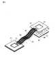
(第6の実施形態)
図9は、本発明の第6の実施形態に係わるLSI実装体の概略構成を示す斜視図である。なお、図7と同一部分には同一符号を付して、その詳しい説明は省略する。(Sixth embodiment)
FIG. 9 is a perspective view showing a schematic configuration of an LSI package according to the sixth embodiment of the present invention. The same parts as those in FIG. 7 are denoted by the same reference numerals, and detailed description thereof is omitted.
本実施形態は、図7で示したインターフェイスモジュールをプリント基板(図示せず)上のLSIパッケージに装着する状況を示している。図9において、70はLSIチップ、80はLSIパッケージである。LSIパッケージ80は、下側にプリント基板接続用電極(半田ボール)81、上側のLSIチップ搭載部以外の部分でインターフェイスモジュール接続用電極(電極パッド)82を有するものとする。 This embodiment shows a situation where the interface module shown in FIG. 7 is mounted on an LSI package on a printed circuit board (not shown). In FIG. 9,
図9では、LSIパッケージとしてBGA(Ball Grid Array)を示しているが、これはPGA(Pin Grid Array)、LGA(Land Grid Array)等としても適用可能なものである。 In FIG. 9, a BGA (Ball Grid Array) is shown as an LSI package, but this can also be applied to a PGA (Pin Grid Array), an LGA (Land Grid Array), or the like.
インターフェイスモジュールは、プリント基板(図示せず)上に他の部品と共にLSIパッケージ80を実装した後、図9に示すように、上側から被せるように搭載する。その際、インターフェイスモジュールの接続体11,21のLSIチップ70が位置する部分をくり抜いておくと、図9に示すようにLSIチップ70の上面(フリップチップ実装の場合はLSIチップ基板面)が露出し、ここからLSIチップ70の放熱を行うことができる。即ち、図9左側のLSIパッケージの状態でヒートシンクを乗せることで、LSIチップ70の放熱を確保できる。 After mounting the
なお、図9においては、2つのLSIパッケージを光配線する例で示しているが、3つ以上のLSIパッケージを光配線する場合にも本発明が適用できる。3つ以上のLSIパッケージを光配線する場合、まず、接続体はLSIパッケージの数だけ用意する。そして、各LSIパッケージの配線アーキテクチャに応じ、各接続体に用意する光電変換部の間を接続する光伝送路の配線パターンを決定する。 Although FIG. 9 shows an example in which two LSI packages are optically wired, the present invention can also be applied to a case where three or more LSI packages are optically wired. In the case where three or more LSI packages are optically wired, first, as many connection bodies as the number of LSI packages are prepared. Then, according to the wiring architecture of each LSI package, the wiring pattern of the optical transmission line that connects between the photoelectric conversion units prepared in each connection body is determined.
このとき、光伝送路40は図9のようにアレイのまま直線的に配置するだけでなく、先の第2の実施形態のように、光伝送路40を分岐させたり、先の第3の実施形態のように、光伝送路40を個別に分離して引き回すパターンとしても構わない。また、同時に電気配線路も配線パターンを決定するが、光伝送路との交差部があっても配線可能なため、光伝送路と電気配線路は別々に設計されても問題ない。最後に、各光伝送路40と電気配線路60を補強フィルム30で覆い、その端部を各接続体の光配線及び電気配線引き出し部領域で把持するようにする。 At this time, the
このようにすることで、3つ以上のLSIパッケージも1つのインターフェイスモジュールで高速配線することができ、システム構成や実装構成のフレキシビリティーを格段に広げることが可能になる
(変形例)
なお、本発明は上述した各実施形態に限定されるものではない。実施形態では各具体構成を示しているが、これはあくまで構成例であり、本発明の主旨に従い個々の要素に他の具体手段(部品、材料)を用いても構わないものである。また、実施形態に示された材料、形状、配置などはあくまで一例であり、また、各実施形態を組み合わせて実施することも可能である。In this way, three or more LSI packages can be wired at high speed with one interface module, and the flexibility of the system configuration and mounting configuration can be greatly expanded.
The present invention is not limited to the above-described embodiments. Although each specific configuration is shown in the embodiment, this is merely an exemplary configuration, and other specific means (parts, materials) may be used for individual elements in accordance with the gist of the present invention. In addition, the materials, shapes, arrangements, and the like shown in the embodiments are merely examples, and the embodiments can be implemented in combination.
要するに本発明は、その要旨を逸脱しない範囲で、種々変形して実施することができるものである。 In short, the present invention can be implemented with various modifications without departing from the spirit of the present invention.
11,21,121…接続体
12,22,122…光電変換部
13…配線
14…電極パッド
15…光コネクタ
30…補強フィルム
40…リボン光ファイバ(光伝送路)
41…光ファイバ素線
42…樹脂被覆
50…粘着剤
60…配線(電気配線路)
70…LSIチップ
80…LSIパッケージ
81…プリント基板接続用電極
82…インターフェイスモジュール接続用電極11, 21, 121 ...
DESCRIPTION OF
70 ...
Claims (14)
Translated fromJapanese前記接続体の一主面上に搭載され、前記配線に電気的に接続され、光−電気変換若しくは電気−光変換を行う光電変換部と、
一方の光入出力端が前記光電変換部に光学的に接続された光伝送路と、
前記光伝送路の少なくとも一側面を覆って該光伝送路に接着されると共に、一端側が前記接続体の一主面に固定された補強フィルムと、
を具備したことを特徴とするLSIパッケージ用インターフェイスモジュール。A plate-like connection body mounted on an LSI package on which an LSI chip is mounted and having a wiring electrically connected to an electrode of the package;
A photoelectric conversion unit that is mountedon one main surface of the connection bodyand is electrically connected to the wiring and performs optical-electrical conversion or electrical-optical conversion;
An optical transmission line in which one light input / output end is optically connected to the photoelectric conversion unit;
A reinforcing film that covers at least one side surface of the optical transmission path and is bonded to the optical transmission path, and one endside of which is fixed toone main surface of the connection body;
An interface module for an LSI package, comprising:
第2のLSIパッケージに装着され、該パッケージの電極と電気的に接続される配線を有する第2の接続体と、
前記第1及び第2の接続体の一主面上にそれぞれ搭載され、それぞれの前記配線に電気的に接続され、光−電気変換若しくは電気−光変換を行う光電変換部と、
一方の光入出力端が前記第1の接続体に搭載された光電変換部に光学的に接続され、他方の光入出力端が前記第2の接続体に搭載された光電変換部に光学的に接続された光伝送路と、
前記光伝送路の少なくとも一側面を覆って該光伝送路に接着されると共に、一端側が前記第1の接続体の一主面に固定され、他端側が前記第2の接続体の一主面に固定された補強フィルムと、
を具備したことを特徴とするLSIパッケージ用インターフェイスモジュール。A plate-like first connection body mounted on the first LSI package and having a wiring electrically connected to an electrode of the package;
A second connection body mounted on the second LSI package and having a wiring electrically connected to an electrode of the package;
A photoelectric conversion unit mountedon one main surface of each of the first and second connection bodies, electrically connected to each of the wirings, and performing optical-electrical conversion or electrical-optical conversion;
One optical input / output end is optically connected to the photoelectric conversion unit mounted on the first connection body, and the other optical input / output end is optically connected to the photoelectric conversion unit mounted on the second connection body. An optical transmission line connected to
At least one side surface of the optical transmission line is covered and adhered to the optical transmission line, one endside is fixed toone main surface ofthe first connection body, and the other endside is oneside of the second connection body. A reinforcing film fixed to themain surface ;
An interface module for an LSI package, comprising:
LSIチップを搭載し、前記実装基板上にそれぞれ搭載された第1及び第2のLSIパッケージと、
前記第1及び第2のLSIパッケージにそれぞれ装着され、該LSIパッケージ間を光学的に接続するLSIパッケージ用インターフェイスモジュールと、
を具備し、
前記LSIパッケージ用インターフェイスモジュールは、
第1のLSIパッケージの電極に装着され、該パッケージと電気的に接続される配線を有する第1の接続体と、
第2のLSIパッケージの電極に装着され、該パッケージと電気的に接続される配線を有する第2の接続体と、
前記第1及び第2の接続体の一主面上にそれぞれ搭載され、前記配線に電気的に接続され、光−電気変換若しくは電気−光変換を行う光電変換部と、
一方の光入出力端が前記第1の接続体に搭載された光電変換部に光学的に接続され、他方の光入出力端が前記第2の接続体に搭載された光電変換部に光学的に接続された光伝送路と、
前記光伝送路の少なくとも一側面を覆って該光伝送路に接着されると共に、一端側が前記第1の接続体の一主面に固定され、他端側が前記第2の接続体の一主面に固定された補強フィルムと、
を有することを特徴とするLSI実装体。A mounting board;
An LSI chip, and first and second LSI packages respectively mounted on the mounting substrate;
An LSI package interface module mounted on each of the first and second LSI packages and optically connecting the LSI packages;
Comprising
The LSI package interface module includes:
A first connection body mounted on an electrode of the first LSI package and having a wiring electrically connected to the package;
A second connection body mounted on an electrode of the second LSI package and having a wiring electrically connected to the package;
A photoelectric conversion unit mountedon one main surface of each of the first and second connection bodies, electrically connected to the wiring, and performing photoelectric conversion or photoelectric conversion;
One optical input / output end is optically connected to the photoelectric conversion unit mounted on the first connection body, and the other optical input / output end is optically connected to the photoelectric conversion unit mounted on the second connection body. An optical transmission line connected to
At least one side surface of the optical transmission line is coveredand adhered to the optical transmission line, one endside is fixed toone main surface ofthe first connection body, and the other endside is oneside of the second connection body. A reinforcing film fixed to themain surface ;
An LSI mounting body characterized by comprising:
Priority Applications (2)
| Application Number | Priority Date | Filing Date | Title |
|---|---|---|---|
| JP2005052709AJP4468210B2 (en) | 2005-02-28 | 2005-02-28 | LSI package interface module and LSI package |
| US11/233,175US7312520B2 (en) | 2005-02-28 | 2005-09-23 | Interface module for connecting LSI packages, and LSI-incorporating apparatus |
Applications Claiming Priority (1)
| Application Number | Priority Date | Filing Date | Title |
|---|---|---|---|
| JP2005052709AJP4468210B2 (en) | 2005-02-28 | 2005-02-28 | LSI package interface module and LSI package |
Publications (2)
| Publication Number | Publication Date |
|---|---|
| JP2006237449A JP2006237449A (en) | 2006-09-07 |
| JP4468210B2true JP4468210B2 (en) | 2010-05-26 |
Family
ID=36931310
Family Applications (1)
| Application Number | Title | Priority Date | Filing Date |
|---|---|---|---|
| JP2005052709AExpired - LifetimeJP4468210B2 (en) | 2005-02-28 | 2005-02-28 | LSI package interface module and LSI package |
Country Status (2)
| Country | Link |
|---|---|
| US (1) | US7312520B2 (en) |
| JP (1) | JP4468210B2 (en) |
Families Citing this family (25)
| Publication number | Priority date | Publication date | Assignee | Title |
|---|---|---|---|---|
| US7352935B2 (en) | 2004-08-17 | 2008-04-01 | Kabushiki Kaisha Toshiba | Optoelectronic conversion header, LSI package with interface module, method of manufacturing optoelectronic conversion header, and optical interconnection system |
| JP4468210B2 (en) | 2005-02-28 | 2010-05-26 | 株式会社東芝 | LSI package interface module and LSI package |
| JP4934325B2 (en)* | 2006-02-17 | 2012-05-16 | 株式会社フジクラ | Printed wiring board connection structure and printed wiring board connection method |
| US8107776B2 (en)* | 2006-09-19 | 2012-01-31 | Ibiden Co., Ltd. | Optical interconnect device and method for manufacturing the same |
| KR100825732B1 (en)* | 2006-09-29 | 2008-04-29 | 한국전자통신연구원 | Photoelectric connector module and photoelectric communication module including the module |
| US7547908B2 (en)* | 2006-12-22 | 2009-06-16 | Philips Lumilieds Lighting Co, Llc | III-nitride light emitting devices grown on templates to reduce strain |
| JP2008292660A (en)* | 2007-05-23 | 2008-12-04 | Fujikura Ltd | Optical fiber, optical communication module |
| JP4825739B2 (en)* | 2007-06-22 | 2011-11-30 | 株式会社日立製作所 | Structure of opto-electric hybrid board and opto-electric package |
| US7747116B2 (en)* | 2007-09-05 | 2010-06-29 | Kabushiki Kaisha Toshiba | Flexible optoelectric interconnect and method for manufacturing same |
| JP2009103878A (en)* | 2007-10-23 | 2009-05-14 | Fuji Xerox Co Ltd | Optical reception and transmission module |
| JP4613964B2 (en)* | 2008-01-21 | 2011-01-19 | 富士ゼロックス株式会社 | Photoelectric composite wiring module and information processing apparatus |
| JP5066134B2 (en)* | 2009-05-28 | 2012-11-07 | 株式会社東芝 | Optical wiring cable |
| JP2010286777A (en)* | 2009-06-15 | 2010-12-24 | Toshiba Corp | Photoelectric wiring film and photoelectric wiring module |
| JP2011017985A (en)* | 2009-07-10 | 2011-01-27 | Molex Inc | Optical connector assembly, cable for use with optical connector assembly, and plug for use with optical connector assembly |
| JP5290074B2 (en) | 2009-07-13 | 2013-09-18 | モレックス インコーポレイテド | Optical connector |
| JP2011022198A (en) | 2009-07-13 | 2011-02-03 | Molex Inc | Optical connector |
| JP2011053354A (en)* | 2009-08-31 | 2011-03-17 | Toshiba Corp | Optoelectronic wiring film and optoelectronic wiring module |
| JP2011066086A (en)* | 2009-09-15 | 2011-03-31 | Toshiba Corp | Flexible wiring board array, method of manufacturing the same, and flexible wiring device |
| JP2013167750A (en)* | 2012-02-15 | 2013-08-29 | Hitachi Cable Ltd | Photoelectric composite wiring module |
| US20140312450A1 (en)* | 2013-04-23 | 2014-10-23 | Sensors Unlimited, Inc. | Small Size, Weight, and Packaging of Image Sensors |
| US10026882B2 (en)* | 2014-10-07 | 2018-07-17 | Epistar Corporation | Using MEMS fabrication incorporating into LED device mounting and assembly |
| JP6423930B1 (en)* | 2017-07-28 | 2018-11-14 | Smk株式会社 | Photoelectric composite cable |
| JP7610911B2 (en)* | 2020-01-30 | 2025-01-09 | 株式会社キーエンス | Optical detection unit |
| CN114114528B (en) | 2020-08-28 | 2023-06-02 | 深南电路股份有限公司 | Optical fiber circuit board assembly and photoelectric hybrid circuit board |
| CN115175435B (en)* | 2021-04-07 | 2025-06-13 | 深南电路股份有限公司 | Optical fiber circuit board components and optoelectronic hybrid circuit boards |
Family Cites Families (12)
| Publication number | Priority date | Publication date | Assignee | Title |
|---|---|---|---|---|
| US5535296A (en)* | 1994-09-28 | 1996-07-09 | Optobahn Corporation | Integrated optoelectronic coupling and connector |
| JPH0980279A (en)* | 1995-09-08 | 1997-03-28 | Sumitomo Electric Ind Ltd | Tape type optical fiber cable |
| JP3705873B2 (en)* | 1996-10-17 | 2005-10-12 | 株式会社アドバンテスト | Optical / electric mixed wiring board |
| JP2002169037A (en)* | 2000-12-01 | 2002-06-14 | Sumitomo Electric Ind Ltd | Optical wiring components and electrical boards |
| JP3784699B2 (en)* | 2001-11-16 | 2006-06-14 | 株式会社フジクラ | Optical fiber array |
| KR20050007459A (en)* | 2002-04-16 | 2005-01-18 | 엑스룸 포토닉스 리미티드 | Electro-optical circuitry having integrated connector and methods for the production thereof |
| US6864553B2 (en)* | 2002-07-30 | 2005-03-08 | Intel Corporation | Method and apparatus for a backsided and recessed optical package connection |
| JP4131935B2 (en)* | 2003-02-18 | 2008-08-13 | 株式会社東芝 | Interface module, LSI package with interface module, and mounting method thereof |
| DE10332015A1 (en)* | 2003-07-14 | 2005-03-03 | Infineon Technologies Ag | Optoelectronic module with transmitter chip and connector for the module to an optical fiber and to a circuit board, and method of making the same |
| DE10342263A1 (en)* | 2003-09-11 | 2005-04-28 | Infineon Technologies Ag | Optoelectronic component and optoelectronic arrangement with an optoelectronic component |
| JP3917133B2 (en) | 2003-12-26 | 2007-05-23 | 株式会社東芝 | LSI package with interface module and interposer, interface module, connection monitor circuit, signal processing LSI used therefor |
| JP4468210B2 (en) | 2005-02-28 | 2010-05-26 | 株式会社東芝 | LSI package interface module and LSI package |
- 2005
- 2005-02-28JPJP2005052709Apatent/JP4468210B2/ennot_activeExpired - Lifetime
- 2005-09-23USUS11/233,175patent/US7312520B2/ennot_activeExpired - Fee Related
Also Published As
| Publication number | Publication date |
|---|---|
| US20060192278A1 (en) | 2006-08-31 |
| JP2006237449A (en) | 2006-09-07 |
| US7312520B2 (en) | 2007-12-25 |
Similar Documents
| Publication | Publication Date | Title |
|---|---|---|
| JP4468210B2 (en) | LSI package interface module and LSI package | |
| KR100911508B1 (en) | Photoelectric integrated circuit device and transmission device using same | |
| US8363993B2 (en) | Combined optical and electrical interconnection module and method for producing same | |
| JP4876263B2 (en) | Signal transmission equipment | |
| JP5439080B2 (en) | Optical I/O Array Module | |
| US7275937B2 (en) | Optoelectronic module with components mounted on a flexible circuit | |
| US7306377B2 (en) | Integrated optical sub-assembly having epoxy chip package | |
| US8285087B2 (en) | Optical interconnection system using optical printed circuit board having one-unit optical waveguide integrated therein | |
| US20100316335A1 (en) | Optoelectronic interconnection film, and optoelectronic interconnection module | |
| JP2009003253A (en) | Structure of opto-electric hybrid board and opto-electric package | |
| JP2008015336A (en) | Circuit board and semiconductor device optical coupling method | |
| JP2006091241A (en) | Opto-electric composite wiring component and electronic device using the same | |
| US20110188816A1 (en) | Flexible optoelectronic interconnection module and method of manufacturing the same | |
| US20120224804A1 (en) | Semiconductor device and method of manufacturing the same | |
| US8867231B2 (en) | Electronic module packages and assemblies for electrical systems | |
| JP5692581B2 (en) | Photoelectric conversion module and method for manufacturing photoelectric conversion module | |
| JP5093121B2 (en) | Optical module | |
| JP2012195456A (en) | Flexible wiring module and flexible wiring device | |
| JP2014122929A (en) | Optical waveguide device and manufacturing method therefor | |
| EP2211217A1 (en) | Printed circuit board fiberoptical transceiver in surface mount technology (SMT) | |
| JP2013097147A (en) | Flexible optoelectronic interconnection module | |
| JP2011043535A (en) | Optical connection device and method of manufacturing the same | |
| CN115175435B (en) | Optical fiber circuit board components and optoelectronic hybrid circuit boards | |
| CN223180456U (en) | Electronic devices | |
| JP2011227371A (en) | Semiconductor package |
Legal Events
| Date | Code | Title | Description |
|---|---|---|---|
| A131 | Notification of reasons for refusal | Free format text:JAPANESE INTERMEDIATE CODE: A131 Effective date:20090113 | |
| A521 | Request for written amendment filed | Free format text:JAPANESE INTERMEDIATE CODE: A523 Effective date:20090309 | |
| TRDD | Decision of grant or rejection written | ||
| A01 | Written decision to grant a patent or to grant a registration (utility model) | Free format text:JAPANESE INTERMEDIATE CODE: A01 Effective date:20100126 | |
| A01 | Written decision to grant a patent or to grant a registration (utility model) | Free format text:JAPANESE INTERMEDIATE CODE: A01 | |
| A61 | First payment of annual fees (during grant procedure) | Free format text:JAPANESE INTERMEDIATE CODE: A61 Effective date:20100224 | |
| FPAY | Renewal fee payment (event date is renewal date of database) | Free format text:PAYMENT UNTIL: 20130305 Year of fee payment:3 |