JP4465995B2 - Probe sheet, probe card, semiconductor inspection apparatus, and semiconductor device manufacturing method - Google Patents
Probe sheet, probe card, semiconductor inspection apparatus, and semiconductor device manufacturing methodDownload PDFInfo
- Publication number
- JP4465995B2 JP4465995B2JP2003189949AJP2003189949AJP4465995B2JP 4465995 B2JP4465995 B2JP 4465995B2JP 2003189949 AJP2003189949 AJP 2003189949AJP 2003189949 AJP2003189949 AJP 2003189949AJP 4465995 B2JP4465995 B2JP 4465995B2
- Authority
- JP
- Japan
- Prior art keywords
- metal film
- electrodes
- contact
- probe sheet
- probe
- Prior art date
- Legal status (The legal status is an assumption and is not a legal conclusion. Google has not performed a legal analysis and makes no representation as to the accuracy of the status listed.)
- Expired - Lifetime
Links
Images


Classifications
- H—ELECTRICITY
- H01—ELECTRIC ELEMENTS
- H01L—SEMICONDUCTOR DEVICES NOT COVERED BY CLASS H10
- H01L22/00—Testing or measuring during manufacture or treatment; Reliability measurements, i.e. testing of parts without further processing to modify the parts as such; Structural arrangements therefor
- G—PHYSICS
- G01—MEASURING; TESTING
- G01R—MEASURING ELECTRIC VARIABLES; MEASURING MAGNETIC VARIABLES
- G01R1/00—Details of instruments or arrangements of the types included in groups G01R5/00 - G01R13/00 and G01R31/00
- G01R1/02—General constructional details
- G01R1/06—Measuring leads; Measuring probes
- G01R1/067—Measuring probes
- G01R1/06711—Probe needles; Cantilever beams; "Bump" contacts; Replaceable probe pins
- G01R1/06733—Geometry aspects
- G01R1/06744—Microprobes, i.e. having dimensions as IC details
- G—PHYSICS
- G01—MEASURING; TESTING
- G01R—MEASURING ELECTRIC VARIABLES; MEASURING MAGNETIC VARIABLES
- G01R1/00—Details of instruments or arrangements of the types included in groups G01R5/00 - G01R13/00 and G01R31/00
- G01R1/02—General constructional details
- G01R1/06—Measuring leads; Measuring probes
- G01R1/067—Measuring probes
- G01R1/073—Multiple probes
- G01R1/07307—Multiple probes with individual probe elements, e.g. needles, cantilever beams or bump contacts, fixed in relation to each other, e.g. bed of nails fixture or probe card
- G01R1/0735—Multiple probes with individual probe elements, e.g. needles, cantilever beams or bump contacts, fixed in relation to each other, e.g. bed of nails fixture or probe card arranged on a flexible frame or film
- G—PHYSICS
- G01—MEASURING; TESTING
- G01R—MEASURING ELECTRIC VARIABLES; MEASURING MAGNETIC VARIABLES
- G01R1/00—Details of instruments or arrangements of the types included in groups G01R5/00 - G01R13/00 and G01R31/00
- G01R1/02—General constructional details
- G01R1/06—Measuring leads; Measuring probes
- G01R1/067—Measuring probes
- G01R1/06711—Probe needles; Cantilever beams; "Bump" contacts; Replaceable probe pins
- G—PHYSICS
- G01—MEASURING; TESTING
- G01R—MEASURING ELECTRIC VARIABLES; MEASURING MAGNETIC VARIABLES
- G01R3/00—Apparatus or processes specially adapted for the manufacture or maintenance of measuring instruments, e.g. of probe tips
Landscapes
- Physics & Mathematics (AREA)
- General Physics & Mathematics (AREA)
- Geometry (AREA)
- Engineering & Computer Science (AREA)
- Manufacturing & Machinery (AREA)
- Computer Hardware Design (AREA)
- Microelectronics & Electronic Packaging (AREA)
- Power Engineering (AREA)
- Testing Or Measuring Of Semiconductors Or The Like (AREA)
- Measuring Leads Or Probes (AREA)
- Tests Of Electronic Circuits (AREA)
- Testing Of Individual Semiconductor Devices (AREA)
Description
Translated fromJapanese【0001】
【発明の属する技術分野】
本発明は、プローブシート、プローブカード、および半導体検査装置および半導体装置の製造方法に関する。
【0002】
【従来の技術】
半導体素子回路をウエハに形成後に行う半導体装置の製造工程のうち、主に検査工程の流れの一例を、代表的な半導体装置の出荷形態であるパッケージ品、ベアチップおよびCSPを例にして、図12に示した。
【0003】
半導体装置の製造工程では、図12に示したように大きく分けて次の3つの検査が行われる。まず、ウエハに半導体素子回路および電極を形成したウエハ状態で行われ、導通状態および半導体素子の電気信号動作状態を把握するウエハ検査、続いて半導体素子を高温や高印加電圧等の状態において不安定な半導体素子を摘出するバーンイン検査、そして半導体装置を出荷する前に製品性能を把握する選別検査である。
【0004】
このような半導体装置の検査に用いられる装置(半導体検査装置)の従来技術として、特許文献1がある(以下、従来技術1という)。この技術は、薄膜支持フレームと、この支持フレームに固定されたフレキシブルな薄膜と、試験される装置の接触パッド上に加圧されるように薄膜の外面の中央領域に設けられた複数の試験プローブ接触子と、各プローブ接触子を試験回路へ接続する薄膜上の複数の導電性トレースと、プローブ試験接触子が試験されるべき装置の接触パッド上に加圧されたときに前記薄膜中央領域を自動的に回動させる手段(中央領域の薄膜の内面に固定された加圧プレートとこの加圧プレートの中央をピボット的に加圧する頭部が半球形のピボットポストからなる)とを具備した自己水平化薄膜試験プローブが記載されている。
【0005】
他の従来技術として、特許文献2がある(以下、従来技術2という)。この技術は、支持部材と、先端を尖らせた接触端子をプロービング側の領域部に複数併設し、該各接触端子に電気的につながって引き出される複数の引き出し用配線と絶縁層を挟んでグランド層とを有する多層フィルムと、多層フィルムにおける裏側に固定された枠と、押さえ部材と、各接触端子の先端を各電極に接触させるための接触圧を前記支持部材から前記押さえ部材に対して付与する接触圧付与手段と、前記接触端子群の先端面を前記電極群の面に接触させる際、接触端子群の先端面が電極群の面に倣って平行出しするコンプライアンス機構とを備えた接続装置、及び該接続装置を検査対象物の電極に接触させることにより、電気的接続を取り検査を行う検査システムが記載されている。
【0006】
【特許文献1】
特開平7−7056号公報(特願平6-28200)
【特許文献2】
特開平11−23615号公報(特願平10-49912)
【0007】
【発明が解決しようとする課題】
しかし、上記従来技術1では、接触端子を接触端子を加圧するために薄膜の周辺部を固着し、薄膜全体が伸びて張った状態で、加圧する方式である。したがって加圧プレートと被検査対象物との平行出しは、薄膜の張力に依存しており、また、薄膜を配線基板下面から張り出させる場合、大きな引っ張り力が薄膜にかかるため配線が断線しやすくなり、薄膜の張り出し量に限界がある。また、薄膜が伸びた状態となるため、接触端子先端部の配置が拡大し、先端位置精度の確保が困難となる。さらに、ピボットポストと加圧プレートには、初期的な平行出し機構がなく、傾いた状態で被検査対象物に片当たりしてしまう可能性もあり、被検査対象物を損傷する恐れが大きい。
【0008】
一方、上記従来技術2では、接触圧荷重制御も、平行出し倣いも、センターピボットの周囲に設けられたスプリングプローブで行われるため、両者の制御動作を両立するようにスプリング圧を設定することが難しく、さらに押さえ部材が横方向にずれてしまうという課題を有していた。また、接触端子先端部の位置精度は、薄膜の張り出し量に微妙に連動して変動するため、先端位置精度の確保が難しいという課題を有している。
【0009】
以上説明したように、何れの従来技術においても、半導体素子等の被検査対象物の高密度化に伴う狭ピッチ多ピンに対応したプロービングを、被検査対象物および接触端子を損傷することなく、接触端子先端の位置精度を確保して、低荷重で安定し、組み立てが容易な方式を実現しようとする点について、満足できるものではなかった。
【0010】
また、近年の半導体素子の高集積化に伴って、電極の狭ピッチ化(例えば0.1mm程度以下)や高密度化が更に進むようになり、加えて、信頼性をより明確に把握するための高温(例えば85℃〜150℃)での動作試験が実施される傾向になってきているため、これらに対応できる検査装置が望まれている。
【0011】
本発明の目的は、接触端子の先端位置精度を確保し、狭ピッチの電極構造を有する半導体素子を確実に検査できる検査装置を提供することである。
【0012】
本発明の他の目的は、周辺電極への良好な接続を確保し、信頼性を向上させた半導体装置の製造方法を提供することである。
【0013】
本発明の他の目的は、シート組み込み性を向上し、検査装置の組み立てコストを抑えて半導体装置の検査工程のコストを抑えることにより、半導体装置全体の製造コストを抑えた半導体装置の製造方法を提供することである。
【0014】
【課題を解決するための手段】
上記いずれかの目的を達成するために、本願において開示される発明のうち代表的なものの概要を簡単に説明すれば次のとおりである。
(1)被検査対象に設けられた電極と接触する複数の接触端子と、該接触端子各々から引き出された配線と、該配線と電気的に接続される複数の周辺電極とを有するプローブシートであって、該接触端子及び該周辺電極は、角錐形状又は角錐台形状であることを特徴とするプローブシート。
(2)被検査対象に設けられた電極と接触する複数の接触端子と、該接触端子各々から引き出された配線と、該配線と電気的に接続される複数の周辺電極とを有するプローブシートであって、該複数の接触端子を取り囲むように形成された第1の金属膜と、該第1の金属膜を取り囲むように形成された第2の金属膜とを有することを特徴とするプローブシート。
(3)被検査対象に設けられた電極と接触する複数の接触端子と、該接触端子各々から引き出された配線と、該配線と電気的に接続される電極を有する多層配線基板を有するプローブカードであって、該多層配線基板の電極と該配線とは、角錐形状又は角錐台形状の周辺電極を介して電気的に接続されていることを特徴とするプローブカード。
(4)被検査対象の電気的特性を検査するテスタと電気的に接続される多層配線基板と、該多層配線基板の電極に接続される複数の周辺電極と被検査対象に設けられた電極と接触する複数の接触端子とを有するプローブシートと、
該プローブシートの該複数の接触端子が形成された領域に押し付け力を付与する手段とを有するプローブカードであって、該プローブシートは、さらに、該複数の接触端子を取り囲むように形成された第1の金属膜と、該第1の金属膜を取り囲むように形成された第2の金属膜とを有し、該押し付け力を付与する手段は、該第2の金属膜が形成された領域に対して該第1の金属膜が形成された領域及び該複数の接触端子が形成された領域が傾動可能になるように、配置されていることを特徴とするプローブカード。
(5)ウエハに回路を作りこみ、半導体素子を形成する工程と、該半導体素子の電気的特性を検査する工程と、該ウエハをダイシングし、該半導体素子ごとに分離する工程とを有する半導体装置の製造方法であって、該半導体素子の電気的特性を検査する工程では、該半導体素子の電極に接触する複数の接触端子、該複数の接触端子を取り囲むように形成された第1の金属膜、及び該第1の金属膜を取り囲むように形成された第2の金属膜とを有するプローブシートと、該プローブシートの該第1の金属膜が形成された領域及び該複数の接触端子が形成された領域に押し付け力を付与する手段と、を有するプローブカードを用いて、該複数の接触端子を該半導体素子に設けられた電極に接触させて検査することを特徴とする半導体装置の製造方法。
【0015】
【発明の実施の形態】
以下、発明の実施の形態を、図面を用いて詳しく説明する。なお、発明の実施の形態を説明するために添付する各図面において、同一機能を有するものは同一符号を付け、その繰り返しの説明は省略する。
【0016】
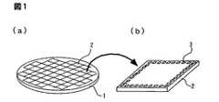
本明細書中では、主な用語を次のように定義する。半導体装置とは、その形態に関わらず、回路が形成されたウエハ状態のもの(例えば、図1(a))であっても、半導体素子(例えば、図1(b))であっても、その後パッケージされたもの(QFP、BGA、CSP等)であっても構わない。尚、図1は被検査対象の一例であり、電極3の配列は、周辺電極配列であるか全面電極配列であるかを問わない。プローブシートとは、被検査対象の電極と接触する接触端子とそこから引き出された配線を有するシートをいう。プローブカードとは、被検査対象の電極と接続して、測定器であるテスタと該被検査対象とを電気的に接続するコネクタとして機能する構造体(例えば、図2に示す構造体)をいう。
【0017】
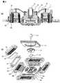
本発明に係るプローブカードの構造について図2および図3を用いて説明する。図2(a)は、本発明に係るプローブカードの第1の実施の形態の要部を示す断面図であり、図2(b)は、その主要部品を分解して図示した斜視図である。本プローブカードの第1の実施の形態は、支持部材(上部固定板)7と、該支持部材7にねじ止めされる中間板24の中央部に高さ方向に調整可能に固定され、下部先端に突起部12aを有してセンターピボットの働きをし、該突起部12aの先端を支点として可動する押し駒22を介してプローブシート6に押圧力を付与するばね12bを装填したスプリングプローブ12と、該プローブシート6の複数個の接触端子4が形成された領域を囲むように裏面に接着固定された枠21と、プローブシート6の接触端子4が形成された領域の裏面との間にシリコーンシートなどの緩衝材23および押し駒22を中央部に有し、該枠21にねじ止めされる中間板24とを含み構成される。そして、この支持部材7は、該支持部材7に設けられた平行出し調整ねじ25により、プローブカードの接触端子4の面と半導体素子の対応する電極面の平行出しが実施される。
【0018】
本プローブカードでは、中間板24の中央部に設置したスプリングプローブ12の先端の突起部12aにより微傾動可能に保持された押し駒22に対し、該スプリングプローブ12により所望のほぼ一定の押し付け力(例えば、500ピン程度の場合、押し込み量150μmで20N程度)を付与する(押圧する)ことにより、複数個の接触端子が形成された領域に所望のほぼ一定の押し付け力を付与する構造の、コンプライアンス機構を用いている。なお、押し駒22の上面中央部に突起部12aと係合する円錐溝22aが形成されている。
【0019】
上記プローブシート6は、図2(a)(b)に示すように、シートのプロービング側の中央領域部に半導体素子2の電極群3と接触するための複数個の接触端子4を形成し、該接触端子4の周囲を二重に囲むように金属膜30aおよび枠21に対応した領域に金属膜30bを形成し、プローブシート6の4辺の周辺部に多層配線基板50との信号授受のための複数個の周辺電極5を形成し、該周辺電極5を囲むように周辺電極固定板9に対応した領域に金属膜30cを形成し、該接触端子4と周辺電極5との間に多数の引き出し配線20を形成したプローブシート6で形成される。更に、上記接触端子4を形成した領域のプローブシート6の裏面には、枠21が接着固定され、信号授受のためのプローブシート6の周辺電極5を形成した部分の裏面には、周辺電極固定板9が接着固定される。更に、上記枠21は、中間板24にねじ止めされる。この中間板24には、スプリングプローブ12が固定され、下部先端の突起部12aが、押し駒22の上面中央に形成された円錐溝22aと係合するように構成される。
【0020】
なお、金属膜30aは、図3bに示したように、複数個の接触端子4の群の中央部に間隔がある場合は、中央部にも金属膜30dを形成してもよい。また、金属膜30cには、位置決め用のノックピン用孔30eおよびねじ挿入用孔30fをパターン形成しておくことにより、組み立て性を向上することができる。
【0021】
例えば、図13に示したように、金属膜30cの位置決め用のノックピン用孔30eおよび多層配線基板50の対応するノックピン用孔50eおよび下押さえ板33のノックピン用孔33eおよび周辺電極固定板9のノックピン用孔9eを用いて、ノックピン34により全体を位置決めして、周辺電極固定板9を下押さえ板33にねじ止め固定する。次に、プローブシート6に周辺電極5の群を囲むように固着した周辺電極固定板9に緩衝材31をはさんで周辺押さえ板32を、周辺電極固定板9のノックピン用孔9eおよび周辺押さえ板32のノックピン用孔32eを用いてノックピン34で位置決めして、下押さえ板33にねじ止め固定することにより、緩衝材31を介して周辺電極5の群を多層配線基板50の電極50aに押し付けて接続する。
【0022】
ここで、プローブシート6の接触端子4の群を二重に取り囲むように円状の金属膜30aおよび(枠21に対応した領域に)金属膜30bを形成することにより、内側の金属膜30aで、該接触端子群の位置精度を確保し、枠21に対応した領域に形成した金属膜30bとその内側の金属膜30aとの間の金属膜30のない柔軟性を有したプローブシート領域で、接触対象のウエハ面の微妙な傾きに金属膜で裏打ちされた部分を保ったまま倣い動作ができる構造が実現可能となる。すなわち、複数の接触端子4が金属膜30aで取り囲むことで、検査動作時に該接触端子が形成された領域に余分な応力が加わるのを防ぐことができ、従って被検査対象の電極との精確な接触が実現できる。加えて、金属膜30を、42アロイあるいはインバーなどのシリコンウエハとほぼ同程度の線膨張率を持った材料を使用することにより、被検査対象(シリコンウエハ)とほぼ一致することができ、高温時でも接触端子先端の位置精度を確保することができる。
【0023】
また、前記したようにプローブシート6の周辺部の周辺電極5の群を囲むように周辺電極固定板9に対応した領域に金属膜30cを形成することにより、プローブシート6の強度を確保でき、該周辺電極群の位置精度を確保することができ、組み立て時の取り扱いも容易となる。加えて、金属膜30cにホトリソマスクによる一括エッチング処理で、位置精度および形状が正確な位置決め用孔およびねじ挿入孔を形成することにより、組み立て作業を容易にすることができる。
【0024】
次に、本発明に係る接続装置の第2の実施の形態を図3を用いて説明する。図3(a)は、本発明に係る接続装置の第2の実施の形態の要部を示す断面図であり、図3(b)は、その主要部品を分解して図示した斜視図である。本接続装置の第2の実施の形態における第1の実施の形態と相違する点は、押し駒22に押圧力を付与する手段として、スプリングプローブ12にかえてスプリングプランジャ13および突起状の押さえピン14を用いる点、あるいは該スプリングプランジャ13を固定した中間板24と、支持部材7とを板ばね15で可動な状態で保持する構造を用いる点、あるいは金属膜30aの接触端子群4の中央部に間隔がある場合は、中央部にも金属膜30dを形成する点にある。いずれの変更も、第1の実施の形態の例で開示した構造と必要に応じて組み合わせて実施可能である。
【0025】
尚、所望のほぼ一定の押し付け力を付与するコンプライアンス機構は、上記実施の形態に限らず、種々変更してもよい。
【0026】
次に、前記プローブカードにて用いられるプローブシート(構造体)の一例について、その製造方法を図4を参照して、説明する。
【0027】
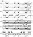
図4は、図2に示すプローブカードを形成するための製造プロセスのうち、特に、型材であるシリコンウエハ80に異方性エッチングで形成した角錐台状の穴を型材として用いて、角錐台状の接触端子先端部および引き出し配線20をポリイミドシートと一体で形成し、該ポリイミドシートに金属膜をポリイミド接着シートで接合し、該金属膜に補強板および位置決め用ノックピン孔としてエッチング加工して形成したプローブシート6を形成する製造プロセスを工程順に示したものである。
【0028】
まず図4(a)に示す工程が実行される。この工程は、厚さ0.2〜0.6mmのシリコンウエハ80の(100)面の両面に熱酸化により二酸化シリコン膜81を0.5μm程度形成し、ホトレジストを塗布し、フォトリソグラフィ工程により角錐台状の穴をあける位置のホトレジストを除去したパターンを形成した後、該ホトレジストをマスクとし、二酸化シリコン膜81をフッ酸とフッ化アンモニウムの混合液によりエッチング除去して、前記二酸化シリコン膜81をマスクとして、シリコンウエハ80を強アルカリ液(例えば、水酸化カリウム)により異方性エッチングして、(111)面に囲まれた角錐台状のエッチング穴80aを形成する工程が実行される。
【0029】
ここで、本実施例ではシリコンウエハ80を型材としたが、型材としては、結晶性を有するものであればよく、その範囲で種々変更可能であることは言うまでもない。また、本実施例では異方性エッチングによる穴を角錐台状としたが、その形状は、角錐状でもよく、小さな針圧で安定した接触抵抗を確保できる程度の接触端子4を形成できる形状の範囲で、種々変更可能である。また、接触対象とする電極に、複数の接触端子で接触するようにしてもよいことはいうまでもない。
【0030】
次に、図4(b)に示す工程が実行される。この工程はマスクとして用いた二酸化シリコン膜81をフッ酸とフッ化アンモニウムの混合液によりエッチング除去して、再度シリコンウエハ80の全面を、ウェット酸素中での熱酸化により、二酸化シリコン膜82を、0.5μm程度形成し、その表面に導電性被覆83を形成し、次に該導電性被覆83の表面に、ポリイミド膜84を形成し、ついで、接触端子4を形成すべき位置にあるポリイミド膜84を、上記導電性被覆83の表面に至るまで除去する工程が実行される。
【0031】
上記導電性被覆83としては、例えば、クロムをスパッタリング法あるいは蒸着法により成膜することにより、厚さ0.1μm程度のクロム膜を形成して、該クロム膜を形成した表面に銅をスパッタリング法あるいは蒸着法により成膜することにより、厚さ1μm程度の銅膜を形成すればよい。該銅膜に数μm厚の銅をめっきで形成して、レーザ加工の耐性を増してもよい。上記ポリイミド膜84を除去するには、例えば、レーザ穴あけ加工あるいはポリイミド膜84の表面にアルミニウムマスクを形成してドライエッチングを用いればよい。
【0032】
次に、図4(c)に示す工程が実行される。まず、該ポリイミド膜84の開口部に露出した導電性被覆83に、該導電性被覆83を電極として、硬度の高い材料を主成分として電気めっきして、接触端子4および接続電極部4bを一体として形成する。硬度の高いめっき材料として、例えば、ニッケル8a、ロジウム8b、ニッケル8cを順次にめっきして接触端子4および接続電極部4bを一体として接触端子部8を形成すればよい。
【0033】
次に、上記の接触端子部8およびポリイミド膜84に導電性被覆86を形成し、ホトレジストマスク87を形成した後、配線材料88をめっきする。
【0034】
上記導電性被覆として、例えば、クロムをスパッタリング法あるいは蒸着法により成膜することにより、厚さ0.1μm程度のクロム膜を形成して、該クロム膜を形成した表面に銅をスパッタリング法あるいは蒸着法により成膜することにより、厚さ1μm程度の銅膜を形成すればよい。また、配線材料としては、銅を用いればよい。
【0035】
次に、図4(d)に示す工程が実行される。この工程は上記ホトレジストマスク87を除去し、配線材料88をマスクとして導電性被覆86をソフトエッチング除去した後、接着層89および金属膜30を形成し、該金属膜30にホトレジストマスク91を形成するものである。
【0036】
ここで、接着層89としては、例えば、ポリイミド系接着シートあるいは、エポキシ系接着シートを用いればよい。また、金属膜30として、42アロイ(ニッケル42%および鉄58%の合金で線膨張率4ppm/℃)あるいはインバー(例えば、ニッケル36%および鉄64%の合金で線膨張率1.5ppm/℃)の様な低線膨張率で、かつシリコンウエハ(シリコン型材)80の線膨張率に近い金属シートを、接着層89で配線材料88を形成したポリイミド膜84に貼り合わせて構成することにより、形成されるプローブシート6の強度向上、大面積化が図れるほか、検査時の温度による位置ずれ防止等、様々な状況下での位置精度確保が可能である。この主旨において、金属膜30としては、バーンイン検査時の位置精度確保をねらい、被検査対象の半導体素子の線膨張率に近い線膨張率の材料を用いてもよい。
【0037】
上記接着工程は、例えば、接触端子部8および配線材料88を形成したポリイミド膜84を形成したシリコンウエハ80と、接着層89および金属膜30を重ね合わせて、10〜200Kgf/cm2で加圧しながら接着層89のガラス転移点温度(Tg)以上の温度を加え、真空中で加熱加圧接着すればよい。
【0038】
次に、図4(e)に示す工程が実行される。この工程は、上記ホトレジストマスク91により金属膜30をエッチングした後、プロセスリング95を前記金属膜30に接着剤96で固着し、該プロセスリング95に保護フィルム97を接着した後、中央をくりぬいた保護フィルム98をマスクとして二酸化シリコン82をフッ酸とフッ化アンモニウムの混合液によりエッチング除去するものである。金属膜30として、42アロイシートあるいはインバーシートを用いた場合は、塩化第二鉄溶液でスプレーエッチングすればよい。また、ホトレジストマスクとしては、液状レジストでもフィルム状レジスト(ドライフィルム)でもよい。
【0039】
次に、図4(f)に示す工程が実行される。この工程は上記保護フィルム97および98を剥離し、シリコンエッチング用保護治具100を取り付けて、シリコンをエッチング除去するものである。例えば、中間固定板100dに、前記プロセスリング95をねじ止めして、ステンレス製の固定治具100aとステンレス製のふた100bとの間にOリング100cを介して装着し、型材であるシリコンウエハ80を強アルカリ液(例えば、水酸化カリウム)によりエッチング除去すればよい。
【0040】
次に、図4(g)に示す工程が実行される。この工程は上記シリコンエッチング用保護治具100を取り外し、図4(d)と同様にプロセスリング95に保護フィルムを接着し、二酸化シリコン82および導電性被覆83(クロムおよび銅)およびニッケル8aをエッチング除去し、保護フィルムを除去した後、プローブシートの枠21と金属膜30bとの間、および周辺電極固定板9と金属膜30cとの間に接着剤96bを塗布して、金属膜30の所定の位置に固着するものである。
二酸化シリコン膜82は、フッ酸とフッ化アンモニウムの混合液によりエッチング除去し、クロム膜を過マンガン酸カリウム液によりエッチング除去し、銅膜およびニッケル膜8aをアルカリ性銅エッチング液によりエッチング除去すればよい。
なお、この一連のエッチング処理の結果、接触端子表面に露出するロジウムめっき8bを用いるのは、電極3の材料であるはんだやアルミニウム等が付きにくく、ニッケルより硬度が高く、酸化されにくく接触抵抗が安定なためである。
【0041】
次に、上記のプローブシート枠21および周辺電極固定板9の外周部に沿って一体となったポリイミド膜84および接着層89を切り出すことで、図4(h)のように、プローブカード105に取り付けられるプローブシートになる。
【0042】
次に、上記プローブシートとは製造工程が若干異なる第二の形態のプローブシートの製造方法について、図5を参照して、その製造工程を説明する。
【0043】
図5(a)〜(e)は、プローブシートを形成する他の製造プロセスを工程順に示したものである。
【0044】
まず図4(a)に示したシリコンウエハ80に角錐状のエッチング穴80aを形成し、その表面に二酸化シリコン膜82を形成し、その上に形成した導電性被覆83の表面に、接続端子部8を開口するようにホトレジストマスク85を形成する工程が実行される。
【0045】
次に、図5(b)に示す上記ホトレジストマスク85をマスクとして、上記導電性被覆83を給電層として電気めっきして、接触端子4aおよび接続電極部4bを一体として形成し、該ホトレジストマスク85を除去する工程が実行される。めっき材料として、例えば、ニッケル8a、ロジウム8b、ニッケル8cを順次にめっきして接触端子4aおよび接続電極部4bを一体として接触端子部8を形成すればよい。
【0046】
次に、図5(c)に示す工程が実行される。この工程は、上記接触端子部8および導電性被覆83を覆うようにポリイミド膜84bを形成し、上記接触端子部8からの引き出し配線接続用穴を形成すべき位置にある該ポリイミド膜84bを、上記接触端子部8の表面に至るまで除去し、該ポリイミド膜84bに導電性被覆86を形成し、ホトレジストマスク87を形成した後、配線材料88をめっきするものである。
上記ポリイミド膜84bの一部を除去するには、例えば、レーザ穴あけ加工あるいはポリイミド膜84bの表面にアルミニウムマスクを形成してドライエッチングを用いればよい。
上記導電性被覆として、例えば、クロムをスパッタリング法あるいは蒸着法により成膜することにより、厚さ0.1μm程度のクロム膜を形成して、該クロム膜を形成した表面に銅をスパッタリング法あるいは蒸着法により成膜することにより、厚さ1μm程度の銅膜を形成すればよい。また、配線材料としては、銅めっきあるいは、銅めっきにニッケルめっきをした材料を用いればよい。
【0047】
次に、図5(d)に示す工程が実行される。この工程は、上記ホトレジストマスク87を除去し、配線材料88をマスクとして導電性被覆86をエッチング除去した後、接着層89および金属膜90を接着し、ホトレジストマスクで該金属膜90をエッチングして所望の金属膜のパターンを形成するものである。
【0048】
次に、図4(e)〜(g)と同様な工程を経て、図5(e)に示すように、プローブカード105に取り付けられるプローブシートになる。
【0049】
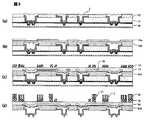
第三の形態のプローブシートの製造方法について、図6を参照して、その製造工程を説明する。
【0050】
本プローブシートの製造方法は、初期的に選択エッチング用のめっき膜を形成する点以外は、図4、図5で記述したプローブシートの製造方法と同様である。該選択めっき膜61は、接触端子の高さ(ポリイミド膜からの突出量)を確保するために用いるものである。本製造工程では、異方性エッチングによる穴を型材として接触端子を作成する場合でも、狭ピッチかつ高密度の接触端子を維持しつつ、その高さを独立、かつ自由に調整することができます。
【0051】
上記の選択めっき膜61を用いてプローブシートを形成する製造方法の一例について図6を用いて次に説明する。
【0052】
まず、図6(a)に示す工程が実行される。この工程は、図4(a)、図4(b)と同様な工程で、シリコンウエハ80に角錐状のエッチング穴を形成し、その表面に二酸化シリコン膜82および導電性被覆83を形成し、図4(b)とは異なり、接触端子部8を形成する部分に、ホトレジスト60あるいはドライフィルムのパターンを形成する。
【0053】
次に、図6(b)に示す工程が実行される。前記の導電性被覆83を電極として、選択めっき膜61をめっきする。選択めっき膜61としては、例えば、銅を10〜50μmめっきする。
【0054】
次に、図6(c)に示す工程が実行される。この工程は、ホトレジスト60および選択めっき膜(銅めっき層)61の表面にクロム膜を形成し、その表面にポリイミド膜62を形成し、該ポリイミド膜62の表面にアルミニウムマスク63を形成する工程が実行される。ここで、厚さ0.1μm程度のクロム膜を形成するのは、工程上でポリイミドとの接着性を確保するためであり、クロム膜を省略することも可能である。
【0055】
次に、図6(d)に示す工程が実行される。この工程は、前記ポリイミド膜62の表面に形成したアルミニウムマスク63により、レーザあるいはドライエッチでポリイミド膜62およびホトレジスト60を、接触端子部8を形成する部分に対応する部分を除去する工程が実行される。
【0056】
次に、図6(e)に示す工程が実行される。この工程は、前記アルミニウムマスク63を除去して、導電性被覆83および選択めっき膜61を電極として、硬度の高い材料を主成分として電気めっきして、接触端子4aおよび接続電極部4bを一体として形成するものである。硬度の高いめっき材料として、例えば、ニッケル8a、ロジウム8b、ニッケル8cを順次にめっきして接触端子4aおよび接続電極部4bを一体として接触端子部8を形成すればよい。
【0057】
次に、図4(c)〜図4(d)と同様な工程で、図6(f)に示した引き出し配線88および所望の金属膜30のパターンを形成する。
【0058】
次に、図4(e)〜図4(g)と同様な工程で、図6(g)に示したプローブシートを形成する。
【0059】
第四の形態のプローブシートの製造方法について、図7を参照して、その製造工程を説明する。
【0060】
本プローブシートの製造方法は、接触端子の高さ(ポリイミド膜からの突出量)を確保するため、図6と同様に初期的に選択エッチング用のめっき膜を形成する点以外は、図4、図5で記述したプローブシートの製造方法と同様である。図6で示した工程と異なる点は、接触端子部8を形成する部分に形成したホトレジスト60を除去して、ポリイミドで接触端子部も一体的に充填する製法とする点である。
【0061】
上記の選択めっき膜61を用いてプローブシートを形成する製造方法の一例について図7を用いて次に説明する。
【0062】
まず、図7(a)に示す工程が実行される。この工程は、図6(a)、図6(b)と同様な工程で、シリコンウエハ80に角錐状のエッチング穴を形成し、その表面に二酸化シリコン膜82および導電性被覆83を形成し、接触端子部8を形成する部分に、ホトレジスト60あるいはドライフィルムのパターンを形成し、該導電性被覆83を電極として、選択めっき膜61をめっきする。その後、ホトレジスト60を上記導電性被覆83の表面に至るまですべて除去して、その後、クロム膜64を形成し、ポリイミド62aで接触端子部も一体的に充填したポリイミド膜を形成する。この場合、クロム膜を省略することも可能である。
【0063】
次に、図6(d)〜図6(g)と同様な工程で、図6(g)に示したプローブシートを形成する。
【0064】
なお、図7(c)および図7(d)に示したように、金属膜をマスクとして、ポリイミド接着層およびポリイミド膜をレーザあるいはドライエッチング等で接触端子部周辺を除去して、金属膜で補強され、接触端子部が配線材料で支持された両持ち梁あるいは、図7(e)に示したように、片持ち梁を形成してもよい。これらの両持ち梁あるいは、片持ち梁構造により、接触端子の接触面の高さばらつき吸収量が大きくできる。これらの両持ち梁あるいは片持ち梁の構造は、他のプローブシートの製造法でも同様に形成してもよいことはいうまでもない。
【0065】
第5の形態のプローブシートの製造方法について、図8を参照して、その製造工程を説明する。
【0066】
本プローブシートの製造方法は、ホトレジスト65を用いて接触端子部8を形成し、一旦、該ホトレジスト65を除去して接触端子部8を露出し、ポリイミド膜84bで覆った後、ポリイミド膜84bの一部を除去して引き出し配線88を形成する点以外は、図6で記述したプローブシートの製造方法と同様である。
【0067】
上記の製造方法の一例について図8を用いて次に説明する。
【0068】
まず、図8(a)に示す工程が実行される。この工程は、図6(a)〜図6(e)と同様な工程で、選択めっき膜61表面のホトレジスト65のパターンを用いて、シリコンウエハ80に形成した角錐状のエッチング穴を型材として、接触端子部8を形成する。ここで図6cのポリイミド膜62あるいは図7bのポリイミド膜62aにかえて、除去が容易なホトレジスト65を用いることが望ましい。
【0069】
次に、図8(b)に示す工程が実行される。この工程は前記のホトレジスト65を除去して、接触端子部8のシリコンウエハ80の反対面を露出し、ポリイミド膜84bで覆った後、アルミニウムマスク63aを形成するものである。
【0070】
次に、図8(c)に示す工程が実行される。この工程は前記アルミニウムマスク63aを用いて引き出し配線88と接続する部分のポリイミド膜84bを接触端子部8の表面に至るまで除去し、その後、図6(f)と同様の工程で、引き出し配線および接着層89および金属膜30のパターンを形成するものである。
【0071】
次に、図4(e)〜図4(g)と同様な工程で、図8(d)に示したプローブシートを形成する。
【0072】
以上、プローブシートの製造方法について幾つか述べたが、その工程は必要に応じて適宜組合せ可能である。
【0073】
なお、高速電気信号検査用のプローブとして電気信号の乱れを極力防止するためには、プローブシートの表面(両表面あるいは一方の面)あるいは、グランド層を挟んだプローブシート構造とすればよい。例えば、金属膜のパターンを形成した面に導電材料のスパッタ膜を形成する。スパッタ膜材料としては、クロム、チタン、銅、金、ニッケルなどを単独、あるいは組み合わせて用いればよい。
【0074】
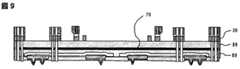
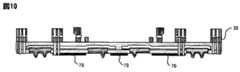
また、金属膜30を可能な限り残して、グランド層70として利用することも可能である。また、図9に示したように、銅膜を引き出し配線20の上の接着層89と金属膜30との間に多層膜として形成し、グランド層70として用いてもよい。また、図10に示したように、例えば、図4(f)の直後にシリコンウエハ80をエッチング除去して、表面に導電性被覆83が露出した段階で、ホトレジストマスクを形成して導電性被覆83でグランド層70を形成することも可能である。
【0075】
以上、プローブシートのグランド層の形成方法については、前述の図4〜図8のどの製法のプローブカードにも適用できることは言うまでもない。
【0076】
より高速の電気信号検査を可能にするために、接触端子の近傍に、電気信号の乱れを防止する目的で、コンデンサあるいは抵抗器などの搭載部品72を設置するためのプローブシート6の一例を、図14に示した。図14(a)にグランド層70および電源層71をシート状にして、逐次積層形成したプローブシート6に搭載部品72を接続した断面図、図14(b)に、プローブシート6表面に搭載部品72を接続した平面概略図を示した。例えば、図14(b)のような状態でプローブシート6に搭載部品72を接続する場合は、グランド用および電源用配線の配線幅を可能な限り広くして配線抵抗値を下げ、グランド配線と電源配線が隣同士(ペア線)になるように配置し、各々の配線に搭載する部品の接続用電極となる部分の絶縁層を、レーザあるいはドライエッチングなどの穴あけ加工技術を用いて穴あけ加工して、ビア形成用穴72aを設け、その穴に、はんだあるいはめっきなどの導電材料72bを充填して、はんだ接合あるいは金属拡散接合などで搭載部品72をプローブシート6に接合すればよい。
【0077】
プローブシート6の周辺電極5の群を、多層配線基板50の表面に形成した電極群50aに導通させるための該周辺電極群5のパターンおよびそれに対応する多層配線基板50の該電極群50aのパターンの一例を、図15に示した。
【0078】
プローブシート6の配線20および周辺電極5は、例えば、図4〜図8の製造プロセスによる薄膜配線形成により、ポリイミドシートの一方の面に接触端子が突出した形で形成され、ポリイミド内部に配線20が形成される。そのため、配線20がポリイミドで覆われるため、多層配線基板50の表面に形成した電極群50aに配線20が接触することがなく、短絡することがない構成である。このプローブシート6の周辺電極5の群を、スルーホールビア50dで多層配線基板50の内部配線50bに接続された電極群50aに、前述したノックピン34を用いて位置決めして、緩衝材31を挟んで周辺押さえ板で押さえ込むことにより、両電極を圧接する。
【0079】
ここで、個別の電極50aに対して、プローブシート6の周辺電極5を複数個形成するのは、接触面の異常や異物、凹凸などによる接触不良の可能性を少なくして、安定した接触を確保するためである。個々の周辺電極5に複数個の接触端子を設けるのは、電極の寸法に余裕がある場合に形成すればよいのであり、1個であってもよいことは、いうまでもない。
【0080】
ここで、図4〜図8の製造プロセスによるプローブシート6を形成する場合、周辺電極5を角錐形状あるいは角錐台形状等の接触端子とすることができるため、従来の半球状めっきバンプや平面電極同士の接触と比較して、硬度のある接触端子で低接触圧で安定した接触特性値が実現でき、また、ホトリソ工程で形成するため、先端位置精度が良好な接続を実現できる。上記理由により先端位置精度が良好であることから、位置決め用孔による位置合わせだけで、多層配線基板50の電極群50aとの正確な接続が容易に実現できる。なによりも、多層配線基板の電極群50aに接続するための周辺電極5を、ウエハ電極接続用の接触端子4と共に同一面側に一括形成することができ、効率的である。
【0081】
次に、以上説明した本発明に係るプローブカードを用いた半導体検査装置について図11を用いて説明する。
【0082】
図11は、本発明に係る半導体検査装置を含む検査システムの全体構成を示す図である。図11は、所望の荷重をウエハ1の面に加えて電気特性検査を実施する試験装置を示す。この状態では、スプリングプローブ12の荷重が全接触端子に加わり、ウエハ1の電極3に接触した接触端子4、引き出し配線20、周辺電極5、配線基板50の電極50a、内部配線50b、接続端子50cを通じて半導体素子の電気的特性の検査を行うテスタ(図示せず)との間で検査用電気信号の送受信が実施される。
【0083】
検査システムの全体構成において、プローブカードはウエハプローバとして構成されている。この検査システムは、被検査対象である半導体ウエハ1を支持する試料支持系160と、被検査対象(ウエハ)1の電極3に接触して電気信号の授受を行うプローブカード120と、試料支持系160の動作を制御する駆動制御系150と、被検査対象1の温度制御を行う温度制御系140と、半導体素子(チップ)2の電気的特性の検査を行うテスタ170とで構成される。この半導体ウエハ1は、多数の半導体素子(チップ)が配列され、各半導体素子の表面には、外部接続電極としての複数の電極3が配列されている。試料支持系160は、半導体ウエハ1を着脱自在に載置してほぼ水平に設けられた試料台162と、この試料台162を支持するように垂直に配置される昇降軸164と、この昇降軸164を昇降駆動する昇降駆動部165と、この昇降駆動部165を支持するX−Yステージ167とで構成される。X−Yステージ167は、筐体166の上に固定される。昇降駆動部165は、例えば、ステッピングモータなどから構成される。試料台162の水平および垂直方向における位置決め動作は、X−Yステージ167の水平面内における移動動作と、昇降駆動部165による上下動などとを組み合わせることにより行われる。また、試料台162には、図示しない回動機構が設けられており、水平面内における試料台162の回動変位が可能にされている。
【0084】
試料台162の上方には、プローブ系120が配置される。すなわち、例えば、図2に示すプローブカード120および多層配線基板50は、当該試料台162に平行に対向する姿勢で設けられる。各々の接触端子4は、該プローブカード120のプローブシート6に設けられた引き出し配線20、周辺電極5を介して、多層配線基板50の電極50aおよび内部配線50bとを通して、該配線基板50に設けられた接続端子50cに接続され、該接続端子50cに接続されるケーブル171を介して、テスタ170と接続される。
【0085】
ここで、ヒータにより所望の温度に加熱されたウエハと該ウエハの電極に接触して電気信号検査を実施するための接触端子を形成したプローブシートの温度差による位置ずれを防止し、位置合わせを精確にしかも短時間に実施するため、プローブシートあるいはプローブカードの表面あるいは内部にあらかじめ温度制御の可能な発熱体を形成しておいてもよい。発熱体としては、例えば、Ni-Crのような抵抗値の高い金属材料や高抵抗の導電樹脂を直接プローブシートあるいは多層配線基板層に形成したり、該材料を形成したシートをプローブシートにはさんだり、プローブカードに貼り付けてもよい。また、発熱体として暖めた液体をヒートブロック内のチューブに流して該ヒートブロックをプローブカードに接触させてもよい。
【0086】
加熱されたウエハからの熱放射と、プロービング時の接触からプローブカードの温度が決まる従来方法と異なり、上記のようにプローブシートを独立して検査時の温度に保っておくことにより、ウエハとプローブシート間の検査時の温度差の発生を防止することができ、位置精度の精確なプロービングが可能となる。
【0087】
駆動制御系150は、ケーブル172を介してテスタ170と接続される。また、駆動制御系150は、試料支持系160の各駆動部のアクチュエータに制御信号を送って、その動作を制御する。すなわち、駆動制御系150は、内部にコンピュータを備え、ケーブル172を介して伝達されるテスタ170のテスト動作の進行情報に合わせて、試料支持系160の動作を制御する。また、駆動制御系150は、操作部151を備え、駆動制御に関する各種指示の入力の受付、例えば、手動操作の指示を受け付ける。
【0088】
試料台162には、半導体素子2を加熱させるためのヒータ141が備えられている。温度制御系140は、試料台162のヒータ141あるいは冷却治具を制御することにより、試料台162に搭載された半導体ウエハ1の温度を制御する。また、温度制御系140は、操作部151を備え、温度制御に関する各種指示の入力の受付、例えば、手動操作の指示を受け付ける。ここで、上記プローブシートあるいはプローブカードの一部に設けた温度制御の可能な発熱体と試料台162のヒータ141とを連動させて温度制御してもよい。
【0089】
以下、半導体検査装置の動作について説明する。まず、被検査対象である半導体ウエハ1は、試料台162の上に位置決めして載置され、X−Yステージ167および回動機構を駆動制御し、半導体ウエハ1上に配列された複数個の半導体素子上に形成された電極3の群を、プローブカード120に並設された多数の接触端子4の直下に位置決めする。その後、駆動制御系150は、昇降駆動部165を作動させて、多数の電極(被接触材)3の全体の面が接触端子の先端に接触した時点から30〜100μm程度押し上げる状態になるまで試料台162を上昇させることによって、プローブシート6において多数の接触端子4が並設された領域部4aを張り出させて平坦度を高精度に確保された多数の接触端子4における各々の先端を、コンプライアンス機構(押圧機構)により半導体素子に配列された多数の電極3の群(全体)の面に追従するように倣って平行出しすることによって半導体ウエハ1上に配列された各被接触材(電極)3に倣って均一な荷重(1ピン当たり3〜150mN程度)に基づく押し込みによる接触が行われ、各接触端子4と各電極3との間において低抵抗(0.01Ω〜0.1Ω)で接続されることになる。
【0090】
さらに、ケーブル171、配線基板50、および接触端子4を介して、半導体ウエハ1に形成された半導体素子とテスタ170との間で、動作電流や動作検査信号などの授受を行い、当該半導体素子の動作特性の可否などを判別する。さらに、上記の一連の検査動作が、半導体ウエハ1に形成された複数の半導体素子の各々について実施され、動作特性の可否などが判別される。
【0091】
最後に、上記半導体検査装置を用いた検査工程、又は検査方法を含む、半導体装置の製造方法について図12を参照して説明する。
【0092】
本発明に係る半導体装置の製造方法は、ウエハに回路を作りこみ、半導体素子を形成する工程と、本発明に係る半導体検査装置によりウエハレベルで複数の半導体素子2の電気的特性を一括して検査する工程と、該ウエハをダイシングし、半導体素子ごとに分離する工程と、該半導体素子を樹脂等で封止する工程を有するものである。
【0093】
本発明に係る他の半導体装置の製造方法は、ウエハに回路を作りこみ、半導体素子を形成する工程と、本発明に係る半導体検査装置によりウエハレベルで複数の半導体素子2の電気的特性を一括して検査する工程と、該ウエハをダイシングし、半導体素子ごとに分離する工程を有するものである。
【0094】
本発明に係る他の半導体装置の製造方法は、ウエハに回路を作りこみ、半導体素子を形成する工程と、該ウエハを樹脂等で封止する工程と、該封止されたウエハに形成された複数の半導体素子2の電気的特性を本発明に係る半導体検査装置により一括して検査する工程を有するものである。
【0095】
本発明に係る他の半導体装置の製造方法は、ウエハに回路を作りこみ、半導体素子を形成する工程と、該ウエハを樹脂等で封止する工程と、該封止されたウエハに形成された複数の半導体素子2の電気的特性を本発明に係る半導体検査装置により一括して検査する工程と、該ウエハをダイシングし、半導体素子ごとに分離する工程を有するものである。
【0096】
上記した半導体装置の製造方法における該半導体素子2の電気的特性を検査する工程では、本願で開示したプローブカードを用いることにより、位置精度よく良好な接触特性を得ることができる。
【0097】
すなわち、結晶性を有する基板の異方性エッチングによる穴を型材としてめっきすることで形成される角錐形状又は角錐台形状の接触端子4を用いて検査することにより、低接触圧で安定した接触特性を実現でき、下部にある半導体素子を傷めずに検査することが可能である。また、複数の接触端子4が金属膜30aで取り囲まれる構造をとるため、検査動作時でも該接触端子は余分な応力を受けず、該半導体素子2の電極との精確な接触が実現できる。複数個の半導体素子2を一括で検査することも可能になる。
【0098】
さらに、半導体素子2の電極への圧痕は、小さく、しかも点(角錐形状又は角錐台形状に穴があいた点)になるため、該電極表面には圧痕のない平らな領域が残ることになり、図12に示すように接触による検査が複数回あっても対応できる。
【0099】
以上、本発明者によってなされた発明を実施形態に基づき具体的に説明したが、本発明は上記実施形態に限定されるものではなく、その要旨を逸脱しない範囲で種々変更可能であることはいうまでもない。
【0100】
【発明の効果】
本願において開示される発明のうち代表的なものによって得られる効果を簡単に説明すれば、下記のとおりである。
【0101】
(1)接触端子の先端位置精度を確保し、狭ピッチの電極構造を有する半導体素子を確実に検査できる検査装置を提供することができる。
【0102】
(2)電極への良好な接続を確保し、信頼性を向上させた半導体装置の製造方法を提供することができる。
【図面の簡単な説明】
【図1】(a)は、半導体素子(チップ)が配列された被接触対象であるウエハを示す斜視図であり、(b)は半導体素子(チップ)を示す斜視図である。
【図2】(a)は、本発明に係るプローブカードの第一実施例の要部を示す断面図である。
(b)は、図2の主要部品を分解して図示した斜視図である。
【図3】(a)は、本発明に係るプローブカードの第二実施例の要部を示す断面図である。
(b)は、図3の主要部品を分解して図示した斜視図である。
【図4】(a)〜(h)は、本発明に係るプローブカードにおけるプローブシート部分を形成する製造プロセスを工程順に示したものである。
【図5】(a)〜(e)は、本発明に係るプローブカードにおけるプローブシートを形成する他の製造プロセスを工程順に示したものである。
【図6】(a)〜(g)は、本発明に係るプローブカードにおけるプローブシートを形成する他の製造プロセスを工程順に示したものである。
【図7】(a)〜(c)は、本発明に係るプローブカードにおけるプローブシートを形成する他の製造プロセスを工程順に示したものであり、(d1)および(e1)は、それぞれ本発明に係るプローブカードにおけるプローブシートの接触端子部8を形成した領域の一部概略断面図を示したものであり、(d2)は、(d1)の接触端子部8を形成した領域の一部を、(d1)の下面から見た平面図であり、(e2)は、(e1)の接触端子部8を形成した領域の一部を、(e1)の下面から見た平面図である。
【図8】(a)〜(d)は、本発明に係るプローブカードにおけるプローブシートを形成する他の製造プロセスを工程順に示したものである。
【図9】図9は、本発明に係るプローブカードにおけるグランド層を形成したプローブシートの概略断面図を示したものである。
【図10】図10は、本発明に係るプローブカードにおけるグランド層を形成した他のプローブシートの概略断面図を示したものである。
【図11】本発明に係る検査システムの一実施の形態を示す全体概略構成を示す図である。
【図12】半導体装置の検査工程の一実施例を示す工程図である。
【図13】本発明に係るプローブカードの組み立て方法を示す概略図である。
【図14】(a)は、本発明に係るプローブカードの一実施例の要部を示す断面図である。
(b)は、図14の部品搭載部分の配線を拡大して図示した平面概略図である。
【図15】本発明に係る多層配線基板表面の周辺電極パターンおよびプローブシートの配線パターンの一例を示したものである。
【符号の説明】
1…ウエハ、2…半導体素子(チップ)、3…電極(被接触材)、4…接触端子、4b…接続電極部、5…周辺電極、6…プローブシート、7…支持部材、8…接触端子部、8a…ニッケル、8b…ロジウム、8c…ニッケル、9…周辺電極固定板、9e…ノックピン用孔、12…スプリングプローブ、突起部12a、12b…ばね、13…スプリングプランジャ、14…押さえピン、15…板ばね、20…引き出し配線、21…枠、22…押し駒、22a…円錐溝、23…緩衝材、24…中間板、25…平行出し調整ねじ、30…金属膜、30a…金属膜、30b…金属膜、30c…金属膜、30d…金属膜、30e…ノックピン用孔、30f…ねじ挿入用孔、31…緩衝材、32…周辺押さえ板、32e…ノックピン用孔、33…下押さえ板、33e…ノックピン用孔、34…ノックピン、50…多層配線基板、50a…電極、50b…内部配線、50c…接続端子、50d…スルーホールビア、50e…ノックピン用孔、60…ホトレジスト、60a…ホトレジスト、61…選択めっき膜、62…ポリイミド膜、62a…ポリイミド膜、63…アルミニウムマスク、63a…アルミニウムマスク、64…クロム膜、65…ホトレジスト、70…グランド層、71…電源層、72…搭載部品、72a…ビア形成用穴、72b…導電材料、80…シリコンウエハ、80a…エッチング穴、81二酸化シリコン膜、82…二酸化シリコン膜、83…導電性被覆、84…ポリイミド膜、84b…ポリイミド膜、86…導電性被覆、87…ホトレジストマスク、88…配線材料、89…接着層、91…ホトレジストマスク、95…プロセスリング、96…接着剤、96b…接着剤、97…保護フィルム、98…保護フィルム、100…シリコンエッチング用保護治具、100a…固定治具、100b…ふた、100c…Oリング、100d…中間固定板、105…プローブカード、120…プロ−ブカード、140…温度制御系、141…ヒータ、150…駆動制御系、151…操作部、160…試料支持系、162…試料台、164…昇降軸、165…昇降駆動部、166…筺体、167…X−Yステージ、170…テスタ、171…ケーブル、172…ケーブル[0001]
BACKGROUND OF THE INVENTION
The present invention relates to a probe sheet, a probe card, a semiconductor inspection apparatus, and a semiconductor device manufacturing method.
[0002]
[Prior art]
Of the semiconductor device manufacturing process performed after the semiconductor element circuit is formed on the wafer, an example of the flow of the inspection process is mainly shown in the package product, bare chip, and CSP, which are typical shipping forms of the semiconductor device, as an example. It was shown to.
[0003]
In the manufacturing process of the semiconductor device, the following three inspections are performed roughly as shown in FIG. First, it is performed in a wafer state in which a semiconductor element circuit and an electrode are formed on the wafer, and a wafer inspection for grasping a conduction state and an electric signal operating state of the semiconductor element, and then the semiconductor element is unstable at a high temperature, a high applied voltage, or the like. These include burn-in inspection for extracting a semiconductor element and selection inspection for grasping product performance before shipping a semiconductor device.
[0004]
As a prior art of an apparatus (semiconductor inspection apparatus) used for such a semiconductor device inspection, there is Patent Document 1 (hereinafter referred to as Prior Art 1). The technique includes a thin film support frame, a flexible thin film secured to the support frame, and a plurality of test probes provided in the central region of the outer surface of the thin film so as to be pressed onto the contact pads of the device being tested. A contact, a plurality of conductive traces on the membrane connecting each probe contact to the test circuit, and the membrane central region when the probe test contact is pressed onto the contact pad of the device to be tested. Self-rotating means (automatically comprising a pressure plate fixed to the inner surface of the thin film in the central region and a hemispherical pivot post whose head presses the center of the pressure plate in a pivotal manner) A leveling thin film test probe is described.
[0005]
As another prior art, there is Patent Document 2 (hereinafter referred to as Prior Art 2). In this technology, a support member and a plurality of contact terminals with a sharpened tip are provided in the probing side region, and a ground is sandwiched between a plurality of lead wires and an insulating layer that are electrically connected to each of the contact terminals. A multi-layer film having a layer, a frame fixed to the back side of the multi-layer film, a pressing member, and a contact pressure for bringing the tip of each contact terminal into contact with each electrode is applied from the support member to the pressing member. And a compliance mechanism in which when the tip surface of the contact terminal group is brought into contact with the surface of the electrode group, the tip surface of the contact terminal group projects parallel to the surface of the electrode group. And an inspection system that performs an inspection by bringing the connection device into contact with an electrode of an object to be inspected.
[0006]
[Patent Document 1]
Japanese Patent Application Laid-Open No. 7-7056 (Japanese Patent Application No. 6-28200)
[Patent Document 2]
Japanese Patent Laid-Open No. 11-23615 (Japanese Patent Application No. 10-49912)
[0007]
[Problems to be solved by the invention]
However, the
[0008]
On the other hand, in the above
[0009]
As described above, in any of the conventional techniques, probing corresponding to the narrow pitch multi-pin accompanying the increase in the density of the test object such as a semiconductor element can be performed without damaging the test object and the contact terminal. It was unsatisfactory with respect to the point of trying to realize a system that secures the positional accuracy of the contact terminal tip, is stable at a low load, and is easy to assemble.
[0010]
In addition, with the recent high integration of semiconductor elements, the pitch of electrodes (for example, about 0.1 mm or less) and the density increase further, and in addition, the reliability can be grasped more clearly. Since an operation test at a high temperature (for example, 85 ° C. to 150 ° C.) tends to be performed, an inspection apparatus that can cope with these is desired.
[0011]
An object of the present invention is to provide an inspection apparatus capable of ensuring the tip position accuracy of a contact terminal and reliably inspecting a semiconductor element having a narrow pitch electrode structure.
[0012]
Another object of the present invention is to provide a method of manufacturing a semiconductor device that ensures good connection to peripheral electrodes and has improved reliability.
[0013]
Another object of the present invention is to provide a method for manufacturing a semiconductor device that reduces the manufacturing cost of the entire semiconductor device by improving the sheet mounting property, suppressing the assembly cost of the inspection device, and reducing the cost of the inspection process of the semiconductor device. Is to provide.
[0014]
[Means for Solving the Problems]
In order to achieve any of the above objects, the outline of a representative one of the inventions disclosed in the present application will be briefly described as follows.
(1) A probe sheet having a plurality of contact terminals that come into contact with electrodes provided on an object to be inspected, wirings drawn from the contact terminals, and a plurality of peripheral electrodes electrically connected to the wirings The probe terminal is characterized in that the contact terminal and the peripheral electrode have a pyramid shape or a truncated pyramid shape.
(2) A probe sheet having a plurality of contact terminals in contact with electrodes provided on the object to be inspected, wirings drawn from the contact terminals, and a plurality of peripheral electrodes electrically connected to the wirings A probe sheet comprising: a first metal film formed so as to surround the plurality of contact terminals; and a second metal film formed so as to surround the first metal film. .
(3) A probe card having a multilayer wiring board having a plurality of contact terminals in contact with the electrodes provided on the object to be inspected, wirings drawn from the contact terminals, and electrodes electrically connected to the wirings The probe card is characterized in that the electrode of the multilayer wiring board and the wiring are electrically connected via a peripheral electrode having a pyramid shape or a truncated pyramid shape.
(4) A multilayer wiring board that is electrically connected to a tester that inspects the electrical characteristics of the object to be inspected, a plurality of peripheral electrodes that are connected to the electrodes of the multilayer wiring board, and electrodes provided in the object to be inspected A probe sheet having a plurality of contact terminals in contact with each other;
Means for applying a pressing force to a region where the plurality of contact terminals of the probe sheet are formed, wherein the probe sheet is further formed so as to surround the plurality of contact terminals. The first metal film and a second metal film formed so as to surround the first metal film, and the means for applying the pressing force is formed in the region where the second metal film is formed. A probe card, wherein the probe card is disposed so that the region where the first metal film is formed and the region where the plurality of contact terminals are formed can be tilted.
(5) A semiconductor device comprising a step of forming a circuit on a wafer to form a semiconductor element, a step of inspecting the electrical characteristics of the semiconductor element, and a step of dicing the wafer and separating the semiconductor element. A plurality of contact terminals contacting the electrodes of the semiconductor element, and a first metal film formed so as to surround the plurality of contact terminals in the step of inspecting the electrical characteristics of the semiconductor element And a probe sheet having a second metal film formed so as to surround the first metal film, a region of the probe sheet in which the first metal film is formed, and the plurality of contact terminals are formed And a means for applying a pressing force to the formed region, and inspecting the plurality of contact terminals in contact with electrodes provided on the semiconductor element, using the probe card Law.
[0015]
DETAILED DESCRIPTION OF THE INVENTION
Hereinafter, embodiments of the present invention will be described in detail with reference to the drawings. Note that components having the same function are denoted by the same reference symbols throughout the accompanying drawings for describing the embodiment of the invention, and the repetitive description thereof is omitted.
[0016]
In this specification, main terms are defined as follows. Regardless of its form, the semiconductor device may be a wafer-formed circuit (for example, FIG. 1A) or a semiconductor element (for example, FIG. 1B). After that, it may be packaged (QFP, BGA, CSP, etc.). FIG. 1 shows an example of an object to be inspected, and it does not matter whether the arrangement of the
[0017]
The structure of the probe card according to the present invention will be described with reference to FIGS. FIG. 2A is a cross-sectional view showing the main part of the first embodiment of the probe card according to the present invention, and FIG. 2B is a perspective view showing the main components in an exploded manner. . The probe card according to the first embodiment is fixed to the center of a support member (upper fixing plate) 7 and an
[0018]
In this probe card, a desired substantially constant pressing force (desired by the spring probe 12) against the
[0019]
2 (a) and 2 (b), the
[0020]
In addition, as shown in FIG. 3B, the
[0021]
For example, as shown in FIG. 13, the
[0022]
Here, by forming a
[0023]
Further, as described above, by forming the
[0024]
Next, a second embodiment of the connection device according to the present invention will be described with reference to FIG. FIG. 3A is a cross-sectional view showing the main part of the second embodiment of the connection device according to the present invention, and FIG. 3B is a perspective view showing the main components in an exploded manner. . The second embodiment of the present connecting device is different from the first embodiment in that, as a means for applying a pressing force to the
[0025]
Note that the compliance mechanism that applies a desired substantially constant pressing force is not limited to the above-described embodiment, and various modifications may be made.
[0026]
Next, an example of a probe sheet (structure) used in the probe card will be described with reference to FIG.
[0027]
FIG. 4 shows a truncated pyramid shape using, in particular, a truncated pyramidal hole formed by anisotropic etching in a
[0028]
First, the step shown in FIG. In this process, a
[0029]
Here, in this embodiment, the
[0030]
Next, the process shown in FIG. 4B is performed. In this process, the
[0031]
As the
[0032]
Next, the process shown in FIG. 4C is performed. First, the
[0033]
Next, a conductive coating 86 is formed on the
[0034]
As the conductive coating, for example, chromium is formed by sputtering or vapor deposition to form a chromium film having a thickness of about 0.1 μm, and copper is formed on the surface on which the chromium film is formed by sputtering or vapor deposition. A copper film having a thickness of about 1 μm may be formed by film formation by the method. Further, copper may be used as the wiring material.
[0035]
Next, the process shown in FIG. 4D is performed. In this step, the
[0036]
Here, as the
[0037]
In the bonding step, for example, the
[0038]
Next, the process shown in FIG. In this step, after etching the
[0039]
Next, the process shown in FIG. In this step, the
[0040]
Next, the process shown in FIG. 4G is performed. In this step, the protective jig 100 for silicon etching is removed, a protective film is adhered to the
The
As a result of this series of etching processes, the rhodium plating 8b exposed on the contact terminal surface is not easily attached to the material of the
[0041]
Next, the
[0042]
Next, the manufacturing process of the probe sheet according to the second embodiment, which is slightly different from the above-described probe sheet, will be described with reference to FIG.
[0043]
5A to 5E show other manufacturing processes for forming the probe sheet in the order of steps.
[0044]
First, a pyramidal etching hole 80a is formed in the
[0045]
Next, using the
[0046]
Next, the step shown in FIG. In this step, the
In order to remove a part of the
As the conductive coating, for example, chromium is formed by sputtering or vapor deposition to form a chromium film having a thickness of about 0.1 μm, and copper is formed on the surface on which the chromium film is formed by sputtering or vapor deposition. A copper film having a thickness of about 1 μm may be formed by film formation by the method. As the wiring material, copper plating or a material obtained by nickel plating on copper plating may be used.
[0047]
Next, the process shown in FIG. In this step, the
[0048]
Next, through steps similar to those shown in FIGS. 4E to 4G, a probe sheet attached to the
[0049]
About the manufacturing method of the probe sheet of a 3rd form, the manufacturing process is demonstrated with reference to FIG.
[0050]
The method for manufacturing the probe sheet is the same as the method for manufacturing the probe sheet described in FIGS. 4 and 5 except that a plating film for selective etching is initially formed. The
[0051]
Next, an example of a manufacturing method for forming a probe sheet using the
[0052]
First, the process shown in FIG. In this step, a pyramidal etching hole is formed in the
[0053]
Next, the process shown in FIG. 6B is performed. The
[0054]
Next, the process shown in FIG. 6C is performed. In this step, a chromium film is formed on the surface of the photoresist 60 and the selective plating film (copper plating layer) 61, a
[0055]
Next, the process shown in FIG. 6D is performed. In this step, the
[0056]
Next, the process shown in FIG. In this step, the
[0057]
Next, in the same process as FIG. 4C to FIG. 4D, the pattern of the lead-
[0058]
Next, the probe sheet shown in FIG. 6G is formed by the same steps as those in FIGS. 4E to 4G.
[0059]
The manufacturing process of the probe sheet according to the fourth embodiment will be described with reference to FIG.
[0060]
The probe sheet manufacturing method is the same as that shown in FIG. 6 except that a selective etching plating film is initially formed in order to ensure the height of the contact terminals (amount of protrusion from the polyimide film). This is the same as the probe sheet manufacturing method described in FIG. 6 is different from the process shown in FIG. 6 in that the photoresist 60 formed on the portion where the
[0061]
Next, an example of a manufacturing method for forming a probe sheet using the
[0062]
First, the process shown in FIG. In this step, a pyramidal etching hole is formed in the
[0063]
Next, the probe sheet shown in FIG. 6 (g) is formed by the same steps as those in FIGS. 6 (d) to 6 (g).
[0064]
As shown in FIGS. 7C and 7D, using the metal film as a mask, the polyimide adhesive layer and the polyimide film are removed around the contact terminal portion by laser or dry etching, and the metal film is used. A cantilever beam reinforced and a contact terminal portion supported by a wiring material or a cantilever beam as shown in FIG. 7E may be formed. With these doubly-supported or cantilever structures, the amount of variation in the height of the contact surface of the contact terminal can be absorbed. Needless to say, the structure of these cantilever beams or cantilever beams may be similarly formed by other probe sheet manufacturing methods.
[0065]
About the manufacturing method of the probe sheet of the 5th form, the manufacturing process is demonstrated with reference to FIG.
[0066]
In this probe sheet manufacturing method, the
[0067]
Next, an example of the above manufacturing method will be described with reference to FIG.
[0068]
First, the process shown in FIG. This process is the same process as that shown in FIGS. 6A to 6E. Using the pattern of the photoresist 65 on the surface of the
[0069]
Next, the process shown in FIG. 8B is performed. In this step, the photoresist 65 is removed to expose the opposite surface of the
[0070]
Next, the process shown in FIG. 8C is performed. This step uses the
[0071]
Next, the probe sheet shown in FIG. 8D is formed by the same steps as those in FIGS. 4E to 4G.
[0072]
As mentioned above, although several manufacturing methods of the probe sheet were described, the process can be combined suitably as needed.
[0073]
In order to prevent disturbance of the electric signal as much as possible as a probe for high-speed electric signal inspection, the probe sheet surface (both surfaces or one surface) or a probe sheet structure sandwiching a ground layer may be used. For example, a sputtered film of a conductive material is formed on the surface on which the metal film pattern is formed. As the sputtered film material, chromium, titanium, copper, gold, nickel or the like may be used alone or in combination.
[0074]
It is also possible to leave the
[0075]
As mentioned above, it cannot be overemphasized that it can apply to the probe card of any manufacturing method of the above-mentioned FIGS. 4-8 about the formation method of the ground layer of a probe sheet | seat.
[0076]
An example of the
[0077]
The pattern of the
[0078]
The
[0079]
Here, forming a plurality of
[0080]
Here, when the
[0081]
Next, a semiconductor inspection apparatus using the probe card according to the present invention described above will be described with reference to FIG.
[0082]
FIG. 11 is a diagram showing an overall configuration of an inspection system including a semiconductor inspection apparatus according to the present invention. FIG. 11 shows a test apparatus that performs an electrical characteristic inspection by applying a desired load to the surface of the
[0083]
In the entire configuration of the inspection system, the probe card is configured as a wafer prober. This inspection system includes a sample support system 160 that supports a
[0084]
A
[0085]
Here, the wafer sheet heated to a desired temperature by the heater and the probe sheet on which the contact terminals for performing the electrical signal inspection in contact with the electrode of the wafer are formed are prevented from being displaced due to the temperature difference, and the alignment is performed. In order to carry out accurately and in a short time, a heating element capable of controlling the temperature may be formed in advance on the surface or inside of the probe sheet or probe card. As the heating element, for example, a metal material having a high resistance value such as Ni-Cr or a conductive resin having a high resistance value is directly formed on the probe sheet or the multilayer wiring board layer, or the sheet on which the material is formed is used as the probe sheet. You can stick it on the probe card. Alternatively, a warmed liquid as a heating element may be flowed through a tube in the heat block to bring the heat block into contact with the probe card.
[0086]
Unlike the conventional method in which the temperature of the probe card is determined from the heat radiation from the heated wafer and the contact during probing, the probe sheet is kept at the temperature at the time of inspection independently as described above, so that the wafer and the probe are maintained. It is possible to prevent the occurrence of a temperature difference during inspection between sheets, and it is possible to perform probing with accurate positional accuracy.
[0087]
The
[0088]
The sample stage 162 is provided with a
[0089]
Hereinafter, the operation of the semiconductor inspection apparatus will be described. First, the
[0090]
Furthermore, the operating current and the operation inspection signal are exchanged between the semiconductor element formed on the
[0091]
Finally, a semiconductor device manufacturing method including an inspection process or an inspection method using the semiconductor inspection apparatus will be described with reference to FIG.
[0092]
The method of manufacturing a semiconductor device according to the present invention includes a step of forming a circuit on a wafer and forming a semiconductor element, and a semiconductor inspection apparatus according to the present invention collectively collecting electrical characteristics of a plurality of
[0093]
Another method for manufacturing a semiconductor device according to the present invention includes a step of forming a circuit on a wafer and forming a semiconductor element, and a semiconductor inspection apparatus according to the present invention collectively collecting electrical characteristics of a plurality of
[0094]
In another method of manufacturing a semiconductor device according to the present invention, a circuit is formed on a wafer, a semiconductor element is formed, a step of sealing the wafer with resin or the like, and a step of forming the semiconductor device. The present invention includes a step of collectively inspecting the electrical characteristics of the plurality of
[0095]
In another method of manufacturing a semiconductor device according to the present invention, a circuit is formed on a wafer, a semiconductor element is formed, a step of sealing the wafer with resin or the like, and a step of forming the semiconductor device. The method includes a step of collectively inspecting electrical characteristics of a plurality of
[0096]
In the step of inspecting the electrical characteristics of the
[0097]
That is, stable contact characteristics at a low contact pressure can be obtained by inspecting using a
[0098]
Furthermore, since the indentation to the electrode of the
[0099]
As mentioned above, the invention made by the present inventor has been specifically described based on the embodiment. However, the present invention is not limited to the above embodiment, and various modifications can be made without departing from the scope of the invention. Not too long.
[0100]
【The invention's effect】
The effects obtained by the representative ones of the inventions disclosed in the present application will be briefly described as follows.
[0101]
(1) It is possible to provide an inspection apparatus capable of ensuring the tip position accuracy of the contact terminal and reliably inspecting a semiconductor element having a narrow pitch electrode structure.
[0102]
(2) It is possible to provide a method for manufacturing a semiconductor device that ensures good connection to electrodes and improves reliability.
[Brief description of the drawings]
FIG. 1A is a perspective view showing a wafer as a contact target in which semiconductor elements (chips) are arranged, and FIG. 1B is a perspective view showing a semiconductor element (chip).
FIG. 2 (a) is a cross-sectional view showing a main part of a first embodiment of the probe card according to the present invention.
(B) is the perspective view which decomposed | disassembled and illustrated the main components of FIG.
FIG. 3A is a cross-sectional view showing a main part of a second embodiment of the probe card according to the present invention.
(B) is the perspective view which decomposed | disassembled and illustrated the main components of FIG.
FIGS. 4A to 4H show a manufacturing process for forming a probe sheet portion in a probe card according to the present invention in the order of steps.
FIGS. 5A to 5E show another manufacturing process for forming a probe sheet in the probe card according to the present invention in the order of steps.
FIGS. 6A to 6G show other manufacturing processes for forming a probe sheet in the probe card according to the present invention in the order of steps. FIGS.
FIGS. 7A to 7C show other manufacturing processes for forming a probe sheet in the probe card according to the present invention in the order of steps, and (d1) and (e1) are respectively shown in the present invention. FIG. 2 is a partial schematic cross-sectional view of a region where the
8A to 8D show another manufacturing process for forming a probe sheet in the probe card according to the present invention in the order of steps.
FIG. 9 is a schematic cross-sectional view of a probe sheet on which a ground layer is formed in a probe card according to the present invention.
FIG. 10 is a schematic cross-sectional view of another probe sheet on which a ground layer is formed in the probe card according to the present invention.
FIG. 11 is a diagram showing an overall schematic configuration showing an embodiment of an inspection system according to the present invention.
FIG. 12 is a process diagram showing an example of an inspection process of a semiconductor device.
FIG. 13 is a schematic view showing a method for assembling a probe card according to the present invention.
FIG. 14A is a cross-sectional view showing the main part of one embodiment of a probe card according to the present invention.
(B) is the plane schematic which expanded and illustrated the wiring of the components mounting part of FIG.
FIG. 15 shows an example of a peripheral electrode pattern on the surface of a multilayer wiring board and a wiring pattern of a probe sheet according to the present invention.
[Explanation of symbols]
DESCRIPTION OF
Claims (17)
Translated fromJapanese該複数の接触端子を取り囲むように形成された第1の金属膜と、該第1の金属膜を取り囲むように形成された第2の金属膜とを有し、
該複数の周辺電極を取り囲むように形成された第3の金属膜を有し、該第3の金属膜には位置決め用の孔が設けられていることを特徴とするプローブシート。A plurality of contact terminals that are in contact with the electrodes provided on the object to be inspected, a wiring drawn from each of the contact terminals, and a plurality of peripherals that are electrically connected to the wiring and connected to the electrodes of the multilayer wiring board A probe sheet having electrodes,
A first metal film formed so as to surround the plurality of contact terminals, and a second metal film formed so as to surround the first metal film,
A probe sheet comprising a third metal film formed so as to surround the plurality of peripheral electrodes, and a positioning hole provided in the third metal film.
該接触端子及び該周辺電極は、角錐形状又は角錐台形状であり、
該複数の接触端子と該複数の周辺電極との間に、該複数の接触端子を取り囲むように形成された第1の金属膜と、該第1の金属膜を取り囲むように形成された第2の金属膜とを有し、
該複数の周辺電極を取り囲むように形成された第3の金属膜を有し、該第3の金属膜には位置決め用の孔が設けられていることを特徴とするプローブシート。A plurality of contact terminals that are in contact with the electrodes provided on the object to be inspected, a wiring drawn from each of the contact terminals, and a plurality of peripherals that are electrically connected to the wiring and connected to the electrodes of the multilayer wiring board A probe sheet having electrodes,
The contact terminal and the peripheral electrode have a pyramid shape or a truncated pyramid shape,
A first metal film formed so as to surround the plurality of contact terminals and a second metal formed so as to surround the first metal film between the plurality of contact terminals and the plurality of peripheral electrodes. A metal film of
A probe sheet comprising a third metal film formed so as to surround the plurality of peripheral electrodes, and a positioning hole provided in the third metal film.
該第1の金属膜の外周は、円状に形成されることを特徴とするプローブシート。The probe sheet according to claim 1 or 2,
The probe sheet, wherein the outer periphery of the first metal film is formed in a circular shape.
該プローブシートの該第1の金属膜と該第2の金属膜との間の領域は、該プローブシートの該第1の金属膜及び該第2の金属膜が形成された領域よりも柔軟性があることを特徴とするプローブシート。The probe sheet according to claim 1 or 2,
The region between the first metal film and the second metal film of the probe sheet is more flexible than the region where the first metal film and the second metal film of the probe sheet are formed. A probe sheet characterized by that.
該接触端子及び該周辺電極は、結晶性を有する基板の異方性エッチングによる穴を型材としてめっきすることにより形成されたものであることを特徴とするプローブシート。The probe sheet according to any one of claims 1 to 4,
The contact sheet and the peripheral electrode are formed by plating holes formed by anisotropic etching of a substrate having crystallinity as a mold material.
該周辺電極は、格子状に配置されていることを特徴とするプローブシート。The probe sheet according to claim 5,
The probe sheet, wherein the peripheral electrodes are arranged in a lattice shape.
さらに、該配線と電気的に接続されるグランド層及び電源層を有し、
該グランド層又は該電源層に接続される配線は、該グランド層と該電源層のいずれにも接続されない配線よりも、配線幅が広く形成されていることを特徴とするプローブシート。The probe sheet according to any one of claims 1 to 6,
Furthermore, it has a ground layer and a power supply layer electrically connected to the wiring,
A probe sheet, wherein a wiring connected to the ground layer or the power supply layer is formed wider than a wiring connected to neither the ground layer nor the power supply layer.
該多層配線基板の電極に接続される複数の周辺電極と被検査対象に設けられた電極と接触する複数の接触端子とを有するプローブシートと、
該プローブシートの該複数の接触端子が形成された領域に押し付け力を付与する手段とを有するプローブカードであって、
該プローブシートは、さらに、該複数の接触端子を取り囲むように形成された第1の金属膜と、該第1の金属膜を取り囲むように形成された第2の金属膜とを有し、
該押し付け力を付与する手段は、該第2の金属膜が形成された領域に対して該第1の金属膜が形成された領域及び該複数の接触端子が形成された領域が傾動可能になるように、配置され、
該プローブシートは、さらに、該複数の周辺電極を取り囲むように形成され、かつ位置決め用の孔が設けられた第3の金属膜を有し、
該多層配線基板は、さらに、位置決め用の孔を有し、
該複数の周辺電極と該多層配線基板の電極との接続は、該第3の金属膜に設けられた位置決め用の孔及び該多層配線基板に設けられた位置決め用の孔を通るピンを挿入することにより位置合わせされていることを特徴とするプローブカード。A multilayer wiring board electrically connected to a tester for inspecting the electrical characteristics of the inspected object;
A probe sheet having a plurality of peripheral electrodes connected to the electrodes of the multilayer wiring board and a plurality of contact terminals in contact with the electrodes provided on the object to be inspected;
A probe card having means for applying a pressing force to a region where the plurality of contact terminals of the probe sheet are formed,
The probe sheet further includes a first metal film formed so as to surround the plurality of contact terminals, and a second metal film formed so as to surround the first metal film,
The means for applying the pressing force can tilt the region where the first metal film is formed and the region where the plurality of contact terminals are formed with respect to the region where the second metal film is formed. Arranged, and
The probe sheet further includes a third metal film formed so as to surround the plurality of peripheral electrodes and provided with positioning holes,
The multilayer wiring board further has a positioning hole,
The connection between the plurality of peripheral electrodes and the electrode of the multilayer wiring board is performed by inserting a positioning hole provided in the third metal film and a pin passing through the positioning hole provided in the multilayer wiring board. A probe card characterized by being aligned with each other.
該多層配線基板の電極に接続される複数の周辺電極と被検査対象に設けられた電極と接触する複数の接触端子とを有するプローブシートと、
該プローブシートの該複数の接触端子が形成された領域に押し付け力を付与する手段とを有するプローブカードであって、
該接触端子及び周辺電極は、角錐形状又は角錐台形状であり、
該プローブシートは、さらに、該複数の接触端子を取り囲むように形成された第1の金属膜と、該第1の金属膜を取り囲むように形成された第2の金属膜とを有し、
該押し付け力を付与する手段は、該第2の金属膜が形成された領域に対して該第1の金属膜が形成された領域及び該複数の接触端子が形成された領域が傾動可能になるように、配置されており、
該プローブシートは、さらに、該複数の周辺電極を取り囲むように形成され、かつ位置決め用の孔が設けられた第3の金属膜を有し、
該多層配線基板は、さらに、位置決め用の孔を有し、
該複数の周辺電極と該多層配線基板の電極との接続は、該第3の金属膜に設けられた位置決め用の孔及び該多層配線基板に設けられた位置決め用の孔を通るピンを挿入することにより位置合わせされていることを特徴とするプローブカード。A multilayer wiring board electrically connected to a tester for inspecting the electrical characteristics of the inspected object;
A probe sheet having a plurality of peripheral electrodes connected to the electrodes of the multilayer wiring board and a plurality of contact terminals in contact with the electrodes provided on the object to be inspected;
A probe card having means for applying a pressing force to a region where the plurality of contact terminals of the probe sheet are formed,
The contact terminal and the peripheral electrode have a pyramid shape or a truncated pyramid shape,
The probe sheet further includes a first metal film formed so as to surround the plurality of contact terminals, and a second metal film formed so as to surround the first metal film,
The means for applying the pressing force can tilt the region where the first metal film is formed and the region where the plurality of contact terminals are formed with respect to the region where the second metal film is formed. Are arranged, and
The probe sheet further includes a third metal film formed so as to surround the plurality of peripheral electrodes and provided with positioning holes,
The multilayer wiring board further has a positioning hole,
The connection between the plurality of peripheral electrodes and the electrode of the multilayer wiring board is performed by inserting a positioning hole provided in the third metal film and a pin passing through the positioning hole provided in the multilayer wiring board. A probe card characterized by being aligned with each other.
該第1の金属膜と該第2の金属膜との間の領域は、該プローブシートの該第1の金属膜又は該第2の金属膜が形成された領域よりも柔軟性を有することを特徴とするプローブカード。The probe card according to claim 8 or 9, wherein
The region between the first metal film and the second metal film is more flexible than the region where the first metal film or the second metal film is formed on the probe sheet. Featured probe card.
該複数の周辺電極及び該多層配線基板の電極は、格子状に配置されていることを特徴とするプローブカード。The probe card according to claim 8 or 9, wherein
The probe card, wherein the plurality of peripheral electrodes and the electrodes of the multilayer wiring board are arranged in a lattice pattern.
該接触端子及び該周辺電極は、結晶性を有する基板の異方性エッチングによる穴を型材としてめっきすることにより形成されたものであることを特徴とするプローブカード。The probe card according to any one of claims 8 to 11,
The contact card and the peripheral electrode are formed by plating holes formed by anisotropic etching of a substrate having crystallinity as a mold material.
該被検査対象に設けられた電極と接触する複数の接触端子を有し、かつ該被検査対象の電気的特性を検査するテスタと電気的に接続されるプローブカードと、
を有する半導体検査装置であって、
該プローブカードは、請求項8から12のいずれかであることを特徴とする半導体検査装置。A sample stage on which the object to be inspected is placed;
A probe card that has a plurality of contact terminals that come into contact with electrodes provided on the object to be inspected, and is electrically connected to a tester that inspects the electrical characteristics of the object to be inspected;
A semiconductor inspection apparatus comprising:
13. The semiconductor inspection apparatus according to claim 8, wherein the probe card is any one of claims 8 to 12.
該半導体素子の電気的特性を検査する工程では、
該半導体素子の電極に接触する複数の接触端子と、該複数の接触端子を取り囲むように形成された第1の金属膜と、該第1の金属膜を取り囲むように形成された第2の金属膜と、該複数の周辺電極を取り囲むように形成された第3の金属膜とを有し、該第3の金属膜には位置決め用の孔が設けられているプローブシートを用い、
該プローブシートの該第1の金属膜が形成された領域及び該複数の接触端子が形成された領域に押し付け力を付与しつつ、該複数の接触端子を該半導体素子に設けられた電極に接触させて検査することを特徴とする半導体装置の製造方法。A method of manufacturing a semiconductor device, comprising: forming a circuit on a wafer to form a semiconductor element; inspecting electrical characteristics of the semiconductor element; and dicing the wafer to separate the semiconductor element. Because
In the step of inspecting the electrical characteristics of the semiconductor element,
A plurality of contact terminals in contact with the electrodes of the semiconductor element; a first metal film formed so as to surround the plurality of contact terminals; and a second metal formed so as to surround the first metal film. A probe sheet having a film and a third metal film formed so as to surround the plurality of peripheral electrodes, the positioning hole being provided in the third metal film,
The plurality of contact terminals are brought into contact with electrodes provided on the semiconductor element while applying a pressing force to the region where the first metal film is formed and the region where the plurality of contact terminals are formed on the probe sheet. And manufacturing the semiconductor device.
を有する半導体装置の製造方法であって、
該半導体素子の電気的特性を検査する工程では、
該半導体素子の電極に接触する複数の接触端子、該複数の接触端子を取り囲むように形成された第1の金属膜、及び該第1の金属膜を取り囲むように形成された第2の金属膜と、該複数の周辺電極を取り囲むように形成された第3の金属膜とを有し、該第3の金属膜には位置決め用の孔が設けられているプローブシートと、
該プローブシートの該第1の金属膜が形成された領域及び該複数の接触端子が形成された領域に押し付け力を付与する手段と、
を有するプローブカードを用いて、
該複数の接触端子を該半導体素子に設けられた電極に接触させて検査することを特徴とする半導体装置の製造方法。A method for manufacturing a semiconductor device, comprising: forming a circuit on a wafer to form a semiconductor element; inspecting electrical characteristics of the semiconductor element; and dicing the wafer to separate the semiconductor element. Because
In the step of inspecting the electrical characteristics of the semiconductor element,
A plurality of contact terminals that contact the electrodes of the semiconductor element, a first metal film formed so as to surround the plurality of contact terminals, and a second metal film formed so as to surround the first metal film And a third metal film formed so as to surround the plurality of peripheral electrodes, and a probe sheet provided with positioning holes in the third metal film,
Means for applying a pressing force to the region where the first metal film of the probe sheet is formed and the region where the plurality of contact terminals are formed;
Using a probe card with
A method for manufacturing a semiconductor device, comprising: inspecting the plurality of contact terminals in contact with electrodes provided on the semiconductor element.
該複数の接触端子は、角錐形状又は角錐台形状であることを特徴とする半導体装置の製造方法。A method of manufacturing a semiconductor device accordingto claim 14 or claim 15 ,
The method for manufacturing a semiconductor device, wherein the plurality of contact terminals have a pyramid shape or a truncated pyramid shape.
該複数の接触端子は、結晶性を有する基板の異方性エッチングによる穴を型材としてめっきすることにより形成されたものであることを特徴とする半導体装置の製造方法。A method of manufacturing a semiconductor device according to claim16 ,
The method of manufacturing a semiconductor device, wherein the plurality of contact terminals are formed by plating holes formed by anisotropic etching of a substrate having crystallinity as a mold material.
Priority Applications (5)
| Application Number | Priority Date | Filing Date | Title |
|---|---|---|---|
| JP2003189949AJP4465995B2 (en) | 2003-07-02 | 2003-07-02 | Probe sheet, probe card, semiconductor inspection apparatus, and semiconductor device manufacturing method |
| CNB2004800186664ACN100458450C (en) | 2003-07-02 | 2004-07-02 | Probe card, semiconductor inspection apparatus using probe sheet or probe card, and method of manufacturing semiconductor device |
| US10/562,797US7420380B2 (en) | 2003-07-02 | 2004-07-02 | Probe card and semiconductor testing device using probe sheet or probe card semiconductor device producing method |
| KR1020057025223AKR100781856B1 (en) | 2003-07-02 | 2004-07-02 | Probe card and semiconductor testing device using probe sheet or probe card and semiconductor device producing method |
| PCT/JP2004/009412WO2005003793A1 (en) | 2003-07-02 | 2004-07-02 | Probe card and semiconductor testing device using probe sheet or probe card and semiconductor device producing method |
Applications Claiming Priority (1)
| Application Number | Priority Date | Filing Date | Title |
|---|---|---|---|
| JP2003189949AJP4465995B2 (en) | 2003-07-02 | 2003-07-02 | Probe sheet, probe card, semiconductor inspection apparatus, and semiconductor device manufacturing method |
Related Child Applications (1)
| Application Number | Title | Priority Date | Filing Date |
|---|---|---|---|
| JP2008311714ADivisionJP2009098153A (en) | 2008-12-08 | 2008-12-08 | Method for manufacturing thin film probe |
Publications (2)
| Publication Number | Publication Date |
|---|---|
| JP2005024377A JP2005024377A (en) | 2005-01-27 |
| JP4465995B2true JP4465995B2 (en) | 2010-05-26 |
Family
ID=33562314
Family Applications (1)
| Application Number | Title | Priority Date | Filing Date |
|---|---|---|---|
| JP2003189949AExpired - LifetimeJP4465995B2 (en) | 2003-07-02 | 2003-07-02 | Probe sheet, probe card, semiconductor inspection apparatus, and semiconductor device manufacturing method |
Country Status (5)
| Country | Link |
|---|---|
| US (1) | US7420380B2 (en) |
| JP (1) | JP4465995B2 (en) |
| KR (1) | KR100781856B1 (en) |
| CN (1) | CN100458450C (en) |
| WO (1) | WO2005003793A1 (en) |
Families Citing this family (35)
| Publication number | Priority date | Publication date | Assignee | Title |
|---|---|---|---|---|
| US7598100B2 (en) | 2004-11-18 | 2009-10-06 | Renesas Technology Corp. | Manufacturing method of semiconductor integrated circuit device |
| US7776626B2 (en) | 2005-03-11 | 2010-08-17 | Renesas Technology Corp. | Manufacturing method of semiconductor integrated circuit device |
| JP2007101373A (en) | 2005-10-05 | 2007-04-19 | Renesas Technology Corp | Probe sheet bonding holder, probe card, semiconductor inspection device, and method of manufacturing semiconductor device |
| JP4800007B2 (en) | 2005-11-11 | 2011-10-26 | ルネサスエレクトロニクス株式会社 | Manufacturing method of semiconductor integrated circuit device and probe card |
| JP2007205960A (en)* | 2006-02-03 | 2007-08-16 | Tokyo Electron Ltd | Probe card and probe device |
| JP5191646B2 (en)* | 2006-10-24 | 2013-05-08 | ルネサスエレクトロニクス株式会社 | Manufacturing method of semiconductor integrated circuit device |
| EP1987367B1 (en)* | 2006-11-16 | 2011-05-18 | Siemens Aktiengesellschaft | Sensor element, device and method for inspecting a printed conductor structure, production method for sensor element |
| JP2008151573A (en)* | 2006-12-15 | 2008-07-03 | Micronics Japan Co Ltd | Electrical connection device and manufacturing method thereof |
| JP5065674B2 (en)* | 2006-12-28 | 2012-11-07 | ルネサスエレクトロニクス株式会社 | Manufacturing method of semiconductor integrated circuit device |
| KR100817083B1 (en)* | 2007-01-30 | 2008-03-26 | 삼성전자주식회사 | Probe card |
| US7705619B2 (en)* | 2007-06-06 | 2010-04-27 | Integrated Device Technology, Inc. | Small pitch ball grid array of a package assembly for use with conventional burn-in sockets |
| JP4932618B2 (en)* | 2007-06-29 | 2012-05-16 | 東京エレクトロン株式会社 | Inspection method and program recording medium recording this method |
| JP5049694B2 (en)* | 2007-08-07 | 2012-10-17 | ルネサスエレクトロニクス株式会社 | Probe card, semiconductor inspection apparatus, and semiconductor device manufacturing method |
| JP2009204393A (en)* | 2008-02-27 | 2009-09-10 | Renesas Technology Corp | Probe card, method for manufacturing probe card, semiconductor inspection apparatus and method for manufacturing semiconductor device |
| JPWO2009147720A1 (en)* | 2008-06-02 | 2011-10-20 | 株式会社アドバンテスト | Semiconductor wafer, semiconductor circuit, test substrate, and test system |
| JP5314684B2 (en)* | 2008-06-02 | 2013-10-16 | 株式会社アドバンテスト | Test wafer and test system |
| JP2010050437A (en)* | 2008-07-25 | 2010-03-04 | Yokogawa Electric Corp | Ic tester |
| JP2010276541A (en)* | 2009-05-29 | 2010-12-09 | Renesas Electronics Corp | Thin film probe sheet and manufacturing method thereof, probe card, and semiconductor chip inspection apparatus |
| JP5504698B2 (en)* | 2009-06-02 | 2014-05-28 | 日本電産リード株式会社 | Inspection jig and contact for inspection |
| JP5453938B2 (en)* | 2009-06-09 | 2014-03-26 | 住友電気工業株式会社 | Contact probe manufacturing method and contact probe |
| KR101149760B1 (en)* | 2009-07-03 | 2012-06-01 | 리노공업주식회사 | a probe |
| JP2011022198A (en) | 2009-07-13 | 2011-02-03 | Molex Inc | Optical connector |
| KR100955597B1 (en)* | 2009-08-11 | 2010-05-03 | (주)메리테크 | Probe manufacturing methods using semiconductor or display panel device test |
| US20120043987A1 (en)* | 2010-08-23 | 2012-02-23 | Star Technologies Inc. | Probe Card for Testing Semiconductor Devices and Vertical Probe Thereof |
| US20160110859A1 (en)* | 2014-10-17 | 2016-04-21 | Macronix International Co., Ltd. | Inspection method for contact by die to database |
| JP6630117B2 (en)* | 2015-03-27 | 2020-01-15 | 株式会社ヨコオ | Contact unit and inspection jig |
| US10535572B2 (en) | 2016-04-15 | 2020-01-14 | Taiwan Semiconductor Manufacturing Company, Ltd. | Device arrangement structure assembly and test method |
| KR102653198B1 (en)* | 2016-10-18 | 2024-04-01 | 삼성전기주식회사 | Unit for measuring electrical characteristics |
| JP7336176B2 (en)* | 2017-12-18 | 2023-08-31 | 株式会社ヨコオ | Inspection jig |
| JP2019109103A (en)* | 2017-12-18 | 2019-07-04 | 株式会社ヨコオ | Inspection jig |
| JP2019109101A (en)* | 2017-12-18 | 2019-07-04 | 株式会社ヨコオ | Inspection jig |
| US11454650B2 (en)* | 2018-07-18 | 2022-09-27 | Nidec-Read Corporation | Probe, inspection jig, inspection device, and method for manufacturing probe |
| JP2020088204A (en)* | 2018-11-27 | 2020-06-04 | 東京エレクトロン株式会社 | Inspection device, temperature control device, and temperature control method |
| CN109959966A (en)* | 2019-04-30 | 2019-07-02 | 昆山泰德兴自动化设备有限公司 | Foam detection device in automotive radar induction bracket |
| CN112798823A (en)* | 2020-12-17 | 2021-05-14 | 中国电子科技集团公司第十三研究所 | COS fixture for burn-in power-up |
Family Cites Families (22)
| Publication number | Priority date | Publication date | Assignee | Title |
|---|---|---|---|---|
| US5177439A (en)* | 1991-08-30 | 1993-01-05 | U.S. Philips Corporation | Probe card for testing unencapsulated semiconductor devices |
| US5461326A (en) | 1993-02-25 | 1995-10-24 | Hughes Aircraft Company | Self leveling and self tensioning membrane test probe |
| US5399505A (en)* | 1993-07-23 | 1995-03-21 | Motorola, Inc. | Method and apparatus for performing wafer level testing of integrated circuit dice |
| JP2995134B2 (en)* | 1993-09-24 | 1999-12-27 | 東京エレクトロン株式会社 | Probe device |
| WO1996007921A1 (en)* | 1994-09-09 | 1996-03-14 | Micromodule Systems | Membrane probing of circuits |
| KR100384265B1 (en)* | 1994-10-28 | 2003-08-14 | 클리크 앤드 소파 홀딩스 인코포레이티드 | Programmable high-density electronic device testing |
| US5665609A (en)* | 1995-04-21 | 1997-09-09 | Sony Corporation | Prioritizing efforts to improve semiconductor production yield |
| US5621333A (en)* | 1995-05-19 | 1997-04-15 | Microconnect, Inc. | Contact device for making connection to an electronic circuit device |
| KR100212169B1 (en)* | 1996-02-13 | 1999-08-02 | 오쿠보 마사오 | Probe, manufacture of same, and vertically operative type probe card assembly employing the same |
| JP3315339B2 (en) | 1997-05-09 | 2002-08-19 | 株式会社日立製作所 | Method for manufacturing semiconductor device, method for probing to semiconductor device, and apparatus therefor |
| JPH1123615A (en) | 1997-05-09 | 1999-01-29 | Hitachi Ltd | Connection device and inspection system |
| JP3645203B2 (en) | 1997-05-09 | 2005-05-11 | 株式会社ルネサステクノロジ | Semiconductor device manufacturing method, semiconductor device probing method and apparatus |
| US6014032A (en)* | 1997-09-30 | 2000-01-11 | International Business Machines Corporation | Micro probe ring assembly and method of fabrication |
| JP4006081B2 (en)* | 1998-03-19 | 2007-11-14 | 株式会社ルネサステクノロジ | Manufacturing method of semiconductor device |
| JP2000150594A (en)* | 1998-11-05 | 2000-05-30 | Hitachi Ltd | CONNECTION DEVICE, MANUFACTURING METHOD OF WIRING FILM WITH HOLDING MEMBER, INSPECTION SYSTEM, AND MANUFACTURING METHOD OF SEMICONDUCTOR ELEMENT |
| JP2001091543A (en)* | 1999-09-27 | 2001-04-06 | Hitachi Ltd | Semiconductor inspection equipment |
| US6586955B2 (en)* | 2000-03-13 | 2003-07-01 | Tessera, Inc. | Methods and structures for electronic probing arrays |
| US6426638B1 (en)* | 2000-05-02 | 2002-07-30 | Decision Track Llc | Compliant probe apparatus |
| US6379982B1 (en)* | 2000-08-17 | 2002-04-30 | Micron Technology, Inc. | Wafer on wafer packaging and method of fabrication for full-wafer burn-in and testing |
| JP3839347B2 (en) | 2002-04-25 | 2006-11-01 | 株式会社ルネサステクノロジ | Manufacturing method of semiconductor device |
| JP4099412B2 (en)* | 2003-03-19 | 2008-06-11 | 株式会社ルネサステクノロジ | Manufacturing method of semiconductor integrated circuit device |
| US7285968B2 (en)* | 2005-04-19 | 2007-10-23 | Formfactor, Inc. | Apparatus and method for managing thermally induced motion of a probe card assembly |
- 2003
- 2003-07-02JPJP2003189949Apatent/JP4465995B2/ennot_activeExpired - Lifetime
- 2004
- 2004-07-02CNCNB2004800186664Apatent/CN100458450C/ennot_activeExpired - Fee Related
- 2004-07-02USUS10/562,797patent/US7420380B2/ennot_activeExpired - Fee Related
- 2004-07-02WOPCT/JP2004/009412patent/WO2005003793A1/enactiveApplication Filing
- 2004-07-02KRKR1020057025223Apatent/KR100781856B1/ennot_activeExpired - Fee Related
Also Published As
| Publication number | Publication date |
|---|---|
| US20060192575A1 (en) | 2006-08-31 |
| WO2005003793A1 (en) | 2005-01-13 |
| KR100781856B1 (en) | 2007-12-03 |
| CN100458450C (en) | 2009-02-04 |
| CN1816748A (en) | 2006-08-09 |
| KR20060028780A (en) | 2006-04-03 |
| US7420380B2 (en) | 2008-09-02 |
| JP2005024377A (en) | 2005-01-27 |
Similar Documents
| Publication | Publication Date | Title |
|---|---|---|
| JP4465995B2 (en) | Probe sheet, probe card, semiconductor inspection apparatus, and semiconductor device manufacturing method | |
| US8314624B2 (en) | Probe card, semiconductor inspecting apparatus, and manufacturing method of semiconductor device | |
| US7423439B2 (en) | Probe sheet adhesion holder, probe card, semiconductor test device, and manufacturing method of semiconductor device | |
| US7049837B2 (en) | Probe sheet, probe card, semiconductor test equipment and semiconductor device fabrication method | |
| US7656174B2 (en) | Probe cassette, semiconductor inspection apparatus and manufacturing method of semiconductor device | |
| KR100375116B1 (en) | Connector and probing system | |
| JP4145293B2 (en) | Semiconductor inspection apparatus and semiconductor device manufacturing method | |
| KR100938038B1 (en) | Transmission circuit, connection sheet, probe sheet, probe card, semiconductor inspection device, and method of manufacturing semiconductor device | |
| JP3315339B2 (en) | Method for manufacturing semiconductor device, method for probing to semiconductor device, and apparatus therefor | |
| EP0999451A2 (en) | Connecting apparatus, method of fabricating wiring film with holder, inspection system and method of fabricating semiconductor element | |
| JP2009204393A (en) | Probe card, method for manufacturing probe card, semiconductor inspection apparatus and method for manufacturing semiconductor device | |
| JP2004144742A (en) | Probe sheet, probe card, semiconductor inspection apparatus, and method for manufacturing semiconductor device | |
| JP3645203B2 (en) | Semiconductor device manufacturing method, semiconductor device probing method and apparatus | |
| JP2009098153A (en) | Method for manufacturing thin film probe | |
| JP3677027B2 (en) | Connected device | |
| JP3839347B2 (en) | Manufacturing method of semiconductor device | |
| JP4246558B2 (en) | Wiring substrate for probe and method for manufacturing semiconductor element | |
| JP2006071486A (en) | Connecting device, semiconductor chip inspection device, and manufacturing method of semiconductor device | |
| JP3563361B2 (en) | Method for manufacturing semiconductor device | |
| JP2005197757A (en) | Manufacturing method of semiconductor device | |
| JP2004012470A (en) | Semiconductor device | |
| JP2005181345A (en) | Connector, inspection device, and manufacturing method for connector |
Legal Events
| Date | Code | Title | Description |
|---|---|---|---|
| A621 | Written request for application examination | Free format text:JAPANESE INTERMEDIATE CODE: A621 Effective date:20050713 | |
| RD01 | Notification of change of attorney | Free format text:JAPANESE INTERMEDIATE CODE: A7421 Effective date:20060420 | |
| A131 | Notification of reasons for refusal | Free format text:JAPANESE INTERMEDIATE CODE: A131 Effective date:20081007 | |
| A521 | Request for written amendment filed | Free format text:JAPANESE INTERMEDIATE CODE: A523 Effective date:20081208 | |
| A02 | Decision of refusal | Free format text:JAPANESE INTERMEDIATE CODE: A02 Effective date:20090623 | |
| A521 | Request for written amendment filed | Free format text:JAPANESE INTERMEDIATE CODE: A523 Effective date:20090728 | |
| A911 | Transfer to examiner for re-examination before appeal (zenchi) | Free format text:JAPANESE INTERMEDIATE CODE: A911 Effective date:20091001 | |
| TRDD | Decision of grant or rejection written | ||
| A01 | Written decision to grant a patent or to grant a registration (utility model) | Free format text:JAPANESE INTERMEDIATE CODE: A01 Effective date:20100202 | |
| A01 | Written decision to grant a patent or to grant a registration (utility model) | Free format text:JAPANESE INTERMEDIATE CODE: A01 | |
| A61 | First payment of annual fees (during grant procedure) | Free format text:JAPANESE INTERMEDIATE CODE: A61 Effective date:20100215 | |
| FPAY | Renewal fee payment (event date is renewal date of database) | Free format text:PAYMENT UNTIL: 20130305 Year of fee payment:3 |