JP4465958B2 - Color imaging device - Google Patents
Color imaging deviceDownload PDFInfo
- Publication number
- JP4465958B2 JP4465958B2JP2002366296AJP2002366296AJP4465958B2JP 4465958 B2JP4465958 B2JP 4465958B2JP 2002366296 AJP2002366296 AJP 2002366296AJP 2002366296 AJP2002366296 AJP 2002366296AJP 4465958 B2JP4465958 B2JP 4465958B2
- Authority
- JP
- Japan
- Prior art keywords
- pixel
- color
- light
- range
- output
- Prior art date
- Legal status (The legal status is an assumption and is not a legal conclusion. Google has not performed a legal analysis and makes no representation as to the accuracy of the status listed.)
- Expired - Fee Related
Links
Images


Classifications
- H—ELECTRICITY
- H04—ELECTRIC COMMUNICATION TECHNIQUE
- H04N—PICTORIAL COMMUNICATION, e.g. TELEVISION
- H04N23/00—Cameras or camera modules comprising electronic image sensors; Control thereof
- H04N23/10—Cameras or camera modules comprising electronic image sensors; Control thereof for generating image signals from different wavelengths
- H—ELECTRICITY
- H04—ELECTRIC COMMUNICATION TECHNIQUE
- H04N—PICTORIAL COMMUNICATION, e.g. TELEVISION
- H04N25/00—Circuitry of solid-state image sensors [SSIS]; Control thereof
- H04N25/10—Circuitry of solid-state image sensors [SSIS]; Control thereof for transforming different wavelengths into image signals
- H04N25/11—Arrangement of colour filter arrays [CFA]; Filter mosaics
- H04N25/13—Arrangement of colour filter arrays [CFA]; Filter mosaics characterised by the spectral characteristics of the filter elements
- H04N25/135—Arrangement of colour filter arrays [CFA]; Filter mosaics characterised by the spectral characteristics of the filter elements based on four or more different wavelength filter elements
- H—ELECTRICITY
- H04—ELECTRIC COMMUNICATION TECHNIQUE
- H04N—PICTORIAL COMMUNICATION, e.g. TELEVISION
- H04N2209/00—Details of colour television systems
- H04N2209/04—Picture signal generators
- H04N2209/041—Picture signal generators using solid-state devices
- H04N2209/042—Picture signal generators using solid-state devices having a single pick-up sensor
- H04N2209/045—Picture signal generators using solid-state devices having a single pick-up sensor using mosaic colour filter
- H—ELECTRICITY
- H10—SEMICONDUCTOR DEVICES; ELECTRIC SOLID-STATE DEVICES NOT OTHERWISE PROVIDED FOR
- H10F—INORGANIC SEMICONDUCTOR DEVICES SENSITIVE TO INFRARED RADIATION, LIGHT, ELECTROMAGNETIC RADIATION OF SHORTER WAVELENGTH OR CORPUSCULAR RADIATION
- H10F39/00—Integrated devices, or assemblies of multiple devices, comprising at least one element covered by group H10F30/00, e.g. radiation detectors comprising photodiode arrays
- H10F39/80—Constructional details of image sensors
- H10F39/805—Coatings
- H10F39/8053—Colour filters
Landscapes
- Engineering & Computer Science (AREA)
- Multimedia (AREA)
- Signal Processing (AREA)
- Physics & Mathematics (AREA)
- Spectroscopy & Molecular Physics (AREA)
- Color Television Image Signal Generators (AREA)
- Optical Filters (AREA)
- Solid State Image Pick-Up Elements (AREA)
Abstract
Description
Translated fromJapanese【0001】
本発明は、電子カメラ、ビデオカメラなどのカラー撮像装置に関する。
【0002】
【従来の技術】
従来、電子カメラやビデオカメラなどのカラー撮像装置に、カラー撮像素子が適用されている。
一般に、カラー撮像装置においては、撮影レンズからカラー撮像素子に至る撮像光学系の分光感度特性をなるべく人間の眼の分光感度特性(又は公知の等色関数)に近づけることが望ましいとされている。
【0003】
カラー撮像素子は、緑色光を検出するG画素と青色光を検出するB画素と赤色光を検出するR画素とをアレイ状に配置している。
特に、ベイヤ配列は、G画素を市松状に配置すると共に,そのG画素同士の間隙に、B画素とR画素とを交互に配置するものある。つまり、1単位(画素ブロック)は、2つのG画素、1つのB画素、1つのR画素からなる4つの画素である。
【0004】
因みに、G画素の数がR画素及びB画素よりも多い理由は、次のとおりである。
人間の眼の特徴の1つに、緑色を検知する細胞の数が、他の色を検知する細胞の数よりも多いという特徴がある。よって、人間の眼は、緑色光の輝度を検知できる範囲が広い。よって、撮像素子においてもG画素を多く設けておけば、検出輝度範囲(所謂、ダイナミックレンジである。)を人間の眼と同様に広げることができる。
【0005】
ところで、R画素,G画素,B画素の3種類の画素によって峻別することのできる色範囲は、人間の眼が峻別することのできる色範囲よりも若干狭いので、人間の眼にとっては異なる2つの色が互いに同じ色として検出されてしまうことがある。
このため近年になると、さらに別の種類の画素を追加したマルチバンド型のカラー撮像素子が提案された(例えば、特許文献1に記載されたカラー撮像素子)。
【0006】
特許文献1に記載されたマルチバンド型のカラー撮像素子は、R画素、G画素、B画素の他に、緑色と赤色との間の色(黄色)を検出するY画素を追加することによって、検出色範囲を拡大している。
【特許文献1】
特開2002−271804号公報
【0007】
【発明が解決しようとする課題】
しかしながら、この従来のマルチバンド型のカラー撮像素子では、画素ブロック内にY画素を追加するために、2つあったG画素を1つに減らさなければならない。したがって、緑色光の検出輝度範囲が縮小化し、カラー撮像素子の検出輝度範囲が縮小化される傾向にある。
【0008】
なお、カラー撮像素子を多板式にすれば、G画素を減少させることなくY画素の追加が図れるのでこの問題は発生しないが、光路を分岐すると共に、各分岐路のそれぞれに撮像素子を配置する必要があるので、配置スペースが拡大され、小型化が求められている電子カメラやビデオカメラにはあまり適さない。
また、回動式の切り替えフィルタを適用すれば、G画素を減少させることなくY画素の追加が図れるのでこの問題は発生しないが、多板式にする場合と同様に配置スペースが拡大されるので、小型化が求められている電子カメラやビデオカメラにはあまり適さない。
【0010】
また、本発明は、検出色範囲を拡大しつつも検出輝度範囲の縮小化が抑えられたカラー撮像装置を提供することを目的とする。
【0011】
請求項1に記載のカラー撮像装置は、赤色光を検出する第1画素と、緑色光を検出する第2画素と、青色光を検出する第3画素と、前記緑色光と前記青色光との間又は前記緑色光と前記赤色光との間の波長の光を検出する第4画素とからなる画素ブロックをアレイ状に配置し、前記第4画素の前記光に対する感度は、前記第2画素の前記緑色光に対する感度よりも低く抑えられているカラー撮像素子と、前記第1画素、前記第2画素、前記第3画素の各出力に基づいて色信号を生成する信号処理手段とを備え、前記信号処理手段は、前記第2画素の出力が飽和レベルに達していない場合には、前記各出力に加えて前記第4画素の出力に基づいて前記色信号を生成し、前記第2画素の出力が飽和レベルに達している場合には、その第2画素の出力に基づく代わりに前記第4画素の出力に基づいて前記色信号を生成することを特徴とする。
【0012】
請求項2に記載のカラー撮像装置は、請求項1に記載のカラー撮像装置において、前記第4画素の前記感度は、前記第2画素の前記感度の略1/2に抑えられていることを特徴とする。
【0013】
請求項3に記載のカラー撮像装置は、請求項1又は請求項2に記載のカラー撮像装置において、前記第1画素の感度特性のピーク波長は、590nm〜640nmの範囲内にあり、前記第2画素の感度特性のピーク波長は、520nm〜570nmの範囲内にあり、前記第3画素の感度特性のピーク波長は、430nm〜480nmの範囲内にあり、前記第4画素の感度特性のピーク波長は、490nm〜530nmの範囲内、又は560nm〜640nmの範囲内にあることを特徴とする。
【0014】
請求項4に記載のカラー撮像装置は、入射する可視光を赤色光に制限する第1フィルタ部と、入射する可視光を緑色に制限する第2フィルタ部と、入射する可視光を青色光に制限する第3フィルタ部と、入射する可視光を前記緑色光と前記青色光との間又は前記緑色光と前記赤色光との間の波長の光に制限する第4フィルタ部とからなるフィルタブロックをアレイ状に配置し、前記第4フィルタ部の前記光の透過率は、前記第2フィルタ部の前記緑色光の透過率よりも低く抑えられているカラーフィルタアレイと、可視光を検出する画素をアレイ状に配置した撮像素子と、前記撮像素子の前記画素のうち前記第1フィルタ部、前記第2フィルタ部、前記第3フィルタ部にそれぞれ対向する第1画素、第2画素、第3画素の各出力に基づいて色信号を生成する信号処理手段とを備え、前記信号処理手段は、前記第2画素の出力が飽和レベルに達していない場合には、前記各出力に加えて前記第4画素の出力に基づいて前記色信号を生成し、前記第2画素の出力が飽和レベルに達している場合には、その第2画素の出力に基づく代わりに前記第4画素の出力に基づいて前記色信号を生成することを特徴とする。
【0015】
請求項5に記載のカラー撮像装置は、請求項4に記載のカラー撮像装置において、前記第4フィルタ部の前記透過率は、前記第2フィルタ部の前記透過率の略1/2に抑えられていることを特徴とする。
請求項6に記載のカラー撮像装置は、請求項4又は請求項5に記載のカラー撮像装置において、前記第1フィルタ部の透過特性の可視光領域でのピーク波長は、590nm〜640nmの範囲内にあり、前記第2フィルタ部の透過特性の可視光領域でのピーク波長は、520nm〜570nmの範囲内にあり、前記第3フィルタ部の透過特性の可視光領域でのピーク波長は、430nm〜480nmの範囲内にあり、前記第4フィルタ部の透過特性の可視光領域でのピーク波長は、490nm〜530nmの範囲内、又は560nm〜640nmの範囲内にあることを特徴とする。
【0018】
【発明の実施の形態】
以下、図面を参照して本発明の実施形態を説明する。
[実施形態]
本実施形態は、本発明のカラー撮像素子又は本発明のカラーフィルタアレイが適用された電子カメラ(本発明のカラー撮像装置に対応する。)の実施形態である。
【0019】
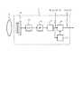
図1は、本実施形態の電子カメラの概略構成を示す図である。
電子カメラは、例えば、電子カメラ本体1と撮影レンズ2とからなる。
電子カメラ本体1には、カラー撮像素子11、A/D変換器12、ホワイトバランス処理回路14、画素補間回路15、色変換回路16、色変換マトリクス決定回路13(信号処理手段に対応する。)などが備えられる。
【0020】
カラー撮像素子11上に、撮影レンズ2による被写体の像が形成される。カラー撮像素子11の出力信号は、不図示のアナログゲイン回路を介してA/D変換器12に入力され、ディジタル信号に変換される。ディジタル信号には、ホワイトバランス処理回路14においてホワイトバランス処理が施され、補間回路15において画素補間の処理が施され、色変換回路16において階調変換処理が施され、その後、不図示のメモリに格納される。
【0021】
図2は、本実施形態のカラー撮像素子11を説明する図である。
図2(a)は、カラー撮像素子11の各画素ブロックB及び各画素Pを説明する図、図2(b)は、カラー撮像素子11の構成例を示す図である。
図2(a)に示すように、カラー撮像素子11の撮像面には、画素ブロックBがアレイ状に配置される。
【0022】
各画素ブロックBには、赤色光を検出するR画素(第1画素に対応。)Prと、緑色光を検出するG1画素(第2画素に対応。)Pg1と、青色光を検出するB画素(第3画素に対応。)Pbと、緑色光と青色光との間の波長の光を検出するG2画素(第4画素に対応。)Pg2とが田の字状に並べて配置される。
G2画素Pg2の前記光に対する感度は、G1画素Pg1の緑色光に対する感度よりも低く抑えられている。
【0023】
なお、G1画素Pg1とG2画素Pg2とは、各画素ブロックB内で互いに非隣接関係(つまり、図示したように右上と左下との関係、又は左上と右下との関係)で配置されることが望ましい。
なぜなら、後述するように、本実施形態の電子カメラでは、G1画素Pg1の出力とG2画素Pg2の出力とは、異種の画素の出力として処理される場合と、同種の画素の出力として処理される場合との双方があるので、G1画素Pg1とG2画素Pg2とを撮像面上で市松状かつ交互に配置させることが望ましいからである。
【0024】
このようなカラー撮像素子11は、例えば、図2(b)に示すように、可視光像を撮像する撮像素子11a(以下、各画素の特性が互いに等しいモノクロ撮像素子とする。)を用意し、その撮像素子11aの入射側に、カラーフィルタアレイ11bを配置することで構成される。
カラーフィルタアレイ11bは、フィルタブロックをアレイ状に配置しており、各フィルタブロックには、入射する可視光を赤色光に制限するRフィルタ部と、入射する可視光を緑色に制限するG1フィルタ部と、入射する可視光を青色光に制限するBフィルタ部と、入射する可視光を前記緑色光と前記青色光との間の波長の光に制限するG2フィルタ部とが並べて配置される。
【0025】
このうち、G2フィルタ部の前記光の透過率は、G1フィルタ部の前記緑色光の透過率よりも低く抑えられている。
このカラーフィルタアレイ11bによれば、撮像素子11bのうちRフィルタ部に対向する画素を、赤色光を検出するR画素Prとして使用することができ、G1フィルタ部に対向する画素を、緑色光を検出するG1画素Pg1として使用することができ、Bフィルタ部に対向する画素を、青色光を検出するB画素Pbとして使用することができ、G2フィルタ部に対向する画素を、緑色光と青色光との間の波長の光を検出するG2画素Pg2として使用することができる。
【0026】
なお、G1画素Pg1とG2画素Pg2とを市松状に交互に配置するべく、G1フィルタ部とG2フィルタ部とは、各フィルタブロック内で互いに非隣接関係(つまり、右上と左下との関係、又は左上と右下との関係)で配置されることが望ましい。
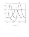
図3は、本実施形態のカラー撮像素子11の分光感度特性を示す図である。
【0027】
図3中、符号「R」で示す曲線がR画素Prの感度特性カーブに相当し、符号「G1」で示す曲線がG1画素Pg1の感度特性カーブに相当し、符号「B」で示す曲線がB画素Pbの感度特性カーブに相当し、符号「G2」で示す曲線がG2画素Pg2の感度特性カーブに相当する。
赤色光を検出するR画素Prの感度特性のピーク波長は、590nm〜640nmの範囲内にあり、緑色光を検出するG1画素Pg1の感度特性のピーク波長は、520nm〜570nmの範囲内にあり、青色光を検出するB画素Pbの感度特性のピーク波長は、430nm〜480nmの範囲内にある。
【0028】
また、青色光と緑色光との間の色を検出するG2画素Pg2の感度特性のピーク波長は、490nm〜530nmの範囲内にある。
例えば、R画素Prの感度特性のピーク波長は、600nmであり、G1画素Pg1の感度特性のピーク波長は、540nmであり、B画素Pbの感度特性のピーク波長は、460nmであり、G2画素Pg2の感度特性のピーク波長は、500nmである。
【0029】
因みに、カラー撮像素子11に対しこのような分光感度特性を付与するためのカラーフィルタアレイ11bの分光透過特性は、次のとおりである。
カラーフィルタアレイ11bのRフィルタ部の透過特性のピーク波長は、590nm〜640nmの範囲内にあり、G1フィルタ部の感度特性のピーク波長は、520nm〜570nmの範囲内にあり、Bフィルタ部の感度特性のピーク波長は、430nm〜480nmの範囲内にある。
【0030】
また、G2フィルタ部の感度特性のピーク波長は、490nm〜530nmの範囲内にある。
例えば、Rフィルタ部の透過特性のピーク波長は、600nmであり、G1フィルタ部の透過特性のピーク波長は、540nmであり、Bフィルタ部の透過特性のピーク波長は、460nmであり、G2フィルタ部の透過特性のピーク波長は、500nmである。
【0031】
図4は、等色関数(公知)を示す図である。
符号「r」,「g」,「b」で示すのがそれぞれ、RGB表色系の等色関数r,g,bである。
図3と図4とを比較すれば明らかなように、本実施形態のR画素の感度特性、G1画素の感度特性、B画素の感度特性は、それぞれ等色関数r、等色関数g、等色関数bに対応している。
【0032】
但し、等色関数rは、正のピークだけでなく、負のピークも有する。
本実施形態のG2画素の感度特性は、その等色関数rの負のピークに対応する位置にピークを有している。
よって、R画素の出力値、G1画素の出力値、B画素の出力値、及び、G2画素の出力値の反対符号に基づけば、等色関数r,g,bが表す色範囲(すなわち、人間の眼の検知可能な色範囲)とほぼ同じ色範囲において、色検出をすることができる。
【0033】
また、図3に明らかなように、G2画素の感度は、G1画素の感度よりも積極的に低く設定されている。例えば、G2画素の感度は、G1画素の感度の1/2程度であることが好ましい。
このように設定すれば、G2画素の飽和レベル(検出可能な輝度の上限を示す値)は、G1画素の飽和レベル(検出可能な輝度の上限を示す値)よりも高くなり、約2倍に設定される。
【0034】
さて、図1に示す画素補間回路15は、R画素Prの出力信号R,G1画素Pg1の出力信号G1、B画素Pbの出力信号B、G2画素Pg2の出力信号G2(なお、これらはA/D変換、ホワイトバランス処理後の出力信号である。)に基づいて画素補間を行い、各画素に入射した光の各色成分を示す信号(画素信号)(R,G1,G2,B)を生成する。
【0035】
なお、或る画素ブロックB内のR画素についての画素信号のG1成分,G2成分,B成分は、それぞれ周囲の画素ブロック内のG1画素,G2画素,B画素の各出力信号に基づいて得られる。
同様に、或る画素ブロックB内のG1画素についての画素信号のR成分,G2成分,B成分は、それぞれ周囲の画素ブロック内のR画素,G2画素,B画素の各出力信号に基づいて得られる。
【0036】
同様に、或る画素ブロックB内のG2画素についての画素信号のR成分,G1成分,B成分は、それぞれ周囲の画素ブロック内のR画素,G1画素,B画素の各出力信号に基づいて得られる。
同様に、或る画素ブロックB内のB画素についての画素信号のR成分,G1成分,G2成分は、それぞれ周囲の画素ブロック内のR画素,G1画素,G2画素の各出力信号に基づいて得られる。
【0037】
次に、色変換回路16は、式(1)のように画素信号(R,G1,G2,B)に対し3×4の色変換マトリクスMを乗算することで色変換を施し、表示用の色信号(R,G,B)を生成する。
【数1】
【0038】
色変換マトリクス決定回路13は、選択に当たり、画素信号(R,G1,G2,B)のG1成分を参照し、そのG1成分の値に応じた選択を行う。また、色変換マトリクス決定回路13は、選択の結果、必要がある場合には、ホワイトバランス再処理を行う(詳細は後述)。
マトリクスA,B,Cは、例えば、式(2)(3)(4)で表される。
【数2】
【0039】
ここで、図3に示したように、G1画素の感度特性とG2画素の感度特性とのピークは近接している。よって、G1成分とG2成分とは、微妙な色の相違を正確に表す。
したがって、マトリクスA又はマトリクスBは、画素信号(R,G1,G2,B)の微妙な色の相違を、色信号(R,G,B)に対し正確に反映するものである。
【0040】
なお、マトリクスA又はマトリクスBにおいて、1行3列成分(G2の係数)の符号は、何れも負となっているので、画素信号(R,G1,G2,B)のG2成分が大きいほど、色信号(R,G,B)のR成分は相対的に小さくなる。これにより、色信号(R,G,B)に対し、等色関数r,g,b(図3参照、青色と緑色との間に負のピークを有している。)による色再現と似た色再現をさせることが可能となっている。
【0041】
一方、式(4)を参照すれば明らかなように、マトリクスCは、画素信号(R,G1,G2,B)のG1成分に代えてG2成分を緑色を示す信号とみなし、R成分、G2成分、B成分を色信号(R,G,B)に反映させるものである。
ここで、上述したように、G1画素の感度特性とG2画素の感度特性とのピークは近接しており、また、G2画素の飽和レベルはG1画素の飽和レベルよりも高い(2倍高い)。よって、G2成分は、G1成分が示す色(緑色)の近接色の輝度を、G1成分よりも高いレベルまで正確に表す。
【0042】
したがって、マトリクスCは、画素信号(R,G1,G2,B)の高いレベルの輝度を、色信号(R,G,B)に対し正確に反映するものである。
図5は、色変換マトリクス決定回路13による処理の手順を説明する図である。
【0043】
色変換マトリクス決定回路13は、画素信号(R,G1,G2,B)のG1成分を参照する。
そして、G1成分の値が飽和レベル(G1画素の出力信号の飽和レベルに相当する値、例えば、3500)を超えていないとき(ステップS11YES又はNOかつステップS12YES)には、微妙な色の相違を正確に反映させるマトリクスA又はマトリクスBを選択し(ステップS21又はステップS22)、G1成分の値が飽和レベル(例えば、3500)を超えているとき(ステップS11NOかつステップS12NO)には、高いレベルの輝度を正確に反映するマトリクスCを選択する(ステップS23)。
【0044】
すなわち、本実施形態では、画素信号(R,G1,G2,B)のG1成分がG1画素の飽和レベルを超えていないとき(ステップS11YES、又はステップS11NOかつステップS12YES)には、検出色範囲が広がり、画素信号(R,G1,G2,B)のG1成分の値がG1画素の飽和レベルを超えているとき(ステップS11NOかつステップS12NO)には、検出色範囲は広がらないものの、高い輝度を正確に検出することができる。したがって、検出色範囲が拡大されつつも検出輝度範囲の縮小化は抑えられる。
【0045】
なお、式(2)(3)に示すように、マトリクスBとマトリクスAとを比較すると、第二列の係数(G1の係数)及び第三列の係数(G2の係数)の絶対値は、マトリクスBの方がマトリクスAよりも全体的に小さい(マトリクスBは、マトリクスAよりも、G1成分の反映量が小さく、また、G2成分の負の反映量が小さい。)。
【0046】
すなわち、マトリクスBは、マトリクスAとマトリクスC(G1成分の反映量が0であり、G2成分の反映量が大きい。)の中間の色変換を施すマトリクスである。
【0047】
よって、図5に示したように、G1成分の値が飽和レベルよりも小さい閾値(例えば3000)よりも低いときには(ステップS11YES)マトリクスAが選択され(ステップS21)、その閾値よりも高く飽和レベルよりも低いときには(ステップS11NOかつステップS11YES)マトリクスBを選択されることが好ましい(ステップS22)。
【0048】
このように、マトリクスCとマトリクスAだけでなく、両者の中間のマトリクスBを含めた3種類を使い分ければ、色変換がG1成分の相違に応じて急激に変化することが防止でき、再現画像上に不自然な表現が現れることが避けられる。
なお、ホワイトバランス処理回路14(図1参照)が各信号に対し乗算するホワイトバランスゲインは、マトリクスAを使用する場合の最適値になっているとする。
【0049】
このとき、マトリクスBが使用される場合、及びマトリクスCが使用される場合には、ステップS22、ステップS23の実行前に、ホワイトバランス再処理が施されることが好ましい(ステップS32、S33)。
なお、ステップS32のホワイトバランス再処理にて乗算すべきホワイトバランスゲインは、マトリクスAに代えてマトリクスBを使用する場合の最適値であり、ステップS33のホワイトバランス再処理にて乗算すべきホワイトバランスゲインは、マトリクスAに代えてマトリクスCを使用する場合の最適値である。
【0050】
[その他]
なお、上記実施形態では、G2画素の感度がG1画素の感度の「1/2」であるとしたが、1/2よりも若干大きく設定すれば、「検出色範囲の拡大」を「検出輝度範囲の縮小化を抑えること」よりも重視した処理にすることができ、1/2よりも若干小さく設定すれば、「検出輝度範囲の縮小化を抑えること」を「検出色範囲の拡大」よりも重視した処理にすることができる。G2感度とG1感度との関係は、両者のバランスを考慮して設定されることが好ましい。
【0051】
また、上記実施形態では、G2画素の検出色を、青色と緑色との間の色としたが、緑色と赤色との間の色に変更しても、その感度をG1画素よりも小さく(好ましくは約1/2に)設定すれば、上記実施形態と同様の効果を得ることができる。但し、色変換マトリクスの内容(行列要素の値)は、G2画素の感度特性に応じて適当なものに変更される。
【0052】
また、上記実施形態では、カラー撮像素子として、カラーフィルタアレイとモノクロ撮像素子とを組み合わせたものを例示したが、カラーフィルタを使用していないカラー撮像素子を使用することもできる。また、従来のカラー撮像素子(ベイヤ配列のカラー撮像素子など)に、新たなカラーフィルタアレイを重ねることによっても、上記実施形態のカラー撮像素子と同様の分光感度特性を付与することができる。
【0053】
【発明の効果】
以上、本発明によれば、検出色範囲を拡大しつつも検出輝度範囲の縮小化を抑えることが可能な単板式のカラー撮像素子が実現する。
また、本発明によれば、単板式のカラー撮像素子を構成するに当たり、検出色範囲を拡大しつつも検出輝度範囲の縮小化を抑えることが可能なカラーフィルタアレイが実現する。
【0054】
また、本発明によれば、検出色範囲を拡大しつつも検出輝度範囲の縮小化が抑えられたカラー撮像装置が実現する。
【図面の簡単な説明】
【図1】本実施形態の電子カメラの概略構成を示す図である。
【図2】本実施形態のカラー撮像素子11を説明する図である。
【図3】本実施形態のカラー撮像素子11の分光感度特性を示す図である。
【図4】等色関数(公知)を示す図である。
【図5】色変換マトリクス決定回路13による処理の手順を説明する図である。
【符号の説明】
1 電子カメラ本体
2 撮影レンズ
11 カラー撮像素子
12 A/D変換器
14 ホワイトバランス処理回路14
15 画素補間回路
16 色変換回路
13 色変換マトリクス決定回路
11b カラーフィルタアレイ
11a 撮像素子[0001]
The present invention relates an electronic camera,a color image pickup apparatus such as a video camera.
[0002]
[Prior art]
Conventionally, a color imaging device is applied to a color imaging device such as an electronic camera or a video camera.
In general, in a color imaging apparatus, it is desirable to make the spectral sensitivity characteristic of an imaging optical system from a photographing lens to a color imaging element as close as possible to the spectral sensitivity characteristic of human eyes (or a known color matching function).
[0003]
In the color imaging device, G pixels that detect green light, B pixels that detect blue light, and R pixels that detect red light are arranged in an array.
In particular, in the Bayer array, G pixels are arranged in a checkered pattern, and B pixels and R pixels are alternately arranged in a gap between the G pixels. That is, one unit (pixel block) is four pixels including two G pixels, one B pixel, and one R pixel.
[0004]
Incidentally, the reason why the number of G pixels is larger than that of R pixels and B pixels is as follows.
One characteristic of the human eye is that the number of cells that detect green is greater than the number of cells that detect other colors. Therefore, the human eye has a wide range in which the brightness of green light can be detected. Therefore, if a large number of G pixels are provided in the image sensor, the detection luminance range (a so-called dynamic range) can be expanded in the same manner as the human eye.
[0005]
By the way, the color range that can be discriminated by the three types of pixels of the R pixel, G pixel, and B pixel is slightly narrower than the color range that can be discriminated by the human eye. The colors may be detected as the same color.
For this reason, in recent years, a multiband color image pickup device in which another type of pixel is added has been proposed (for example, a color image pickup device described in Patent Document 1).
[0006]
The multiband color image sensor described in Patent Document 1 adds a Y pixel that detects a color (yellow) between green and red in addition to an R pixel, a G pixel, and a B pixel. The detection color range is expanded.
[Patent Document 1]
Japanese Patent Laid-Open No. 2002-271804
[Problems to be solved by the invention]
However, in this conventional multiband color image sensor, in order to add Y pixels in the pixel block, the two G pixels must be reduced to one. Therefore, the detection luminance range of green light tends to be reduced, and the detection luminance range of the color image sensor tends to be reduced.
[0008]
If the color image pickup device is a multi-plate type, Y pixels can be added without reducing the G pixels, so this problem does not occur. However, the optical path is branched and an image pickup device is arranged in each branch path. Therefore, it is not suitable for an electronic camera or a video camera that has a large layout space and is required to be downsized.
In addition, if a rotation type switching filter is applied, Y pixels can be added without reducing the G pixels, so this problem does not occur, but the arrangement space is expanded as in the case of a multi-plate type. It is not very suitable for electronic cameras and video cameras that require miniaturization.
[0010]
Another object of the present invention is to provide a color imaging apparatus in which the detection luminance range is reduced while the reduction of the detection luminance range is suppressed.
[0011]
The color imagingdevice according to claim 1, wherein the first pixel that detects red light, the second pixel that detects green light, the third pixel that detects blue light, the green light, and the blue light A pixel block consisting of a fourth pixel that detects light having a wavelength between the green light and the red light is arranged in an array, and the sensitivity of the fourth pixel to the light is determined by the second pixel. Acolor imaging device that is suppressed to be lower than the sensitivity to the green light,and a signal processing unit that generates a color signal based on each output of the first pixel, the second pixel, and the third pixel, When the output of the second pixel does not reach the saturation level, the signal processing means generates the color signal based on the output of the fourth pixel in addition to the respective outputs, and outputs the second pixel When the saturation level is reached, the output of the second pixel And generating said color signal based on the output of the fourth pixel, instead of based on.
[0012]
The color imagingdevice according to
[0013]
Color imagingapparatus according to
[0014]
According to a fourth aspect of the present invention, there is provided a colorimaging apparatus including a first filter unit that limits incident visible light to red light, a second filter unit that limits incident visible light to green, and incident visible light to blue light. A filter block comprising a third filter unit for limiting and a fourth filter unit for limiting incident visible light to light having a wavelength between the green light and the blue light or between the green light and the red light. Are arranged in anarray, and a color filter array in which the transmittance of the light of the fourth filter unit is suppressed to be lower than the transmittance of the green light of the second filter unit,and a pixel that detects visible light And the first pixel, the second pixel, and the third pixel facing the first filter unit, the second filter unit, and the third filter unit, respectively, of the pixels of the image sensor. Each output based on color Signal processing means for generating a signal, and when the output of the second pixel has not reached a saturation level, the signal processing means is based on the output of the fourth pixel in addition to the respective outputs. When a color signal is generated and the output of the second pixel reaches a saturation level, the color signal is generated based on the output of the fourth pixel instead of based on the output of the second pixel. Features.
[0015]
Colorimaging apparatus according to a fifth aspect, in the colorimaging device according to Claim 4, wherein the transmittance of the fourth filter portion is reduced to about 1/2 of the transmission rate of the second filter portion It is characterized by.
The colorimaging device according to claim 6, in the colorimaging device of claim 4 or claim 5, the peak wavelength in the visible light range of the transmission characteristic of the first filter unit is in the range of 590nm~640nm The peak wavelength in the visible light region of the transmission characteristic of the second filter portion is in the range of 520 nm to 570 nm, and the peak wavelength in the visible light region of the transmission property of the third filter portion is 430 nm to The peak wavelength in the visible light region of the transmission characteristic of the fourth filter portion is in the range of 480 nm to 530 nm, or in the range of 560 nm to 640 nm.
[0018]
DETAILED DESCRIPTION OF THE INVENTION
Hereinafter, embodiments of the present invention will be described with reference to the drawings.
[Embodiment]
This embodiment is an embodiment of an electronic camera (corresponding to the color imaging device of the present invention) to which the color imaging device of the present invention or the color filter array of the present invention is applied.
[0019]
FIG. 1 is a diagram showing a schematic configuration of the electronic camera of the present embodiment.
The electronic camera includes, for example, an electronic camera body 1 and a photographing
The electronic camera body 1 includes a
[0020]
An image of the subject is formed on the
[0021]
FIG. 2 is a diagram illustrating the
FIG. 2A is a diagram illustrating each pixel block B and each pixel P of the
As shown in FIG. 2A, pixel blocks B are arranged in an array on the imaging surface of the
[0022]
Each pixel block B includes an R pixel (corresponding to the first pixel) Pr that detects red light, a G1 pixel (corresponding to the second pixel) Pg1 that detects green light, and a B pixel that detects blue light. (Corresponding to the third pixel) Pb and a G2 pixel (corresponding to the fourth pixel) Pg2 for detecting light having a wavelength between green light and blue light are arranged in a square shape.
The sensitivity of the G2 pixel Pg2 to the light is suppressed to be lower than the sensitivity of the G1 pixel Pg1 to green light.
[0023]
Note that the G1 pixel Pg1 and the G2 pixel Pg2 are arranged in a non-adjacent relationship within each pixel block B (that is, the relationship between the upper right and the lower left, or the relationship between the upper left and the lower right as illustrated). Is desirable.
This is because, as will be described later, in the electronic camera of this embodiment, the output of the G1 pixel Pg1 and the output of the G2 pixel Pg2 are processed as outputs of different types of pixels and as outputs of the same kind of pixels. This is because it is desirable to arrange the G1 pixel Pg1 and the G2 pixel Pg2 in a checkered pattern and alternately on the imaging surface.
[0024]
As such a color
The
[0025]
Among these, the transmittance of the light of the G2 filter unit is suppressed to be lower than the transmittance of the green light of the G1 filter unit.
According to this
[0026]
In order to alternately arrange the G1 pixel Pg1 and the G2 pixel Pg2 in a checkered pattern, the G1 filter unit and the G2 filter unit are not adjacent to each other in each filter block (that is, the relationship between the upper right and the lower left, or It is desirable to arrange them in the relationship between the upper left and the lower right.
FIG. 3 is a diagram showing the spectral sensitivity characteristics of the
[0027]
In FIG. 3, the curve indicated by the symbol “R” corresponds to the sensitivity characteristic curve of the R pixel Pr, the curve indicated by the symbol “G1” corresponds to the sensitivity characteristic curve of the G1 pixel Pg1, and the curve indicated by the symbol “B”. The curve corresponding to the sensitivity characteristic curve of the B pixel Pb corresponds to the sensitivity characteristic curve of the G2 pixel Pg2.
The peak wavelength of the sensitivity characteristic of the R pixel Pr that detects red light is in the range of 590 nm to 640 nm, and the peak wavelength of the sensitivity characteristic of the G1 pixel Pg1 that detects green light is in the range of 520 nm to 570 nm. The peak wavelength of the sensitivity characteristic of the B pixel Pb that detects blue light is in the range of 430 nm to 480 nm.
[0028]
The peak wavelength of the sensitivity characteristic of the G2 pixel Pg2 that detects a color between blue light and green light is in the range of 490 nm to 530 nm.
For example, the peak wavelength of the sensitivity characteristic of the R pixel Pr is 600 nm, the peak wavelength of the sensitivity characteristic of the G1 pixel Pg1 is 540 nm, the peak wavelength of the sensitivity characteristic of the B pixel Pb is 460 nm, and the G2 pixel Pg2 The peak wavelength of the sensitivity characteristic is 500 nm.
[0029]
Incidentally, the spectral transmission characteristics of the
The peak wavelength of the transmission characteristic of the R filter part of the
[0030]
The peak wavelength of the sensitivity characteristic of the G2 filter portion is in the range of 490 nm to 530 nm.
For example, the peak wavelength of the transmission characteristic of the R filter unit is 600 nm, the peak wavelength of the transmission characteristic of the G1 filter unit is 540 nm, the peak wavelength of the transmission characteristic of the B filter unit is 460 nm, and the G2 filter unit The peak wavelength of the transmission characteristic is 500 nm.
[0031]
FIG. 4 is a diagram showing a color matching function (known).
Symbols “r”, “g”, and “b” indicate color matching functions r, g, and b of the RGB color system, respectively.
As is apparent from a comparison between FIG. 3 and FIG. 4, the sensitivity characteristics of the R pixel, the sensitivity characteristics of the G1 pixel, and the sensitivity characteristics of the B pixel of this embodiment are the color matching function r, the color matching function g, and the like, respectively. It corresponds to the color function b.
[0032]
However, the color matching function r has not only a positive peak but also a negative peak.
The sensitivity characteristic of the G2 pixel of this embodiment has a peak at a position corresponding to the negative peak of the color matching function r.
Therefore, based on the opposite sign of the output value of the R pixel, the output value of the G1 pixel, the output value of the B pixel, and the output value of the G2 pixel, the color range represented by the color matching functions r, g, b (that is, human Color detection can be performed in a color range that is substantially the same as the color range that can be detected by the eye.
[0033]
Further, as apparent from FIG. 3, the sensitivity of the G2 pixel is set to be lower than the sensitivity of the G1 pixel. For example, the sensitivity of the G2 pixel is preferably about ½ of the sensitivity of the G1 pixel.
With this setting, the saturation level of G2 pixel (a value indicating the upper limit of detectable luminance) becomes higher than the saturation level of G1 pixel (a value indicating the upper limit of detectable luminance), and is approximately doubled. Is set.
[0034]
The
[0035]
Note that the G1, G2, and B components of the pixel signal for an R pixel in a certain pixel block B are obtained based on the output signals of the G1, G2, and B pixels in the surrounding pixel blocks, respectively. .
Similarly, the R component, the G2 component, and the B component of the pixel signal for the G1 pixel in a certain pixel block B are obtained based on the output signals of the R pixel, the G2 pixel, and the B pixel in the surrounding pixel block, respectively. It is done.
[0036]
Similarly, the R component, G1 component, and B component of the pixel signal for the G2 pixel in a certain pixel block B are obtained based on the output signals of the R pixel, G1 pixel, and B pixel in the surrounding pixel block, respectively. It is done.
Similarly, the R component, G1 component, and G2 component of the pixel signal for the B pixel in a certain pixel block B are obtained based on the output signals of the R pixel, G1 pixel, and G2 pixel in the surrounding pixel block, respectively. It is done.
[0037]
Next, the
[Expression 1]
[0038]
In the selection, the color conversion
The matrices A, B, and C are expressed by, for example, formulas (2), (3), and (4).
[Expression 2]
[0039]
Here, as shown in FIG. 3, the peaks of the sensitivity characteristic of the G1 pixel and the sensitivity characteristic of the G2 pixel are close to each other. Therefore, the G1 component and the G2 component accurately represent subtle color differences.
Therefore, the matrix A or the matrix B accurately reflects the subtle color difference of the pixel signals (R, G1, G2, B) on the color signals (R, G, B).
[0040]
In addition, in the matrix A or the matrix B, since the sign of the 1
[0041]
On the other hand, as apparent from reference to Expression (4), the matrix C regards the G2 component as a signal indicating green instead of the G1 component of the pixel signal (R, G1, G2, B), and the R component, G2 The component and the B component are reflected in the color signal (R, G, B).
Here, as described above, the peak of the sensitivity characteristic of the G1 pixel and the sensitivity characteristic of the G2 pixel are close to each other, and the saturation level of the G2 pixel is higher (two times higher) than the saturation level of the G1 pixel. Therefore, the G2 component accurately represents the brightness of the adjacent color of the color (green) indicated by the G1 component to a level higher than that of the G1 component.
[0042]
Therefore, the matrix C accurately reflects the high level luminance of the pixel signals (R, G1, G2, B) on the color signals (R, G, B).
FIG. 5 is a diagram for explaining the procedure of processing performed by the color conversion
[0043]
The color conversion
When the value of the G1 component does not exceed the saturation level (a value corresponding to the saturation level of the output signal of the G1 pixel, for example, 3500) (step S11YES or NO and step S12YES), a subtle color difference is obtained. When matrix A or matrix B to be accurately reflected is selected (step S21 or step S22) and the value of the G1 component exceeds a saturation level (eg, 3500) (step S11NO and step S12NO), a high level is selected. A matrix C that accurately reflects the luminance is selected (step S23).
[0044]
That is, in the present embodiment, when the G1 component of the pixel signal (R, G1, G2, B) does not exceed the saturation level of the G1 pixel (step S11YES, or step S11NO and step S12YES), the detected color range is When the value of the G1 component of the pixel signal (R, G1, G2, B) exceeds the saturation level of the G1 pixel (step S11NO and step S12NO), the detected color range does not widen, but high brightness is obtained. It can be detected accurately. Therefore, the detection luminance range can be prevented from being reduced while the detection color range is expanded.
[0045]
As shown in equations (2) and (3), when the matrix B and the matrix A are compared, the absolute values of the second column coefficient (G1 coefficient) and the third column coefficient (G2 coefficient) are: The matrix B is generally smaller than the matrix A (the matrix B has a smaller reflection amount of the G1 component and a smaller negative reflection amount of the G2 component than the matrix A).
[0046]
That is, the matrix B is a matrix that performs intermediate color conversion between the matrix A and the matrix C (the reflection amount of the G1 component is 0 and the reflection amount of the G2 component is large).
[0047]
Therefore, as shown in FIG. 5, when the value of the G1 component is lower than a threshold value (eg, 3000) smaller than the saturation level (step S11 YES), the matrix A is selected (step S21), and the saturation level is higher than the threshold value. Is lower (step S11NO and step S11YES), the matrix B is preferably selected (step S22).
[0048]
In this way, by using not only the matrix C and the matrix A but also the three types including the matrix B between them, the color conversion can be prevented from changing rapidly according to the difference in the G1 component, and the reproduced image can be prevented. An unnatural expression on the top can be avoided.
It is assumed that the white balance gain multiplied by each signal by the white balance processing circuit 14 (see FIG. 1) is an optimum value when the matrix A is used.
[0049]
At this time, when the matrix B is used and when the matrix C is used, it is preferable that white balance reprocessing is performed before the execution of steps S22 and S23 (steps S32 and S33).
Note that the white balance gain to be multiplied in the white balance reprocessing in step S32 is an optimum value when the matrix B is used instead of the matrix A, and the white balance to be multiplied in the white balance reprocessing in step S33. The gain is an optimum value when the matrix C is used instead of the matrix A.
[0050]
[Others]
In the above embodiment, the sensitivity of the G2 pixel is “1/2” of the sensitivity of the G1 pixel. However, if the sensitivity is set to be slightly larger than 1/2, “expansion of the detection color range” is set to “detection luminance”. It is possible to make processing more important than “suppressing the reduction of the range”, and if it is set slightly smaller than ½, “suppressing the reduction of the detection luminance range” is referred to as “expansion of the detection color range”. Can also be treated with emphasis. The relationship between the G2 sensitivity and the G1 sensitivity is preferably set in consideration of the balance between the two.
[0051]
In the above embodiment, the detection color of the G2 pixel is set to a color between blue and green. However, even if it is changed to a color between green and red, the sensitivity is smaller than that of the G1 pixel (preferably Is set to about ½), the same effect as in the above embodiment can be obtained. However, the content of the color conversion matrix (the value of the matrix element) is changed to an appropriate one according to the sensitivity characteristic of the G2 pixel.
[0052]
In the above embodiment, a combination of a color filter array and a monochrome image pickup device is exemplified as the color image pickup device. However, a color image pickup device that does not use a color filter can also be used. Further, the same spectral sensitivity characteristic as that of the color image sensor of the above-described embodiment can be imparted by superimposing a new color filter array on a conventional color image sensor (such as a Bayer array color image sensor).
[0053]
【The invention's effect】
As described above, according to the present invention, it is possible to realize a single-plate type color imaging device capable of suppressing the reduction of the detection luminance range while expanding the detection color range.
In addition, according to the present invention, a color filter array capable of suppressing the reduction of the detection luminance range while expanding the detection color range when configuring a single-plate color image sensor is realized.
[0054]
In addition, according to the present invention, a color imaging device is realized in which the detection color range is enlarged while the reduction of the detection luminance range is suppressed.
[Brief description of the drawings]
FIG. 1 is a diagram illustrating a schematic configuration of an electronic camera according to an embodiment.
FIG. 2 is a diagram illustrating a
FIG. 3 is a diagram showing spectral sensitivity characteristics of the
FIG. 4 is a diagram illustrating a color matching function (known).
FIG. 5 is a diagram illustrating a processing procedure performed by a color conversion
[Explanation of symbols]
1
15
Claims (6)
Translated fromJapanese緑色光を検出する第2画素と、
青色光を検出する第3画素と、
前記緑色光と前記青色光との間又は前記緑色光と前記赤色光との間の波長の光を検出する第4画素と
からなる画素ブロックをアレイ状に配置し、
前記第4画素の前記光に対する感度は、前記第2画素の前記緑色光に対する感度よりも低く抑えられているカラー撮像素子と、
前記第1画素、前記第2画素、前記第3画素の各出力に基づいて色信号を生成する信号処理手段とを備え、
前記信号処理手段は、
前記第2画素の出力が飽和レベルに達していない場合には、前記各出力に加えて前記第4画素の出力に基づいて前記色信号を生成し、前記第2画素の出力が飽和レベルに達している場合には、その第2画素の出力に基づく代わりに前記第4画素の出力に基づいて前記色信号を生成する
ことを特徴とするカラー撮像装置。A first pixel for detecting red light;
A second pixel for detecting green light;
A third pixel for detecting blue light;
A pixel block composed of a fourth pixel that detects light having a wavelength between the green light and the blue light or between the green light and the red light is arranged in an array,
A color imaging device inwhich the sensitivity of the fourth pixel to the light is suppressed to be lower than the sensitivity of the second pixel to the green light;
Signal processing means for generating a color signal based on each output of the first pixel, the second pixel, and the third pixel;
The signal processing means includes
When the output of the second pixel does not reach the saturation level, the color signal is generated based on the output of the fourth pixel in addition to the respective outputs, and the output of the second pixel reaches the saturation level. If so, the color signal is generated based on the output of the fourth pixel instead of based on the output of the second pixel.
A color imaging apparatus characterized by the above.
前記第4画素の前記感度は、前記第2画素の前記感度の略1/2に抑えられている
ことを特徴とするカラー撮像装置。The color imagingdevice according to claim 1,
The color imagingdevice , wherein the sensitivity of the fourth pixel is suppressed to approximately ½ of the sensitivity of the second pixel.
前記第1画素の感度特性のピーク波長は、590nm〜640nmの範囲内にあり、
前記第2画素の感度特性のピーク波長は、520nm〜570nmの範囲内にあり、
前記第3画素の感度特性のピーク波長は、430nm〜480nmの範囲内にあり、
前記第4画素の感度特性のピーク波長は、490nm〜530nmの範囲内、又は560nm〜640nmの範囲内にある
ことを特徴とするカラー撮像装置。In the color imagingdevice according to claim 1 or 2,
The peak wavelength of the sensitivity characteristic of the first pixel is in the range of 590 nm to 640 nm,
The peak wavelength of the sensitivity characteristic of the second pixel is in the range of 520 nm to 570 nm,
The peak wavelength of the sensitivity characteristic of the third pixel is in the range of 430 nm to 480 nm,
The color imagingdevice, wherein the peak wavelength of the sensitivity characteristic of the fourth pixel is in the range of 490 nm to 530 nm or in the range of 560 nm to 640 nm.
入射する可視光を緑色に制限する第2フィルタ部と、
入射する可視光を青色光に制限する第3フィルタ部と、
入射する可視光を前記緑色光と前記青色光との間又は前記緑色光と前記赤色光との間の波長の光に制限する第4フィルタ部と
からなるフィルタブロックをアレイ状に配置し、
前記第4フィルタ部の前記光の透過率は、前記第2フィルタ部の前記緑色光の透過率よりも低く抑えられているカラーフィルタアレイと、
可視光を検出する画素をアレイ状に配置した撮像素子と、
前記撮像素子の前記画素のうち前記第1フィルタ部、前記第2フィルタ部、前記第3フィルタ部にそれぞれ対向する第1画素、第2画素、第3画素の各出力に基づいて色信号を生成する信号処理手段とを備え、
前記信号処理手段は、
前記第2画素の出力が飽和レベルに達していない場合には、前記各出力に加えて前記第4画素の出力に基づいて前記色信号を生成し、前記第2画素の出力が飽和レベルに達している場合には、その第2画素の出力に基づく代わりに前記第4画素の出力に基づいて前記色信号を生成する
ことを特徴とするカラー撮像装置。A first filter unit for limiting incident visible light to red light;
A second filter unit that limits incident visible light to green;
A third filter unit for limiting incident visible light to blue light;
A filter block comprising: a fourth filter unit that limits incident visible light to light having a wavelength between the green light and the blue light or between the green light and the red light; and arranged in an array.
A color filter array inwhich the light transmittance of the fourth filter portion is suppressed to be lower than the transmittance of the green light of the second filter portion;
An image sensor in which pixels for detecting visible light are arranged in an array;
A color signal is generated based on outputs of the first pixel, the second pixel, and the third pixel facing the first filter unit, the second filter unit, and the third filter unit, respectively, of the pixels of the image sensor. Signal processing means for
The signal processing means includes
When the output of the second pixel does not reach the saturation level, the color signal is generated based on the output of the fourth pixel in addition to the respective outputs, and the output of the second pixel reaches the saturation level. If so, the color signal is generated based on the output of the fourth pixel instead of based on the output of the second pixel.
A color imaging apparatus characterized by the above.
前記第4フィルタ部の前記透過率は、前記第2フィルタ部の前記透過率の略1/2に抑えられている
ことを特徴とするカラー撮像装置。The colorimaging device according to claim 4,
The colorimaging apparatus , wherein the transmittance of the fourth filter unit is suppressed to approximately ½ of the transmittance of the second filter unit.
前記第1フィルタ部の透過特性の可視光領域でのピーク波長は、590nm〜640nmの範囲内にあり、
前記第2フィルタ部の透過特性の可視光領域でのピーク波長は、520nm〜570nmの範囲内にあり、
前記第3フィルタ部の透過特性の可視光領域でのピーク波長は、430nm〜480nmの範囲内にあり、
前記第4フィルタ部の透過特性の可視光領域でのピーク波長は、490nm〜530nmの範囲内、又は560nm〜640nmの範囲内にある
ことを特徴とするカラー撮像装置。In the colorimaging device according to claim 4 or 5,
The peak wavelength in the visible light region of the transmission characteristics of the first filter portion is in the range of 590 nm to 640 nm,
The peak wavelength in the visible light region of the transmission characteristics of the second filter portion is in the range of 520 nm to 570 nm,
The peak wavelength in the visible light region of the transmission characteristics of the third filter portion is in the range of 430 nm to 480 nm,
The colorimaging device , wherein a peak wavelength in a visible light region of transmission characteristics of the fourth filter unit is in a range of 490 nm to 530 nm or in a range of 560 nm to 640 nm.
Priority Applications (7)
| Application Number | Priority Date | Filing Date | Title |
|---|---|---|---|
| JP2002366296AJP4465958B2 (en) | 2002-12-18 | 2002-12-18 | Color imaging device |
| EP03778803AEP1575304B1 (en) | 2002-12-18 | 2003-12-11 | Color imaging element, color filter array, and color imaging device |
| PCT/JP2003/015859WO2004056127A1 (en) | 2002-12-18 | 2003-12-11 | Color imaging element, color filter array, and color imaging device |
| AU2003289025AAU2003289025A1 (en) | 2002-12-18 | 2003-12-11 | Color imaging element, color filter array, and color imaging device |
| AT03778803TATE546016T1 (en) | 2002-12-18 | 2003-12-11 | COLOR IMAGING ELEMENT, COLOR FILTER GROUP AND COLOR IMAGING DEVICE |
| CNB2003801069748ACN100481959C (en) | 2002-12-18 | 2003-12-11 | Color image sensor, color filter array and color imaging apparatus |
| US11/137,322US7633537B2 (en) | 2002-12-18 | 2005-05-26 | Color image sensor, color filter array and color imaging device |
Applications Claiming Priority (1)
| Application Number | Priority Date | Filing Date | Title |
|---|---|---|---|
| JP2002366296AJP4465958B2 (en) | 2002-12-18 | 2002-12-18 | Color imaging device |
Publications (2)
| Publication Number | Publication Date |
|---|---|
| JP2004200357A JP2004200357A (en) | 2004-07-15 |
| JP4465958B2true JP4465958B2 (en) | 2010-05-26 |
Family
ID=32588302
Family Applications (1)
| Application Number | Title | Priority Date | Filing Date |
|---|---|---|---|
| JP2002366296AExpired - Fee RelatedJP4465958B2 (en) | 2002-12-18 | 2002-12-18 | Color imaging device |
Country Status (6)
| Country | Link |
|---|---|
| EP (1) | EP1575304B1 (en) |
| JP (1) | JP4465958B2 (en) |
| CN (1) | CN100481959C (en) |
| AT (1) | ATE546016T1 (en) |
| AU (1) | AU2003289025A1 (en) |
| WO (1) | WO2004056127A1 (en) |
Families Citing this family (14)
| Publication number | Priority date | Publication date | Assignee | Title |
|---|---|---|---|---|
| JP4118916B2 (en) | 2003-11-11 | 2008-07-16 | オリンパス株式会社 | Multispectral imaging device |
| US7864235B2 (en) | 2005-03-30 | 2011-01-04 | Hoya Corporation | Imaging device and imaging method including generation of primary color signals |
| JP4859502B2 (en)* | 2005-03-30 | 2012-01-25 | Hoya株式会社 | Imaging device |
| JP4533261B2 (en)* | 2005-06-30 | 2010-09-01 | 日本放送協会 | Imaging device |
| JP2007086178A (en)* | 2005-09-20 | 2007-04-05 | Fujifilm Corp | Camera strobe device and imaging device |
| JP4874752B2 (en)* | 2006-09-27 | 2012-02-15 | Hoya株式会社 | Digital camera |
| JP2012513694A (en)* | 2008-12-22 | 2012-06-14 | コーニンクレッカ フィリップス エレクトロニクス エヌ ヴィ | CMOS imaging device with single photon counting function |
| JP5146499B2 (en) | 2009-08-08 | 2013-02-20 | 株式会社ニコン | Solid-state image sensor |
| CN103149733B (en)* | 2013-03-29 | 2016-02-24 | 京东方科技集团股份有限公司 | Color membrane substrates, display panel and display device |
| TWI781085B (en)* | 2015-11-24 | 2022-10-21 | 日商索尼半導體解決方案公司 | Fly-eye lens module and fly-eye camera module |
| GB201602272D0 (en)* | 2016-02-09 | 2016-03-23 | Univ Manchester | Improvements in image formation |
| WO2021155925A1 (en)* | 2020-02-06 | 2021-08-12 | Huawei Technologies Co., Ltd. | Color filter array and pipeline for image processing |
| CN111918004B (en)* | 2020-09-16 | 2023-07-04 | Oppo广东移动通信有限公司 | Image sensor, terminal, data processing method, device and storage medium |
| JP2024097101A (en)* | 2021-05-11 | 2024-07-18 | ソニーセミコンダクタソリューションズ株式会社 | Image pickup device, image pickup device and electronic device |
Family Cites Families (5)
| Publication number | Priority date | Publication date | Assignee | Title |
|---|---|---|---|---|
| JP2872759B2 (en)* | 1989-06-08 | 1999-03-24 | 富士写真フイルム株式会社 | Solid-state imaging system |
| JP3046701B2 (en)* | 1993-12-24 | 2000-05-29 | シャープ株式会社 | Color liquid crystal display |
| CN1288549A (en)* | 1998-09-15 | 2001-03-21 | 第一阶段公司 | Method and system for processing images |
| JP2001016598A (en)* | 1999-04-30 | 2001-01-19 | Olympus Optical Co Ltd | Color imaging device and image pickup device |
| US6924841B2 (en)* | 2001-05-02 | 2005-08-02 | Agilent Technologies, Inc. | System and method for capturing color images that extends the dynamic range of an image sensor using first and second groups of pixels |
- 2002
- 2002-12-18JPJP2002366296Apatent/JP4465958B2/ennot_activeExpired - Fee Related
- 2003
- 2003-12-11ATAT03778803Tpatent/ATE546016T1/enactive
- 2003-12-11AUAU2003289025Apatent/AU2003289025A1/ennot_activeAbandoned
- 2003-12-11EPEP03778803Apatent/EP1575304B1/ennot_activeExpired - Lifetime
- 2003-12-11WOPCT/JP2003/015859patent/WO2004056127A1/enactiveApplication Filing
- 2003-12-11CNCNB2003801069748Apatent/CN100481959C/ennot_activeExpired - Fee Related
Also Published As
| Publication number | Publication date |
|---|---|
| ATE546016T1 (en) | 2012-03-15 |
| AU2003289025A1 (en) | 2004-07-09 |
| JP2004200357A (en) | 2004-07-15 |
| CN1729697A (en) | 2006-02-01 |
| CN100481959C (en) | 2009-04-22 |
| EP1575304A1 (en) | 2005-09-14 |
| EP1575304B1 (en) | 2012-02-15 |
| WO2004056127A1 (en) | 2004-07-01 |
| EP1575304A4 (en) | 2006-05-24 |
Similar Documents
| Publication | Publication Date | Title |
|---|---|---|
| JP4453189B2 (en) | Imaging device | |
| US7400332B2 (en) | Hexagonal color pixel structure with white pixels | |
| US8805070B2 (en) | Image processing apparatus and image processing method | |
| KR100580911B1 (en) | Image synthesis method and image pickup apparatus | |
| US8508625B2 (en) | Image processing apparatus | |
| US20050248667A1 (en) | Extended dynamic range in color imagers | |
| JP4465958B2 (en) | Color imaging device | |
| US20070153099A1 (en) | Image signal processing apparatus, imaging apparatus, image signal processing method and computer program thereof | |
| US7880773B2 (en) | Imaging device | |
| US7633537B2 (en) | Color image sensor, color filter array and color imaging device | |
| US8086032B2 (en) | Image processing device, image processing method, and image pickup apparatus | |
| US7864235B2 (en) | Imaging device and imaging method including generation of primary color signals | |
| CN209345244U (en) | Imaging Systems and Camera Modules | |
| US7231085B2 (en) | Color image signal processing method for correcting hue turn and color image outputting device and imaging device | |
| US7046277B2 (en) | Image interpolating device, including interpolation and modification processors | |
| US6747698B2 (en) | Image interpolating device | |
| JP3490888B2 (en) | Color suppression circuit | |
| US6900833B2 (en) | Image interpolating device | |
| JP2013219452A (en) | Color signal processing circuit, color signal processing method, color reproduction evaluation method, imaging apparatus, electronic apparatus and testing apparatus | |
| JP2004222160A (en) | Digital camera | |
| US7512266B2 (en) | Method and device for luminance correction | |
| JPH08181909A (en) | Imaging device | |
| JPH11164309A (en) | Image signal processing method and electronic camera | |
| JP2005295419A (en) | Imaging apparatus, camera, and signal processing method | |
| JP2006148791A (en) | Imaging device |
Legal Events
| Date | Code | Title | Description |
|---|---|---|---|
| A621 | Written request for application examination | Free format text:JAPANESE INTERMEDIATE CODE: A621 Effective date:20051101 | |
| A131 | Notification of reasons for refusal | Free format text:JAPANESE INTERMEDIATE CODE: A131 Effective date:20090901 | |
| A521 | Request for written amendment filed | Free format text:JAPANESE INTERMEDIATE CODE: A523 Effective date:20091021 | |
| TRDD | Decision of grant or rejection written | ||
| A01 | Written decision to grant a patent or to grant a registration (utility model) | Free format text:JAPANESE INTERMEDIATE CODE: A01 Effective date:20100202 | |
| A01 | Written decision to grant a patent or to grant a registration (utility model) | Free format text:JAPANESE INTERMEDIATE CODE: A01 | |
| A61 | First payment of annual fees (during grant procedure) | Free format text:JAPANESE INTERMEDIATE CODE: A61 Effective date:20100215 | |
| R150 | Certificate of patent or registration of utility model | Ref document number:4465958 Country of ref document:JP Free format text:JAPANESE INTERMEDIATE CODE: R150 Free format text:JAPANESE INTERMEDIATE CODE: R150 | |
| FPAY | Renewal fee payment (event date is renewal date of database) | Free format text:PAYMENT UNTIL: 20130305 Year of fee payment:3 | |
| FPAY | Renewal fee payment (event date is renewal date of database) | Free format text:PAYMENT UNTIL: 20130305 Year of fee payment:3 | |
| S531 | Written request for registration of change of domicile | Free format text:JAPANESE INTERMEDIATE CODE: R313531 | |
| FPAY | Renewal fee payment (event date is renewal date of database) | Free format text:PAYMENT UNTIL: 20130305 Year of fee payment:3 | |
| R350 | Written notification of registration of transfer | Free format text:JAPANESE INTERMEDIATE CODE: R350 | |
| FPAY | Renewal fee payment (event date is renewal date of database) | Free format text:PAYMENT UNTIL: 20130305 Year of fee payment:3 | |
| FPAY | Renewal fee payment (event date is renewal date of database) | Free format text:PAYMENT UNTIL: 20130305 Year of fee payment:3 | |
| FPAY | Renewal fee payment (event date is renewal date of database) | Free format text:PAYMENT UNTIL: 20140305 Year of fee payment:4 | |
| R250 | Receipt of annual fees | Free format text:JAPANESE INTERMEDIATE CODE: R250 | |
| R250 | Receipt of annual fees | Free format text:JAPANESE INTERMEDIATE CODE: R250 | |
| R250 | Receipt of annual fees | Free format text:JAPANESE INTERMEDIATE CODE: R250 | |
| R250 | Receipt of annual fees | Free format text:JAPANESE INTERMEDIATE CODE: R250 | |
| R250 | Receipt of annual fees | Free format text:JAPANESE INTERMEDIATE CODE: R250 | |
| R250 | Receipt of annual fees | Free format text:JAPANESE INTERMEDIATE CODE: R250 | |
| R250 | Receipt of annual fees | Free format text:JAPANESE INTERMEDIATE CODE: R250 | |
| LAPS | Cancellation because of no payment of annual fees |