JP4464949B2 - Substrate processing apparatus and selective epitaxial film growth method - Google Patents
Substrate processing apparatus and selective epitaxial film growth methodDownload PDFInfo
- Publication number
- JP4464949B2 JP4464949B2JP2006304936AJP2006304936AJP4464949B2JP 4464949 B2JP4464949 B2JP 4464949B2JP 2006304936 AJP2006304936 AJP 2006304936AJP 2006304936 AJP2006304936 AJP 2006304936AJP 4464949 B2JP4464949 B2JP 4464949B2
- Authority
- JP
- Japan
- Prior art keywords
- gas
- gas supply
- processing chamber
- supplying
- substrate
- Prior art date
- Legal status (The legal status is an assumption and is not a legal conclusion. Google has not performed a legal analysis and makes no representation as to the accuracy of the status listed.)
- Active
Links
Images

Classifications
- C—CHEMISTRY; METALLURGY
- C23—COATING METALLIC MATERIAL; COATING MATERIAL WITH METALLIC MATERIAL; CHEMICAL SURFACE TREATMENT; DIFFUSION TREATMENT OF METALLIC MATERIAL; COATING BY VACUUM EVAPORATION, BY SPUTTERING, BY ION IMPLANTATION OR BY CHEMICAL VAPOUR DEPOSITION, IN GENERAL; INHIBITING CORROSION OF METALLIC MATERIAL OR INCRUSTATION IN GENERAL
- C23C—COATING METALLIC MATERIAL; COATING MATERIAL WITH METALLIC MATERIAL; SURFACE TREATMENT OF METALLIC MATERIAL BY DIFFUSION INTO THE SURFACE, BY CHEMICAL CONVERSION OR SUBSTITUTION; COATING BY VACUUM EVAPORATION, BY SPUTTERING, BY ION IMPLANTATION OR BY CHEMICAL VAPOUR DEPOSITION, IN GENERAL
- C23C16/00—Chemical coating by decomposition of gaseous compounds, without leaving reaction products of surface material in the coating, i.e. chemical vapour deposition [CVD] processes
- C23C16/22—Chemical coating by decomposition of gaseous compounds, without leaving reaction products of surface material in the coating, i.e. chemical vapour deposition [CVD] processes characterised by the deposition of inorganic material, other than metallic material
- C23C16/24—Deposition of silicon only
- C—CHEMISTRY; METALLURGY
- C23—COATING METALLIC MATERIAL; COATING MATERIAL WITH METALLIC MATERIAL; CHEMICAL SURFACE TREATMENT; DIFFUSION TREATMENT OF METALLIC MATERIAL; COATING BY VACUUM EVAPORATION, BY SPUTTERING, BY ION IMPLANTATION OR BY CHEMICAL VAPOUR DEPOSITION, IN GENERAL; INHIBITING CORROSION OF METALLIC MATERIAL OR INCRUSTATION IN GENERAL
- C23C—COATING METALLIC MATERIAL; COATING MATERIAL WITH METALLIC MATERIAL; SURFACE TREATMENT OF METALLIC MATERIAL BY DIFFUSION INTO THE SURFACE, BY CHEMICAL CONVERSION OR SUBSTITUTION; COATING BY VACUUM EVAPORATION, BY SPUTTERING, BY ION IMPLANTATION OR BY CHEMICAL VAPOUR DEPOSITION, IN GENERAL
- C23C16/00—Chemical coating by decomposition of gaseous compounds, without leaving reaction products of surface material in the coating, i.e. chemical vapour deposition [CVD] processes
- C23C16/22—Chemical coating by decomposition of gaseous compounds, without leaving reaction products of surface material in the coating, i.e. chemical vapour deposition [CVD] processes characterised by the deposition of inorganic material, other than metallic material
- C—CHEMISTRY; METALLURGY
- C30—CRYSTAL GROWTH
- C30B—SINGLE-CRYSTAL GROWTH; UNIDIRECTIONAL SOLIDIFICATION OF EUTECTIC MATERIAL OR UNIDIRECTIONAL DEMIXING OF EUTECTOID MATERIAL; REFINING BY ZONE-MELTING OF MATERIAL; PRODUCTION OF A HOMOGENEOUS POLYCRYSTALLINE MATERIAL WITH DEFINED STRUCTURE; SINGLE CRYSTALS OR HOMOGENEOUS POLYCRYSTALLINE MATERIAL WITH DEFINED STRUCTURE; AFTER-TREATMENT OF SINGLE CRYSTALS OR A HOMOGENEOUS POLYCRYSTALLINE MATERIAL WITH DEFINED STRUCTURE; APPARATUS THEREFOR
- C30B25/00—Single-crystal growth by chemical reaction of reactive gases, e.g. chemical vapour-deposition growth
- C30B25/02—Epitaxial-layer growth
- C30B25/08—Reaction chambers; Selection of materials therefor
- C—CHEMISTRY; METALLURGY
- C30—CRYSTAL GROWTH
- C30B—SINGLE-CRYSTAL GROWTH; UNIDIRECTIONAL SOLIDIFICATION OF EUTECTIC MATERIAL OR UNIDIRECTIONAL DEMIXING OF EUTECTOID MATERIAL; REFINING BY ZONE-MELTING OF MATERIAL; PRODUCTION OF A HOMOGENEOUS POLYCRYSTALLINE MATERIAL WITH DEFINED STRUCTURE; SINGLE CRYSTALS OR HOMOGENEOUS POLYCRYSTALLINE MATERIAL WITH DEFINED STRUCTURE; AFTER-TREATMENT OF SINGLE CRYSTALS OR A HOMOGENEOUS POLYCRYSTALLINE MATERIAL WITH DEFINED STRUCTURE; APPARATUS THEREFOR
- C30B25/00—Single-crystal growth by chemical reaction of reactive gases, e.g. chemical vapour-deposition growth
- C30B25/02—Epitaxial-layer growth
- C30B25/14—Feed and outlet means for the gases; Modifying the flow of the reactive gases
- C—CHEMISTRY; METALLURGY
- C30—CRYSTAL GROWTH
- C30B—SINGLE-CRYSTAL GROWTH; UNIDIRECTIONAL SOLIDIFICATION OF EUTECTIC MATERIAL OR UNIDIRECTIONAL DEMIXING OF EUTECTOID MATERIAL; REFINING BY ZONE-MELTING OF MATERIAL; PRODUCTION OF A HOMOGENEOUS POLYCRYSTALLINE MATERIAL WITH DEFINED STRUCTURE; SINGLE CRYSTALS OR HOMOGENEOUS POLYCRYSTALLINE MATERIAL WITH DEFINED STRUCTURE; AFTER-TREATMENT OF SINGLE CRYSTALS OR A HOMOGENEOUS POLYCRYSTALLINE MATERIAL WITH DEFINED STRUCTURE; APPARATUS THEREFOR
- C30B29/00—Single crystals or homogeneous polycrystalline material with defined structure characterised by the material or by their shape
- C30B29/02—Elements
- C30B29/06—Silicon
- C—CHEMISTRY; METALLURGY
- C30—CRYSTAL GROWTH
- C30B—SINGLE-CRYSTAL GROWTH; UNIDIRECTIONAL SOLIDIFICATION OF EUTECTIC MATERIAL OR UNIDIRECTIONAL DEMIXING OF EUTECTOID MATERIAL; REFINING BY ZONE-MELTING OF MATERIAL; PRODUCTION OF A HOMOGENEOUS POLYCRYSTALLINE MATERIAL WITH DEFINED STRUCTURE; SINGLE CRYSTALS OR HOMOGENEOUS POLYCRYSTALLINE MATERIAL WITH DEFINED STRUCTURE; AFTER-TREATMENT OF SINGLE CRYSTALS OR A HOMOGENEOUS POLYCRYSTALLINE MATERIAL WITH DEFINED STRUCTURE; APPARATUS THEREFOR
- C30B35/00—Apparatus not otherwise provided for, specially adapted for the growth, production or after-treatment of single crystals or of a homogeneous polycrystalline material with defined structure
Landscapes
- Chemical & Material Sciences (AREA)
- Engineering & Computer Science (AREA)
- Materials Engineering (AREA)
- Metallurgy (AREA)
- Organic Chemistry (AREA)
- General Chemical & Material Sciences (AREA)
- Chemical Kinetics & Catalysis (AREA)
- Crystallography & Structural Chemistry (AREA)
- Inorganic Chemistry (AREA)
- Mechanical Engineering (AREA)
- Chemical Vapour Deposition (AREA)
Description
Translated fromJapanese本発明は、半導体製造装置に用いる基板処理装置に関するものである。 The present invention relates to a substrate processing apparatus used in a semiconductor manufacturing apparatus.
従来のSi又はSiGeの選択エピタキシャル成長に用いられる縦型減圧CVD装置の反応炉(処理炉)は、反応管とインレットフランジ、シールキャップ等により構成され、シールキャップ上にボートが載せられ、そのボートにウェハが配置され、反応炉内がヒータにより加熱される。
この構成において、SiまたはSiGeの選択エピタキシャル成長の原料となるガスは、ノズルを通じて反応炉内上部から導入され、下部より排気される。よってウェハの存在する反応雰囲気でのガスの流れは上から下となる。
このとき、反応炉を加熱するヒータは上部ヒータ、中央上部ヒータ、中央ヒータ、中央下部ヒータ及び下部ヒータの5つの領域に分割されており、5つに分割されたヒータに、上部から下部になるにつれて温度が高くなるように温度勾配(温度傾斜)を持たせており、これにより、反応ガスの消費によって排気側(反応炉内下部)ほど成長速度が低下するのを補正している。A reaction furnace (processing furnace) of a vertical reduced pressure CVD apparatus used for conventional selective epitaxial growth of Si or SiGe is composed of a reaction tube, an inlet flange, a seal cap, and the like, and a boat is placed on the seal cap. A wafer is placed and the inside of the reaction furnace is heated by a heater.
In this configuration, a gas as a raw material for selective epitaxial growth of Si or SiGe is introduced from the upper part of the reactor through a nozzle and exhausted from the lower part. Therefore, the gas flow in the reaction atmosphere where the wafer exists is from the top to the bottom.
At this time, the heater for heating the reaction furnace is divided into five regions of an upper heater, a central upper heater, a central heater, a central lower heater, and a lower heater, and the heater is divided into five parts from the upper part to the lower part. Accordingly, a temperature gradient (temperature gradient) is provided so that the temperature becomes higher as the temperature increases, thereby correcting that the growth rate decreases toward the exhaust side (lower part in the reaction furnace) due to consumption of the reaction gas.
Si又はSiGeの選択エピタキシャル成長では、原料ガスとエッチングガスとを交互に供給する手法を用いる。この原料ガスとエッチングガスを交互供給する手法の場合、原料ガスの供給とエッチングガスの供給は同じ温度下で行うこととなるため、ヒータによる温度勾配では成長速度とエッチング速度のどちらか一方しか調整することができない。すなわち、成長速度を調整するように温度勾配を設定した場合、エッチング速度はその設定に従って決定され、エッチング速度を調整するように温度勾配を設定した場合、成長速度はその設定に従って決定される。
また、原料ガスとエッチングガスを同じノズルから供給した場合、原料ガスの自己分解によりノズル内に膜が付き、そこにエッチングガスを流すと、パーティクル発生やエッチングガスの消費が生じてしまっていた。In selective epitaxial growth of Si or SiGe, a method of alternately supplying a source gas and an etching gas is used. In the case of this method of alternately supplying the source gas and the etching gas, the source gas and the etching gas are supplied at the same temperature. Therefore, only one of the growth rate and the etching rate is adjusted by the temperature gradient by the heater. Can not do it. That is, when the temperature gradient is set so as to adjust the growth rate, the etching rate is determined according to the setting, and when the temperature gradient is set so as to adjust the etching rate, the growth rate is determined according to the setting.
In addition, when the source gas and the etching gas are supplied from the same nozzle, a film is formed in the nozzle due to the self-decomposition of the source gas, and if the etching gas is caused to flow there, particles are generated and the etching gas is consumed.
本発明は、このような問題点を解決しようとしてなされたものであり、成長速度とエッチング速度の両方を調整することを可能とし、パーティクル発生を抑制する基板処理装置を提供することを目的とする。 The present invention has been made to solve such problems, and an object of the present invention is to provide a substrate processing apparatus that can adjust both the growth rate and the etching rate and suppress the generation of particles. .
上記課題を解決するため、本発明の特徴とするところは、Si含有ガスとCl2ガスとを少なくとも使用し、
前記Si含有ガスと前記Cl2ガスとを交互に繰り返して処理室内に供給して前記処理室内に収容された基板の表面に選択的にエピタキシャル膜を成長させる基板処理装置であって、
前記処理室内で前記基板を支持する基板支持部材と、
前記基板及び前記処理室内の雰囲気を加熱し、前記処理室の外部に設けられる加熱部材と、
前記処理室内に配置されるガス供給系と、
前記処理室に開口する排気口と、
を備え、
前記ガス供給系は、前記Si含有ガスを供給する第1のガス供給部材と、前記Cl2ガスを供給する前記第1のガス供給部材とは異なる第2のガス供給部材とを含み、
前記第1のガス供給部材及び前記第2のガス供給部材は、それぞれ前記Si含有ガス及び前記Cl2ガスを前記処理室内のそれぞれ異なる複数箇所へ別々に供給する複数のガス供給ノズルからなる基板処理装置にある。
In order to solve the above problems, the present invention is characterized by using at least aSi-containing gas and aCl2 gas,
A substrate processing apparatus for alternately growing theSi-containing gas and theCl2 gas to be supplied into a processing chamber and selectively growing an epitaxial film on the surface of the substrate housed in the processing chamber,
A substrate support member for supporting the substrate in the processing chamber;
Heating the atmosphere in the processing chamber and the substrate, and a heating member provided outside the processing chamber;
A gas supplysystem disposed in the processing chamber;
An exhaust opening that opens into the processing chamber;
With
The gas supplysystemincludes adifferent second gas supplymember and the first gas supplymember for supplying theSi-containing gas, and the first gas supplymember for supplying theCl2gas,
The first gas supply member and the second gas supply member each include a plurality of gas supply nozzles that separately supply the Si-containing gas and the Cl2 gas to different locations in the processing chamber, respectively. It is in.
本発明によれば、成長速度とエッチング速度の両方を調整することが可能となり、パーティクル発生を回避でき、良好なエッチング特性を得ることが可能となる。 According to the present invention, both the growth rate and the etching rate can be adjusted, particle generation can be avoided, and good etching characteristics can be obtained.
次に本発明の一実施形態を図面に基づいて説明する。
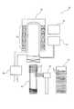
図1において、本発明の一実施形態にかかる基板処理装置10の概要を示す。基板処理装置10はいわゆるホットウォール式縦型減圧CVD装置である。
図1に示すように、ウェハカセット12により搬入されたウェハ(Si基板)aは、移載機14によりウェハカセット12からボート16へ移載される。全てのウェハaの移載が完了すると、ボート16は処理炉18内へ挿入され、処理炉18内は真空排気系20により減圧される。そしてヒータ22により処理炉18内を所望の温度に加熱し、温度が安定したところでガス供給系21から原料ガスとエッチングガスを交互に供給し、ウェハa上にSi又はSiGe等を選択エピタキシャル成長させる。なお、23は制御系であり、ボート16の処理炉18内への挿入及び回転、真空排気系20での排気、ガス供給系21からのガスの供給及びヒータ22による加熱等を制御する。Next, an embodiment of the present invention will be described with reference to the drawings.
In FIG. 1, the outline | summary of the
As shown in FIG. 1, the wafer (Si substrate) a carried in by the
Si又はSiGeの選択エピタキシャル成長の原料ガスとしては、SiH4やSi2H6、SiH2Cl2等のSi含有ガスが用いられ、SiGeの場合にはさらにGeH4やGeCl4等のGe含有ガスが加えられる。CVD反応において原料ガスが導入されるとSi上では直ちに成長が開始されるのに対してSiO2やSiN上では潜伏期間と呼ばれる成長の遅れが生じる。この潜伏期間の間、Si上のみにSiまたはSiGeを成長させるのが選択成長である。この選択成長中にはSiO2やSiN上にSi核の吸着が発生しており、選択性が損なわれることになる。そこで、原料ガスの供給後に、エッチングガスを供給してSiO2やSiN上に吸着したSi核の除去を行う。これを繰り返すことで選択エピタキシャル成長を行う。As a source gas for selective epitaxial growth of Si or SiGe, a Si-containing gas such as SiH4 , Si2 H6 , or SiH2 Cl2 is used. In the case of SiGe, a Ge-containing gas such as GeH4 or GeCl4 is further used. Added. When a source gas is introduced in the CVD reaction, growth starts immediately on Si, whereas a growth delay called a latent period occurs on SiO2 or SiN. During this incubation period, selective growth is to grow Si or SiGe only on Si. During this selective growth, adsorption of Si nuclei occurs on SiO2 or SiN, and the selectivity is impaired. Therefore, after supplying the source gas, an etching gas is supplied to remove Si nuclei adsorbed on SiO2 or SiN. By repeating this, selective epitaxial growth is performed.
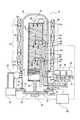
次に、本発明の一実施形態にかかる基板処理装置10に用いる処理炉18のボート16の挿入後の構成の詳細を、図面に基づいて説明する。
図2は本発明の一実施形態に係るボート16挿入後の処理炉18の概略構成図であり、縦断面図として示される。
図2に示すように、処理炉18には、処理室24を形成する、例えばアウターチューブよりなる反応管26と、反応管26の下部に配置され、排気口27から排気するガス排気管28と処理室24内に原料ガス等を供給する第1のガス供給管30とエッチングガス等を供給する第2のガス供給管32とが設けられ、反応管26とOリング33aを介して接続されたマニホールド34と、マニホールド34の下端部を閉塞し、処理室24をOリング33b及び33cを介して密閉するシールキャップ36と、ウェハ(Si基板)aを多段に保持(支持)するウェハ保持体(基板支持部材)としてのボート16と、ボート16を所定の回転数で回転させる回転機構38と、反応管26の外側に、図示しないヒータ素線と断熱部材よりなりウェハaを加熱するヒータ(加熱部材)22と、を備えている。Next, details of the configuration after insertion of the
FIG. 2 is a schematic configuration diagram of the
As shown in FIG. 2, the
反応管26は、例えば石英(SiO2)又は炭化シリコン(SiC)などの耐熱性材料からなり、上端が閉塞し、下端が開口した円筒形状に形成されている。マニホールド34は、例えばステンレス等からなり、上端及び下端が開口した円筒形状に形成されており、上端がOリング33aを介して反応管26と係合されており、第1のガス供給管30及び第2のガス供給管32がマニホールド34を貫通した状態で取り付けられている。シールキャップ36は、例えばステンレス等からなり、リング状部35と円盤状部37より形成され、マニホールド34の下端部をOリング33b及び33cを介して閉塞している。また、ボート16は、例えば石英や炭化シリコン等の耐熱性材料からなり、複数枚のウェハaを水平姿勢で且つ中心を揃えた状態で整列させて多段に保持するように構成されている。ボート16の回転機構38は、回転軸39がシールキャップ36を貫通してボート16に接続されており、ボート16を回転させることでウェハaを回転させるように構成されている。
また、ヒータ22は、上部ヒータ22A、中央上部ヒータ22B、中央ヒータ22C、中央下部ヒータ22D及び下部ヒータ22Eの5つの領域に分割されており、それらは、それぞれ円筒形状を有している。The
Further, the
そして、本発明の一実施形態に係る処理炉18内においては、ガス供給手段として、第1のガス供給管30から分岐された、高さの異なる第1のガス供給口40a、40b、40cを有する3本の第1のガス供給ノズル42a、42b、42cが配設されており、また、第1のガス供給ノズル42a、42b、42cとは別に、第2のガス供給管32から分岐された、高さの異なる第2のガス供給口43a、43b、43cを有する3本の第2のガス供給ノズル44a、44b、44cが配設されている。 And in the
この処理炉18の構成において、処理ガスは、例えば、原料ガス(例えばSiH4ガス)を供給する原料ガス供給源46、パージガス(例えばH2ガス)を供給するパージガス供給源48、エッチングガス(例えばCl2ガス)を供給するエッチングガス供給源50から供給される。成膜工程時には、原料ガス供給源46からの原料ガスのガス流量制御手段としての第1のMFC(マスフローコントローラ)52及びパージガス供給源48からのパージガスのガス流量制御手段としての第2のMFC54で流量が調節された後、原料ガスとパージガスが、それぞれ第1のガス供給管30及び第2のガス供給管32を通じて処理室24内に導かれる。そして、原料ガスが、第1のガス供給管30より分岐された第1のガス供給ノズル42a、42b、42cよりボート16の上部、中央部、下部の3箇所に供給され、パージガスが、第2のガス供給管32より分岐された第2のガス供給ノズル44a、44b、44cよりボート16の上部、中央部、下部の3箇所に供給される。In the configuration of the
またエッチング工程時には、パージガス供給源48からのパージガスのガス流量制御手段としての第3のMFC56及びエッチングガス供給源50からのエッチングガスのガス流量制御手段としての第4のMFC58で流量が調節された後、パージガスとエッチングガスが、それぞれ第1のガス供給管30及び第2のガス供給管32を通じて処理室24内に導かれる。そして、パージガスが、第1のガス供給管30より分岐された第1のガス供給ノズル42a、42b、42cよりボート16の上部、中央部、下部の3箇所に供給され、エッチングガスが、第2のガス供給管32より分岐された第2のガス供給ノズル44a、44b、44cよりボート16の上部、中央部、下部の3箇所に供給される。
また処理室24内の雰囲気は、ガス排気管28に接続された排気手段(例えば真空ポンプ59)により処理室24から排気される。Also, during the etching process, the flow rate was adjusted by the
The atmosphere in the
次に本発明の一実施形態に係る基板処理装置10によるウェハ処理の一例を説明する。
図2に示すように、未処理のウェハaを保持したボート16は、昇降モータ(図示省略)を駆動することにより、処理室24内に挿入される。次に制御装置60からの命令により排気バルブ62を開けて、処理室24内の雰囲気を排気し、処理室24内を減圧する。そして、制御装置60によりヒータ22を制御し、処理室24内の温度、ひいてはウェハaの温度を所望の温度に維持する。その後制御装置60からの命令により回転機構38が駆動され、ボート16を所定の回転数で回転させる。Next, an example of wafer processing by the
As shown in FIG. 2, the
そして制御装置60からの命令で、第1のMFC52、第2のMFC54の開度が調節された後、原料ガス供給源46からの原料ガスを供給するため開閉する第1のバルブ64及びパージガス供給源48からパージガスを供給するための第2のバルブ66を開く。そして第3のバルブ68を開き原料ガスが第1のガス供給管30及び第1のガス供給ノズル42a、42b、42cを通じて処理室24に導入され、ウェハaを処理する。それと同時に、第6のバルブ74を開き、パージガスが第2のガス供給管32及び第2のガス供給ノズル44a、44b、44cを通じて処理室24に導入される。 Then, after the opening degree of the
次に、制御装置60からの命令で第3のMFC56、第4のMFC58の開度が調節された後、エッチングガス供給源50からのエッチングガスを供給するため開閉する第4のバルブ70及びパージガス供給源48からパージガスを供給するための第5のバルブ72を開く。そして、第6のバルブ74を開き、エッチングガスが第2のガス供給管32及び第2のガス供給ノズル44a、44b、44cを通じて処理室24に導入され、ウェハaを処理する。それと同時に、第3のバルブ68を開き、パージガスが第1のガス供給管30及び第1のガス供給ノズル42a、42b、42cを通じて処理室24に導入される。 Next, after the opening degree of the
上記のように、本発明の一実施形態における基板処理装置10においては、原料ガスを処理室24内に供給する第1のガス供給管30及び第1のガス供給ノズル42a、42b、42cと、エッチングガスを処理室24内に供給する第2のガス供給管32及び第2のガス供給ノズル44a、44b、44cと、を分離している。したがって、従来の温度勾配を設ける場合では、成長速度とエッチング速度のどちらか一方しか調整することができなかったが、本発明の一実施形態における基板処理装置10では原料ガス及びエッチングガスがそれぞれ別の複数本のノズルから供給されるため、その供給量を調節することで成長速度とエッチング速度の両方の調整が可能となる。 As described above, in the
また、同じノズルから原料ガスとエッチングガスを供給した場合、原料ガスの自己分解によりノズル内に膜がつき、そこにエッチングガスを流すと、パーティクルやエッチングガスの消費が生じていた。それに対し、本発明の一実施形態における基板処理装置10においては、原料ガスとエッチングガスをそれぞれ別の複数本のノズルから供給しているため、ノズルからのパーティクル発生を回避することができる。またエッチングガスを供給する第2のガス供給ノズル44a、44b、44cの内壁に膜が付着しないため、第2のガス供給ノズル44a、44b、44c内でエッチングガスが消費されることがなく、より良好なエッチング特性を得ることができ、ウェハaに対して第1のガス供給ノズル42a、42b、42c及び第2のガス供給ノズル44a、44b、44cの内壁状態によらずに安定したエッチングレートを確保することができる。 Further, when the source gas and the etching gas are supplied from the same nozzle, a film is formed in the nozzle due to the self-decomposition of the source gas, and if the etching gas is flowed there, particles and etching gas are consumed. On the other hand, in the
さらに、本発明の一実施形態における基板処理装置10においては、各ガスごとに高さの異なる複数本のノズルを設けてそこからガスを供給しているため、反応ガスの消費によって排気側(処理炉18内下部)ほど成長速度が低下するのを、処理炉18の上部と下部の間におけるガスの途中供給によって調整することができ、これにより処理温度上限に近い温度での成長速度を基準とすることができ、温度勾配を設ける場合よりも成長速度を大きくすることができる。 Furthermore, in the
なお、上記のように成膜(原料ガス供給)中、エッチングガス用の第2のガス供給ノズル44a、44b、44cに水素ガス等のパージガスを流通させることによって、第2のガス供給ノズル44a、44b、44c内へのガスの侵入と内壁への膜付着を防止することができる。また同様に、エッチング(エッチングガス供給)中は原料ガス用の第1のガス供給ノズル42a、42b、42cにパージガスを流通させることによって第1のガス供給ノズル42a、42b、42c内へのエッチングガスの侵入を防止できる。 During film formation (source gas supply) as described above, the second
次に一例として、本発明の一実施形態に係る基板処理装置10を用いたSi膜の選択エピタキシャル成長の具体的な工程の流れを図3に基づいて説明する。 Next, as an example, a specific process flow of selective epitaxial growth of a Si film using the
(1)まず、原料ガスであるモノシラン(SiH4)ガスを第1のガス供給管30及び第1のガス供給ノズル42a、42b、42cを通じて処理室24に供給する(成膜工程)。その際、パージガスである水素(H2)ガスを第2のガス供給管32及び第2のガス供給ノズル44a、44b、44cを通じて処理室24に供給する。
(2)次に、ガスの供給を止めて処理室24内の排気を行う。
(3)続いてパージガスであるH2ガスを、第1のガス供給管及び第1のガス供給ノズル42a、42b、42cと、第2のガス供給管32及び第2のガス供給ノズル44a、44b、44cと、の両方を通じて処理室24に供給する(パージ工程)。
(4)その後、エッチングガスである塩素(Cl2)ガスを第2のガス供給管32及び第2のガス供給ノズル44a、44b、44cを通じて処理室24に供給する(エッチング工程)。その際にパージガスであるH2ガスを第1のガス供給管30及び第1のガス供給ノズル42a、42b、42cを通じて処理室24内に供給する。
(5)その後、ガスの供給を止めて処理室24内の排気を行う。
(6)そして、パージガスであるH2ガスを第1のガス供給管30及び第1のガス供給ノズル42a、42b、42cと、第2のガス供給管32及び第2のガス供給ノズル44a、44b、44cと、の両方を通じて処理室24に供給する(パージ工程)。
以上の(1)〜(6)の工程を1サイクルとし、これらの工程を繰り返してウェハa上でのSi膜の選択エピタキシャル成長を行うことで、成長速度とエッチング速度の両方を調整することが可能となるとともに、パーティクル発生を回避でき、良好なエッチング特性を得ることができる。(1) First, monosilane (SiH4 ) gas, which is a raw material gas, is supplied to the
(2) Next, the gas supply is stopped and the
(3) Subsequently, the H2 gas as the purge gas is supplied to the first gas supply pipe and the first
(4) Thereafter, chlorine (Cl2 ) gas, which is an etching gas, is supplied to the
(5) Thereafter, the gas supply is stopped and the
(6) Then, the H2 gas which is the purge gas is supplied to the first gas supply pipe 30 and the first
It is possible to adjust both the growth rate and the etching rate by repeating the above steps (1) to (6) as one cycle and repeating these steps to perform selective epitaxial growth of the Si film on the wafer a. In addition, the generation of particles can be avoided, and good etching characteristics can be obtained.
以上述べたように、本発明によれば、Si又はSiGeの選択エピタキシャル成長の成長速度とエッチング速度の両方を調整することが可能となり、ノズルからのパーティクル発生を回避でき、良好なエッチング特性を得ることが可能となる基板処理装置を提供することが可能となる。 As described above, according to the present invention, it is possible to adjust both the growth rate and the etching rate of selective epitaxial growth of Si or SiGe, avoid the generation of particles from the nozzle, and obtain good etching characteristics. It is possible to provide a substrate processing apparatus that can perform the above.
10 基板処理装置
12 ウェハカセット
14 移載機
16 ボート
18 処理炉
20 真空排気系
22 ヒータ
24 処理室
26 反応管
27 排気口
28 ガス排気管
30 第1のガス供給管
32 第2のガス供給管
33a、33b Oリング
34 マニホールド
35 リング状部
36 シールキャップ
37 円板状部
38 回転機構
40a、40b、40c 第1のガス供給口
42a、42b、42c 第1のガス供給ノズル
43a、43b、43c 第2のガス供給口
44a、44b、44c 第2のガス供給ノズル
46 原料ガス供給源
48 パージガス供給源
50 エッチングガス供給源
52 第1のMFC
54 第2のMFC
56 第3のMFC
58 第4のMFC
59 真空ポンプ
60 制御装置
62 排気バルブ
64 第1のバルブ
66 第2のバルブ
68 第3のバルブ
70 第4のバルブ
72 第5のバルブ
74 第6のバルブDESCRIPTION OF
54 Second MFC
56 Third MFC
58 Fourth MFC
59
Claims (4)
Translated fromJapanese前記Si含有ガスと前記Cl2ガスとを交互に繰り返して処理室内に供給して前記処理室内に収容された基板の表面に選択的にエピタキシャル膜を成長させる基板処理装置であって、
前記処理室内で前記基板を支持する基板支持部材と、
前記基板及び前記処理室内の雰囲気を加熱し、前記処理室の外部に設けられる加熱部材と、
前記処理室内に配置され、前記処理室内のそれぞれ異なる複数の高さへ開口するガス供給孔を有する複数の第1のガス供給ノズル及び前記処理室内のそれぞれ異なる複数の高さへ開口するガス供給孔を有する複数の第2のガス供給ノズルを含むガス供給系と、
前記処理室に開口する排気口と、
を備え、
前記ガス供給系は、前記Si含有ガスを供給する第1のガス供給管と、前記Cl2ガスを供給する前記第1のガス供給管とは異なる第2のガス供給管とからなり、
前記複数の第1のガス供給ノズルは、前記第1のガス供給管から分岐され、前記複数の第2のガス供給ノズルは、前記第2のガス供給管から分岐されたことを特徴とする基板処理装置。Use at least Si-containing gas and Cl2 gas,
A substrate processing apparatus for alternately growing the Si-containing gas and the Cl2 gas to be supplied into a processing chamber and selectively growing an epitaxial film on the surface of the substrate housed in the processing chamber,
A substrate support member for supporting the substrate in the processing chamber;
Heating the atmosphere in the processing chamber and the substrate, and a heating member provided outside the processing chamber;
A plurality of first gas supply nozzles arranged in the processing chamber and having gas supply holes that open to a plurality of different heights in the processing chamber, and gas supply holes that open to a plurality of different heights in the processing chamber. A gas supply system including a plurality of second gas supply nozzles,
An exhaust opening that opens into the processing chamber;
With
The gas supply system includes a first gas supplypipe for supplying the Si-containing gas,it consists of a different, second gas supplypipe from the first gas supplypipe for supplying the Cl2gas,
The plurality of first gas supply nozzles are branched from the first gas supply pipe, and the plurality of second gas supply nozzles are branched from the second gas supply pipe. Processing equipment.
前記複数の第1のガス供給ノズルを用いて前記Si含有ガスを処理室内に供給し、前記複数の第2のガス供給ノズルを用いてパージガスを処理室内に供給する成膜工程と、
前記Si含有ガスの供給を止めて前記処理室内の雰囲気を排気する排気工程と、
前記複数の第1のガス供給ノズル及び前記複数の第2のガス供給ノズルを用いてパージガスを処理室内に供給するパージ工程と、
前記複数の第2のガス供給ノズルを用いてエッチングガスとしてCl含有ガスを処理室内に供給し、前記複数の第1のガス供給ノズルを用いてパージガスを処理室内に供給するエッチング工程と、
前記Cl含有ガスの供給を止めて前記処理室内の雰囲気を排気する排気工程と、
前記複数の第1のガス供給ノズル及び前記複数の第2のガス供給ノズルを用いてパージガスを処理室内に供給するパージ工程と、
を繰り返して所望の膜厚を成長させることを特徴とする選択エピタキシャル膜成長方法。A plurality of first gas supply nozzles for supplying Si-containing gas to a plurality of different heights in the processing chamber, and a plurality of second gases for supplying a Cl-containing gas to a plurality of different heights in the processing chamber. In a substrate processing apparatus including a supply nozzle, a selective epitaxial film growth method for selectively growing an epitaxial film on a surface of a substrate housed in a processing chamber, at least,
A film forming step of supplying the Si-containing gas into a processing chamber using the plurality of first gas supply nozzles, and supplying a purge gas into the processing chamber using the plurality of second gas supply nozzles;
An exhaust process for stopping the supply of the Si-containing gas and exhausting the atmosphere in the processing chamber;
A purge step of supplying a purge gas into the processing chamber using the plurality of first gas supply nozzles and the plurality of second gas supply nozzles;
An etching step of supplying a Cl-containing gas as an etching gas into the processing chamber using the plurality of second gas supply nozzles, and supplying a purge gas into the processing chamber using the plurality of first gas supply nozzles;
An exhaust process for stopping the supply of the Cl-containing gas and exhausting the atmosphere in the processing chamber;
A purge step of supplying a purge gas into the processing chamber using the plurality of first gas supply nozzles and the plurality of second gas supply nozzles;
To grow a desired film thickness by repeating the above steps.
Priority Applications (3)
| Application Number | Priority Date | Filing Date | Title |
|---|---|---|---|
| JP2006304936AJP4464949B2 (en) | 2006-11-10 | 2006-11-10 | Substrate processing apparatus and selective epitaxial film growth method |
| US11/979,816US20080135516A1 (en) | 2006-11-10 | 2007-11-08 | Substrate treatment device |
| US13/067,117US8652258B2 (en) | 2006-11-10 | 2011-05-10 | Substrate treatment device |
Applications Claiming Priority (1)
| Application Number | Priority Date | Filing Date | Title |
|---|---|---|---|
| JP2006304936AJP4464949B2 (en) | 2006-11-10 | 2006-11-10 | Substrate processing apparatus and selective epitaxial film growth method |
Publications (2)
| Publication Number | Publication Date |
|---|---|
| JP2008124181A JP2008124181A (en) | 2008-05-29 |
| JP4464949B2true JP4464949B2 (en) | 2010-05-19 |
Family
ID=39496741
Family Applications (1)
| Application Number | Title | Priority Date | Filing Date |
|---|---|---|---|
| JP2006304936AActiveJP4464949B2 (en) | 2006-11-10 | 2006-11-10 | Substrate processing apparatus and selective epitaxial film growth method |
Country Status (2)
| Country | Link |
|---|---|
| US (2) | US20080135516A1 (en) |
| JP (1) | JP4464949B2 (en) |
Cited By (1)
| Publication number | Priority date | Publication date | Assignee | Title |
|---|---|---|---|---|
| US12371788B2 (en) | 2019-03-25 | 2025-07-29 | Kokusai Electric Corporation | Method of manufacturing semiconductor device, substrate processing apparatus and non-transitory computer-readable recording medium |
Families Citing this family (238)
| Publication number | Priority date | Publication date | Assignee | Title |
|---|---|---|---|---|
| JP4464949B2 (en)* | 2006-11-10 | 2010-05-19 | 株式会社日立国際電気 | Substrate processing apparatus and selective epitaxial film growth method |
| KR101623458B1 (en)* | 2008-03-26 | 2016-05-23 | 지티에이티 코포레이션 | Systems and methods for distributing gas in a chemical vapor deposition reactor |
| JP5645718B2 (en)* | 2011-03-07 | 2014-12-24 | 東京エレクトロン株式会社 | Heat treatment equipment |
| US20130023129A1 (en) | 2011-07-20 | 2013-01-24 | Asm America, Inc. | Pressure transmitter for a semiconductor processing environment |
| JP6002312B2 (en)* | 2012-03-28 | 2016-10-05 | クックジェ エレクトリック コリア カンパニー リミテッド | Equipment and cluster equipment for selective epitaxial growth |
| US8785303B2 (en) | 2012-06-01 | 2014-07-22 | Taiwan Semiconductor Manufacturing Company, Ltd. | Methods for depositing amorphous silicon |
| US20160376700A1 (en) | 2013-02-01 | 2016-12-29 | Asm Ip Holding B.V. | System for treatment of deposition reactor |
| WO2014125653A1 (en)* | 2013-02-15 | 2014-08-21 | 株式会社日立国際電気 | Substrate processing device, method of producing semiconductor device and substrate processing method |
| US10941490B2 (en) | 2014-10-07 | 2021-03-09 | Asm Ip Holding B.V. | Multiple temperature range susceptor, assembly, reactor and system including the susceptor, and methods of using the same |
| US10276355B2 (en) | 2015-03-12 | 2019-04-30 | Asm Ip Holding B.V. | Multi-zone reactor, system including the reactor, and method of using the same |
| US11139308B2 (en) | 2015-12-29 | 2021-10-05 | Asm Ip Holding B.V. | Atomic layer deposition of III-V compounds to form V-NAND devices |
| US10529554B2 (en) | 2016-02-19 | 2020-01-07 | Asm Ip Holding B.V. | Method for forming silicon nitride film selectively on sidewalls or flat surfaces of trenches |
| US10343920B2 (en) | 2016-03-18 | 2019-07-09 | Asm Ip Holding B.V. | Aligned carbon nanotubes |
| US11453943B2 (en) | 2016-05-25 | 2022-09-27 | Asm Ip Holding B.V. | Method for forming carbon-containing silicon/metal oxide or nitride film by ALD using silicon precursor and hydrocarbon precursor |
| KR102326377B1 (en)* | 2016-06-07 | 2021-11-15 | 가부시키가이샤 코쿠사이 엘렉트릭 | Substrate processing apparatus, method of manufacturing semiconductor device and program |
| US10612137B2 (en) | 2016-07-08 | 2020-04-07 | Asm Ip Holdings B.V. | Organic reactants for atomic layer deposition |
| US9859151B1 (en) | 2016-07-08 | 2018-01-02 | Asm Ip Holding B.V. | Selective film deposition method to form air gaps |
| US9887082B1 (en) | 2016-07-28 | 2018-02-06 | Asm Ip Holding B.V. | Method and apparatus for filling a gap |
| US9812320B1 (en) | 2016-07-28 | 2017-11-07 | Asm Ip Holding B.V. | Method and apparatus for filling a gap |
| US11532757B2 (en) | 2016-10-27 | 2022-12-20 | Asm Ip Holding B.V. | Deposition of charge trapping layers |
| US10714350B2 (en) | 2016-11-01 | 2020-07-14 | ASM IP Holdings, B.V. | Methods for forming a transition metal niobium nitride film on a substrate by atomic layer deposition and related semiconductor device structures |
| KR101960763B1 (en)* | 2016-11-03 | 2019-03-21 | 주식회사 유진테크 | Method for manufacturing an epitaxial layer in low temperature |
| KR102546317B1 (en) | 2016-11-15 | 2023-06-21 | 에이에스엠 아이피 홀딩 비.브이. | Gas supply unit and substrate processing apparatus including the same |
| US11447861B2 (en) | 2016-12-15 | 2022-09-20 | Asm Ip Holding B.V. | Sequential infiltration synthesis apparatus and a method of forming a patterned structure |
| US11581186B2 (en) | 2016-12-15 | 2023-02-14 | Asm Ip Holding B.V. | Sequential infiltration synthesis apparatus |
| US11390950B2 (en) | 2017-01-10 | 2022-07-19 | Asm Ip Holding B.V. | Reactor system and method to reduce residue buildup during a film deposition process |
| US10468261B2 (en) | 2017-02-15 | 2019-11-05 | Asm Ip Holding B.V. | Methods for forming a metallic film on a substrate by cyclical deposition and related semiconductor device structures |
| JP6847202B2 (en)* | 2017-03-31 | 2021-03-24 | 株式会社Kokusai Electric | Semiconductor device manufacturing methods, substrate processing devices and programs |
| US10770286B2 (en) | 2017-05-08 | 2020-09-08 | Asm Ip Holdings B.V. | Methods for selectively forming a silicon nitride film on a substrate and related semiconductor device structures |
| US12040200B2 (en) | 2017-06-20 | 2024-07-16 | Asm Ip Holding B.V. | Semiconductor processing apparatus and methods for calibrating a semiconductor processing apparatus |
| US11306395B2 (en) | 2017-06-28 | 2022-04-19 | Asm Ip Holding B.V. | Methods for depositing a transition metal nitride film on a substrate by atomic layer deposition and related deposition apparatus |
| KR20190009245A (en) | 2017-07-18 | 2019-01-28 | 에이에스엠 아이피 홀딩 비.브이. | Methods for forming a semiconductor device structure and related semiconductor device structures |
| US11374112B2 (en) | 2017-07-19 | 2022-06-28 | Asm Ip Holding B.V. | Method for depositing a group IV semiconductor and related semiconductor device structures |
| US10590535B2 (en) | 2017-07-26 | 2020-03-17 | Asm Ip Holdings B.V. | Chemical treatment, deposition and/or infiltration apparatus and method for using the same |
| TWI815813B (en) | 2017-08-04 | 2023-09-21 | 荷蘭商Asm智慧財產控股公司 | Showerhead assembly for distributing a gas within a reaction chamber |
| US10692741B2 (en) | 2017-08-08 | 2020-06-23 | Asm Ip Holdings B.V. | Radiation shield |
| US10770336B2 (en) | 2017-08-08 | 2020-09-08 | Asm Ip Holding B.V. | Substrate lift mechanism and reactor including same |
| US11769682B2 (en) | 2017-08-09 | 2023-09-26 | Asm Ip Holding B.V. | Storage apparatus for storing cassettes for substrates and processing apparatus equipped therewith |
| US11830730B2 (en) | 2017-08-29 | 2023-11-28 | Asm Ip Holding B.V. | Layer forming method and apparatus |
| US11295980B2 (en) | 2017-08-30 | 2022-04-05 | Asm Ip Holding B.V. | Methods for depositing a molybdenum metal film over a dielectric surface of a substrate by a cyclical deposition process and related semiconductor device structures |
| US10658205B2 (en) | 2017-09-28 | 2020-05-19 | Asm Ip Holdings B.V. | Chemical dispensing apparatus and methods for dispensing a chemical to a reaction chamber |
| US10403504B2 (en) | 2017-10-05 | 2019-09-03 | Asm Ip Holding B.V. | Method for selectively depositing a metallic film on a substrate |
| US10923344B2 (en) | 2017-10-30 | 2021-02-16 | Asm Ip Holding B.V. | Methods for forming a semiconductor structure and related semiconductor structures |
| CN111344522B (en) | 2017-11-27 | 2022-04-12 | 阿斯莫Ip控股公司 | Including clean mini-environment device |
| WO2019103613A1 (en) | 2017-11-27 | 2019-05-31 | Asm Ip Holding B.V. | A storage device for storing wafer cassettes for use with a batch furnace |
| US10872771B2 (en) | 2018-01-16 | 2020-12-22 | Asm Ip Holding B. V. | Method for depositing a material film on a substrate within a reaction chamber by a cyclical deposition process and related device structures |
| TWI799494B (en) | 2018-01-19 | 2023-04-21 | 荷蘭商Asm 智慧財產控股公司 | Deposition method |
| KR102695659B1 (en) | 2018-01-19 | 2024-08-14 | 에이에스엠 아이피 홀딩 비.브이. | Method for depositing a gap filling layer by plasma assisted deposition |
| US11081345B2 (en) | 2018-02-06 | 2021-08-03 | Asm Ip Holding B.V. | Method of post-deposition treatment for silicon oxide film |
| WO2019158960A1 (en) | 2018-02-14 | 2019-08-22 | Asm Ip Holding B.V. | A method for depositing a ruthenium-containing film on a substrate by a cyclical deposition process |
| US10896820B2 (en) | 2018-02-14 | 2021-01-19 | Asm Ip Holding B.V. | Method for depositing a ruthenium-containing film on a substrate by a cyclical deposition process |
| US10731249B2 (en) | 2018-02-15 | 2020-08-04 | Asm Ip Holding B.V. | Method of forming a transition metal containing film on a substrate by a cyclical deposition process, a method for supplying a transition metal halide compound to a reaction chamber, and related vapor deposition apparatus |
| KR102636427B1 (en) | 2018-02-20 | 2024-02-13 | 에이에스엠 아이피 홀딩 비.브이. | Substrate processing method and apparatus |
| US10975470B2 (en) | 2018-02-23 | 2021-04-13 | Asm Ip Holding B.V. | Apparatus for detecting or monitoring for a chemical precursor in a high temperature environment |
| US11473195B2 (en) | 2018-03-01 | 2022-10-18 | Asm Ip Holding B.V. | Semiconductor processing apparatus and a method for processing a substrate |
| KR102646467B1 (en) | 2018-03-27 | 2024-03-11 | 에이에스엠 아이피 홀딩 비.브이. | Method of forming an electrode on a substrate and a semiconductor device structure including an electrode |
| KR102600229B1 (en) | 2018-04-09 | 2023-11-10 | 에이에스엠 아이피 홀딩 비.브이. | Substrate supporting device, substrate processing apparatus including the same and substrate processing method |
| US12025484B2 (en) | 2018-05-08 | 2024-07-02 | Asm Ip Holding B.V. | Thin film forming method |
| US12272527B2 (en) | 2018-05-09 | 2025-04-08 | Asm Ip Holding B.V. | Apparatus for use with hydrogen radicals and method of using same |
| KR102596988B1 (en) | 2018-05-28 | 2023-10-31 | 에이에스엠 아이피 홀딩 비.브이. | Method of processing a substrate and a device manufactured by the same |
| US11718913B2 (en) | 2018-06-04 | 2023-08-08 | Asm Ip Holding B.V. | Gas distribution system and reactor system including same |
| KR102568797B1 (en) | 2018-06-21 | 2023-08-21 | 에이에스엠 아이피 홀딩 비.브이. | Substrate processing system |
| US10797133B2 (en) | 2018-06-21 | 2020-10-06 | Asm Ip Holding B.V. | Method for depositing a phosphorus doped silicon arsenide film and related semiconductor device structures |
| TWI873894B (en) | 2018-06-27 | 2025-02-21 | 荷蘭商Asm Ip私人控股有限公司 | Cyclic deposition methods for forming metal-containing material and films and structures including the metal-containing material |
| KR102854019B1 (en) | 2018-06-27 | 2025-09-02 | 에이에스엠 아이피 홀딩 비.브이. | Periodic deposition method for forming a metal-containing material and films and structures comprising the metal-containing material |
| US10755922B2 (en) | 2018-07-03 | 2020-08-25 | Asm Ip Holding B.V. | Method for depositing silicon-free carbon-containing film as gap-fill layer by pulse plasma-assisted deposition |
| US10388513B1 (en) | 2018-07-03 | 2019-08-20 | Asm Ip Holding B.V. | Method for depositing silicon-free carbon-containing film as gap-fill layer by pulse plasma-assisted deposition |
| US11430674B2 (en) | 2018-08-22 | 2022-08-30 | Asm Ip Holding B.V. | Sensor array, apparatus for dispensing a vapor phase reactant to a reaction chamber and related methods |
| KR102707956B1 (en) | 2018-09-11 | 2024-09-19 | 에이에스엠 아이피 홀딩 비.브이. | Method for deposition of a thin film |
| US11024523B2 (en) | 2018-09-11 | 2021-06-01 | Asm Ip Holding B.V. | Substrate processing apparatus and method |
| CN110970344B (en) | 2018-10-01 | 2024-10-25 | Asmip控股有限公司 | Substrate holding apparatus, system comprising the same and method of using the same |
| KR102592699B1 (en) | 2018-10-08 | 2023-10-23 | 에이에스엠 아이피 홀딩 비.브이. | Substrate support unit and apparatuses for depositing thin film and processing the substrate including the same |
| KR102546322B1 (en) | 2018-10-19 | 2023-06-21 | 에이에스엠 아이피 홀딩 비.브이. | Substrate processing apparatus and substrate processing method |
| US12378665B2 (en) | 2018-10-26 | 2025-08-05 | Asm Ip Holding B.V. | High temperature coatings for a preclean and etch apparatus and related methods |
| US11087997B2 (en) | 2018-10-31 | 2021-08-10 | Asm Ip Holding B.V. | Substrate processing apparatus for processing substrates |
| KR102748291B1 (en) | 2018-11-02 | 2024-12-31 | 에이에스엠 아이피 홀딩 비.브이. | Substrate support unit and substrate processing apparatus including the same |
| US11572620B2 (en) | 2018-11-06 | 2023-02-07 | Asm Ip Holding B.V. | Methods for selectively depositing an amorphous silicon film on a substrate |
| US10818758B2 (en) | 2018-11-16 | 2020-10-27 | Asm Ip Holding B.V. | Methods for forming a metal silicate film on a substrate in a reaction chamber and related semiconductor device structures |
| US12040199B2 (en) | 2018-11-28 | 2024-07-16 | Asm Ip Holding B.V. | Substrate processing apparatus for processing substrates |
| KR102636428B1 (en) | 2018-12-04 | 2024-02-13 | 에이에스엠 아이피 홀딩 비.브이. | A method for cleaning a substrate processing apparatus |
| US11158513B2 (en) | 2018-12-13 | 2021-10-26 | Asm Ip Holding B.V. | Methods for forming a rhenium-containing film on a substrate by a cyclical deposition process and related semiconductor device structures |
| TWI874340B (en) | 2018-12-14 | 2025-03-01 | 荷蘭商Asm Ip私人控股有限公司 | Method of forming device structure, structure formed by the method and system for performing the method |
| TWI866480B (en) | 2019-01-17 | 2024-12-11 | 荷蘭商Asm Ip 私人控股有限公司 | Methods of forming a transition metal containing film on a substrate by a cyclical deposition process |
| TWI838458B (en) | 2019-02-20 | 2024-04-11 | 荷蘭商Asm Ip私人控股有限公司 | Apparatus and methods for plug fill deposition in 3-d nand applications |
| TWI845607B (en) | 2019-02-20 | 2024-06-21 | 荷蘭商Asm Ip私人控股有限公司 | Cyclical deposition method and apparatus for filling a recess formed within a substrate surface |
| TWI873122B (en) | 2019-02-20 | 2025-02-21 | 荷蘭商Asm Ip私人控股有限公司 | Method of filling a recess formed within a surface of a substrate, semiconductor structure formed according to the method, and semiconductor processing apparatus |
| TWI842826B (en) | 2019-02-22 | 2024-05-21 | 荷蘭商Asm Ip私人控股有限公司 | Substrate processing apparatus and method for processing substrate |
| KR102858005B1 (en) | 2019-03-08 | 2025-09-09 | 에이에스엠 아이피 홀딩 비.브이. | Method for Selective Deposition of Silicon Nitride Layer and Structure Including Selectively-Deposited Silicon Nitride Layer |
| US11742198B2 (en) | 2019-03-08 | 2023-08-29 | Asm Ip Holding B.V. | Structure including SiOCN layer and method of forming same |
| JP2020167398A (en) | 2019-03-28 | 2020-10-08 | エーエスエム・アイピー・ホールディング・ベー・フェー | Door openers and substrate processing equipment provided with door openers |
| KR102809999B1 (en) | 2019-04-01 | 2025-05-19 | 에이에스엠 아이피 홀딩 비.브이. | Method of manufacturing semiconductor device |
| KR20200123380A (en) | 2019-04-19 | 2020-10-29 | 에이에스엠 아이피 홀딩 비.브이. | Layer forming method and apparatus |
| KR20200125453A (en) | 2019-04-24 | 2020-11-04 | 에이에스엠 아이피 홀딩 비.브이. | Gas-phase reactor system and method of using same |
| KR20200130121A (en) | 2019-05-07 | 2020-11-18 | 에이에스엠 아이피 홀딩 비.브이. | Chemical source vessel with dip tube |
| KR20200130652A (en) | 2019-05-10 | 2020-11-19 | 에이에스엠 아이피 홀딩 비.브이. | Method of depositing material onto a surface and structure formed according to the method |
| JP7612342B2 (en) | 2019-05-16 | 2025-01-14 | エーエスエム・アイピー・ホールディング・ベー・フェー | Wafer boat handling apparatus, vertical batch furnace and method |
| JP7598201B2 (en) | 2019-05-16 | 2024-12-11 | エーエスエム・アイピー・ホールディング・ベー・フェー | Wafer boat handling apparatus, vertical batch furnace and method |
| USD975665S1 (en) | 2019-05-17 | 2023-01-17 | Asm Ip Holding B.V. | Susceptor shaft |
| USD947913S1 (en) | 2019-05-17 | 2022-04-05 | Asm Ip Holding B.V. | Susceptor shaft |
| KR20200141002A (en) | 2019-06-06 | 2020-12-17 | 에이에스엠 아이피 홀딩 비.브이. | Method of using a gas-phase reactor system including analyzing exhausted gas |
| KR20200141931A (en) | 2019-06-10 | 2020-12-21 | 에이에스엠 아이피 홀딩 비.브이. | Method for cleaning quartz epitaxial chambers |
| KR20200143254A (en) | 2019-06-11 | 2020-12-23 | 에이에스엠 아이피 홀딩 비.브이. | Method of forming an electronic structure using an reforming gas, system for performing the method, and structure formed using the method |
| KR20210005515A (en) | 2019-07-03 | 2021-01-14 | 에이에스엠 아이피 홀딩 비.브이. | Temperature control assembly for substrate processing apparatus and method of using same |
| JP7499079B2 (en) | 2019-07-09 | 2024-06-13 | エーエスエム・アイピー・ホールディング・ベー・フェー | Plasma device using coaxial waveguide and substrate processing method |
| CN112216646A (en) | 2019-07-10 | 2021-01-12 | Asm Ip私人控股有限公司 | Substrate supporting assembly and substrate processing device comprising same |
| KR20210010307A (en) | 2019-07-16 | 2021-01-27 | 에이에스엠 아이피 홀딩 비.브이. | Substrate processing apparatus |
| KR102860110B1 (en) | 2019-07-17 | 2025-09-16 | 에이에스엠 아이피 홀딩 비.브이. | Methods of forming silicon germanium structures |
| KR20210010816A (en) | 2019-07-17 | 2021-01-28 | 에이에스엠 아이피 홀딩 비.브이. | Radical assist ignition plasma system and method |
| US11643724B2 (en) | 2019-07-18 | 2023-05-09 | Asm Ip Holding B.V. | Method of forming structures using a neutral beam |
| KR20210010817A (en) | 2019-07-19 | 2021-01-28 | 에이에스엠 아이피 홀딩 비.브이. | Method of Forming Topology-Controlled Amorphous Carbon Polymer Film |
| TWI851767B (en) | 2019-07-29 | 2024-08-11 | 荷蘭商Asm Ip私人控股有限公司 | Methods for selective deposition utilizing n-type dopants and/or alternative dopants to achieve high dopant incorporation |
| CN112309899A (en) | 2019-07-30 | 2021-02-02 | Asm Ip私人控股有限公司 | Substrate processing apparatus |
| CN112309900A (en) | 2019-07-30 | 2021-02-02 | Asm Ip私人控股有限公司 | Substrate processing apparatus |
| US12169361B2 (en) | 2019-07-30 | 2024-12-17 | Asm Ip Holding B.V. | Substrate processing apparatus and method |
| US11587815B2 (en) | 2019-07-31 | 2023-02-21 | Asm Ip Holding B.V. | Vertical batch furnace assembly |
| US11587814B2 (en) | 2019-07-31 | 2023-02-21 | Asm Ip Holding B.V. | Vertical batch furnace assembly |
| US11227782B2 (en) | 2019-07-31 | 2022-01-18 | Asm Ip Holding B.V. | Vertical batch furnace assembly |
| CN112323048B (en) | 2019-08-05 | 2024-02-09 | Asm Ip私人控股有限公司 | Liquid level sensor for chemical source container |
| CN112342526A (en) | 2019-08-09 | 2021-02-09 | Asm Ip私人控股有限公司 | Heater assembly including cooling device and method of using same |
| USD965044S1 (en) | 2019-08-19 | 2022-09-27 | Asm Ip Holding B.V. | Susceptor shaft |
| USD965524S1 (en) | 2019-08-19 | 2022-10-04 | Asm Ip Holding B.V. | Susceptor support |
| JP2021031769A (en) | 2019-08-21 | 2021-03-01 | エーエスエム アイピー ホールディング ビー.ブイ. | Production apparatus of mixed gas of film deposition raw material and film deposition apparatus |
| KR20210024423A (en) | 2019-08-22 | 2021-03-05 | 에이에스엠 아이피 홀딩 비.브이. | Method for forming a structure with a hole |
| USD979506S1 (en) | 2019-08-22 | 2023-02-28 | Asm Ip Holding B.V. | Insulator |
| KR20210024420A (en) | 2019-08-23 | 2021-03-05 | 에이에스엠 아이피 홀딩 비.브이. | Method for depositing silicon oxide film having improved quality by peald using bis(diethylamino)silane |
| US11286558B2 (en) | 2019-08-23 | 2022-03-29 | Asm Ip Holding B.V. | Methods for depositing a molybdenum nitride film on a surface of a substrate by a cyclical deposition process and related semiconductor device structures including a molybdenum nitride film |
| KR102806450B1 (en) | 2019-09-04 | 2025-05-12 | 에이에스엠 아이피 홀딩 비.브이. | Methods for selective deposition using a sacrificial capping layer |
| KR102733104B1 (en) | 2019-09-05 | 2024-11-22 | 에이에스엠 아이피 홀딩 비.브이. | Substrate processing apparatus |
| US11562901B2 (en) | 2019-09-25 | 2023-01-24 | Asm Ip Holding B.V. | Substrate processing method |
| CN112593212B (en) | 2019-10-02 | 2023-12-22 | Asm Ip私人控股有限公司 | Method for forming topologically selective silicon oxide film by cyclic plasma enhanced deposition process |
| KR20210042810A (en) | 2019-10-08 | 2021-04-20 | 에이에스엠 아이피 홀딩 비.브이. | Reactor system including a gas distribution assembly for use with activated species and method of using same |
| TW202128273A (en) | 2019-10-08 | 2021-08-01 | 荷蘭商Asm Ip私人控股有限公司 | Gas injection system, reactor system, and method of depositing material on surface of substratewithin reaction chamber |
| TWI846953B (en) | 2019-10-08 | 2024-07-01 | 荷蘭商Asm Ip私人控股有限公司 | Substrate processing device |
| TWI846966B (en) | 2019-10-10 | 2024-07-01 | 荷蘭商Asm Ip私人控股有限公司 | Method of forming a photoresist underlayer and structure including same |
| US12009241B2 (en) | 2019-10-14 | 2024-06-11 | Asm Ip Holding B.V. | Vertical batch furnace assembly with detector to detect cassette |
| TWI834919B (en) | 2019-10-16 | 2024-03-11 | 荷蘭商Asm Ip私人控股有限公司 | Method of topology-selective film formation of silicon oxide |
| US11637014B2 (en) | 2019-10-17 | 2023-04-25 | Asm Ip Holding B.V. | Methods for selective deposition of doped semiconductor material |
| KR102845724B1 (en) | 2019-10-21 | 2025-08-13 | 에이에스엠 아이피 홀딩 비.브이. | Apparatus and methods for selectively etching films |
| KR20210050453A (en) | 2019-10-25 | 2021-05-07 | 에이에스엠 아이피 홀딩 비.브이. | Methods for filling a gap feature on a substrate surface and related semiconductor structures |
| US11646205B2 (en) | 2019-10-29 | 2023-05-09 | Asm Ip Holding B.V. | Methods of selectively forming n-type doped material on a surface, systems for selectively forming n-type doped material, and structures formed using same |
| KR20210054983A (en) | 2019-11-05 | 2021-05-14 | 에이에스엠 아이피 홀딩 비.브이. | Structures with doped semiconductor layers and methods and systems for forming same |
| US11501968B2 (en) | 2019-11-15 | 2022-11-15 | Asm Ip Holding B.V. | Method for providing a semiconductor device with silicon filled gaps |
| KR102861314B1 (en) | 2019-11-20 | 2025-09-17 | 에이에스엠 아이피 홀딩 비.브이. | Method of depositing carbon-containing material on a surface of a substrate, structure formed using the method, and system for forming the structure |
| CN112951697B (en) | 2019-11-26 | 2025-07-29 | Asmip私人控股有限公司 | Substrate processing apparatus |
| US11450529B2 (en) | 2019-11-26 | 2022-09-20 | Asm Ip Holding B.V. | Methods for selectively forming a target film on a substrate comprising a first dielectric surface and a second metallic surface |
| CN112885692B (en) | 2019-11-29 | 2025-08-15 | Asmip私人控股有限公司 | Substrate processing apparatus |
| CN120432376A (en) | 2019-11-29 | 2025-08-05 | Asm Ip私人控股有限公司 | Substrate processing apparatus |
| JP7527928B2 (en) | 2019-12-02 | 2024-08-05 | エーエスエム・アイピー・ホールディング・ベー・フェー | Substrate processing apparatus and substrate processing method |
| KR20210070898A (en) | 2019-12-04 | 2021-06-15 | 에이에스엠 아이피 홀딩 비.브이. | Substrate processing apparatus |
| KR20210078405A (en) | 2019-12-17 | 2021-06-28 | 에이에스엠 아이피 홀딩 비.브이. | Method of forming vanadium nitride layer and structure including the vanadium nitride layer |
| KR20210080214A (en) | 2019-12-19 | 2021-06-30 | 에이에스엠 아이피 홀딩 비.브이. | Methods for filling a gap feature on a substrate and related semiconductor structures |
| JP7730637B2 (en) | 2020-01-06 | 2025-08-28 | エーエスエム・アイピー・ホールディング・ベー・フェー | Gas delivery assembly, components thereof, and reactor system including same |
| JP7636892B2 (en) | 2020-01-06 | 2025-02-27 | エーエスエム・アイピー・ホールディング・ベー・フェー | Channeled Lift Pins |
| US11993847B2 (en) | 2020-01-08 | 2024-05-28 | Asm Ip Holding B.V. | Injector |
| KR20210093163A (en) | 2020-01-16 | 2021-07-27 | 에이에스엠 아이피 홀딩 비.브이. | Method of forming high aspect ratio features |
| KR102675856B1 (en) | 2020-01-20 | 2024-06-17 | 에이에스엠 아이피 홀딩 비.브이. | Method of forming thin film and method of modifying surface of thin film |
| TWI889744B (en) | 2020-01-29 | 2025-07-11 | 荷蘭商Asm Ip私人控股有限公司 | Contaminant trap system, and baffle plate stack |
| TW202513845A (en) | 2020-02-03 | 2025-04-01 | 荷蘭商Asm Ip私人控股有限公司 | Semiconductor structures and methods for forming the same |
| KR20210100010A (en) | 2020-02-04 | 2021-08-13 | 에이에스엠 아이피 홀딩 비.브이. | Method and apparatus for transmittance measurements of large articles |
| US11776846B2 (en) | 2020-02-07 | 2023-10-03 | Asm Ip Holding B.V. | Methods for depositing gap filling fluids and related systems and devices |
| KR20210103956A (en) | 2020-02-13 | 2021-08-24 | 에이에스엠 아이피 홀딩 비.브이. | Substrate processing apparatus including light receiving device and calibration method of light receiving device |
| TW202146691A (en) | 2020-02-13 | 2021-12-16 | 荷蘭商Asm Ip私人控股有限公司 | Gas distribution assembly, shower plate assembly, and method of adjusting conductance of gas to reaction chamber |
| TWI855223B (en) | 2020-02-17 | 2024-09-11 | 荷蘭商Asm Ip私人控股有限公司 | Method for growing phosphorous-doped silicon layer |
| CN113410160A (en) | 2020-02-28 | 2021-09-17 | Asm Ip私人控股有限公司 | System specially used for cleaning parts |
| KR20210113043A (en) | 2020-03-04 | 2021-09-15 | 에이에스엠 아이피 홀딩 비.브이. | Alignment fixture for a reactor system |
| US11876356B2 (en) | 2020-03-11 | 2024-01-16 | Asm Ip Holding B.V. | Lockout tagout assembly and system and method of using same |
| KR20210116240A (en) | 2020-03-11 | 2021-09-27 | 에이에스엠 아이피 홀딩 비.브이. | Substrate handling device with adjustable joints |
| KR102775390B1 (en) | 2020-03-12 | 2025-02-28 | 에이에스엠 아이피 홀딩 비.브이. | Method for Fabricating Layer Structure Having Target Topological Profile |
| US12173404B2 (en) | 2020-03-17 | 2024-12-24 | Asm Ip Holding B.V. | Method of depositing epitaxial material, structure formed using the method, and system for performing the method |
| KR102755229B1 (en) | 2020-04-02 | 2025-01-14 | 에이에스엠 아이피 홀딩 비.브이. | Thin film forming method |
| TWI887376B (en) | 2020-04-03 | 2025-06-21 | 荷蘭商Asm Ip私人控股有限公司 | Method for manufacturing semiconductor device |
| TWI888525B (en) | 2020-04-08 | 2025-07-01 | 荷蘭商Asm Ip私人控股有限公司 | Apparatus and methods for selectively etching silcon oxide films |
| KR20210127620A (en) | 2020-04-13 | 2021-10-22 | 에이에스엠 아이피 홀딩 비.브이. | method of forming a nitrogen-containing carbon film and system for performing the method |
| KR20210128343A (en) | 2020-04-15 | 2021-10-26 | 에이에스엠 아이피 홀딩 비.브이. | Method of forming chromium nitride layer and structure including the chromium nitride layer |
| US11821078B2 (en) | 2020-04-15 | 2023-11-21 | Asm Ip Holding B.V. | Method for forming precoat film and method for forming silicon-containing film |
| US11996289B2 (en) | 2020-04-16 | 2024-05-28 | Asm Ip Holding B.V. | Methods of forming structures including silicon germanium and silicon layers, devices formed using the methods, and systems for performing the methods |
| KR20210130646A (en) | 2020-04-21 | 2021-11-01 | 에이에스엠 아이피 홀딩 비.브이. | Method for processing a substrate |
| KR102866804B1 (en) | 2020-04-24 | 2025-09-30 | 에이에스엠 아이피 홀딩 비.브이. | Vertical batch furnace assembly comprising a cooling gas supply |
| KR20210132600A (en) | 2020-04-24 | 2021-11-04 | 에이에스엠 아이피 홀딩 비.브이. | Methods and systems for depositing a layer comprising vanadium, nitrogen, and a further element |
| KR20210132612A (en) | 2020-04-24 | 2021-11-04 | 에이에스엠 아이피 홀딩 비.브이. | Methods and apparatus for stabilizing vanadium compounds |
| CN113555279A (en) | 2020-04-24 | 2021-10-26 | Asm Ip私人控股有限公司 | Methods of forming vanadium nitride-containing layers and structures comprising the same |
| TW202208671A (en) | 2020-04-24 | 2022-03-01 | 荷蘭商Asm Ip私人控股有限公司 | Methods of forming structures including vanadium boride and vanadium phosphide layers |
| KR102783898B1 (en) | 2020-04-29 | 2025-03-18 | 에이에스엠 아이피 홀딩 비.브이. | Solid source precursor vessel |
| KR20210134869A (en) | 2020-05-01 | 2021-11-11 | 에이에스엠 아이피 홀딩 비.브이. | Fast FOUP swapping with a FOUP handler |
| JP7726664B2 (en) | 2020-05-04 | 2025-08-20 | エーエスエム・アイピー・ホールディング・ベー・フェー | Substrate processing system for processing a substrate |
| KR20210137395A (en) | 2020-05-07 | 2021-11-17 | 에이에스엠 아이피 홀딩 비.브이. | Apparatus and methods for performing an in-situ etch of reaction chambers with fluorine-based radicals |
| KR102788543B1 (en) | 2020-05-13 | 2025-03-27 | 에이에스엠 아이피 홀딩 비.브이. | Laser alignment fixture for a reactor system |
| TW202146699A (en) | 2020-05-15 | 2021-12-16 | 荷蘭商Asm Ip私人控股有限公司 | Method of forming a silicon germanium layer, semiconductor structure, semiconductor device, method of forming a deposition layer, and deposition system |
| KR20210143653A (en) | 2020-05-19 | 2021-11-29 | 에이에스엠 아이피 홀딩 비.브이. | Substrate processing apparatus |
| KR102795476B1 (en) | 2020-05-21 | 2025-04-11 | 에이에스엠 아이피 홀딩 비.브이. | Structures including multiple carbon layers and methods of forming and using same |
| KR20210145079A (en) | 2020-05-21 | 2021-12-01 | 에이에스엠 아이피 홀딩 비.브이. | Flange and apparatus for processing substrates |
| TWI873343B (en) | 2020-05-22 | 2025-02-21 | 荷蘭商Asm Ip私人控股有限公司 | Reaction system for forming thin film on substrate |
| KR20210146802A (en) | 2020-05-26 | 2021-12-06 | 에이에스엠 아이피 홀딩 비.브이. | Method for depositing boron and gallium containing silicon germanium layers |
| TWI876048B (en) | 2020-05-29 | 2025-03-11 | 荷蘭商Asm Ip私人控股有限公司 | Substrate processing device |
| TW202212620A (en) | 2020-06-02 | 2022-04-01 | 荷蘭商Asm Ip私人控股有限公司 | Apparatus for processing substrate, method of forming film, and method of controlling apparatus for processing substrate |
| TW202208659A (en) | 2020-06-16 | 2022-03-01 | 荷蘭商Asm Ip私人控股有限公司 | Method for depositing boron containing silicon germanium layers |
| TW202218133A (en) | 2020-06-24 | 2022-05-01 | 荷蘭商Asm Ip私人控股有限公司 | Method for forming a layer provided with silicon |
| TWI873359B (en) | 2020-06-30 | 2025-02-21 | 荷蘭商Asm Ip私人控股有限公司 | Substrate processing method |
| TW202202649A (en) | 2020-07-08 | 2022-01-16 | 荷蘭商Asm Ip私人控股有限公司 | Substrate processing method |
| KR20220010438A (en) | 2020-07-17 | 2022-01-25 | 에이에스엠 아이피 홀딩 비.브이. | Structures and methods for use in photolithography |
| KR20220011092A (en) | 2020-07-20 | 2022-01-27 | 에이에스엠 아이피 홀딩 비.브이. | Method and system for forming structures including transition metal layers |
| TWI878570B (en) | 2020-07-20 | 2025-04-01 | 荷蘭商Asm Ip私人控股有限公司 | Method and system for depositing molybdenum layers |
| US12322591B2 (en) | 2020-07-27 | 2025-06-03 | Asm Ip Holding B.V. | Thin film deposition process |
| KR20220021863A (en) | 2020-08-14 | 2022-02-22 | 에이에스엠 아이피 홀딩 비.브이. | Method for processing a substrate |
| US12040177B2 (en) | 2020-08-18 | 2024-07-16 | Asm Ip Holding B.V. | Methods for forming a laminate film by cyclical plasma-enhanced deposition processes |
| TW202228863A (en) | 2020-08-25 | 2022-08-01 | 荷蘭商Asm Ip私人控股有限公司 | Method for cleaning a substrate, method for selectively depositing, and reaction system |
| US11725280B2 (en) | 2020-08-26 | 2023-08-15 | Asm Ip Holding B.V. | Method for forming metal silicon oxide and metal silicon oxynitride layers |
| TW202229601A (en) | 2020-08-27 | 2022-08-01 | 荷蘭商Asm Ip私人控股有限公司 | Method of forming patterned structures, method of manipulating mechanical property, device structure, and substrate processing system |
| USD990534S1 (en) | 2020-09-11 | 2023-06-27 | Asm Ip Holding B.V. | Weighted lift pin |
| KR20220036866A (en) | 2020-09-16 | 2022-03-23 | 에이에스엠 아이피 홀딩 비.브이. | Silicon oxide deposition method |
| USD1012873S1 (en) | 2020-09-24 | 2024-01-30 | Asm Ip Holding B.V. | Electrode for semiconductor processing apparatus |
| TWI889903B (en) | 2020-09-25 | 2025-07-11 | 荷蘭商Asm Ip私人控股有限公司 | Semiconductor processing method |
| US12009224B2 (en) | 2020-09-29 | 2024-06-11 | Asm Ip Holding B.V. | Apparatus and method for etching metal nitrides |
| KR20220045900A (en) | 2020-10-06 | 2022-04-13 | 에이에스엠 아이피 홀딩 비.브이. | Deposition method and an apparatus for depositing a silicon-containing material |
| CN114293174A (en) | 2020-10-07 | 2022-04-08 | Asm Ip私人控股有限公司 | Gas supply unit and substrate processing apparatus including the same |
| TW202229613A (en) | 2020-10-14 | 2022-08-01 | 荷蘭商Asm Ip私人控股有限公司 | Method of depositing material on stepped structure |
| TW202232565A (en) | 2020-10-15 | 2022-08-16 | 荷蘭商Asm Ip私人控股有限公司 | Method of manufacturing semiconductor device, and substrate treatment apparatus using ether-cat |
| TW202217037A (en) | 2020-10-22 | 2022-05-01 | 荷蘭商Asm Ip私人控股有限公司 | Method of depositing vanadium metal, structure, device and a deposition assembly |
| TW202223136A (en) | 2020-10-28 | 2022-06-16 | 荷蘭商Asm Ip私人控股有限公司 | Method for forming layer on substrate, and semiconductor processing system |
| TW202229620A (en) | 2020-11-12 | 2022-08-01 | 特文特大學 | Deposition system, method for controlling reaction condition, method for depositing |
| TW202229795A (en) | 2020-11-23 | 2022-08-01 | 荷蘭商Asm Ip私人控股有限公司 | A substrate processing apparatus with an injector |
| TW202235649A (en) | 2020-11-24 | 2022-09-16 | 荷蘭商Asm Ip私人控股有限公司 | Methods for filling a gap and related systems and devices |
| TW202235675A (en) | 2020-11-30 | 2022-09-16 | 荷蘭商Asm Ip私人控股有限公司 | Injector, and substrate processing apparatus |
| CN112680785B (en)* | 2020-11-30 | 2022-11-04 | 晶科能源股份有限公司 | New single crystal furnace |
| US12255053B2 (en) | 2020-12-10 | 2025-03-18 | Asm Ip Holding B.V. | Methods and systems for depositing a layer |
| TW202233884A (en) | 2020-12-14 | 2022-09-01 | 荷蘭商Asm Ip私人控股有限公司 | Method of forming structures for threshold voltage control |
| US11946137B2 (en) | 2020-12-16 | 2024-04-02 | Asm Ip Holding B.V. | Runout and wobble measurement fixtures |
| TW202232639A (en) | 2020-12-18 | 2022-08-16 | 荷蘭商Asm Ip私人控股有限公司 | Wafer processing apparatus with a rotatable table |
| TW202231903A (en) | 2020-12-22 | 2022-08-16 | 荷蘭商Asm Ip私人控股有限公司 | Transition metal deposition method, transition metal layer, and deposition assembly for depositing transition metal on substrate |
| TW202226899A (en) | 2020-12-22 | 2022-07-01 | 荷蘭商Asm Ip私人控股有限公司 | Plasma treatment device having matching box |
| TW202242184A (en) | 2020-12-22 | 2022-11-01 | 荷蘭商Asm Ip私人控股有限公司 | Precursor capsule, precursor vessel, vapor deposition assembly, and method of loading solid precursor into precursor vessel |
| USD980813S1 (en) | 2021-05-11 | 2023-03-14 | Asm Ip Holding B.V. | Gas flow control plate for substrate processing apparatus |
| USD1023959S1 (en) | 2021-05-11 | 2024-04-23 | Asm Ip Holding B.V. | Electrode for substrate processing apparatus |
| USD981973S1 (en) | 2021-05-11 | 2023-03-28 | Asm Ip Holding B.V. | Reactor wall for substrate processing apparatus |
| USD980814S1 (en) | 2021-05-11 | 2023-03-14 | Asm Ip Holding B.V. | Gas distributor for substrate processing apparatus |
| JP7313402B2 (en) | 2021-06-29 | 2023-07-24 | 株式会社Kokusai Electric | Semiconductor device manufacturing method, substrate processing apparatus, program and etching method |
| USD990441S1 (en) | 2021-09-07 | 2023-06-27 | Asm Ip Holding B.V. | Gas flow control plate |
| USD1060598S1 (en) | 2021-12-03 | 2025-02-04 | Asm Ip Holding B.V. | Split showerhead cover |
Family Cites Families (32)
| Publication number | Priority date | Publication date | Assignee | Title |
|---|---|---|---|---|
| JPH0316208A (en) | 1989-06-14 | 1991-01-24 | Nec Corp | Apparatus for silicon epitaxial growth |
| JPH0715888B2 (en) | 1990-10-01 | 1995-02-22 | 日本電気株式会社 | Method and apparatus for selective growth of silicon epitaxial film |
| JPH04163912A (en) | 1990-10-29 | 1992-06-09 | Nec Corp | Vapor growth equipment |
| JPH05206106A (en) | 1992-01-09 | 1993-08-13 | Nec Corp | Vacuum vapor phase growth device |
| JPH0786174A (en)* | 1993-09-16 | 1995-03-31 | Tokyo Electron Ltd | Film deposition system |
| JPH09190979A (en)* | 1996-01-10 | 1997-07-22 | Nec Corp | Selective silicon epitaxial growth method, and growth device |
| KR970072061A (en)* | 1996-04-16 | 1997-11-07 | 김광호 | A diffusion furnace used in a semiconductor manufacturing process |
| JP3969859B2 (en) | 1998-08-26 | 2007-09-05 | 株式会社日立国際電気 | Substrate processing apparatus and semiconductor device manufacturing method |
| US6383300B1 (en)* | 1998-11-27 | 2002-05-07 | Tokyo Electron Ltd. | Heat treatment apparatus and cleaning method of the same |
| JP2000311860A (en) | 1999-04-27 | 2000-11-07 | Sony Corp | Cleaning method in vertical reduced pressure cvd system and vertical reduced pressure cvd system with cleaning mechanism |
| US6503330B1 (en)* | 1999-12-22 | 2003-01-07 | Genus, Inc. | Apparatus and method to achieve continuous interface and ultrathin film during atomic layer deposition |
| KR100375102B1 (en) | 2000-10-18 | 2003-03-08 | 삼성전자주식회사 | Method for CVD and apparatus for performing the same in semiconductor device processing |
| JP2003077845A (en)* | 2001-09-05 | 2003-03-14 | Hitachi Kokusai Electric Inc | Semiconductor device manufacturing method and substrate processing apparatus |
| US6905963B2 (en)* | 2001-10-05 | 2005-06-14 | Hitachi Kokusai Electric, Inc. | Fabrication of B-doped silicon film by LPCVD method using BCI3 and SiH4 gases |
| US6869880B2 (en)* | 2002-01-24 | 2005-03-22 | Applied Materials, Inc. | In situ application of etch back for improved deposition into high-aspect-ratio features |
| US20060124058A1 (en)* | 2002-11-11 | 2006-06-15 | Hitachi Kokusai Electric Inc. | Substrate processing device |
| WO2005015619A1 (en)* | 2003-08-07 | 2005-02-17 | Hitachi Kokusai Electric Inc. | Substrate processing apparatus and method for manufacturing semiconductor device |
| JP2005243924A (en) | 2004-02-26 | 2005-09-08 | Hitachi Kokusai Electric Inc | Substrate processing equipment |
| US20050287806A1 (en)* | 2004-06-24 | 2005-12-29 | Hiroyuki Matsuura | Vertical CVD apparatus and CVD method using the same |
| KR100636037B1 (en)* | 2004-11-19 | 2006-10-18 | 삼성전자주식회사 | Titanium nitride film forming method and apparatus for performing the same |
| KR100841866B1 (en)* | 2005-02-17 | 2008-06-27 | 가부시키가이샤 히다치 고쿠사이 덴키 | Method for manufacturing semiconductor device and substrate processing apparatus |
| JP4506677B2 (en)* | 2005-03-11 | 2010-07-21 | 東京エレクトロン株式会社 | Film forming method, film forming apparatus, and storage medium |
| KR100642646B1 (en)* | 2005-07-08 | 2006-11-10 | 삼성전자주식회사 | Methods for selectively forming epitaxial semiconductor layers using high vacuum chemical vapor deposition techniques and batch high vacuum chemical vapor deposition equipment used therein |
| JP4832022B2 (en) | 2005-07-29 | 2011-12-07 | 株式会社日立国際電気 | Substrate processing equipment |
| WO2007108401A1 (en)* | 2006-03-20 | 2007-09-27 | Hitachi Kokusai Electric Inc. | Semiconductor device manufacturing method and substrate processing apparatus |
| JPWO2007116768A1 (en)* | 2006-03-27 | 2009-08-20 | 株式会社日立国際電気 | Semiconductor device manufacturing method and substrate processing apparatus |
| JP4464949B2 (en)* | 2006-11-10 | 2010-05-19 | 株式会社日立国際電気 | Substrate processing apparatus and selective epitaxial film growth method |
| US20090136652A1 (en)* | 2007-06-24 | 2009-05-28 | Applied Materials, Inc. | Showerhead design with precursor source |
| US20080314311A1 (en)* | 2007-06-24 | 2008-12-25 | Burrows Brian H | Hvpe showerhead design |
| JP2010141223A (en)* | 2008-12-15 | 2010-06-24 | Hitachi Kokusai Electric Inc | Method of manufacturing semiconductor device and substrate processing apparatus |
| JP5610438B2 (en)* | 2010-01-29 | 2014-10-22 | 株式会社日立国際電気 | Substrate processing apparatus and semiconductor device manufacturing method |
| US8409352B2 (en)* | 2010-03-01 | 2013-04-02 | Hitachi Kokusai Electric Inc. | Method of manufacturing semiconductor device, method of manufacturing substrate and substrate processing apparatus |
- 2006
- 2006-11-10JPJP2006304936Apatent/JP4464949B2/enactiveActive
- 2007
- 2007-11-08USUS11/979,816patent/US20080135516A1/ennot_activeAbandoned
- 2011
- 2011-05-10USUS13/067,117patent/US8652258B2/enactiveActive
Cited By (1)
| Publication number | Priority date | Publication date | Assignee | Title |
|---|---|---|---|---|
| US12371788B2 (en) | 2019-03-25 | 2025-07-29 | Kokusai Electric Corporation | Method of manufacturing semiconductor device, substrate processing apparatus and non-transitory computer-readable recording medium |
Also Published As
| Publication number | Publication date |
|---|---|
| US20080135516A1 (en) | 2008-06-12 |
| US8652258B2 (en) | 2014-02-18 |
| US20110212623A1 (en) | 2011-09-01 |
| JP2008124181A (en) | 2008-05-29 |
Similar Documents
| Publication | Publication Date | Title |
|---|---|---|
| JP4464949B2 (en) | Substrate processing apparatus and selective epitaxial film growth method | |
| JP5844900B2 (en) | Semiconductor manufacturing equipment for epitaxial processes | |
| KR101252742B1 (en) | Equipment for manufacturing semiconductor | |
| KR101271248B1 (en) | Equipment for manufacturing semiconductor | |
| JP6541591B2 (en) | Method and apparatus for growing crystal in recess | |
| JP5562409B2 (en) | Semiconductor device manufacturing method, substrate manufacturing method, and substrate processing apparatus | |
| KR101271246B1 (en) | Equipment for manufacturing semiconductor | |
| US8071477B2 (en) | Method of manufacturing semiconductor device and substrate processing apparatus | |
| JP5560093B2 (en) | Substrate processing apparatus, semiconductor device manufacturing method, and substrate manufacturing method | |
| TW201800603A (en) | Film forming method | |
| TW201522697A (en) | Substrate processing apparatus, manufacturing method of semiconductor device, and substrate processing method | |
| JP7004608B2 (en) | Semiconductor film forming method and film forming equipment | |
| JP2010153483A (en) | Film deposition apparatus and film deposition method | |
| JPWO2014125653A1 (en) | Substrate processing apparatus, semiconductor device manufacturing method, and substrate processing method | |
| JP4832022B2 (en) | Substrate processing equipment | |
| JP2008053605A (en) | Semiconductor device manufacturing method and layer generation control method | |
| KR102696238B1 (en) | Film forming method and heat treatment apparatus | |
| JP2015173212A (en) | Semiconductor device manufacturing method, substrate processing method, and substrate processing apparatus | |
| JPH06302566A (en) | Method and apparatus for manufacturing semiconductor device | |
| JP2006351582A (en) | Semiconductor device manufacturing method and substrate processing apparatus | |
| KR20250148401A (en) | Film forming method and film forming apparatus | |
| JP2004095940A (en) | Method for manufacturing semiconductor device | |
| JP2024094170A (en) | Silicon carbide wafer manufacturing equipment | |
| KR20250032961A (en) | Substrate processing method and substrate processing apparatus | |
| CN119856249A (en) | Substrate processing method, semiconductor device manufacturing method, program, and substrate processing apparatus |
Legal Events
| Date | Code | Title | Description |
|---|---|---|---|
| A977 | Report on retrieval | Free format text:JAPANESE INTERMEDIATE CODE: A971007 Effective date:20080919 | |
| A131 | Notification of reasons for refusal | Free format text:JAPANESE INTERMEDIATE CODE: A131 Effective date:20080924 | |
| A521 | Written amendment | Free format text:JAPANESE INTERMEDIATE CODE: A523 Effective date:20081114 | |
| A131 | Notification of reasons for refusal | Free format text:JAPANESE INTERMEDIATE CODE: A131 Effective date:20090316 | |
| A521 | Written amendment | Free format text:JAPANESE INTERMEDIATE CODE: A523 Effective date:20090508 | |
| A131 | Notification of reasons for refusal | Free format text:JAPANESE INTERMEDIATE CODE: A131 Effective date:20091201 | |
| A521 | Written amendment | Free format text:JAPANESE INTERMEDIATE CODE: A523 Effective date:20100125 | |
| TRDD | Decision of grant or rejection written | ||
| A01 | Written decision to grant a patent or to grant a registration (utility model) | Free format text:JAPANESE INTERMEDIATE CODE: A01 Effective date:20100215 | |
| A01 | Written decision to grant a patent or to grant a registration (utility model) | Free format text:JAPANESE INTERMEDIATE CODE: A01 | |
| A61 | First payment of annual fees (during grant procedure) | Free format text:JAPANESE INTERMEDIATE CODE: A61 Effective date:20100219 | |
| FPAY | Renewal fee payment (event date is renewal date of database) | Free format text:PAYMENT UNTIL: 20130226 Year of fee payment:3 | |
| R150 | Certificate of patent or registration of utility model | Ref document number:4464949 Country of ref document:JP Free format text:JAPANESE INTERMEDIATE CODE: R150 Free format text:JAPANESE INTERMEDIATE CODE: R150 | |
| FPAY | Renewal fee payment (event date is renewal date of database) | Free format text:PAYMENT UNTIL: 20130226 Year of fee payment:3 | |
| FPAY | Renewal fee payment (event date is renewal date of database) | Free format text:PAYMENT UNTIL: 20140226 Year of fee payment:4 | |
| S111 | Request for change of ownership or part of ownership | Free format text:JAPANESE INTERMEDIATE CODE: R313111 | |
| S531 | Written request for registration of change of domicile | Free format text:JAPANESE INTERMEDIATE CODE: R313531 | |
| R350 | Written notification of registration of transfer | Free format text:JAPANESE INTERMEDIATE CODE: R350 |