JP4461616B2 - Element transfer method, element holding substrate forming method, and element holding substrate - Google Patents
Element transfer method, element holding substrate forming method, and element holding substrateDownload PDFInfo
- Publication number
- JP4461616B2 JP4461616B2JP2000380944AJP2000380944AJP4461616B2JP 4461616 B2JP4461616 B2JP 4461616B2JP 2000380944 AJP2000380944 AJP 2000380944AJP 2000380944 AJP2000380944 AJP 2000380944AJP 4461616 B2JP4461616 B2JP 4461616B2
- Authority
- JP
- Japan
- Prior art keywords
- substrate
- layer
- element holding
- light emitting
- silicone resin
- Prior art date
- Legal status (The legal status is an assumption and is not a legal conclusion. Google has not performed a legal analysis and makes no representation as to the accuracy of the status listed.)
- Expired - Lifetime
Links
Images


Classifications
- H—ELECTRICITY
- H10—SEMICONDUCTOR DEVICES; ELECTRIC SOLID-STATE DEVICES NOT OTHERWISE PROVIDED FOR
- H10H—INORGANIC LIGHT-EMITTING SEMICONDUCTOR DEVICES HAVING POTENTIAL BARRIERS
- H10H20/00—Individual inorganic light-emitting semiconductor devices having potential barriers, e.g. light-emitting diodes [LED]
- H10H20/80—Constructional details
- H10H20/81—Bodies
- H10H20/819—Bodies characterised by their shape, e.g. curved or truncated substrates
- H10H20/821—Bodies characterised by their shape, e.g. curved or truncated substrates of the light-emitting regions, e.g. non-planar junctions
- H—ELECTRICITY
- H01—ELECTRIC ELEMENTS
- H01L—SEMICONDUCTOR DEVICES NOT COVERED BY CLASS H10
- H01L21/00—Processes or apparatus adapted for the manufacture or treatment of semiconductor or solid state devices or of parts thereof
- H01L21/67—Apparatus specially adapted for handling semiconductor or electric solid state devices during manufacture or treatment thereof; Apparatus specially adapted for handling wafers during manufacture or treatment of semiconductor or electric solid state devices or components ; Apparatus not specifically provided for elsewhere
- H01L21/67005—Apparatus not specifically provided for elsewhere
- H01L21/67011—Apparatus for manufacture or treatment
- H01L21/67092—Apparatus for mechanical treatment
- H—ELECTRICITY
- H01—ELECTRIC ELEMENTS
- H01L—SEMICONDUCTOR DEVICES NOT COVERED BY CLASS H10
- H01L21/00—Processes or apparatus adapted for the manufacture or treatment of semiconductor or solid state devices or of parts thereof
- H01L21/67—Apparatus specially adapted for handling semiconductor or electric solid state devices during manufacture or treatment thereof; Apparatus specially adapted for handling wafers during manufacture or treatment of semiconductor or electric solid state devices or components ; Apparatus not specifically provided for elsewhere
- H01L21/683—Apparatus specially adapted for handling semiconductor or electric solid state devices during manufacture or treatment thereof; Apparatus specially adapted for handling wafers during manufacture or treatment of semiconductor or electric solid state devices or components ; Apparatus not specifically provided for elsewhere for supporting or gripping
- H01L21/6835—Apparatus specially adapted for handling semiconductor or electric solid state devices during manufacture or treatment thereof; Apparatus specially adapted for handling wafers during manufacture or treatment of semiconductor or electric solid state devices or components ; Apparatus not specifically provided for elsewhere for supporting or gripping using temporarily an auxiliary support
- H—ELECTRICITY
- H01—ELECTRIC ELEMENTS
- H01L—SEMICONDUCTOR DEVICES NOT COVERED BY CLASS H10
- H01L21/00—Processes or apparatus adapted for the manufacture or treatment of semiconductor or solid state devices or of parts thereof
- H01L21/70—Manufacture or treatment of devices consisting of a plurality of solid state components formed in or on a common substrate or of parts thereof; Manufacture of integrated circuit devices or of parts thereof
- H01L21/71—Manufacture of specific parts of devices defined in group H01L21/70
- H01L21/76—Making of isolation regions between components
- H01L21/762—Dielectric regions, e.g. EPIC dielectric isolation, LOCOS; Trench refilling techniques, SOI technology, use of channel stoppers
- H01L21/7624—Dielectric regions, e.g. EPIC dielectric isolation, LOCOS; Trench refilling techniques, SOI technology, use of channel stoppers using semiconductor on insulator [SOI] technology
- H01L21/76251—Dielectric regions, e.g. EPIC dielectric isolation, LOCOS; Trench refilling techniques, SOI technology, use of channel stoppers using semiconductor on insulator [SOI] technology using bonding techniques
- H—ELECTRICITY
- H10—SEMICONDUCTOR DEVICES; ELECTRIC SOLID-STATE DEVICES NOT OTHERWISE PROVIDED FOR
- H10H—INORGANIC LIGHT-EMITTING SEMICONDUCTOR DEVICES HAVING POTENTIAL BARRIERS
- H10H20/00—Individual inorganic light-emitting semiconductor devices having potential barriers, e.g. light-emitting diodes [LED]
- H10H20/01—Manufacture or treatment
- H10H20/011—Manufacture or treatment of bodies, e.g. forming semiconductor layers
- H10H20/018—Bonding of wafers
- H—ELECTRICITY
- H01—ELECTRIC ELEMENTS
- H01L—SEMICONDUCTOR DEVICES NOT COVERED BY CLASS H10
- H01L2221/00—Processes or apparatus adapted for the manufacture or treatment of semiconductor or solid state devices or of parts thereof covered by H01L21/00
- H01L2221/67—Apparatus for handling semiconductor or electric solid state devices during manufacture or treatment thereof; Apparatus for handling wafers during manufacture or treatment of semiconductor or electric solid state devices or components; Apparatus not specifically provided for elsewhere
- H01L2221/683—Apparatus for handling semiconductor or electric solid state devices during manufacture or treatment thereof; Apparatus for handling wafers during manufacture or treatment of semiconductor or electric solid state devices or components; Apparatus not specifically provided for elsewhere for supporting or gripping
- H01L2221/68304—Apparatus for handling semiconductor or electric solid state devices during manufacture or treatment thereof; Apparatus for handling wafers during manufacture or treatment of semiconductor or electric solid state devices or components; Apparatus not specifically provided for elsewhere for supporting or gripping using temporarily an auxiliary support
- H01L2221/68368—Apparatus for handling semiconductor or electric solid state devices during manufacture or treatment thereof; Apparatus for handling wafers during manufacture or treatment of semiconductor or electric solid state devices or components; Apparatus not specifically provided for elsewhere for supporting or gripping using temporarily an auxiliary support used in a transfer process involving at least two transfer steps, i.e. including an intermediate handle substrate
- H—ELECTRICITY
- H01—ELECTRIC ELEMENTS
- H01L—SEMICONDUCTOR DEVICES NOT COVERED BY CLASS H10
- H01L25/00—Assemblies consisting of a plurality of semiconductor or other solid state devices
- H01L25/03—Assemblies consisting of a plurality of semiconductor or other solid state devices all the devices being of a type provided for in a single subclass of subclasses H10B, H10D, H10F, H10H, H10K or H10N, e.g. assemblies of rectifier diodes
- H01L25/04—Assemblies consisting of a plurality of semiconductor or other solid state devices all the devices being of a type provided for in a single subclass of subclasses H10B, H10D, H10F, H10H, H10K or H10N, e.g. assemblies of rectifier diodes the devices not having separate containers
- H01L25/075—Assemblies consisting of a plurality of semiconductor or other solid state devices all the devices being of a type provided for in a single subclass of subclasses H10B, H10D, H10F, H10H, H10K or H10N, e.g. assemblies of rectifier diodes the devices not having separate containers the devices being of a type provided for in group H10H20/00
- H01L25/0753—Assemblies consisting of a plurality of semiconductor or other solid state devices all the devices being of a type provided for in a single subclass of subclasses H10B, H10D, H10F, H10H, H10K or H10N, e.g. assemblies of rectifier diodes the devices not having separate containers the devices being of a type provided for in group H10H20/00 the devices being arranged next to each other
- H—ELECTRICITY
- H01—ELECTRIC ELEMENTS
- H01L—SEMICONDUCTOR DEVICES NOT COVERED BY CLASS H10
- H01L2924/00—Indexing scheme for arrangements or methods for connecting or disconnecting semiconductor or solid-state bodies as covered by H01L24/00
- H01L2924/0001—Technical content checked by a classifier
- H01L2924/0002—Not covered by any one of groups H01L24/00, H01L24/00 and H01L2224/00
- H—ELECTRICITY
- H10—SEMICONDUCTOR DEVICES; ELECTRIC SOLID-STATE DEVICES NOT OTHERWISE PROVIDED FOR
- H10H—INORGANIC LIGHT-EMITTING SEMICONDUCTOR DEVICES HAVING POTENTIAL BARRIERS
- H10H20/00—Individual inorganic light-emitting semiconductor devices having potential barriers, e.g. light-emitting diodes [LED]
- H10H20/80—Constructional details
- H10H20/81—Bodies
- H10H20/819—Bodies characterised by their shape, e.g. curved or truncated substrates
- H—ELECTRICITY
- H10—SEMICONDUCTOR DEVICES; ELECTRIC SOLID-STATE DEVICES NOT OTHERWISE PROVIDED FOR
- H10H—INORGANIC LIGHT-EMITTING SEMICONDUCTOR DEVICES HAVING POTENTIAL BARRIERS
- H10H29/00—Integrated devices, or assemblies of multiple devices, comprising at least one light-emitting semiconductor element covered by group H10H20/00
- H10H29/10—Integrated devices comprising at least one light-emitting semiconductor component covered by group H10H20/00
- H10H29/14—Integrated devices comprising at least one light-emitting semiconductor component covered by group H10H20/00 comprising multiple light-emitting semiconductor components
- Y—GENERAL TAGGING OF NEW TECHNOLOGICAL DEVELOPMENTS; GENERAL TAGGING OF CROSS-SECTIONAL TECHNOLOGIES SPANNING OVER SEVERAL SECTIONS OF THE IPC; TECHNICAL SUBJECTS COVERED BY FORMER USPC CROSS-REFERENCE ART COLLECTIONS [XRACs] AND DIGESTS
- Y10—TECHNICAL SUBJECTS COVERED BY FORMER USPC
- Y10T—TECHNICAL SUBJECTS COVERED BY FORMER US CLASSIFICATION
- Y10T225/00—Severing by tearing or breaking
- Y10T225/10—Methods
Landscapes
- Engineering & Computer Science (AREA)
- Physics & Mathematics (AREA)
- Condensed Matter Physics & Semiconductors (AREA)
- General Physics & Mathematics (AREA)
- Manufacturing & Machinery (AREA)
- Computer Hardware Design (AREA)
- Microelectronics & Electronic Packaging (AREA)
- Power Engineering (AREA)
- Led Devices (AREA)
- Led Device Packages (AREA)
- Laser Beam Processing (AREA)
Description
Translated fromJapanese【0001】
【発明の属する技術分野】
本発明は微細加工された素子を選択的に剥離して他の基板上に転写する素子の転写方法、素子保持基板の形成方法及び素子保持基板に関する。
【0002】
【従来の技術】
従来、発光素子をマトリクス状に配列して画像表示装置に組み上げる場合には、液晶表示装置(LCD:Liquid Crystal Display)やプラズマディスプレイパネル(PDP:Plasma Display Panel)のように基板上に素子を形成するか、或いは発光ダイオードディスプレイ(LEDディスプレイ)のように単体のLEDパッケージを配列することが行われている。従来のLCD、PDPの如き画像表示装置においては、素子や画素のピッチとその製造プロセスに関し、素子分離ができないために製造プロセスの当初から各素子はその画像表示装置の画素ピッチだけ間隔を空けて形成することが通常行われている。
【0003】
また、発光素子に限らず、半導体薄膜素子や半導体素子を密に一旦基板上に形成し、他の基板に転写する技術があり、例えば特開平11−26733号公報に記載される薄膜デバイスの転写方法においては、液晶制御素子としての薄膜デバイスの製造時に使用した基板と製品の実装時に使用する基板とを異ならせ、実装時に使用する基板に対して薄膜デバイスを転写することが行われている。また、他の転写技術としては、例えば特開平7−254690号公報に記載される転写方法があり、基板上の素子部分(半導体板)との境界部分に微小気泡を生ずる膜が形成され、レーザービームの照射によって微小気泡を発生させて素子部分(半導体板)が支持体側に転写される例も知られている。さらに、特開平11-142878号に記載される技術では、第1の基板上の液晶表示部を構成する薄膜トランジスタが第2の基板上に全体転写され、次にその第2の基板から選択的に画素ピッチに対応する第3の基板に転写する技術が開示されている。
【0004】
【発明が解決しようとする課題】
ところが前述のような転写技術では、次のような問題が生ずる。先ず、特開平11−26733号公報に記載される薄膜デバイスの転写方法においては、第二分離層の熱溶融性接着剤層にはレーザー光の照射によってアブレーションが生じ、その際にガスなどが発生することになり、その処理がプロセス上問題となる。また、その熱溶融性接着剤層は素子を二次転写体に転写したときに接着剤層自体が残存することになり、キシレンなどを使用しながらの除去が必要となる。接着剤層であるエポキシ樹脂を硬化させて次転写体に接着させるには、エポキシ樹脂の硬化のための長い硬化時間が必要になる。更に、薄膜トランジスタなどの薄膜デバイスを基板全体から剥離するために、基板全面のアモルファスシリコンを予め形成しておく必要があり、且つ基板全面にレーザー照射をしなければならない。
【0005】
特開平7−254690号公報に記載される転写方法においては、レーザー照射が支持体を透過するため、支持体がレーザーを透過するものに限定される。また、当公報には、半導体板と支持体との間で十分な結合エネルギーが提供され、支持体へ付着すると記載されているが、半導体板と支持体との間でレーザーの吸収が行われていることになり、アブレーションによって気泡が生じ半導体素子が破壊されることになりかねず、歩留まりが低下してしまうことになる。
【0006】
また、特開平11-142878号に記載される技術では、転写対象の薄膜トランジスタ素子の部分に選択的に紫外線が選択的に照射され、薄膜トランジスタ素子と転写元基板の間に形成されたUV剥離樹脂の接着力を低下させることが行われている。ところが、紫外線の照射によってUV剥離樹脂の接着力が低下するには時間がかかり、プロセス上のスループットの低下を招き、また、十分は接着力の低下が得られないときでは、転写の歩留まりも低下してしまうことになる。
【0007】
そこで、本発明は微細加工された素子を転写する際に、工程の増加を招かずに短時間での転写を可能とし、転写の歩留まりも低下しないような素子の転写方法、素子保持基板の製造方法、及び素子保持基板を提供することを目的とする。
【0008】
【課題を解決するための手段】
上述の技術的な課題を解決するため、本発明の素子の転写方法は、第一基板と、この第一基板上に形成した尖頭部を有する素子との界面に、第一基板を透過しながらエネルギービームを選択的に照射して該素子を選択的に剥離する工程と、選択的に剥離された素子を、素子保持基板上の、尖頭部と嵌合する形状の凹部を表面に形成して成る素子保持層に転写する工程と、素子保持層に転写された前記素子を第二基板に転写する工程とを有することを特徴とする。
【0009】
上述の素子の転写方法においては、素子の剥離用のエネルギービームは素子と第一基板の界面に選択的に照射されるため、不要な部分へエネルギーがなく、素子と基板の界面での剥離が短時間で行われ、素子と基板の界面はわざわざ形成したものではなく、素子を形成する過程で自然に形成される面であるために、剥離を目的とする工程数の増加は最小限に抑えることができる。
【0010】
本発明において、特に素子としてはエネルギービームの照射によってアブレーションを生じさせる材料で構成された素子を使用することができ、例えば、窒化物半導体材料からなる半導体発光素子などを用いることができる。この窒化物半導体材料からなる半導体発光素子は、サファイヤ基板上に結晶成長させて作成することが可能であり、サファイヤ基板は所要のエネルギービームを透過するために、剥離を生じさせるエネルギービームを当該サファイヤ基板と半導体発光素子の界面に導くことができる。
【0011】
また、本発明の素子保持基板の形成方法は、尖頭部を有する素子を形成した基板を用意する工程と、素子保持基板上に、基板を素子の尖頭部が素子保持基板に接触しない状態で対峙させて、基板と素子保持基板との間に未硬化のシリコーン樹脂層を注入する工程と、シリコーン樹脂層を硬化する工程と、硬化後のシリコーン樹脂層から尖頭部を有する素子を基板ごと分離して、シリコーン樹脂層の表面に、尖頭部と嵌合する形状の凹部を形成する工程とを有することを特徴とする。
【0012】
シリコーン樹脂層の表面に素子の尖頭部と嵌合する形状の凹部が形成されるため、保持の際に位置ずれなどの生じないように確実に尖頭部を有する素子を保持することができる。更にシリコーン樹脂層は表面自体に粘着性があり、尖頭部と凹部による嵌合から素子を確実に保持できる。
【0013】
【発明の実施の態様】
以下、本発明の実施の形態について、図面を参照しながら詳細に説明する。なお、第1実施形態は平板状の発光ダイオードを選択的に転写する方法の例であり、第2実施形態は尖頭部を有する発光ダイオードを選択的に転写する方法の例であり、また、第3実施形態はシリコーン樹脂層を用いた素子保持基板の製造方法の例である。
【0014】
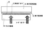
[第1実施形態]
本実施形態の素子の転写方法について、図1乃至図5を参照しながら説明する。先ず、図1に示すように、光透過性の第一基板であるサファイヤ基板10上に、発光ダイオード12がマトリクス状に配列されるように複数形成される。この発光ダイオード12は、窒化ガリウムなどの窒化物半導体系の材料によって構成される素子であり、一例として、活性層をクラッド層が挟んで構成されたダブルヘテロ構造を有する。発光ダイオード12は、サファイヤ基板10上で選択成長などによって窒化ガリウム結晶層などを積層させることで構成され、この図1の段階では所要の発光領域は形成されているが、最終的な配線は施されていない。マトリクス状に配列される発光ダイオード12は、個々の素子ごとに分離されてサファイヤ基板10上に配置されている。個々の素子ごとには、例えば、RIE(反応性イオンエッチング)などによって分離可能である。発光ダイオード12は略平板状であり、当該発光ダイオード12の活性層、クラッド層はサファイヤ基板10の主面と平行な面で延在される。
【0015】
これらの発光ダイオード12を一時保持するための素子保持基板14が用意され、その素子保持基板14のサファイヤ基板10に対向する面には素子保持層13が形成されている。素子保持基板14は所要の剛性を有した基板であり、半導体基板、石英ガラス基板、ガラス基板、プラスチック基板、金属基板などの種々の基板を用いることができる。この素子保持基板14は特にレーザー光などの光を透過させる必要がないので、光透過性の材料でなくとも良い。素子保持層13は一時的に発光ダイオード12の表面に接着して発光ダイオード12を保持する接着層である。素子保持層13は熱可塑性樹脂や熱硬化性樹脂などによって構成することができるが、特にシリコーン樹脂を用いることが好適である。シリコーン樹脂はエキシマレーザーやYAGレーザーの光を照射した場合でもアブレーションが発生せず、素子のみを剥離することができるので歩留まりを良くすることができる。
【0016】
素子保持層13が表面に形成された素子保持基板14がサファイヤ基板10の主面に対峙され、所要の圧力で複数の発光ダイオード12が素子保持層13の表面に圧着される。次に、図1に示すように、エキシマレーザーやYAGレーザーなどのレーザー光15を選択的に照射して、選択対象となる発光ダイオード12とサファイヤ基板10の界面にレーザーアブレーションを生じさせる。レーザーアブレーションとは、照射光を吸収した固定材料が光化学的または熱的に励起され、その表面や内部の原子または分子の結合が切断されて放出することをいい、主に固定材料の全部または一部が溶融、蒸発、気化などの相変化を生じる現象として現れる。このレーザーアブレーションによって、選択対象となる発光ダイオード12とサファイヤ基板10の間ではGaN系材料が金属のGaと窒素に分解してガスが発生する。このため発光ダイオード12は比較的簡単に剥離できる。照射されるレーザー光15としては、特に短波長域で高出力であることから、エキシマレーザーを用いることが好ましく、瞬時での処理が可能である。レーザー光15は選択対象となる発光ダイオード12に選択的に照射される。選択的な照射を行うために、所要の開口部を有するマスクを使用したり、照射、非照射を制御しながら走査するようにすることも可能である。
【0017】
図2はレーザーアブレーションにより、発光ダイオード12が選択的に剥離されたところを示す図であり、素子保持層13の表面13aに選択対象とされた発光ダイオード12が貼り付いて素子保持基板14側に保持される。
【0018】
次に、図3に示すように、発光ダイオード12が保持された素子保持基板14を基板ごと洗浄槽16内の洗浄液16fに浸漬し、発光ダイオード12のレーザーアブレーションによって剥がれた面に残存する金属等を洗浄によって除去する。この金属等は、主にレーザーアブレーションによって蒸発した窒素により生成された金属Gaを主体とするものである。洗浄液16fとしては、アルカリ系、酸系のどちらのエッチング液を用いても良く、この工程においても素子保持層13として特にシリコーン樹脂を用いた場合では、発光ダイオード12が素子保持層13の表面13aに貼りつけたまま洗浄を進めることができ、且つシリコーン樹脂は耐アルカリ、耐酸性であるため、侵食されることがなく、そのまま発光ダイオード12を保持できる。
【0019】
発光ダイオード12の洗浄の後、図4に示すように、主面上に接着剤層19が形成された第二基板18を用意する。この第二基板18は例えば石英ガラスなどの光透過性材料で構成され、また、接着剤層19としてはUV硬化型接着剤や、熱硬化型接着剤、熱可塑型接着剤などを用いることができる。この主面上に接着剤層19が形成された第二基板18を発光ダイオード12が保持された素子保持基板14上に合わせ、エネルギー光17の照射を行って、素子保持基板14上の発光ダイオード12を第二基板18に転写する。接着剤層19がUV硬化型接着剤の場合には、エネルギー光17として紫外線を照射することで接着剤層19を硬化することができ、接着剤層19の未硬化領域19yを発光ダイオード12に当接させた後に、紫外線を照射することで発光ダイオード12を着実に固着できる。接着剤層19が熱硬化型接着剤或いは熱可塑型接着剤の場合には、赤外線レーザー光を照射して硬化もしくは再溶融して接着できることになる。発光ダイオード12に対応する領域だけを硬化や再溶融して発光ダイオード12を接着するようにすることもでき、接着剤層19の全面を一括して硬化させたり再溶融させて発光ダイオード12を接着するようにしても良い。素子保持層13として特にシリコーン樹脂を用いた場合では、接着剤層19と素子保持層13が接触した場合でも、剥離性が優れており、容易に素子保持基板14を剥がすことができる。
【0020】
最後に、図5に示すように、素子保持層13ごと素子保持基板14が取り去られ、選択的な発光ダイオード12の転写が行われた第二基板18が得られることになる。
【0021】
上述の素子の転写方法においては、素子の剥離用のエネルギービームは素子と第一基板の界面に選択的に照射されるため、レーザーアブレーションによって素子と基板の界面での剥離が短時間で行われ、素子などへの損傷は生じない。素子と基板の界面はわざわざ形成したものではなく、素子を形成する過程で自然に形成される面であるために、剥離を目的とする剥離用の薄膜の形成は不要であって、工程数の増加は最小限に抑えることができる。また、発光ダイオード12は平板型であり、例えばシリコーン樹脂などより構成される素子保持層13に確実に貼りついて、位置ずれもなく転写される。従って、製造の歩留まりの低下を抑えて画像表示装置などを製造できることになる。
【0022】
[第2実施形態]
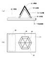
本実施形態の素子の転写方法について、先ず、図6に本実施形態で使用される素子の一例としての発光素子の構造を示す。この発光素子は尖頭部を有した素子構造を有する。図6の(a)が素子断面図であり、図6の(b)が平面図である。この発光素子はGaN系の発光ダイオードであり、たとえばサファイヤ基板上に結晶成長される素子である。このようなGaN系の発光ダイオードでは、基板を透過するレーザー照射によってレーザーアブレーションが生じ、GaNの窒素が気化する現象にともなってサファイヤ基板とGaN系の成長層の間の界面で膜剥がれが生じ、素子分離を容易なものにできる特徴を有している。
【0023】
まず、その構造については、GaN系半導体層からなる下地成長層31上に選択成長された六角錐形状のGaN層32が形成されている。なお、下地成長層31上には図示しない絶縁膜が存在し、六角錐形状のGaN層32はその絶縁膜を開口した部分にMOCVD法などによって形成される。このGaN層32は、成長時に使用されるサファイヤ基板の主面をC面とした場合にS面(1−101面)で覆われたピラミッド型の成長層であり、シリコンをドープさせた領域である。このGaN層32の傾斜したS面の部分はダブルへテロ構造のクラッドとして機能する。GaN層32の傾斜したS面を覆うように活性層であるInGaN層33が形成されており、その外側にマグネシュームドープのGaN層34が形成される。このマグネシュームドープのGaN層34もクラッドとして機能する。
【0024】
このような発光ダイオードには、p電極35とn電極36が形成されている。p電極35はマグネシュームドープのGaN層34上に形成されるNi/Pt/AuまたはNi(Pd)/Pt/Auなどの金属材料を蒸着して形成される。n電極36は前述の図示しない絶縁膜を開口した部分でTi/Al/Pt/Auなどの金属材料を蒸着して形成される。なお、下地成長層31の裏面側からn電極取り出しを行う場合は、n電極36の形成は下地成長層31の表面側には不要となる。
【0025】
このような構造のGaN系の発光ダイオードは、六角錐形状からなる尖頭部を備えた青色発光も可能な素子であって、特にレーザーアブレーションよって比較的簡単にサファイヤ基板から剥離することができ、レーザービームを選択的に照射することで選択的な剥離が実現される。なお、GaN系の発光ダイオードとしては、平板上や帯状に活性層が形成される構造であっても良く、上端部にC面が形成された角錐構造のものであっても良い。また、他の窒化物系発光素子や化合物半導体素子などであっても良い。
【0026】
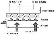
図7乃至図11を参照しながら説明する。図7に示すように、光透過性の第一基板であるサファイヤ基板40上に、六角錐形状の尖頭部42aを備えた発光ダイオード42がマトリクス状に配列されるように複数形成される。この発光ダイオード42は、窒化ガリウムなどの窒化物半導体系の材料によって構成される素子であり、一例として、活性層をクラッド層が挟んで構成されたダブルヘテロ構造を有する。発光ダイオード42は、主面をC面とするサファイヤ基板40上で選択成長などによって窒化ガリウム結晶層などを積層させることで構成され、この図7の段階では所要の発光領域は形成されているが、最終的な配線は施されていない。マトリクス状に配列される発光ダイオード42は、個々の素子ごとに分離されてサファイヤ基板40上に配置されている。個々の素子ごとには、例えば、RIE(反応性イオンエッチング)などによって分離可能である。発光ダイオード42の活性層、クラッド層は尖頭部42aの斜面と平行な面に延在される。
【0027】
これらの発光ダイオード42を一時保持するための素子保持基板44が用意され、その素子保持基板44のサファイヤ基板40に対向する面にはシリコーン樹脂層43が形成されている。素子保持基板44は所要の剛性を有した基板であり、半導体基板、石英ガラス基板、ガラス基板、プラスチック基板、金属基板などの種々の基板を用いることができる。この素子保持基板44は特にレーザー光などの光を透過させる必要がないので、光透過性の材料でなくとも良い。シリコーン樹脂層43は一時的に発光ダイオード42の表面に接着して発光ダイオード42を保持する接着層である。このシリコーン樹脂層43の表面には複数の凹部43bが発光ダイオード42の位置に形成されており、その各凹部43bの形状は発光ダイオード42の尖頭部42aを雄型とした場合の雌型の関係にあり、丁度尖頭部42aが嵌合する形状となっている。特に素子保持層としてシリコーン樹脂を用いることで、エキシマレーザーやYAGレーザーの光を照射した場合でもアブレーションが発生せず、素子のみを剥離することができ、歩留まりを良くすることができる。
【0028】
シリコーン樹脂層43が表面に形成された素子保持基板44がサファイヤ基板40の主面に対峙され、所要の圧力で複数の発光ダイオード42がシリコーン樹脂層43の表面に圧着される。次に、図7に示すように、エキシマレーザーやYAGレーザーなどのレーザー光45を選択的に照射して、選択対象となる発光ダイオード42とサファイヤ基板40の界面にレーザーアブレーションを生じさせる。レーザーアブレーションによって、選択対象となる発光ダイオード42とサファイヤ基板40の間ではGaN系材料が金属のGaと窒素に分解してガスが発生して、発光ダイオード42は比較的簡単に剥離できる。照射されるレーザー光45としては、特に短波長域で高出力であることから、エキシマレーザーを用いることが好ましく、瞬時での処理が可能である。レーザー光45は選択対象となる発光ダイオード42に選択的に照射される。選択的な照射を行うために、所要の開口部を有するマスクを使用したり、照射、非照射を制御しながら走査するようにすることも可能である。
【0029】
図8はレーザーアブレーションにより、発光ダイオード42が選択的に剥離されたところを示す図であり、シリコーン樹脂層43の表面に形成された凹部43bに選択対象とされた発光ダイオード42の尖頭部42aが嵌合して素子保持基板44側に着実に保持される。仮に、凹部43bを設けずに、平坦な表面で尖頭部42aを有する発光ダイオード42を保持しようとした場合では、尖頭部42aが倒れてしまって正確な位置決めができないなどの問題が生ずるが、本実施形態のように、凹部43bを設けることで発光ダイオード42が確実に保持されることになる。
【0030】
次に図9に示すように、発光ダイオード42が保持された素子保持基板44を基板ごと洗浄槽46内の洗浄液46fに浸漬し、発光ダイオード42のレーザーアブレーションによって剥がれた面に残存する金属等を洗浄によって除去する。この金属等は、主にレーザーアブレーションによって蒸発した窒素により生成された金属Gaを主体とするものである。洗浄液46fとしては、アルカリ系、酸系のどちらのエッチング液を用いても良く、この工程においてもシリコーン樹脂層43として特にシリコーン樹脂を用いた場合では、発光ダイオード42がシリコーン樹脂層43の表面43aに貼りつけたまま洗浄を進めることができ、且つシリコーン樹脂は耐アルカリ、耐酸性であるため、侵食されることがなく、そのまま発光ダイオード42を保持できる。
【0031】
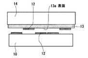
発光ダイオード42の洗浄の後、図10に示すように、主面上に接着剤層49が形成された第二基板48を用意する。この第二基板48は例えば石英ガラスなどの光透過性材料で構成され、また、接着剤層49としてはUV硬化型接着剤や、熱硬化型接着剤、熱可塑型接着剤などを用いることができる。この主面上に接着剤層49が形成された第二基板48を発光ダイオード42が保持された素子保持基板44上に合わせ、エネルギー光47の照射を行って、素子保持基板44上の発光ダイオード42を第二基板48に転写する。接着剤層49がUV硬化型接着剤の場合には、エネルギー光47として紫外線を照射することで接着剤層49を硬化することができ、接着剤層49の未硬化領域49yを発光ダイオード42に当接させた後に、紫外線を照射することで発光ダイオード42を着実に固着できる。接着剤層49が熱硬化型接着剤或いは熱可塑型接着剤の場合には、赤外線レーザー光を照射して硬化もしくは再溶融して接着できることになる。発光ダイオード42に対応する領域だけを硬化や再溶融して発光ダイオード42を接着するようにすることもでき、接着剤層49の全面を一括して硬化させたり再溶融させて発光ダイオード42を接着するようにしても良い。素子保持層としてシリコーン樹脂層43を形成していることから、接着剤層49とシリコーン樹脂層43が接触した場合でも、剥離性が優れており、容易に素子保持基板44を剥がすことができる。
【0032】
最後に、図11に示すように、凹部43bが形成されたシリコーン樹脂層43ごと素子保持基板44が取り去られ、選択的な発光ダイオード42の転写が行われた第二基板48が得られることになる。
【0033】
上述の素子の転写方法においては、素子の剥離用のエネルギービームは素子と第一基板の界面に選択的に照射されるため、レーザーアブレーションによって素子と基板の界面での剥離が短時間で行われ、素子などへの損傷は生じない。素子と基板の界面はわざわざ形成したものではなく、素子を形成する過程で自然に形成される面であるために、剥離を目的とする剥離用の薄膜の形成は不要であって、工程数の増加は最小限に抑えることができる。また、発光ダイオード42は尖頭部42aを有した構造とされているが、素子保持層であるシリコーン樹脂層43には該尖頭部42aと嵌合する凹部43bが形成されていることから、発光ダイオード42はシリコーン樹脂層43に確実に貼りついて、位置ずれもなく転写される。従って、製造の歩留まりの低下を抑えて画像表示装置などを製造できることになる。
【0034】
[第3の実施形態]
本実施形態は凹部を有するシリコーン樹脂層を形成した素子保持基板と、その形成方法についての実施形態である。図12乃至図14を参照しながらその形成方法について説明する。
【0035】
はじめに図12に示すように、サファイヤ基板50上に六角錐形状の尖頭部52aを備えた発光ダイオード52がマトリクス状に配列されるように複数形成される。この発光ダイオード52は、図6に示した発光ダイオードと同じ構成であり、窒化ガリウムなどの窒化物半導体系の材料によって構成される素子である。このマトリクス状に配列される発光ダイオード52は、個々の素子ごとに分離されてサファイヤ基板50上に配置されている。これら発光ダイオード52上には剥離層53が形成される。ここで剥離層53としてはテフロンやシリコーンなどの材料層が使用され、あるいは他の離型剤などを使用しても良い。このとき素子の形状を損なうことのないように、剥離層53の材料の粘度を低くする。このような低粘度への制御はキシレンなどの溶剤を使用することで可能である。
【0036】
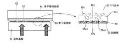
発光ダイオード52上を覆う剥離層53を硬化させた後、図13に示すように、素子保持基板55をサファイヤ基板50に対峙させ、これら素子保持基板55とサファイヤ基板50の間にボイドが入らないようにシリコーン樹脂を注入する。するとシリコーン樹脂は剥離層53が形成された発光ダイオード52の各尖頭部52aの間に回りこみ、発光ダイオード52の各尖頭部52aの形状を反映して硬化する。このシリコーン樹脂の硬化によって尖頭部52aと嵌合する形状の凹部54bを表面に形成するシリコーン樹脂層54が素子保持基板55上に形成される。
【0037】
続いて、型として使用した各発光ダイオード52をサファイヤ基板50ごと抜き取り、図14に示すように、尖頭部52aと嵌合する形状の凹部54bを表面に有するシリコーン樹脂層54を備えた素子保持基板55を完成する。サファイヤ基板50は、各発光ダイオード52上には剥離層53が形成されているために、容易に剥離することができる。
【0038】
このような尖頭部52aと嵌合する凹部54bを有するシリコーン樹脂層54を備えた素子保持基板55を用いることで、発光ダイオード52は尖頭部52a側が保持されて転写されるにもかかわらず、尖頭部52aと凹部54bが確実に嵌合するため、その位置ズレのない転写が実現される。また、シリコーン樹脂層は、レーザーアブレーションを生じないなどの利点があり、また、洗浄液に対しても耐アルカリ、耐酸性など点で取り扱いが容易である。
【0039】
[第4実施形態]
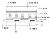
本実施形態の素子の転写方法について、図15乃至図19を参照しながら説明する。本実施形態は液晶表示素子に用いられる薄膜トランジスタ素子の転写の例である。先ず、図15に示すように、光透過性の第一基板であるガラスなどの透明基板61上に、薄膜トランジスタ(TFT)素子62がマトリクス状に配列されるように複数形成される。この時、薄膜トランジスタ素子62は液晶としての画素のピッチよりも大幅に狭いピッチで形成される。換言すると、転写時にピッチを広げられることから、薄膜トランジスタ素子62自体は高密度に形成することができる。
【0040】
この薄膜トランジスタ素子62の構造については、図15の右側の拡大図に示すように、再結晶化されたシリコンなどの半導体薄膜62a上にゲート絶縁膜を介してゲート電極層62gが形成されており、半導体薄膜62aは例えばシリコン酸化膜などからなる絶縁領域60の上に形成されている。半導体薄膜62aとゲート電極層62gは層間絶縁膜62iに被覆されており、半導体薄膜62aに形成されたソースドレイン領域62sd、62sd上の層間絶縁膜62iが開口され、配線電極62eが形成されている。絶縁領域60の下部には、レーザー照射によってレーザーアブレーションを生じさせる剥離膜59が形成される。
【0041】
この薄膜トランジスタ素子62は、後述するようにアクティブマトリクス型の液晶表示装置の各画素ごとに配列される素子であり、ガラスやプラスチックなどの透明材料からなる第二基板上に第一基板上から位置を離間するように形成される。この図1の段階では所要のトランジスタ領域は形成されているが、最終的な配線は施されていない。マトリクス状に配列される薄膜トランジスタ素子62は、個々の素子ごとに分離されて透明基板61上に配置されている。個々の薄膜トランジスタ素子62ごとには、例えば、RIE(反応性イオンエッチング)などによって分離可能である。
【0042】
これら薄膜トランジスタ素子62のを一時保持するための素子保持基板64が用意され、その素子保持基板64の透明基板61に対向する面には素子保持層63が形成されている。素子保持基板64は所要の剛性を有した基板であり、半導体基板、石英ガラス基板、ガラス基板、プラスチック基板、金属基板などの種々の基板を用いることができる。この素子保持基板64は特にレーザー光などの光を透過させる必要がないので、光透過性の材料でなくとも良い。素子保持層63は一時的に薄膜トランジスタ素子62の表面に接着して薄膜トランジスタ素子62を保持する接着層である。素子保持層63は熱可塑性樹脂や熱硬化性樹脂などによって構成することができるが、特にシリコーン樹脂を用いることが好適である。シリコーン樹脂はエキシマレーザーやYAGレーザーの光を照射した場合でもアブレーションが発生せず、素子のみを剥離することができるので歩留まりを良くすることができる。
【0043】
素子保持層63が表面に形成された素子保持基板64が透明基板61の主面に対峙され、所要の圧力で複数の薄膜トランジスタ素子62が素子保持層63の表面に圧着される。図15に示すように、エキシマレーザーやYAGレーザーなどのレーザー光を選択的に照射して、選択対象となる薄膜トランジスタ素子62と透明基板61の界面にレーザーアブレーションを生じさせる。このレーザーアブレーションによって、選択対象となる薄膜トランジスタ素子62と透明基板61の間では、薄膜トランジスタ素子62の底部に形成された剥離膜59にガスが発生する。このため薄膜トランジスタ素子62は比較的簡単に剥離できる。照射されるレーザー光としては、特に短波長域で高出力であることから、エキシマレーザーを用いることが好ましく、瞬時での処理が可能である。レーザー光は選択対象となる薄膜トランジスタ素子62に選択的に照射される。選択的な照射を行うために、所要の開口部を有するマスクを使用したり、照射、非照射を制御しながら走査するようにすることも可能である。剥離膜59としては、選択的に照射されるレーザーの特性に合わせた膜を選ぶことができ、たとえば非晶質シリコン薄膜や窒化膜などを用いることができる。
【0044】
図16はレーザーアブレーションにより、薄膜トランジスタ素子62が選択的に剥離されたところを示す図であり、素子保持層63の表面63aに選択対象とされた薄膜トランジスタ素子62が貼り付いて素子保持基板64側に保持される。このような選択的な剥離によって、第一基板上での素子ピッチを広げることができる。ここで選択対象とされる薄膜トランジスタ素子62の間隔は液晶表示装置の間隔と同じものとすることができ、高密度に形成した薄膜トランジスタ素子62を実装用の基板上で離間するようにできることになる。
【0045】
所要の洗浄等を行った後、図17に示すように、主面上に接着剤層69が形成された第二基板68を用意する。この第二基板68は例えば石英ガラスなどの光透過性材料で構成され、また、接着剤層69としてはUV硬化型接着剤や、熱硬化型接着剤、熱可塑型接着剤などを用いることができる。この主面上に接着剤層19が形成された第二基板68を薄膜トランジスタ素子62が保持された素子保持基板64上に合わせ、エネルギー光の照射を行って、素子保持基板64上の薄膜トランジスタ素子62を第二基板68に転写する。接着剤層69がUV硬化型接着剤の場合には、エネルギー光として紫外線を照射することで接着剤層69を硬化することができ、接着剤層69の未硬化領域69yを薄膜トランジスタ素子62に当接させた後に、紫外線を照射することで薄膜トランジスタ素子62を着実に固着できる。接着剤層69が熱硬化型接着剤或いは熱可塑型接着剤の場合には、赤外線レーザー光を照射して硬化もしくは再溶融して接着できることになる。薄膜トランジスタ素子62に対応する領域だけを硬化や再溶融して薄膜トランジスタ素子62を接着するようにすることもでき、接着剤層69の全面を一括して硬化させたり再溶融させて薄膜トランジスタ素子62を接着するようにしても良い。素子保持層63として特にシリコーン樹脂を用いた場合では、接着剤層69と素子保持層63が接触した場合でも、剥離性が優れており、容易に素子保持基板64を剥がすことができる。
【0046】
次に図18に示すように、素子保持層63ごと素子保持基板64が取り去られ、選択的な薄膜トランジスタ素子62の転写が行われた第二基板68が得られることになる。この段階で、液晶表示装置の画素ピッチに合わせた位置に各薄膜トランジスタ素子62が配列されていることになる。
【0047】
各薄膜トランジスタ素子62を画素ピッチに合わせて第二基板68上に転写した後、図19に示すように、層間絶縁膜70が各薄膜トランジスタ素子62上に形成され、その層間絶縁膜70に所要の窓部や配線部を形成した後、透明なITOなどによって構成される画素電極71が各画素ごとに形成され、その上に配向膜72が形成される。これと平行して、透明対向基板76上にITO膜などによる共通電極75が形成され、その上に配向膜74が形成される。最後に、所要の空隙を持って第二基板68上と透明対向基板76上を対向させ、第二基板68上と透明対向基板76の間に液晶73を注入して液晶表示装置を完成する。
【0048】
上述の素子の転写方法においては、素子の剥離用のエネルギービームは薄膜トランジスタ素子62と第一基板の界面に選択的に照射されるため、レーザーアブレーションによって素子と基板の界面での剥離が短時間で行われ、素子などへの損傷は生じない。また、各薄膜トランジスタ素子62は略平板型であり、例えばシリコーン樹脂などより構成される素子保持層63に確実に貼りついて、位置ずれもなく転写される。従って、製造の歩留まりの低下を抑えて液晶表示装置を製造できる。各薄膜トランジスタ素子62は第一基板上で高密度に形成されるため、大量生産による低コスト化が可能である。また、各薄膜トランジスタ素子62は画素ピッチに合わせて選択的に転写され、液晶表示装置の大画面化を容易に進めることができる。
【0049】
【発明の効果】
上述のように、本発明の素子の転写方法においては、素子の剥離用のエネルギービームは素子と第一基板の界面に選択的に照射されるため、レーザーアブレーションによって素子と基板の界面での剥離が短時間で行われ、素子などへの損傷は生じない。素子と基板の界面はわざわざ形成したものではなく、素子を形成する過程で自然に形成される面であるために、剥離を目的とする剥離用の薄膜の形成は不要であって、工程数の増加は最小限に抑えることができる。
【0050】
また、素子としての発光ダイオードが尖頭部を有した構造とされる場合では、素子保持層には該尖頭部と嵌合する凹部が形成されていることから、発光ダイオードは素子保持層に確実に貼りついて、位置ずれもなく転写される。従って、製造の歩留まりの低下を抑えて画像表示装置などを製造できることになる。また、素子としての発光ダイオードや液晶表示装置の薄膜トランジスタ素子が平板型である場合でも、同様に素子保持層に確実に貼りついて、位置ずれもなく転写される。
【0051】
また、本発明の素子保持基板と、その形成方法においては、素子の尖頭部に嵌合する凹部を形成した素子保持層を確実に形成することができ、前述の素子の転写方法に適用して、工程の増加を招かずに短時間での転写を可能とする。
【図面の簡単な説明】
【図1】本発明の第1実施形態の素子の転写方法におけるレーザー光の照射工程を示す工程断面図である。
【図2】本発明の第1実施形態の素子の転写方法における発光ダイオードの転写工程を示す工程断面図である。
【図3】本発明の第1実施形態の素子の転写方法における発光ダイオードの洗浄工程を示す工程断面図である。
【図4】本発明の第1実施形態の素子の転写方法における発光ダイオードの第二基板への転写工程を示す工程断面図である。
【図5】本発明の第1実施形態の素子の転写方法における発光ダイオードの第二基板への転写後の状態を示す工程断面図である。
【図6】本発明の実施形態の素子の転写方法に用いられる発光素子の例を示す図であって、(a)断面図と(b)平面図である。
【図7】本発明の第2実施形態の素子の転写方法におけるレーザー光の照射工程を示す工程断面図である。
【図8】本発明の第2実施形態の素子の転写方法における発光ダイオードの転写工程を示す工程断面図である。
【図9】本発明の第2実施形態の素子の転写方法における発光ダイオードの洗浄工程を示す工程断面図である。
【図10】本発明の第2実施形態の素子の転写方法における発光ダイオードの第二基板への転写工程を示す工程断面図である。
【図11】本発明の第2実施形態の素子の転写方法における発光ダイオードの第二基板への転写後の状態を示す工程断面図である。
【図12】本発明の第3実施形態の素子保持基板の製造方法における剥離層の形成工程を示す工程断面図である。
【図13】本発明の第3実施形態の素子保持基板の製造方法におけるシリコーン樹脂層の形成工程を示す工程断面図である。
【図14】本発明の第3実施形態の素子保持基板の製造方法における素子保持基板の剥離工程を示す工程断面図である。
【図15】本発明の第4実施形態の素子の転写方法におけるレーザー光の照射工程を示す工程断面図である。
【図16】本発明の第4実施形態の素子の転写方法における薄膜トランジスタ素子の剥離工程を示す工程断面図である。
【図17】本発明の第4実施形態の素子の転写方法における薄膜トランジスタ素子の接着工程を示す工程断面図である。
【図18】本発明の第4実施形態の素子の転写方法における薄膜トランジスタ素子の第二基板への転写工程を示す工程断面図である。
【図19】本発明の第4実施形態の素子の転写方法における液晶表示装置の組み立て工程を示す工程断面図である。
【符号の説明】
10、40 サファイヤ基板
12, 42 発光ダイオード
13 素子保持層
14、44 素子保持基板
15、45 レーザー光
16f、46f 洗浄液
18、48 第二基板
19、49 接着剤層
43 シリコーン樹脂層
42a 尖頭部
43b 凹部[0001]
BACKGROUND OF THE INVENTION
The present invention relates to an element transfer method for selectively peeling off a microfabricated element and transferring it onto another substrate, an element holding substrate forming method, and an element holding substrate.
[0002]
[Prior art]
Conventionally, when light emitting elements are arranged in a matrix and assembled into an image display device, the elements are formed on a substrate like a liquid crystal display (LCD) or a plasma display panel (PDP). Alternatively, a single LED package such as a light emitting diode display (LED display) is arranged. In conventional image display devices such as LCDs and PDPs, the element and pixel pitches and the manufacturing process thereof cannot be separated, so that each element is spaced by the pixel pitch of the image display device from the beginning of the manufacturing process. It is usually done.
[0003]
In addition to a light emitting element, there is a technique for densely forming a semiconductor thin film element or a semiconductor element once on a substrate and transferring it to another substrate. For example, transfer of a thin film device described in JP-A-11-26733 In the method, a substrate used at the time of manufacturing a thin film device as a liquid crystal control element is different from a substrate used at the time of mounting a product, and the thin film device is transferred to the substrate used at the time of mounting. As another transfer technique, for example, there is a transfer method described in Japanese Patent Application Laid-Open No. 7-254690, in which a film that generates microbubbles is formed at a boundary portion with an element portion (semiconductor plate) on a substrate, and laser There is also known an example in which microbubbles are generated by beam irradiation and the element portion (semiconductor plate) is transferred to the support side. Further, in the technique described in JP-A-11-142878, the thin film transistor constituting the liquid crystal display portion on the first substrate is entirely transferred onto the second substrate, and then selectively from the second substrate. A technique for transferring to a third substrate corresponding to the pixel pitch is disclosed.
[0004]
[Problems to be solved by the invention]
However, the transfer technique as described above has the following problems. First, in the thin film device transfer method described in Japanese Patent Application Laid-Open No. 11-26733, the hot melt adhesive layer of the second separation layer is ablated by irradiation with laser light, and gas is generated at that time. The processing becomes a problem in the process. Further, the adhesive layer itself remains when the element is transferred to the secondary transfer body, and it is necessary to remove the hot-melt adhesive layer using xylene or the like. In order to cure the epoxy resin as the adhesive layer and adhere it to the next transfer body, a long curing time for curing the epoxy resin is required. Further, in order to peel a thin film device such as a thin film transistor from the entire substrate, it is necessary to previously form amorphous silicon on the entire surface of the substrate, and laser irradiation must be performed on the entire surface of the substrate.
[0005]
In the transfer method described in JP-A-7-254690, since the laser irradiation is transmitted through the support, the support is limited to one that transmits the laser. In addition, this publication describes that sufficient binding energy is provided between the semiconductor plate and the support and adheres to the support, but laser absorption is performed between the semiconductor plate and the support. As a result, bubbles may be generated by ablation and the semiconductor element may be destroyed, resulting in a decrease in yield.
[0006]
Further, in the technique described in JP-A-11-142878, UV light is selectively irradiated to a portion of a thin film transistor element to be transferred, and a UV release resin formed between the thin film transistor element and a transfer source substrate is used. The adhesive force is reduced. However, it takes time for the adhesive strength of the UV release resin to decrease due to the irradiation of ultraviolet rays, leading to a decrease in throughput in the process, and when the adhesive strength cannot be sufficiently reduced, the transfer yield also decreases. Will end up.
[0007]
Accordingly, the present invention provides an element transfer method and an element holding substrate manufacturing method capable of transferring a microfabricated element in a short time without increasing the number of processes and reducing the transfer yield. It is an object to provide a method and an element holding substrate.
[0008]
[Means for Solving the Problems]
In order to solve the above technical problem, the element transfer method of the present invention includes a first substrate and,this Formed on the first substrateWith pointed head elementWhen On the interface, While passing through the first substrateEnergy beam Selectively irradiating and selectively peeling the element;, Select Selectively stripped elementsThe element formed on the surface of the element holding substrate is formed with a concave portion that fits the pointed head. A step of transferring to the child holding layer;, Raw And transferring the element transferred to the child holding layer to the second substrate.
[0009]
In the element transfer method described above, the energy beam for element separation is selectively applied to the interface between the element and the first substrate. Therefore, there is no energy in unnecessary portions, and separation at the interface between the element and the substrate occurs. Since the process is performed in a short time and the interface between the element and the substrate is not intentionally formed, it is a surface that is formed naturally during the process of forming the element, so the increase in the number of processes for peeling is minimized. be able to.
[0010]
In the present invention, an element made of a material that causes ablation by irradiation with an energy beam can be used as the element, for example, a semiconductor light emitting element made of a nitride semiconductor material can be used. A semiconductor light emitting device made of this nitride semiconductor material can be produced by crystal growth on a sapphire substrate. Since the sapphire substrate transmits a required energy beam, an energy beam that causes peeling is applied to the sapphire substrate. It can be led to the interface between the substrate and the semiconductor light emitting device.
[0011]
Further, the element holding substrate forming method of the present invention provides a substrate on which an element having a pointed head is formed.And a process of On the element holding substrate, Face the substrate so that the tip of the element is not in contact with the element holding substrate, and between the substrate and the element holding substrate Uncured silicone resin layerThe step of injecting, the step of curing the silicone resin layer, and the element having a pointed head from the cured silicone resin layer are separated from the substrate, Ricone resin layerOn the surface of the tip Concave part shaped to fit the headShape CompleteAnd having a process It is characterized by that.
[0012]
Since the concave portion is formed on the surface of the silicone resin layer so as to be fitted to the pointed portion of the element, the element having the pointed portion can be reliably held so as not to cause a positional deviation during holding. . Furthermore, the silicone resin layer has adhesiveness on the surface itself, and can reliably hold the element from the fitting between the pointed head and the recess.
[0013]
BEST MODE FOR CARRYING OUT THE INVENTION
Hereinafter, embodiments of the present invention will be described in detail with reference to the drawings. The first embodiment is an example of a method for selectively transferring a planar light emitting diode, the second embodiment is an example of a method for selectively transferring a light emitting diode having a pointed head, and The third embodiment is an example of a method for manufacturing an element holding substrate using a silicone resin layer.
[0014]
[First embodiment]
The element transfer method of this embodiment will be described with reference to FIGS. First, as shown in FIG. 1, a plurality of
[0015]
An
[0016]
The
[0017]
FIG. 2 is a view showing a state where the
[0018]
Next, as shown in FIG. 3, the
[0019]
After cleaning the
[0020]
Finally, as shown in FIG. 5, the
[0021]
In the above-described element transfer method, the energy beam for element separation is selectively applied to the interface between the element and the first substrate, and therefore, the separation at the element-substrate interface is performed in a short time by laser ablation. There is no damage to the elements. Since the interface between the element and the substrate is not purposely formed, but is a surface that is naturally formed in the process of forming the element, it is not necessary to form a thin film for peeling for the purpose of peeling. The increase can be minimized. Further, the
[0022]
[Second Embodiment]
Regarding the element transfer method of the present embodiment, first, FIG. 6 shows a structure of a light emitting element as an example of an element used in the present embodiment. This light emitting element has an element structure having a pointed head. FIG. 6A is an element cross-sectional view, and FIG. 6B is a plan view. This light-emitting element is a GaN-based light-emitting diode, for example, an element that is crystal-grown on a sapphire substrate. In such a GaN-based light emitting diode, laser ablation occurs due to laser irradiation that passes through the substrate, and film peeling occurs at the interface between the sapphire substrate and the GaN-based growth layer due to the phenomenon of nitrogen vaporization of GaN, It has a feature that element isolation can be made easy.
[0023]
First, with respect to the structure, a hexagonal pyramid-shaped
[0024]
In such a light emitting diode, a p-
[0025]
A GaN-based light emitting diode having such a structure is an element capable of emitting blue light with a pointed head having a hexagonal pyramid shape, and can be peeled off from a sapphire substrate relatively easily by laser ablation, Selective peeling is realized by selectively irradiating a laser beam. The GaN-based light emitting diode may have a structure in which an active layer is formed on a flat plate or in a strip shape, or may have a pyramid structure in which a C surface is formed at the upper end. Further, other nitride-based light emitting elements, compound semiconductor elements, and the like may be used.
[0026]
This will be described with reference to FIGS. As shown in FIG. 7, a plurality of light-emitting
[0027]
An
[0028]
The
[0029]
FIG. 8 is a view showing a state where the
[0030]
Next, as shown in FIG. 9, the
[0031]
After cleaning the
[0032]
Finally, figure11 As shown in FIG. 5, the
[0033]
In the above-described element transfer method, the energy beam for element separation is selectively applied to the interface between the element and the first substrate, and therefore, the separation at the element-substrate interface is performed in a short time by laser ablation. There is no damage to the elements. Since the interface between the element and the substrate is not purposely formed, but is a surface that is naturally formed in the process of forming the element, it is not necessary to form a thin film for peeling for the purpose of peeling. The increase can be minimized. The
[0034]
[Third embodiment]
The present embodiment is an embodiment of an element holding substrate on which a silicone resin layer having a recess is formed, and a method for forming the same. The formation method will be described with reference to FIGS.
[0035]
First, as shown in FIG. 12, a plurality of
[0036]
After the
[0037]
Subsequently, each light-emitting
[0038]
By using the element holding substrate 55 provided with the
[0039]
[Fourth embodiment]
The element transfer method of the present embodiment will be described with reference to FIGS. This embodiment is an example of transfer of a thin film transistor element used for a liquid crystal display element. First, as shown in FIG. 15, a plurality of thin film transistor (TFT)
[0040]
As for the structure of this thin
[0041]
As will be described later, the thin
[0042]
An
[0043]
The
[0044]
FIG. 16 is a view showing a state where the thin
[0045]
After performing necessary cleaning or the like, as shown in FIG. 17, a
[0046]
Next, as shown in FIG. 18, the
[0047]
After the thin
[0048]
In the element transfer method described above, the energy beam for element separation is selectively applied to the interface between the thin
[0049]
【The invention's effect】
As described above, in the element transfer method of the present invention, the energy beam for element peeling is selectively irradiated to the interface between the element and the first substrate, and therefore, peeling at the interface between the element and the substrate by laser ablation. Is performed in a short time, and no damage to the element or the like occurs. Since the interface between the element and the substrate is not purposely formed, but is a surface that is naturally formed in the process of forming the element, it is not necessary to form a thin film for peeling for the purpose of peeling. The increase can be minimized.
[0050]
Further, in the case where the light emitting diode as an element has a structure having a pointed head, the element holding layer is formed with a concave portion that fits the pointed head, so that the light emitting diode is formed in the element holding layer. It sticks securely and is transferred without displacement. Therefore, it is possible to manufacture an image display device or the like while suppressing a decrease in manufacturing yield. Further, even when the light emitting diode as the element or the thin film transistor element of the liquid crystal display device is a flat plate type, the light emitting diode is similarly securely attached to the element holding layer and transferred without misalignment.
[0051]
Further, in the element holding substrate of the present invention and the method for forming the same, the element holding layer in which the concave portion fitted to the pointed portion of the element can be reliably formed, which is applied to the above-described element transfer method. Thus, the transfer can be performed in a short time without increasing the number of steps.
[Brief description of the drawings]
FIG. 1 is a process cross-sectional view illustrating a laser light irradiation process in an element transfer method according to a first embodiment of the present invention.
FIG. 2 is a process sectional view showing a light emitting diode transfer process in the element transfer method according to the first embodiment of the present invention;
FIG. 3 is a process cross-sectional view illustrating a light-emitting diode cleaning process in the element transfer method according to the first embodiment of the present invention;
FIG. 4 is a process cross-sectional view illustrating a process of transferring a light emitting diode to a second substrate in the element transfer method according to the first embodiment of the present invention;
FIG. 5 is a process sectional view showing a state after the light-emitting diode is transferred to the second substrate in the element transfer method according to the first embodiment of the present invention;
6A and 6B are diagrams showing an example of a light-emitting element used in the element transfer method according to the embodiment of the present invention, and are (a) a sectional view and (b) a plan view.
FIG. 7 is a process sectional view showing a laser beam irradiation process in the element transfer method according to the second embodiment of the present invention;
FIG. 8 is a process sectional view showing a light emitting diode transfer process in the element transfer method of the second embodiment of the present invention;
FIG. 9 is a process cross-sectional view illustrating a light-emitting diode cleaning process in the element transfer method according to the second embodiment of the present invention;
FIG. 10 is a process cross-sectional view illustrating a process of transferring a light emitting diode to a second substrate in the element transfer method according to the second embodiment of the present invention.
FIG. 11 is a process cross-sectional view illustrating a state after the light-emitting diode is transferred to the second substrate in the element transfer method according to the second embodiment of the present invention.
FIG. 12 is a process cross-sectional view illustrating a process for forming a release layer in the method for manufacturing an element holding substrate according to the third embodiment of the present invention.
FIG. 13 is a process cross-sectional view illustrating a process of forming a silicone resin layer in the method for manufacturing an element holding substrate according to the third embodiment of the present invention.
FIG. 14 is a process cross-sectional view illustrating an element holding substrate peeling step in the element holding substrate manufacturing method of the third embodiment of the present invention.
FIG. 15 is a process sectional view showing a laser beam irradiation process in the element transfer method according to the fourth embodiment of the present invention;
FIG. 16 is a process sectional view showing a thin film transistor element peeling step in the element transfer method according to the fourth embodiment of the present invention;
FIG. 17 is a process cross-sectional view illustrating an adhesion process of a thin film transistor element in an element transfer method according to a fourth embodiment of the present invention.
FIG. 18 is a process sectional view showing a process of transferring a thin film transistor element to a second substrate in the element transfer method of the fourth embodiment of the invention.
FIG. 19 is a process cross-sectional view illustrating an assembly process of a liquid crystal display device in an element transfer method according to a fourth embodiment of the present invention.
[Explanation of symbols]
10, 40 Sapphire substrate
12, 42 Light emitting diode
13 Device retention layer
14, 44 Element holding substrate
15, 45 Laser light
16f, 46f Cleaning fluid
18, 48 Second board
19, 49 Adhesive layer
43 Silicone resin layer
42a pointed head
43b recess
Claims (11)
Translated fromJapanese前記選択的に剥離された素子を、素子保持基板上の、前記尖頭部と嵌合する形状の凹部を表面に形成して成る素子保持層に転写する工程と、
前記素子保持層に転写された前記素子を第二基板に転写する工程とを有する
素子の転写方法。A firstsubstrate, the interfacebetween the elementhaving a head cusp formed on said firstsubstrate, the step of selectively separating the the element is selectively irradiated withan energy beam while transmittingthe first substrate When,
A step of transferring the selectively exfoliatedelements, on the element holding substrate, theelement holding layerobtained by forming a recess in a surface shaped to mate with the peak portion,
And transferring the element transferred to the element holding layer to a second substrate.
Transfer method of theelement.
素子保持基板上に、前記基板を前記素子の尖頭部が前記素子保持基板に接触しない状態で対峙させて、前記基板と前記素子保持基板との間に未硬化のシリコーン樹脂層を注入する工程と、
前記シリコーン樹脂層を硬化する工程と、
硬化後の前記シリコーン樹脂層から前記尖頭部を有する素子を前記基板ごと分離して、前記シリコーン樹脂層の表面に、前記尖頭部と嵌合する形状の凹部を形成する工程とを有する
素子保持基板の形成方法。Preparing a substrate on which an element having a pointed head is formed;
A process ofinjecting an uncured silicone resin layerbetween the substrate and the element holding substrate on the element holding substrate so that the substrate faces the tip of the element without contacting the element holding substrateWhen,
Curing the silicone resin layer;
The element having the peak portion from the silicone resin layer after curing were separated by the substrate,the surface of the silicone resinlayer,and a step that formsthe shape of the recess shaped to fit with the cusp
The method of forming theelement holding substrate.
素子保持基板。A substrate having a silicone resin layer formed on the substrate,that is a recess configured to fit the peak of the element to be held on the surface of the silicone resin layer
Element holding substrate.
Priority Applications (3)
| Application Number | Priority Date | Filing Date | Title |
|---|---|---|---|
| JP2000380944AJP4461616B2 (en) | 2000-12-14 | 2000-12-14 | Element transfer method, element holding substrate forming method, and element holding substrate |
| US10/024,690US6939729B2 (en) | 2000-12-14 | 2001-12-14 | Method of transferring a device, a method of producing a device holding substrate, and a device holding substrate |
| US11/059,865US6969624B2 (en) | 2000-12-14 | 2005-02-17 | Method of transferring a device, a method of producing a device holding substrate, and a device holding substrate |
Applications Claiming Priority (1)
| Application Number | Priority Date | Filing Date | Title |
|---|---|---|---|
| JP2000380944AJP4461616B2 (en) | 2000-12-14 | 2000-12-14 | Element transfer method, element holding substrate forming method, and element holding substrate |
Publications (2)
| Publication Number | Publication Date |
|---|---|
| JP2002185039A JP2002185039A (en) | 2002-06-28 |
| JP4461616B2true JP4461616B2 (en) | 2010-05-12 |
Family
ID=18849046
Family Applications (1)
| Application Number | Title | Priority Date | Filing Date |
|---|---|---|---|
| JP2000380944AExpired - LifetimeJP4461616B2 (en) | 2000-12-14 | 2000-12-14 | Element transfer method, element holding substrate forming method, and element holding substrate |
Country Status (2)
| Country | Link |
|---|---|
| US (2) | US6939729B2 (en) |
| JP (1) | JP4461616B2 (en) |
Families Citing this family (111)
| Publication number | Priority date | Publication date | Assignee | Title |
|---|---|---|---|---|
| JP4649745B2 (en)* | 2001-02-01 | 2011-03-16 | ソニー株式会社 | Light-emitting element transfer method |
| JP4691793B2 (en)* | 2001-02-06 | 2011-06-01 | ソニー株式会社 | Method for manufacturing element array type device |
| US6562701B2 (en)* | 2001-03-23 | 2003-05-13 | Matsushita Electric Industrial Co., Ltd. | Method of manufacturing nitride semiconductor substrate |
| US6872635B2 (en)* | 2001-04-11 | 2005-03-29 | Sony Corporation | Device transferring method, and device arraying method and image display unit fabricating method using the same |
| JP2003045901A (en)* | 2001-08-01 | 2003-02-14 | Sony Corp | Method for transferring element and method for arraying element using the same, and method for manufacturing image display unit |
| JP2003077940A (en)* | 2001-09-06 | 2003-03-14 | Sony Corp | Device transfer method, device array method using the same, and image display device manufacturing method |
| JP4055405B2 (en)* | 2001-12-03 | 2008-03-05 | ソニー株式会社 | Electronic component and manufacturing method thereof |
| JP2003282478A (en)* | 2002-01-17 | 2003-10-03 | Sony Corp | Alloying method, wiring forming method, display element forming method, image display device manufacturing method |
| US20040140474A1 (en)* | 2002-06-25 | 2004-07-22 | Matsushita Electric Industrial Co., Ltd. | Semiconductor light-emitting device, method for fabricating the same and method for bonding the same |
| TWI300589B (en)* | 2002-07-17 | 2008-09-01 | Univ Nat Chiao Tung | |
| AU2003284410A1 (en)* | 2002-11-19 | 2004-06-15 | Ishikawa Seisakusho, Ltd. | Pixel control element selection transfer method, pixel control element mounting device used for pixel control element selection transfer method, wiring formation method after pixel control element transfer, and planar display substrate |
| KR100495215B1 (en) | 2002-12-27 | 2005-06-14 | 삼성전기주식회사 | VERTICAL GaN LIGHT EMITTING DIODE AND METHOD OF PRODUCING THE SAME |
| US20040259279A1 (en)* | 2003-04-15 | 2004-12-23 | Erchak Alexei A. | Light emitting device methods |
| US7344903B2 (en)* | 2003-09-17 | 2008-03-18 | Luminus Devices, Inc. | Light emitting device processes |
| US7341880B2 (en)* | 2003-09-17 | 2008-03-11 | Luminus Devices, Inc. | Light emitting device processes |
| DE10361521A1 (en)* | 2003-12-03 | 2005-07-07 | Pac Tech - Packaging Technologies Gmbh | Method of alternate contacting of two wafers especially a semiconductor and a functional component wafer uses selected laser wavelength to fuse contact metallization only |
| KR101149683B1 (en)* | 2003-12-03 | 2012-05-24 | 파크 테크-파카징 테크놀로지이스 게엠베하 | Method and device for the alternating contacting of two wafers |
| WO2005091390A1 (en)* | 2004-03-18 | 2005-09-29 | Showa Denko K.K. | Group iii nitride semiconductor light-emitting device and producing method thereof |
| JP4622720B2 (en)* | 2004-07-21 | 2011-02-02 | 日亜化学工業株式会社 | Method for manufacturing nitride semiconductor wafer or nitride semiconductor device |
| US20090023239A1 (en)* | 2004-07-22 | 2009-01-22 | Luminus Devices, Inc. | Light emitting device processes |
| JP2006196712A (en)* | 2005-01-13 | 2006-07-27 | Toshiba Corp | Thin film element manufacturing method |
| US7989958B2 (en)* | 2005-06-14 | 2011-08-02 | Cufer Assett Ltd. L.L.C. | Patterned contact |
| DE102005055293A1 (en)* | 2005-08-05 | 2007-02-15 | Osram Opto Semiconductors Gmbh | Method for producing semiconductor chips and thin-film semiconductor chip |
| US7622245B2 (en)* | 2005-10-11 | 2009-11-24 | Home Box Office, Inc. | Manufacturing data-storage media using light-curable material |
| KR101230310B1 (en)* | 2006-02-02 | 2013-02-06 | 삼성디스플레이 주식회사 | Adhesive and method for manufacturing display device using the same |
| DE102007004303A1 (en) | 2006-08-04 | 2008-02-07 | Osram Opto Semiconductors Gmbh | Thin-film semiconductor device and device composite |
| KR101588019B1 (en)* | 2006-09-20 | 2016-02-12 | 더 보오드 오브 트러스티스 오브 더 유니버시티 오브 일리노이즈 | Release strategies for making transferable semiconductor structures, devices and device components |
| TWI420691B (en)* | 2006-11-20 | 2013-12-21 | 尼康股份有限公司 | LED device and method of manufacturing same |
| DE102007004304A1 (en) | 2007-01-29 | 2008-07-31 | Osram Opto Semiconductors Gmbh | Thin-film light emitting diode chip, has layer stack made of primary radiation surfaces lying opposite to each other so that thin-film light emitting diode chip has two primary radiation directions |
| US8110425B2 (en) | 2007-03-20 | 2012-02-07 | Luminus Devices, Inc. | Laser liftoff structure and related methods |
| DE102007043877A1 (en)* | 2007-06-29 | 2009-01-08 | Osram Opto Semiconductors Gmbh | Process for the production of optoelectronic components and optoelectronic component |
| US8201325B2 (en)* | 2007-11-22 | 2012-06-19 | International Business Machines Corporation | Method for producing an integrated device |
| JP4640498B2 (en)* | 2008-12-11 | 2011-03-02 | ソニー株式会社 | Element transfer method, element arrangement substrate, device and manufacturing method thereof |
| JP2010177390A (en)* | 2009-01-29 | 2010-08-12 | Sony Corp | Method of transferring device and method of manufacturing display apparatus |
| KR101077789B1 (en)* | 2009-08-07 | 2011-10-28 | 한국과학기술원 | LED display manufacturing method and LED display manufactured thereby |
| KR101221871B1 (en)* | 2009-12-07 | 2013-01-15 | 한국전자통신연구원 | method for manufacturing semiconductor device |
| WO2011126726A1 (en) | 2010-03-29 | 2011-10-13 | Semprius, Inc. | Electrically bonded arrays of transfer printed active components |
| US9496155B2 (en)* | 2010-03-29 | 2016-11-15 | Semprius, Inc. | Methods of selectively transferring active components |
| US9161448B2 (en) | 2010-03-29 | 2015-10-13 | Semprius, Inc. | Laser assisted transfer welding process |
| JP2012064710A (en)* | 2010-09-15 | 2012-03-29 | Asahi Glass Co Ltd | Manufacturing method of semiconductor element |
| US9899329B2 (en) | 2010-11-23 | 2018-02-20 | X-Celeprint Limited | Interconnection structures and methods for transfer-printed integrated circuit elements with improved interconnection alignment tolerance |
| US9765934B2 (en) | 2011-05-16 | 2017-09-19 | The Board Of Trustees Of The University Of Illinois | Thermally managed LED arrays assembled by printing |
| DE102011103589B4 (en)* | 2011-05-30 | 2024-08-08 | Hegla Boraident Gmbh & Co. Kg | Method for removing a layer on a carrier substrate |
| US8889485B2 (en) | 2011-06-08 | 2014-11-18 | Semprius, Inc. | Methods for surface attachment of flipped active componenets |
| US9412727B2 (en) | 2011-09-20 | 2016-08-09 | Semprius, Inc. | Printing transferable components using microstructured elastomeric surfaces with pressure modulated reversible adhesion |
| WO2014037829A1 (en)* | 2012-09-05 | 2014-03-13 | Koninklijke Philips N.V. | Laser de-bond of carrier wafer from device wafer |
| JP2015157348A (en)* | 2014-01-21 | 2015-09-03 | ソニー株式会社 | Holding head, feeding apparatus, feeding method, implementing apparatus, implementing method, and electronic device |
| US9929053B2 (en) | 2014-06-18 | 2018-03-27 | X-Celeprint Limited | Systems and methods for controlling release of transferable semiconductor structures |
| US9444015B2 (en) | 2014-06-18 | 2016-09-13 | X-Celeprint Limited | Micro assembled LED displays and lighting elements |
| US9358775B2 (en) | 2014-07-20 | 2016-06-07 | X-Celeprint Limited | Apparatus and methods for micro-transfer-printing |
| US9209142B1 (en)* | 2014-09-05 | 2015-12-08 | Skorpios Technologies, Inc. | Semiconductor bonding with compliant resin and utilizing hydrogen implantation for transfer-wafer removal |
| US9799719B2 (en) | 2014-09-25 | 2017-10-24 | X-Celeprint Limited | Active-matrix touchscreen |
| US9991163B2 (en) | 2014-09-25 | 2018-06-05 | X-Celeprint Limited | Small-aperture-ratio display with electrical component |
| US9871345B2 (en) | 2015-06-09 | 2018-01-16 | X-Celeprint Limited | Crystalline color-conversion device |
| US11061276B2 (en) | 2015-06-18 | 2021-07-13 | X Display Company Technology Limited | Laser array display |
| US10133426B2 (en) | 2015-06-18 | 2018-11-20 | X-Celeprint Limited | Display with micro-LED front light |
| US9704821B2 (en) | 2015-08-11 | 2017-07-11 | X-Celeprint Limited | Stamp with structured posts |
| US11495560B2 (en)* | 2015-08-10 | 2022-11-08 | X Display Company Technology Limited | Chiplets with connection posts |
| US10468363B2 (en)* | 2015-08-10 | 2019-11-05 | X-Celeprint Limited | Chiplets with connection posts |
| US10380930B2 (en) | 2015-08-24 | 2019-08-13 | X-Celeprint Limited | Heterogeneous light emitter display system |
| US10230048B2 (en) | 2015-09-29 | 2019-03-12 | X-Celeprint Limited | OLEDs for micro transfer printing |
| EP3262694B1 (en)* | 2015-10-20 | 2019-08-21 | Goertek. Inc | Method for transferring micro-leds and method for manufacturing micro-led device |
| US10066819B2 (en) | 2015-12-09 | 2018-09-04 | X-Celeprint Limited | Micro-light-emitting diode backlight system |
| US9786646B2 (en) | 2015-12-23 | 2017-10-10 | X-Celeprint Limited | Matrix addressed device repair |
| TWI710061B (en) | 2016-02-25 | 2020-11-11 | 愛爾蘭商艾克斯展示公司技術有限公司 | Efficiently micro-transfer printing micro-scale devices onto large-format substrates |
| US10193025B2 (en) | 2016-02-29 | 2019-01-29 | X-Celeprint Limited | Inorganic LED pixel structure |
| US10153256B2 (en) | 2016-03-03 | 2018-12-11 | X-Celeprint Limited | Micro-transfer printable electronic component |
| US10153257B2 (en) | 2016-03-03 | 2018-12-11 | X-Celeprint Limited | Micro-printed display |
| US10103069B2 (en) | 2016-04-01 | 2018-10-16 | X-Celeprint Limited | Pressure-activated electrical interconnection by micro-transfer printing |
| US10008483B2 (en) | 2016-04-05 | 2018-06-26 | X-Celeprint Limited | Micro-transfer printed LED and color filter structure |
| US10199546B2 (en) | 2016-04-05 | 2019-02-05 | X-Celeprint Limited | Color-filter device |
| US9997501B2 (en) | 2016-06-01 | 2018-06-12 | X-Celeprint Limited | Micro-transfer-printed light-emitting diode device |
| US11137641B2 (en) | 2016-06-10 | 2021-10-05 | X Display Company Technology Limited | LED structure with polarized light emission |
| CN106099641A (en)* | 2016-07-08 | 2016-11-09 | 燕山大学 | A kind of preparation method of semiconductor laser |
| US10222698B2 (en) | 2016-07-28 | 2019-03-05 | X-Celeprint Limited | Chiplets with wicking posts |
| US11064609B2 (en) | 2016-08-04 | 2021-07-13 | X Display Company Technology Limited | Printable 3D electronic structure |
| US9980341B2 (en) | 2016-09-22 | 2018-05-22 | X-Celeprint Limited | Multi-LED components |
| US10782002B2 (en) | 2016-10-28 | 2020-09-22 | X Display Company Technology Limited | LED optical components |
| US10347168B2 (en) | 2016-11-10 | 2019-07-09 | X-Celeprint Limited | Spatially dithered high-resolution |
| US10395966B2 (en) | 2016-11-15 | 2019-08-27 | X-Celeprint Limited | Micro-transfer-printable flip-chip structures and methods |
| EP3542394B1 (en) | 2016-11-15 | 2025-09-24 | X Display Company Technology Limited | Micro-transfer-printable flip-chip structures and manufacturing methods thereof |
| US10600671B2 (en) | 2016-11-15 | 2020-03-24 | X-Celeprint Limited | Micro-transfer-printable flip-chip structures and methods |
| US10438859B2 (en) | 2016-12-19 | 2019-10-08 | X-Celeprint Limited | Transfer printed device repair |
| US10297502B2 (en) | 2016-12-19 | 2019-05-21 | X-Celeprint Limited | Isolation structure for micro-transfer-printable devices |
| US10396137B2 (en) | 2017-03-10 | 2019-08-27 | X-Celeprint Limited | Testing transfer-print micro-devices on wafer |
| US11024608B2 (en) | 2017-03-28 | 2021-06-01 | X Display Company Technology Limited | Structures and methods for electrical connection of micro-devices and substrates |
| US10353243B2 (en)* | 2017-08-01 | 2019-07-16 | Innolux Corporation | Display device |
| US10297585B1 (en) | 2017-12-21 | 2019-05-21 | X-Celeprint Limited | Multi-resolution compound micro-devices |
| US10446729B1 (en)* | 2018-03-22 | 2019-10-15 | Innolux Corporation | Display device having an electronic device disposed on a first pad and a second pad |
| US10984708B1 (en)* | 2018-03-30 | 2021-04-20 | Facebook Technologies, Llc | Manufacture LED displays using temporary carriers |
| US10431519B1 (en)* | 2018-05-03 | 2019-10-01 | Micron Technology, Inc. | Carrier removal by use of multilayer foil |
| US10505079B2 (en) | 2018-05-09 | 2019-12-10 | X-Celeprint Limited | Flexible devices and methods using laser lift-off |
| US10796971B2 (en) | 2018-08-13 | 2020-10-06 | X Display Company Technology Limited | Pressure-activated electrical interconnection with additive repair |
| KR102590229B1 (en) | 2018-10-15 | 2023-10-17 | 삼성전자주식회사 | Light emitting diode, manufacturing method of light emitting diode |
| US10796938B2 (en) | 2018-10-17 | 2020-10-06 | X Display Company Technology Limited | Micro-transfer printing with selective component removal |
| US10573544B1 (en) | 2018-10-17 | 2020-02-25 | X-Celeprint Limited | Micro-transfer printing with selective component removal |
| US11483937B2 (en) | 2018-12-28 | 2022-10-25 | X Display Company Technology Limited | Methods of making printed structures |
| US10748793B1 (en) | 2019-02-13 | 2020-08-18 | X Display Company Technology Limited | Printing component arrays with different orientations |
| US11101417B2 (en) | 2019-08-06 | 2021-08-24 | X Display Company Technology Limited | Structures and methods for electrically connecting printed components |
| JP7200884B2 (en)* | 2019-08-27 | 2023-01-10 | 信越化学工業株式会社 | Microstructure mounting method |
| CN110808227A (en)* | 2019-10-18 | 2020-02-18 | 南京中电熊猫平板显示科技有限公司 | Micro device transfer head, micro device manufacturing method and micro device transfer method |
| US11062936B1 (en) | 2019-12-19 | 2021-07-13 | X Display Company Technology Limited | Transfer stamps with multiple separate pedestals |
| EP4107775A1 (en)* | 2020-02-18 | 2022-12-28 | EV Group E. Thallner GmbH | Method and device for transferring components |
| US11387178B2 (en) | 2020-03-06 | 2022-07-12 | X-Celeprint Limited | Printable 3D electronic components and structures |
| JP7553915B2 (en)* | 2020-04-15 | 2024-09-19 | 国立大学法人東海国立大学機構 | Method for manufacturing a gallium nitride semiconductor device |
| WO2022000204A1 (en)* | 2020-06-29 | 2022-01-06 | 重庆康佳光电技术研究院有限公司 | Transfer head and manufacturing method therefor, chip transfer system, and chip transfer method |
| CN111987036A (en)* | 2020-07-29 | 2020-11-24 | 南京中电熊猫液晶显示科技有限公司 | Micro device transfer head, manufacturing method thereof and micro light emitting diode transfer method |
| CN112967983B (en)* | 2020-09-21 | 2022-05-20 | 重庆康佳光电技术研究院有限公司 | Transfer system and transfer method |
| JP2022073007A (en)* | 2020-10-30 | 2022-05-17 | 信越化学工業株式会社 | Manufacturing method of light emitting diode supply board, manufacturing method of light emitting diode display, manufacturing method of split unit for light emitting diode display, and manufacturing method of element supply board |
| FR3123500B1 (en)* | 2021-05-31 | 2023-04-28 | Aledia | Method and component for manipulating an electronic device |
| JP7482339B1 (en)* | 2022-10-21 | 2024-05-13 | 信越化学工業株式会社 | Receiving substrate, laser lift-off method, lifting method, holding method, and method for cleaning microstructure |
Family Cites Families (45)
| Publication number | Priority date | Publication date | Assignee | Title |
|---|---|---|---|---|
| US3783297A (en)* | 1972-05-17 | 1974-01-01 | Gen Electric | X-ray image intensifier input phosphor screen and method of manufacture thereof |
| JPS5617385A (en) | 1979-07-20 | 1981-02-19 | Tokyo Shibaura Electric Co | Production of display device |
| US4383967A (en)* | 1980-12-04 | 1983-05-17 | Roto-Finish Company, Inc. | Automatic finishing chip process |
| US4451634A (en)* | 1983-01-12 | 1984-05-29 | General Electric Company | Silicone elastomer compositions suitable for ultraviolet ray curing |
| GB8402654D0 (en) | 1984-02-01 | 1984-03-07 | Secr Defence | Flatpanel display |
| JP2895566B2 (en) | 1990-04-27 | 1999-05-24 | 豊田合成株式会社 | Light emitting diode |
| US5206749A (en) | 1990-12-31 | 1993-04-27 | Kopin Corporation | Liquid crystal display having essentially single crystal transistors pixels and driving circuits |
| US5258320A (en) | 1990-12-31 | 1993-11-02 | Kopin Corporation | Single crystal silicon arrayed devices for display panels |
| JPH04247486A (en) | 1991-02-01 | 1992-09-03 | Dainippon Printing Co Ltd | Transfer foil for reflective relief hologram and selective transfer method for reflective relief hologram using the same |
| JPH05290669A (en) | 1992-01-22 | 1993-11-05 | Fujikura Ltd | Lighting switch |
| JPH05315643A (en) | 1992-05-08 | 1993-11-26 | Nkk Corp | Light-emitting diode array and manufacture thereof |
| DK0713586T3 (en) | 1993-08-13 | 2001-09-24 | Pgi Graphics Imaging Llc | Ablation transfer to intermediate receptors |
| JP3268910B2 (en) | 1993-10-14 | 2002-03-25 | 三洋電機株式会社 | Light emitting diode display |
| FR2715501B1 (en) | 1994-01-26 | 1996-04-05 | Commissariat Energie Atomique | Method for depositing semiconductor wafers on a support. |
| JP3267045B2 (en) | 1994-03-24 | 2002-03-18 | 日亜化学工業株式会社 | LED element |
| JP3141236B2 (en) | 1994-10-03 | 2001-03-05 | ソニー株式会社 | Component supply method and device |
| JP3535602B2 (en) | 1995-03-23 | 2004-06-07 | 松下電器産業株式会社 | Surface mount type LED |
| US5739800A (en) | 1996-03-04 | 1998-04-14 | Motorola | Integrated electro-optical package with LED display chip and substrate with drivers and central opening |
| US5747217A (en)* | 1996-04-03 | 1998-05-05 | Minnesota Mining And Manufacturing Company | Laser-induced mass transfer imaging materials and methods utilizing colorless sublimable compounds |
| JPH09293904A (en) | 1996-04-26 | 1997-11-11 | Nichia Chem Ind Ltd | LED package |
| JPH1070151A (en) | 1996-08-26 | 1998-03-10 | Ricoh Co Ltd | Method and apparatus for arranging conductive particles |
| CN1143394C (en)* | 1996-08-27 | 2004-03-24 | 精工爱普生株式会社 | Peeling method, thin film device transfer method and thin film device |
| JP3342322B2 (en) | 1996-11-27 | 2002-11-05 | シャープ株式会社 | Method for manufacturing LED element display device |
| JPH10173305A (en) | 1996-12-06 | 1998-06-26 | Fujikura Ltd | Automotive parts mounting printed wiring board |
| JP3572924B2 (en) | 1997-03-06 | 2004-10-06 | 松下電器産業株式会社 | Light emitting device and recording device using the same |
| JP3894613B2 (en) | 1997-03-14 | 2007-03-22 | 株式会社フジクラ | Flexible printed wiring board |
| JPH118338A (en) | 1997-06-17 | 1999-01-12 | Nichia Chem Ind Ltd | Removal method of surface mount type LED, removal device, and repair method of light emitting device |
| JP4473349B2 (en)* | 1997-06-30 | 2010-06-02 | マクス−プランク−ゲゼルシャフト ツル フォルデルング デル ヴァイセンシャフト エー ファウ | Layered structure manufacturing method and semiconductor substrate |
| JPH1126733A (en) | 1997-07-03 | 1999-01-29 | Seiko Epson Corp | Transfer method of thin film device, thin film device, thin film integrated circuit device, active matrix substrate, liquid crystal display device, and electronic equipment |
| JP3767877B2 (en) | 1997-09-29 | 2006-04-19 | 三菱化学株式会社 | Active matrix light emitting diode pixel structure and method thereof |
| JPH11126037A (en) | 1997-10-23 | 1999-05-11 | Futaba Corp | Semiconductor display device and its production |
| JP3406207B2 (en) | 1997-11-12 | 2003-05-12 | シャープ株式会社 | Method of forming transistor array panel for display |
| US6071795A (en)* | 1998-01-23 | 2000-06-06 | The Regents Of The University Of California | Separation of thin films from transparent substrates by selective optical processing |
| US5929962A (en)* | 1998-02-03 | 1999-07-27 | International Business Machines Corporation | Method and apparatus for integrating microlens array into a liquid crystal display device using a sacrificial substrate |
| FR2781925B1 (en) | 1998-07-30 | 2001-11-23 | Commissariat Energie Atomique | SELECTIVE TRANSFER OF ELEMENTS FROM ONE MEDIUM TO ANOTHER MEDIUM |
| JP2959566B1 (en) | 1998-09-08 | 1999-10-06 | 日本電気株式会社 | Flat panel display |
| US6744800B1 (en)* | 1998-12-30 | 2004-06-01 | Xerox Corporation | Method and structure for nitride based laser diode arrays on an insulating substrate |
| US6036809A (en)* | 1999-02-16 | 2000-03-14 | International Business Machines Corporation | Process for releasing a thin-film structure from a substrate |
| US6283693B1 (en) | 1999-11-12 | 2001-09-04 | General Semiconductor, Inc. | Method and apparatus for semiconductor chip handling |
| US6521324B1 (en)* | 1999-11-30 | 2003-02-18 | 3M Innovative Properties Company | Thermal transfer of microstructured layers |
| JP3456462B2 (en) | 2000-02-28 | 2003-10-14 | 日本電気株式会社 | Semiconductor device and manufacturing method thereof |
| WO2001070873A2 (en)* | 2000-03-22 | 2001-09-27 | University Of Massachusetts | Nanocylinder arrays |
| US9302903B2 (en)* | 2000-12-14 | 2016-04-05 | Georgia Tech Research Corporation | Microneedle devices and production thereof |
| US6698077B2 (en)* | 2000-12-27 | 2004-03-02 | International Business Machines Corporation | Display fabrication using modular active devices |
| US6277711B1 (en) | 2001-01-08 | 2001-08-21 | Jiahn-Chang Wu | Semiconductor matrix formation |
- 2000
- 2000-12-14JPJP2000380944Apatent/JP4461616B2/ennot_activeExpired - Lifetime
- 2001
- 2001-12-14USUS10/024,690patent/US6939729B2/ennot_activeExpired - Lifetime
- 2005
- 2005-02-17USUS11/059,865patent/US6969624B2/ennot_activeExpired - Lifetime
Also Published As
| Publication number | Publication date |
|---|---|
| US6969624B2 (en) | 2005-11-29 |
| US20050148106A1 (en) | 2005-07-07 |
| JP2002185039A (en) | 2002-06-28 |
| US6939729B2 (en) | 2005-09-06 |
| US20020115265A1 (en) | 2002-08-22 |
Similar Documents
| Publication | Publication Date | Title |
|---|---|---|
| JP4461616B2 (en) | Element transfer method, element holding substrate forming method, and element holding substrate | |
| US6972204B2 (en) | Method of transferring devices, method of arranging devices using the same, and method of manufacturing an image display system | |
| JP4055405B2 (en) | Electronic component and manufacturing method thereof | |
| JP3608615B2 (en) | Device transfer method, device array method using the same, and image display device manufacturing method | |
| JP3959988B2 (en) | Element transfer method | |
| JP4082242B2 (en) | Element transfer method | |
| KR100853410B1 (en) | Method of transferring element, method of arranging element using same, method of manufacturing image display device | |
| JP4538951B2 (en) | Element selective transfer method, image display device manufacturing method, and liquid crystal display device manufacturing method | |
| JP3994681B2 (en) | Element arrangement method and image display device manufacturing method | |
| WO2002086964A1 (en) | Wiring method and element arranging method using the same, and method of producing image display devices | |
| JP4078825B2 (en) | Circuit board manufacturing method and display device manufacturing method | |
| JP3890921B2 (en) | Element arrangement method and image display device manufacturing method | |
| JP2003347524A (en) | Transferring method of element, arraying method of element, and manufacturing method of image display | |
| JP2008060608A (en) | Element transfer method | |
| JP2002368289A (en) | Resin forming element, image display, and illumination equipment, and method of manufacturing the same | |
| JP2002343944A (en) | Transferring method of electronic part, arraying method of element, and manufacturing method of image display device | |
| JP2003332523A (en) | Transferring method and arraying method for element, and manufacturing method for image display device | |
| JP4000856B2 (en) | Element arrangement method and image display device manufacturing method | |
| JP2003162231A (en) | Method of manufacturing element, method of arraying element and method of manufacturing image display device | |
| JP4078830B2 (en) | Display device and manufacturing method of display device | |
| JP2003218392A (en) | Image display and its manufacturing method | |
| JP4103369B2 (en) | Component mounting method | |
| JP5176260B2 (en) | Manufacturing method of image display device | |
| JP4839533B2 (en) | Image display device and manufacturing method thereof | |
| JP2003060242A (en) | Method for packaging element and arranging element, and method for manufacturing image display device |
Legal Events
| Date | Code | Title | Description |
|---|---|---|---|
| RD04 | Notification of resignation of power of attorney | Free format text:JAPANESE INTERMEDIATE CODE: A7424 Effective date:20050510 | |
| RD03 | Notification of appointment of power of attorney | Free format text:JAPANESE INTERMEDIATE CODE: A7423 Effective date:20050527 | |
| A621 | Written request for application examination | Free format text:JAPANESE INTERMEDIATE CODE: A621 Effective date:20070323 | |
| A977 | Report on retrieval | Free format text:JAPANESE INTERMEDIATE CODE: A971007 Effective date:20090911 | |
| A131 | Notification of reasons for refusal | Free format text:JAPANESE INTERMEDIATE CODE: A131 Effective date:20090915 | |
| A521 | Request for written amendment filed | Free format text:JAPANESE INTERMEDIATE CODE: A523 Effective date:20091106 | |
| TRDD | Decision of grant or rejection written | ||
| A01 | Written decision to grant a patent or to grant a registration (utility model) | Free format text:JAPANESE INTERMEDIATE CODE: A01 Effective date:20100126 | |
| A01 | Written decision to grant a patent or to grant a registration (utility model) | Free format text:JAPANESE INTERMEDIATE CODE: A01 | |
| A61 | First payment of annual fees (during grant procedure) | Free format text:JAPANESE INTERMEDIATE CODE: A61 Effective date:20100208 | |
| FPAY | Renewal fee payment (event date is renewal date of database) | Free format text:PAYMENT UNTIL: 20130226 Year of fee payment:3 | |
| R151 | Written notification of patent or utility model registration | Ref document number:4461616 Country of ref document:JP Free format text:JAPANESE INTERMEDIATE CODE: R151 | |
| FPAY | Renewal fee payment (event date is renewal date of database) | Free format text:PAYMENT UNTIL: 20140226 Year of fee payment:4 | |
| R250 | Receipt of annual fees | Free format text:JAPANESE INTERMEDIATE CODE: R250 | |
| R250 | Receipt of annual fees | Free format text:JAPANESE INTERMEDIATE CODE: R250 | |
| R250 | Receipt of annual fees | Free format text:JAPANESE INTERMEDIATE CODE: R250 | |
| R250 | Receipt of annual fees | Free format text:JAPANESE INTERMEDIATE CODE: R250 | |
| R250 | Receipt of annual fees | Free format text:JAPANESE INTERMEDIATE CODE: R250 | |
| R250 | Receipt of annual fees | Free format text:JAPANESE INTERMEDIATE CODE: R250 | |
| R250 | Receipt of annual fees | Free format text:JAPANESE INTERMEDIATE CODE: R250 | |
| R250 | Receipt of annual fees | Free format text:JAPANESE INTERMEDIATE CODE: R250 | |
| EXPY | Cancellation because of completion of term |